JP2009016546A - Short light pulse generating device, light sampling oscilloscope using the same, and light signal quality monitor - Google Patents
Short light pulse generating device, light sampling oscilloscope using the same, and light signal quality monitor Download PDFInfo
- Publication number
- JP2009016546A JP2009016546A JP2007176223A JP2007176223A JP2009016546A JP 2009016546 A JP2009016546 A JP 2009016546A JP 2007176223 A JP2007176223 A JP 2007176223A JP 2007176223 A JP2007176223 A JP 2007176223A JP 2009016546 A JP2009016546 A JP 2009016546A
- Authority
- JP
- Japan
- Prior art keywords
- light
- optical
- sampling
- semiconductor laser
- pulse
- Prior art date
- Legal status (The legal status is an assumption and is not a legal conclusion. Google has not performed a legal analysis and makes no representation as to the accuracy of the status listed.)
- Pending
Links
Images


Abstract
Description
本発明は、利得スイッチング法を利用して半導体レーザから短光パルスを発生させるための技術であって、発生した自己光パルスの一部を、次以降の光パルスのいずれかが発振される前に半導体レーザにフィードバックさせることによって、低ジッタの短光パルスを発生させるための技術に関する。
The present invention is a technique for generating a short optical pulse from a semiconductor laser using a gain switching method, and a part of the generated self-optical pulse is oscillated before any of the following optical pulses is oscillated. The present invention relates to a technique for generating a short optical pulse with low jitter by feeding back to a semiconductor laser.
半導体レーザへの注入電流を急激に変動させたときに、光出力波形は立ち上がった直後に振動する。これを緩和振動といい、緩和振動を利用して短光パルスを発生させる方法を利得スイッチング法という。
注入電流を一定に保てば緩和振動は減衰して定常発振状態に移行するが、緩和振動の1周期が終わった時点で電流の注入を停止させれば、緩和振動周波数の最大値で決まる時間幅の短光パルスを得ることができるというものである。
半導体レーザへの注入電流を大振幅変調し、キャリア密度を発振しきい値に到達させた時に、半導体レーザは短光パルスの発生を開始する。
しかし、注入電流によるキャリアは自然放出により消費されるとともに、単位時間あたりのキャリア消費量は揺らぎをもっている。そのため、短光パルスの発生開始タイミングがこの揺らぎに起因して変動するため、短光パルスのタイミングジッタが大きくなるといった欠点があった。
半導体レーザで発生した光パルスの一部を、次以降の光パルスのいずれかが発振される前に、半導体レーザにフィードバックさせることによって、低ジッタの短光パルスを発生可能な短光パルス発生装置50が、例えば、次の特許文献1、非特許文献1に開示されている。
When the current injected into the semiconductor laser is rapidly changed, the optical output waveform vibrates immediately after rising. This is called relaxation oscillation, and a method of generating short light pulses using relaxation oscillation is called gain switching method.
If the injection current is kept constant, the relaxation oscillation attenuates and shifts to a steady oscillation state. However, if the current injection is stopped at the end of one period of the relaxation oscillation, the time determined by the maximum value of the relaxation oscillation frequency. A short light pulse having a width can be obtained.
When the current injected into the semiconductor laser is modulated with a large amplitude and the carrier density reaches the oscillation threshold, the semiconductor laser starts to generate a short light pulse.
However, carriers due to injected current are consumed by spontaneous emission, and the amount of carrier consumption per unit time fluctuates. For this reason, since the generation start timing of the short optical pulse fluctuates due to this fluctuation, there is a disadvantage that the timing jitter of the short optical pulse increases.
A short optical pulse generator capable of generating a short optical pulse with low jitter by feeding back a part of the optical pulse generated by the semiconductor laser to the semiconductor laser before any of the following optical pulses is oscillated. 50 is disclosed in, for example, the following
上記特許文献1、非特許文献1には、半導体レーザ51に所定の繰り返し周期の正弦波状の電流を印加することにより、緩和振動周波数で決まる時間幅の光パルスを、半導体レーザ51に印加される電流の繰り返し周期で発生させるとともに、次以降のいずれかの光パルスの発振の20ps〜200ps前に自己の光パルスを半導体レーザ51に帰還させて、低ジッタを実現した短光パルス発生装置100が開示されている。
半導体レーザ51では、注入電流により発生したキャリアの自発的な遷移により自然放出光が発生し、発生した自然放出光は誘導放出により増幅されて増幅された自然放出(以下、ASE(Amplified Spontaneous Emission))光になる。ASE光は出力される光パルスのタイミングジッタに影響を与える。光パルスの帰還は、ASE光を抑圧し、タイミングジッタを低減する。
しかしながら、帰還光入射部53は、帰還部54と出力部55とを備えており、帰還部54はマイクロレンズ54aと部分反射ミラー54bとを備えて発振された光パルスを半導体レーザ51に帰還させ、出力部55はアイソレータ55aとマイクロレンズ55bと出力用伝送媒体55cとを備えて短光パルス発生装置100の光出力(以下、出力光パルスという。)を得ている。さらに、それらは、光軸に沿って直列に配置されているため、出力光パルスは、帰還部54を構成する各光部品の入出射端面での反射により形成される光共振器を必ず透過する。ゆえに、広い光周波数帯域を有する出力光パルスの波形は、エタロン効果(光共振器における光透過率の波長特性)のため劣化する、といった課題があった。
そのため、従来の短光パルス発生装置100では、マイクロレンズ54aの両端面に無反射処理を施したり、部分反射ミラー54bの裏面をコリメートされた光パルスZPの光軸に対して斜めにする等の工夫を施して、光パルスZPの光軸方向の反射光を低減させなければならなかった。
さらに、半導体レーザ51への注入電流の繰り返し周期を変えて、出力光パルスの繰り返し周期を変更する場合、自己の光パルスの帰還タイミングを合わせるように、部分反射ミラー54bの位置を光軸方向に変更する必要がある。部分反射ミラー54bの位置を例えば太い点線と(54b)とで表した位置に変更すると、部分反射ミラー54bを透過した光の光軸は、部分反射ミラー(54b)で屈折して出力されている細い点線のようになり、変更前の光軸に対して平行移動する。ゆえに、出力部55での光結合損失が増加してしまう。以上のことから、出力光パルスの繰り返し周期を変更すると、出力用伝送媒体55cからの光出力パワーは低下してしまうといった課題があった。
そのため、従来の短光パルス発生装置100では、アイソレータ55a、マイクロレンズ55b、出力用伝送媒体55cの各位置を、その都度調整しなければならなかった。
特に、光サンプリングオシロスコープや光信号品質モニタの場合、被測定信号光のクロック周波数に応じて、サンプリング光パルスの繰り返し周波数を変化させる必要がある。光サンプリングオシロスコープ等のサンプリング光パルス発生部に、短光パルス発生装置100を適用する場合には、被測定信号光のクロック周波数が変わる毎に、出力部55を構成する各部品の調整をやり直さなければならないといった課題があった。
本発明は、この問題を解決し、出力光パルスの波形が良好であり、且つ、出力光パルスの繰り返し周期の変更を容易にした、低ジッタ短光パルス発生装置と、それを用いた光サンプリングオシロスコープ並びに光信号品質モニタを提供することを目的としている。
In
In the semiconductor laser 51, spontaneous emission light is generated by spontaneous transition of carriers generated by an injection current, and the generated spontaneous emission light is amplified by stimulated emission and amplified spontaneous emission (hereinafter referred to as ASE (Amplified Spontaneous Emission)). ) Become light. The ASE light affects the timing jitter of the output optical pulse. Optical pulse feedback suppresses ASE light and reduces timing jitter.
However, the feedback light incident unit 53 includes a feedback unit 54 and an
Therefore, in the conventional short
Further, when the repetition period of the output light pulse is changed by changing the repetition period of the injection current to the semiconductor laser 51, the position of the partial reflection mirror 54b is set in the optical axis direction so as to match the feedback timing of its own light pulse. Need to change. For example, when the position of the partial reflection mirror 54b is changed to a position represented by a thick dotted line and (54b), the optical axis of the light transmitted through the partial reflection mirror 54b is refracted by the partial reflection mirror (54b) and output. It looks like a thin dotted line and moves parallel to the optical axis before the change. Therefore, the optical coupling loss at the
Therefore, in the conventional short
In particular, in the case of an optical sampling oscilloscope or an optical signal quality monitor, it is necessary to change the repetition frequency of the sampling optical pulse in accordance with the clock frequency of the signal light under measurement. When the short
The present invention solves this problem, has a low output optical pulse waveform, and makes it easy to change the repetition period of the output optical pulse, and an optical sampling using the same. An object is to provide an oscilloscope and an optical signal quality monitor.
前記目的を達成するために、本発明の請求項1の短光パルス発生装置は、
半導体レーザと、
前記半導体レーザに対して、変調された注入電流を印加する半導体レーザ制御部と、
前記半導体レーザの一方の端面から前記注入電流の繰り返し周期に等しい周期で出射された各光パルスを、対応する新たな光パルスの出射前に、前記半導体レーザに帰還させる帰還部と、
出力光パルスを取り出す出力部とを備えた短光パルス発生装置において、
前記出力部(4)は、調整不要に固定され、前記半導体レーザの前記一方の端面とは異なる他方の端面から出射された光パルスを、前記出力光パルスとして取り出すことを特徴としている。
また、本発明の請求項2の光サンプリングオシロスコープは、
被測定信号光(ML)の繰り返し周期の自然数倍に対して所定のオフセット時間だけ異なる周期のサンプリング光パルス(SP)を発生するサンプリング光パルス発生部と、
前記被測定信号光を前記サンプリング光パルスでサンプリングし、サンプリングにより得られた相互相関光(MC)を出力する光サンプリング部(21)と、
前記相互相関光を電気信号に変換する受光部(22)と、
前記被測定信号光の繰り返しに同期したトリガ信号(TR)に基づいて、前記電気信号を表示する表示部(23)とを備えた光サンプリングオシロスコープにおいて、
前記サンプリング光パルス発生部(20)は、請求項1に記載の短光パルス発生装置(10、10’)であることを特徴としている。
また、本発明の請求項3の光信号品質モニタは、
被測定信号光(ML)の繰り返し周期の自然数倍に対して所定のオフセット時間だけ異なる周期のサンプリング光パルス(SP)を発生するサンプリング光パルス発生部と、
前記被測定信号光を前記サンプリング光パルスでサンプリングし、サンプリングにより得られた相互相関光(MC)を出力する光サンプリング部(21)と、
前記相互相関光を電気信号に変換する受光部(22)と、
前記電気信号に基づいて、前記被測定信号光のQ値を算出するQ値算出部(24)とを備えた光信号品質モニタにおいて、
前記サンプリング光パルス発生部(20)は、請求項1に記載の短光パルス発生装置(10、10’)であることを特徴としている。
In order to achieve the above object, a short optical pulse generator according to
A semiconductor laser;
A semiconductor laser controller for applying a modulated injection current to the semiconductor laser;
A feedback unit that feeds back each optical pulse emitted from one end face of the semiconductor laser at a period equal to the repetition period of the injection current to the semiconductor laser before emission of the corresponding new optical pulse;
In a short light pulse generator having an output unit for extracting an output light pulse,
The output section (4) is fixed without adjustment, and is characterized in that an optical pulse emitted from the other end face different from the one end face of the semiconductor laser is taken out as the output light pulse.
An optical sampling oscilloscope according to
A sampling light pulse generator for generating a sampling light pulse (SP) having a period different by a predetermined offset time with respect to a natural number multiple of the repetition period of the signal light to be measured (ML);
An optical sampling unit (21) for sampling the signal light under measurement with the sampling light pulse and outputting a cross-correlation light (MC) obtained by the sampling;
A light receiving unit (22) for converting the cross-correlation light into an electrical signal;
In an optical sampling oscilloscope comprising a display unit (23) for displaying the electrical signal based on a trigger signal (TR) synchronized with repetition of the signal light under measurement,
The sampling light pulse generator (20) is the short light pulse generator (10, 10 ') according to
An optical signal quality monitor according to
A sampling light pulse generator for generating a sampling light pulse (SP) having a period different by a predetermined offset time with respect to a natural number multiple of the repetition period of the signal light to be measured (ML);
An optical sampling unit (21) for sampling the signal light under measurement with the sampling light pulse and outputting a cross-correlation light (MC) obtained by the sampling;
A light receiving unit (22) for converting the cross-correlation light into an electrical signal;
In an optical signal quality monitor comprising a Q value calculation unit (24) for calculating a Q value of the signal light under measurement based on the electrical signal,
The sampling light pulse generator (20) is the short light pulse generator (10, 10 ') according to
本発明の請求項1の短光パルス発生装置では、自己の光パルスの半導体レーザへの帰還と、装置としての出力光パルスの取り出しとを、半導体レーザの異なる出射端面で行っているため、エタロン効果の影響を受けることなく良好な光パルス波形を得ることができるとともに、出力光パルスの繰り返し周期を変更する場合に光部品の再調整が不要になる。
さらに、請求項2の光サンプリングオシロスコープ、請求項3の光信号品質モニタでは、被測定信号光のクロック周波数が固定でない場合であっても、出力光パルスの繰り返し周期を容易に変更できる請求項1の短光パルス発生装置をサンプリング光パルス発生部に用いているため、正確な光波形もしくはアイパターンの表示、品質評価を容易に行うことができる。
In the short optical pulse generator according to the first aspect of the present invention, the feedback of the self optical pulse to the semiconductor laser and the extraction of the output optical pulse as the apparatus are performed at different emission end faces of the semiconductor laser. A good optical pulse waveform can be obtained without being affected by the effect, and readjustment of optical components is not required when the repetition cycle of the output optical pulse is changed.
Furthermore, in the optical sampling oscilloscope of
(第1の実施形態)
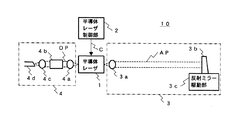
以下、図面に基づいて本発明の実施の形態を説明する。図1は、本発明の短光パルス発生装置10の構成を示している。
短光パルス発生装置10は、半導体レーザ1、半導体レーザ制御部2、帰還部3、出力部4を有している。
半導体レーザ1は、例えば分布帰還型(DFB)、分布反射型(DBR)等の半導体レーザである。
半導体レーザ1は、後述する半導体レーザ制御部2により制御され、両出射端面から光パルスを周期的に出力する。
半導体レーザ制御部2は、半導体レーザ1を駆動するための注入電流Cを出力する。半導体レーザ1の閾値電流以上の注入電流を印加している時間が、緩和振動の1周期となるようにする。
例えば、注入電流を図2の(a)のように正弦波変調する場合には、正弦波変調の変調度を大きくして、閾値電流以下まで深く変調を行う。変調度を大きくしていくと、同図(b)に示すようにキャリア密度は、注入電流Cに従って立ち上がり、その後、正弦波変調周期よりも短い周期で緩和振動する。
同図(c)に示すように光出力パワーも、同様に緩和振動する。キャリア密度の緩和振動の1周期が終わるタイミングで、注入電流がしきい値電流以下になるように、言い換えれば緩和振動の1周期が終わるタイミングで発振を止めるように制御することにより、緩和周波数の逆数で決まる時間幅の光パルスを得ることができる。光出力パワーの振動の位相は、キャリア密度の振動の位相に対してほぼπ/2遅れる。
注入電流Cは、正弦波状であってもパルス状であってもよい。なお、パルス状の注入電流Cで半導体レーザ1を駆動する場合の駆動方法は、上記した正弦波状の注入電流Cで駆動する場合と同様である。
したがって、図2の(a)のように半導体レーザ1の注入電流Cを正弦波変調すると、同図(c)のように、緩和振動周波数で決まる時間幅の光パルスが、注入電流Cの繰り返し周期で発生する。
帰還部3は、マイクロレンズ3aと反射ミラー3bと反射ミラー駆動部3cとを備える。半導体レーザ1から出射された光パルスは、コリメートされた光パルスAPに変換され空気中を伝搬する。空気中を伝搬する光パルスAPは、反射ミラー3bで同一方向かつ逆向きに反射され、マイクロレンズ3aを経由して半導体レーザ1に帰還される。反射ミラー駆動部3cは、反射ミラー3bの位置を光パルスAPの光軸に沿って動かし、半導体レーザ1からの光パルスの出射タイミングと半導体レーザ1への光パルスの帰還タイミングとを最適化する。
出力部4は、マイクロレンズ4a、アイソレータ4b、マイクロレンズ4c、出力光ファイバ4dを備え、短光パルス発生装置10としての出力光パルスOPを取り出す。
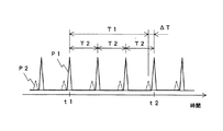
図3は、半導体レーザ1より出力される光パルスP1と、反射ミラー3bから帰還される光パルスP2との時間的な関係を表す。半導体レーザ1から出射されてから、反射ミラー3bで反射されて半導体レーザ1に帰還されるまでの時間をT1、出射された光パルスの時間間隔をT2とする。タイミングジッタを抑圧するために、T1=M・T2−ΔT(Mは自然数)が成り立つように、反射ミラー駆動部3cを用いて反射ミラー3bの位置を制御する。ΔTだけ差し引いているのは、光パルスP1の出射前に半導体レーザ1に帰還光パルスP2をフィードバックすることを意味する。
図3は、M=3の場合を表している。M=3の場合、時刻t1に出射された光パルスは、時刻t1よりも(3・T2)だけ遅い時刻t2に光パルスが出射されるより、ΔTだけ前に帰還される。
前記した特許文献1には、変調周波数1.5GHzの場合、ΔTの値は20ps〜100psである旨、記載されている。すなわち、タイミングジッタを抑圧するために要求されるΔTの値は、80psの時間幅があるため、反射ミラー3bの位置制御には±6mmの余裕がある。
例えば、半導体レーザ1への注入電流の変調周波数を1GHzとした場合、T2=1nsとなる。M=3、ΔT=100psの場合には、半導体レーザ1と反射ミラー3bとの距離は、435mmであり、非常に長くなる。このような場合には、半導体レーザ1と反射ミラー3bとの間を、折り返し光路を採用して空間的スペースを節約する方法や、引き回しが容易な光ファイバを用いる方法等がある。
図4は、半導体レーザ1と反射ミラー3bとの間の光路の一部を、偏波維持光ファイバ3eで構成した短光パルス発生装置10’の実施形態の構成を示している。偏波維持光ファイバ3eは、コアの両側にそれぞれ応力付与部を有し、入射光の偏光状態は、2つの応力付与部を貫く方向、もしくは、2つの応力付与部を貫く方向に垂直な方向の直線偏光の場合に、維持される。
なお、半導体レーザ1から出射される光パルスの偏光方向と、帰還される光パルスの偏光方向との差異が少ないほど、出力光パルスのタイミングジッタを抑圧する効果が高く、用いる光ファイバとしては偏波維持光ファイバ3eが最も適している。
偏波維持光ファイバ3eを用いる場合、帰還部3’は、さらに、半導体レーザ1からの光パルスBPを偏波維持光ファイバ3eに結合させるためのマイクロレンズ3a’と、反射ミラー3bと、偏波維持光ファイバ3eから出射された光パルスを平行ビームに変換するとともに、反射ミラー3bで同一方向かつ逆向きに反射された光パルスを偏波維持光ファイバ3eに結合させるためのマイクロレンズ3dとを備える。
なお、偏波維持光ファイバ3eの代わりに、偏波維持型でないシングルモード光ファイバを用い、半導体レーザ1と反射ミラー3bとの間に、光パルスの偏光状態を制御できる偏光コントローラを設置する構成としてもよい。
(第2の実施形態)
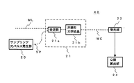
前記第1の実施形態の短光パルス発生装置10、10’をサンプリングパルス発生部20に用いた光サンプリングオシロスコープ30の実施の形態を説明する。図5は、本発明の光サンプリングオシロスコープ30の構成を示している。
光サンプリングオシロスコープ30は、サンプリングパルス発生部20、光サンプリング部21、受光部22、表示部23を有している。
サンプリング光パルス発生部20は、前記した第1の実施形態の短光パルス発生装置10、10’により構成され、サンプリング光パルスSPを発生する。サンプリング光パルスSPの繰り返し周期は、短光パルス発生装置10、10’に含まれる半導体レーザ1の変調周波数の逆数となる。被測定信号光MLの波形を正確に測定するためには、サンプリング光パルスSPの繰り返し周期を、被測定信号光MLの繰り返し周期の自然数倍からわずかな時間だけずれた周期に設定する。
なお、光サンプリングオシロスコープ30の時間分解能は、サンプリング光パルスSPのパルス幅の2乗と繰り返しジッタの2乗を足して平方根をとった値になる。
分散補償ファイバやファイバブラッググレーティング等を用いて、前記実施形態の短光パルス発生装置10、10’からの出力光パルスを圧縮(光パルスの時間幅を狭くすること)し、圧縮された光パルスを光サンプリングオシロスコープ30のサンプリング光パルスSPとしてもよい。これにより、光サンプリングオシロスコープ30の時間分解能を向上させることができる。
光サンプリング部21は、非線形光学結晶21bと、被測定信号光MLとサンプリング光パルスSPとを合波する合波器21aとを備えている。非線形光学結晶21bは、被測定信号光MLとサンプリング光パルスSPとが同時に入射され、被測定信号光MLがサンプリングされると、相互相関光MCを出力する。
たとえば、非線形光学結晶21bがKTP結晶(KTiOPO4)の場合、相互相関光MCは、サンプリングポイントにおける被測定信号光MLのパワーとサンプリング光パルスSPのピークパワーとの積に比例したパワーを有した和周波光である。被測定信号光MLの光周波数をf1、サンプリング光パルスSPの光周波数をf2とすると、相互相関光MCの光周波数は(f1+f2)である。
受光部22は、非線形光学結晶21bの後段に設置され、受光した相互相関光MCを電気信号に変換する。
表示部23は、被測定信号光MCの繰り返しに同期したトリガ信号TRを受けて、トリガ信号TRに基づいて、受光部22からの電気信号を、時間軸上に表示する。被測定信号光MCの繰り返しに同期したトリガ信号TRとは、例えば被測定信号光MLがNRZ(Non−Return−to−Zero)信号の場合、被測定信号光MLを再生して得られたクロック信号を適宜分周した信号をいい、被測定信号光MLが同じ光波形の繰り返しからなる場合、その繰り返しに同期した信号をいう。
なお、表示部23は、トリガ信号TRに応じて、受光部22からの電気のアナログ信号を電気のデジタル信号にA/D変換する機能を有する。第2の実施形態のより、被測定信号光MLの繰り返し波形もしくはアイパターンを測定できる。
(第3の実施形態)
前記第1の実施形態の短光パルス発生装置10、10’をサンプリングパルス発生部20に用いた光信号品質モニタ40の実施の形態を説明する。図6は、本発明の光信号品質モニタ40の構成を示している。なお、第3の実施形態は、第2の実施形態において用いたトリガ信号TRを用いない点、および、表示部23の代わりにQ値算出部24を用いている点で異なる。このため、第3の実施形態では、被測定信号光MLの繰り返し波形やアイパターンの測定はできないが、相互相関光MCの振幅分布の時間平均を解析することにより、被測定信号光MLのQ値を求めることができる。
Q値と信号対雑音S/N比(SNR)とは、SNR=4Q2なる関係を有する。得られたQ値からある程度ビット誤り率(BER)を推定できる。例えば、Q=6は、およそBER=10−9に相当する。このように、ネットワーク上を伝送される光信号のパターンが未知であってもビット誤り率を推定できる。このため、例えばフォトニックネットワークのように、伝送している光信号を電気信号に変換せずに光のまま中継するネットワークにおいて、実際に伝送されている光信号の品質を監視することができる。
(第2の実施形態、第3の実施形態のさらなる特徴)
モード同期レーザは、光共振器中に光変調器を配置して、光変調器の変調周波数と光共振器の共振周波数とを同期関係に調整することにより短光パルスを発生させる。このようなモード同期レーザをサンプリング光パルス発生部20に用いる場合、光変調器の変調周波数を高い周波数に設定して得られた、繰り返し周波数が変調周波数に等しくパルス幅の短い出力光パルスを間引いて、高時間分解能、低サンプリングレートを実現している。
例えば、モード同期レーザを構成する光共振器中の光変調器の変調周波数を10GHz、サンプリング光パルスSPの繰り返し周波数をたとえば10MHzに設定する。
本発明の短光パルス発生装置10、10’では、光パルス幅は、注入電流Cの変調周波数ではなく半導体レーザ1の緩和振動周波数で決まる。ゆえに、本発明の短光パルス発生装置10、10’を光サンプリングオシロスコープ30又は光信号品質モニタ40のサンプリングパルス発生部20に用いる場合、半導体レーザ1の変調周波数を、光サンプリングオシロスコープ30等のサンプリングレートのような低い周波数に設定しても短光パルスが得られる。そのため、光ゲート素子を用いた光パルスの間引きが不要となる。
なお、第2の実施形態および第3の実施形態の光サンプリング部21は、非線形光学結晶21bを用いた構成とする代わりに、サンプリング光パルスSPを受けてその波形を正確に電気変換するだけの帯域を有する受光器と、受光器からの電気信号に応じて入力光(被測定信号光ML)の透過率が変化する電界吸収型光変調器とを組み合わせたサンプリングヘッドを用いた構成としてもよい。
(First embodiment)
Hereinafter, embodiments of the present invention will be described with reference to the drawings. FIG. 1 shows the configuration of a short
The short
The
The
The semiconductor
For example, when the injection current is sinusoidally modulated as shown in FIG. 2A, the modulation degree of the sinusoidal modulation is increased and the modulation is deeply performed to the threshold current or less. When the degree of modulation is increased, the carrier density rises according to the injection current C as shown in FIG. 5B, and thereafter relaxes and oscillates at a cycle shorter than the sine wave modulation cycle.
As shown in FIG. 5C, the optical output power similarly undergoes relaxation oscillation. By controlling so that the injection current becomes equal to or less than the threshold current at the timing when one cycle of the relaxation oscillation of the carrier density ends, in other words, by controlling so that the oscillation is stopped at the timing when one cycle of the relaxation oscillation ends. An optical pulse having a time width determined by the reciprocal can be obtained. The phase of oscillation of the optical output power is delayed by approximately π / 2 with respect to the phase of oscillation of the carrier density.
The injection current C may be sinusoidal or pulsed. The driving method when the
Therefore, when the injection current C of the
The
The
FIG. 3 shows a temporal relationship between the light pulse P1 output from the
FIG. 3 shows a case where M = 3. When M = 3, the light pulse emitted at time t1 is fed back by ΔT before the light pulse is emitted at time t2 later by (3 · T2) than time t1.
For example, when the modulation frequency of the injection current to the
FIG. 4 shows a configuration of an embodiment of a short
The smaller the difference between the polarization direction of the light pulse emitted from the
When the polarization maintaining optical fiber 3e is used, the
In addition, instead of the polarization maintaining optical fiber 3e, a non-polarization maintaining single mode optical fiber is used, and a polarization controller capable of controlling the polarization state of the optical pulse is installed between the
(Second Embodiment)
An embodiment of an
The
The sampling
The time resolution of the
Using a dispersion compensating fiber, a fiber Bragg grating, or the like, the output light pulse from the short
The
For example, when the nonlinear optical crystal 21b is a KTP crystal (KTiOPO 4 ), the cross-correlation light MC has a power proportional to the product of the power of the signal light ML to be measured at the sampling point and the peak power of the sampling light pulse SP. It is sum frequency light. When the optical frequency of the signal light to be measured ML is f1 and the optical frequency of the sampling light pulse SP is f2, the optical frequency of the cross-correlation light MC is (f1 + f2).
The
The display unit 23 receives the trigger signal TR synchronized with the repetition of the signal light to be measured MC, and displays the electrical signal from the
The display unit 23 has a function of A / D converting an electrical analog signal from the
(Third embodiment)
An embodiment of an optical signal quality monitor 40 using the short
The Q value and the signal-to-noise S / N ratio (SNR) have a relationship of SNR = 4Q 2 . The bit error rate (BER) can be estimated to some extent from the obtained Q value. For example, Q = 6 corresponds to approximately BER = 10 −9 . Thus, even if the pattern of the optical signal transmitted over the network is unknown, the bit error rate can be estimated. For this reason, the quality of the optical signal that is actually transmitted can be monitored in a network that relays the transmitted optical signal as it is without converting it into an electrical signal, such as a photonic network.
(Further features of the second embodiment and the third embodiment)
In a mode-locked laser, an optical modulator is disposed in an optical resonator, and a short optical pulse is generated by adjusting the modulation frequency of the optical modulator and the resonant frequency of the optical resonator in a synchronous relationship. When such a mode-locked laser is used for the sampling
For example, the modulation frequency of the optical modulator in the optical resonator constituting the mode-locked laser is set to 10 GHz, and the repetition frequency of the sampling light pulse SP is set to 10 MHz, for example.
In the short
Note that the
1……半導体レーザ、2……半導体レーザ制御部、3……帰還部、3b……反射ミラー、3c……反射ミラー駆動部、3a、3a’、3d……マイクロレンズ、3e……偏波維持光ファイバ、4……出力部、4b……アイソレータ、4a、4c……マイクロレンズ、4d……出力光ファイバ、10、10’……短光パルス発生装置、20……サンプリング光パルス発生部、21……光サンプリング部、21a……合波部、21b……非線形光学結晶、22……受光部、23……表示部、24……Q値算出部、30……光サンプリングオシロスコープ、40……光信号品質モニタ。
DESCRIPTION OF
Claims (3)
前記半導体レーザに対して、変調された注入電流を印加する半導体レーザ制御部と、
前記半導体レーザの一方の端面から前記注入電流の繰り返し周期に等しい周期で出射された各光パルスを、対応する新たな光パルスの出射前に、前記半導体レーザに帰還させる帰還部と、
出力光パルスを取り出す出力部とを備えた短光パルス発生装置において、
前記出力部(4)は、調整不要に固定され、前記半導体レーザの前記一方の端面とは異なる他方の端面から出射された光パルスを、前記出力光パルスとして取り出すことを特徴とする短光パルス発生装置。
A semiconductor laser;
A semiconductor laser controller for applying a modulated injection current to the semiconductor laser;
A feedback unit that feeds back each optical pulse emitted from one end face of the semiconductor laser at a period equal to the repetition period of the injection current to the semiconductor laser before emission of the corresponding new optical pulse;
In a short light pulse generator having an output unit for extracting an output light pulse,
The output unit (4) is fixed without adjustment, and takes out an optical pulse emitted from the other end face different from the one end face of the semiconductor laser as the output optical pulse. Generator.
前記被測定信号光を前記サンプリング光パルスでサンプリングし、サンプリングにより得られた相互相関光(MC)を出力する光サンプリング部(21)と、
前記相互相関光を電気信号に変換する受光部(22)と、
前記被測定信号光の繰り返しに同期したトリガ信号(TR)に基づいて、前記電気信号を表示する表示部(23)とを備えた光サンプリングオシロスコープにおいて、
前記サンプリング光パルス発生部(20)は、請求項1に記載の短光パルス発生装置(10、10’)であることを特徴とする光サンプリングオシロスコープ。
A sampling light pulse generator for generating a sampling light pulse (SP) having a period different by a predetermined offset time with respect to a natural number multiple of the repetition period of the signal light to be measured (ML);
An optical sampling unit (21) for sampling the signal light under measurement with the sampling light pulse and outputting a cross-correlation light (MC) obtained by the sampling;
A light receiving unit (22) for converting the cross-correlation light into an electrical signal;
In an optical sampling oscilloscope comprising a display unit (23) for displaying the electrical signal based on a trigger signal (TR) synchronized with repetition of the signal light under measurement,
The optical sampling oscilloscope, wherein the sampling optical pulse generator (20) is the short optical pulse generator (10, 10 ') according to claim 1.
前記被測定信号光を前記サンプリング光パルスでサンプリングし、サンプリングにより得られた相互相関光(MC)を出力する光サンプリング部(21)と、
前記相互相関光を電気信号に変換する受光部(22)と、
前記電気信号に基づいて、前記被測定信号光のQ値を算出するQ値算出部(24)とを備えた光信号品質モニタにおいて、
前記サンプリング光パルス発生部(20)は、請求項1に記載の短光パルス発生装置(10、10’)であることを特徴とする光信号品質モニタ。 A sampling light pulse generator for generating a sampling light pulse (SP) having a period different by a predetermined offset time with respect to a natural number multiple of the repetition period of the signal light to be measured (ML);
An optical sampling unit (21) for sampling the signal light under measurement with the sampling light pulse and outputting a cross-correlation light (MC) obtained by the sampling;
A light receiving unit (22) for converting the cross-correlation light into an electrical signal;
In an optical signal quality monitor comprising a Q value calculation unit (24) for calculating a Q value of the signal light under measurement based on the electrical signal,
The optical signal quality monitor according to claim 1, wherein the sampling optical pulse generator (20) is the short optical pulse generator (10, 10 ') according to claim 1.
Priority Applications (1)
| Application Number | Priority Date | Filing Date | Title |
|---|---|---|---|
| JP2007176223A JP2009016546A (en) | 2007-07-04 | 2007-07-04 | Short light pulse generating device, light sampling oscilloscope using the same, and light signal quality monitor |
Applications Claiming Priority (1)
| Application Number | Priority Date | Filing Date | Title |
|---|---|---|---|
| JP2007176223A JP2009016546A (en) | 2007-07-04 | 2007-07-04 | Short light pulse generating device, light sampling oscilloscope using the same, and light signal quality monitor |
Publications (1)
| Publication Number | Publication Date |
|---|---|
| JP2009016546A true JP2009016546A (en) | 2009-01-22 |
Family
ID=40357103
Family Applications (1)
| Application Number | Title | Priority Date | Filing Date |
|---|---|---|---|
| JP2007176223A Pending JP2009016546A (en) | 2007-07-04 | 2007-07-04 | Short light pulse generating device, light sampling oscilloscope using the same, and light signal quality monitor |
Country Status (1)
| Country | Link |
|---|---|
| JP (1) | JP2009016546A (en) |
Citations (9)
| Publication number | Priority date | Publication date | Assignee | Title |
|---|---|---|---|---|
| JPH0661586A (en) * | 1992-08-07 | 1994-03-04 | Nippon Telegr & Teleph Corp <Ntt> | Light control pulse laser |
| JPH07159247A (en) * | 1993-12-06 | 1995-06-23 | Anritsu Corp | Light waveform measuring apparatus |
| JP2597845B2 (en) * | 1987-06-09 | 1997-04-09 | 浜松ホトニクス株式会社 | High repetition pulse laser equipment |
| JPH11223575A (en) * | 1997-12-01 | 1999-08-17 | Nippon Telegr & Teleph Corp <Ntt> | Quality monitor for light signal |
| JPH11243246A (en) * | 1998-02-24 | 1999-09-07 | Nippon Telegr & Teleph Corp <Ntt> | External resonator semiconductor laser |
| JP2002164614A (en) * | 2000-11-28 | 2002-06-07 | Nec Corp | External resonator type mode synchronization semiconductor laser system |
| JP2003090766A (en) * | 2001-07-13 | 2003-03-28 | Nippon Telegr & Teleph Corp <Ntt> | Method and apparatus for monitoring optical signal quality deterioration factor |
| WO2005006508A1 (en) * | 2003-07-11 | 2005-01-20 | Kochi University Of Technology | Short light pluse generator |
| JP2005197511A (en) * | 2004-01-08 | 2005-07-21 | Hamamatsu Photonics Kk | Optical pulse generator |
-
2007
- 2007-07-04 JP JP2007176223A patent/JP2009016546A/en active Pending
Patent Citations (9)
| Publication number | Priority date | Publication date | Assignee | Title |
|---|---|---|---|---|
| JP2597845B2 (en) * | 1987-06-09 | 1997-04-09 | 浜松ホトニクス株式会社 | High repetition pulse laser equipment |
| JPH0661586A (en) * | 1992-08-07 | 1994-03-04 | Nippon Telegr & Teleph Corp <Ntt> | Light control pulse laser |
| JPH07159247A (en) * | 1993-12-06 | 1995-06-23 | Anritsu Corp | Light waveform measuring apparatus |
| JPH11223575A (en) * | 1997-12-01 | 1999-08-17 | Nippon Telegr & Teleph Corp <Ntt> | Quality monitor for light signal |
| JPH11243246A (en) * | 1998-02-24 | 1999-09-07 | Nippon Telegr & Teleph Corp <Ntt> | External resonator semiconductor laser |
| JP2002164614A (en) * | 2000-11-28 | 2002-06-07 | Nec Corp | External resonator type mode synchronization semiconductor laser system |
| JP2003090766A (en) * | 2001-07-13 | 2003-03-28 | Nippon Telegr & Teleph Corp <Ntt> | Method and apparatus for monitoring optical signal quality deterioration factor |
| WO2005006508A1 (en) * | 2003-07-11 | 2005-01-20 | Kochi University Of Technology | Short light pluse generator |
| JP2005197511A (en) * | 2004-01-08 | 2005-07-21 | Hamamatsu Photonics Kk | Optical pulse generator |
Similar Documents
| Publication | Publication Date | Title |
|---|---|---|
| US6816515B1 (en) | Wavelength-swept laser and method for its operation | |
| JP3688841B2 (en) | Laser pulse comparison method, high-speed laser scanning method, high-speed scanning laser device, short pulse laser device, distance measuring device, electro-optic sampling oscilloscope, short pulse laser stability control method, and calibration time scale generator | |
| JP2004503944A (en) | Method and apparatus for generating frequency modulated pulses | |
| US8625191B2 (en) | Wavelength-tunable light source apparatus | |
| US6957019B2 (en) | Stabilized optical pulse generator | |
| JP2008251723A (en) | Pulse laser light source | |
| US9197326B2 (en) | Optical wavelength comb generator device | |
| US11409032B2 (en) | Fiber amplifier system resistance to nonlinear spectral broadening and decoherence | |
| Zhou et al. | Linear frequency-modulated waveform generation based on a tunable optoelectronic oscillator | |
| US20210159661A1 (en) | Laser Device for Generating an Optical Frequency Comb | |
| JP2009016546A (en) | Short light pulse generating device, light sampling oscilloscope using the same, and light signal quality monitor | |
| JP3573334B2 (en) | Light generation method and light source | |
| JP3849019B2 (en) | Method and apparatus for reducing timing jitter of optical pulse | |
| JP5342096B2 (en) | Short light pulse generator | |
| Chan et al. | Electrically wavelength-tunable pulses generated by synchronous two-way injection seeding | |
| Vu et al. | Detailed comparison of injection-seeded and self-seeded performance of a 1060-nm gain-switched Fabry–Pérot laser diode | |
| JP4408246B2 (en) | Mode-locked semiconductor laser | |
| RU2639552C1 (en) | Method for forming synchronous sequences of ultrashort laser pulses and femtosecond laser complex | |
| Maher et al. | Cavity Length Independent Continuous Repetition Rate Tuning of a Self-Seeded Gain-Switched Fabry–Pérot Laser | |
| Zhou et al. | Coherent combining of two pulsed fibre lasers in phase modulated mutually coupled fibre laser array | |
| JP2009162838A (en) | Device and method for generating optical pulse | |
| Anandarajah et al. | Continuous Repetition Rate Tuning with Timing Window Independent Self-Seeding of a Gain-Switched Fabry-Perot Laser | |
| Delfyett et al. | Stabilized Mode-locked Diode Lasers & Applications | |
| Filion et al. | Tunable mode-locked fiber laser with a highly dispersive cavity | |
| Lu et al. | External modulation technique for the generation of strict linearly chirped continuous waves |
Legal Events
| Date | Code | Title | Description |
|---|---|---|---|
| A977 | Report on retrieval |
Effective date: 20110125 Free format text: JAPANESE INTERMEDIATE CODE: A971007 |
|
| A131 | Notification of reasons for refusal |
Effective date: 20111108 Free format text: JAPANESE INTERMEDIATE CODE: A131 |
|
| A521 | Written amendment |
Free format text: JAPANESE INTERMEDIATE CODE: A523 Effective date: 20111228 |
|
| A131 | Notification of reasons for refusal |
Free format text: JAPANESE INTERMEDIATE CODE: A131 Effective date: 20120306 |
|
| A02 | Decision of refusal |
Effective date: 20120703 Free format text: JAPANESE INTERMEDIATE CODE: A02 |