JP2009010248A - Surface emitting laser and method of manufacturing the same - Google Patents
Surface emitting laser and method of manufacturing the same Download PDFInfo
- Publication number
- JP2009010248A JP2009010248A JP2007171579A JP2007171579A JP2009010248A JP 2009010248 A JP2009010248 A JP 2009010248A JP 2007171579 A JP2007171579 A JP 2007171579A JP 2007171579 A JP2007171579 A JP 2007171579A JP 2009010248 A JP2009010248 A JP 2009010248A
- Authority
- JP
- Japan
- Prior art keywords
- emitting laser
- surface emitting
- substrate
- current
- region
- Prior art date
- Legal status (The legal status is an assumption and is not a legal conclusion. Google has not performed a legal analysis and makes no representation as to the accuracy of the status listed.)
- Pending
Links
Images


Classifications
-
- H—ELECTRICITY
- H01—ELECTRIC ELEMENTS
- H01S—DEVICES USING THE PROCESS OF LIGHT AMPLIFICATION BY STIMULATED EMISSION OF RADIATION [LASER] TO AMPLIFY OR GENERATE LIGHT; DEVICES USING STIMULATED EMISSION OF ELECTROMAGNETIC RADIATION IN WAVE RANGES OTHER THAN OPTICAL
- H01S5/00—Semiconductor lasers
- H01S5/10—Construction or shape of the optical resonator, e.g. extended or external cavity, coupled cavities, bent-guide, varying width, thickness or composition of the active region
- H01S5/18—Surface-emitting [SE] lasers, e.g. having both horizontal and vertical cavities
- H01S5/183—Surface-emitting [SE] lasers, e.g. having both horizontal and vertical cavities having only vertical cavities, e.g. vertical cavity surface-emitting lasers [VCSEL]
- H01S5/18386—Details of the emission surface for influencing the near- or far-field, e.g. a grating on the surface
- H01S5/18394—Apertures, e.g. defined by the shape of the upper electrode
-
- H—ELECTRICITY
- H01—ELECTRIC ELEMENTS
- H01S—DEVICES USING THE PROCESS OF LIGHT AMPLIFICATION BY STIMULATED EMISSION OF RADIATION [LASER] TO AMPLIFY OR GENERATE LIGHT; DEVICES USING STIMULATED EMISSION OF ELECTROMAGNETIC RADIATION IN WAVE RANGES OTHER THAN OPTICAL
- H01S5/00—Semiconductor lasers
- H01S5/10—Construction or shape of the optical resonator, e.g. extended or external cavity, coupled cavities, bent-guide, varying width, thickness or composition of the active region
- H01S5/18—Surface-emitting [SE] lasers, e.g. having both horizontal and vertical cavities
- H01S5/183—Surface-emitting [SE] lasers, e.g. having both horizontal and vertical cavities having only vertical cavities, e.g. vertical cavity surface-emitting lasers [VCSEL]
- H01S5/18305—Surface-emitting [SE] lasers, e.g. having both horizontal and vertical cavities having only vertical cavities, e.g. vertical cavity surface-emitting lasers [VCSEL] with emission through the substrate, i.e. bottom emission
-
- H—ELECTRICITY
- H01—ELECTRIC ELEMENTS
- H01S—DEVICES USING THE PROCESS OF LIGHT AMPLIFICATION BY STIMULATED EMISSION OF RADIATION [LASER] TO AMPLIFY OR GENERATE LIGHT; DEVICES USING STIMULATED EMISSION OF ELECTROMAGNETIC RADIATION IN WAVE RANGES OTHER THAN OPTICAL
- H01S2301/00—Functional characteristics
- H01S2301/16—Semiconductor lasers with special structural design to influence the modes, e.g. specific multimode
- H01S2301/166—Single transverse or lateral mode
-
- H—ELECTRICITY
- H01—ELECTRIC ELEMENTS
- H01S—DEVICES USING THE PROCESS OF LIGHT AMPLIFICATION BY STIMULATED EMISSION OF RADIATION [LASER] TO AMPLIFY OR GENERATE LIGHT; DEVICES USING STIMULATED EMISSION OF ELECTROMAGNETIC RADIATION IN WAVE RANGES OTHER THAN OPTICAL
- H01S5/00—Semiconductor lasers
- H01S5/02—Structural details or components not essential to laser action
- H01S5/0206—Substrates, e.g. growth, shape, material, removal or bonding
- H01S5/0215—Bonding to the substrate
- H01S5/0216—Bonding to the substrate using an intermediate compound, e.g. a glue or solder
-
- H—ELECTRICITY
- H01—ELECTRIC ELEMENTS
- H01S—DEVICES USING THE PROCESS OF LIGHT AMPLIFICATION BY STIMULATED EMISSION OF RADIATION [LASER] TO AMPLIFY OR GENERATE LIGHT; DEVICES USING STIMULATED EMISSION OF ELECTROMAGNETIC RADIATION IN WAVE RANGES OTHER THAN OPTICAL
- H01S5/00—Semiconductor lasers
- H01S5/02—Structural details or components not essential to laser action
- H01S5/0206—Substrates, e.g. growth, shape, material, removal or bonding
- H01S5/0217—Removal of the substrate
-
- H—ELECTRICITY
- H01—ELECTRIC ELEMENTS
- H01S—DEVICES USING THE PROCESS OF LIGHT AMPLIFICATION BY STIMULATED EMISSION OF RADIATION [LASER] TO AMPLIFY OR GENERATE LIGHT; DEVICES USING STIMULATED EMISSION OF ELECTROMAGNETIC RADIATION IN WAVE RANGES OTHER THAN OPTICAL
- H01S5/00—Semiconductor lasers
- H01S5/10—Construction or shape of the optical resonator, e.g. extended or external cavity, coupled cavities, bent-guide, varying width, thickness or composition of the active region
- H01S5/18—Surface-emitting [SE] lasers, e.g. having both horizontal and vertical cavities
- H01S5/183—Surface-emitting [SE] lasers, e.g. having both horizontal and vertical cavities having only vertical cavities, e.g. vertical cavity surface-emitting lasers [VCSEL]
- H01S5/18308—Surface-emitting [SE] lasers, e.g. having both horizontal and vertical cavities having only vertical cavities, e.g. vertical cavity surface-emitting lasers [VCSEL] having a special structure for lateral current or light confinement
- H01S5/18311—Surface-emitting [SE] lasers, e.g. having both horizontal and vertical cavities having only vertical cavities, e.g. vertical cavity surface-emitting lasers [VCSEL] having a special structure for lateral current or light confinement using selective oxidation
Abstract
Description
本発明は、面発光レーザおよびその製造方法に関し、特に基本横モードによる更なる高出力と量子効率の向上を目指す面発光レーザおよびその製造方法に関するものである。 The present invention relates to a surface emitting laser and a method for manufacturing the same, and more particularly to a surface emitting laser aiming at further high output and quantum efficiency improvement by a fundamental transverse mode and a method for manufacturing the same.
従来の垂直共振器型面発光レーザ(Vertical Cavity Surface Emitting Laser、以下VCSELと略す)では、基本横モードのレーザ発振を得るため、発光領域の径を5μm程度まで狭める構成が採られていた。
そのため、活性層領域の体積が小さくなり、光出力の低下を来していた。
このようなことから、特許文献1では、基本横モード発振に影響を与えることなく、高次横モード発振を抑制するようにした面発光半導体レーザが提案されている。
この面発光半導体レーザは、図5に示すように、半導体基板101上に、下部n型DBR層103、活性領域104、上部p型DBR層106が設けられている。
上部p型DBR層106の上にあって、レーザ光の出射領域となる開口部127を有する上部p型電極108が形成されており、更に、酸化領域として形成された電流狭窄部124を備えた構成が採られている。
この面発光型半導体レーザは、以上の構成において、上部p型電極108に対応する共振器の反射率に基づいて、レーザ光の高次横モードと基本横モードとにおける共振器の光学損失の差が大きくなるように、電流狭窄部の開口径と電極の開口部径とが決定される。
すなわち、このようにして、活性層近傍に設けられ、電流の経路を制限するために挿入される電流狭窄部の開口径と、レーザ光を出射するために形成された電極の開口部径とが決定され、基本横モードで高い光出力が達成される。
For this reason, the volume of the active layer region is reduced, resulting in a decrease in light output.
For this reason,
As shown in FIG. 5, the surface emitting semiconductor laser includes a lower n-
An upper p-
In this surface emitting semiconductor laser, the difference in the optical loss of the resonator between the high-order transverse mode and the fundamental transverse mode of the laser light is based on the reflectance of the resonator corresponding to the upper p-
That is, the opening diameter of the current confinement portion provided in the vicinity of the active layer and inserted in order to limit the current path in this way, and the opening diameter of the electrode formed to emit laser light are And high light output is achieved in the fundamental transverse mode.
メサ構造の発光素子において、活性層近傍に設けられる電流狭窄部は、メサ構造の加工面を流れる漏洩電流を低減する上で、非常に効果があり、高効率のメサ型VCSELにおいて極めて重要な構成となっている。
一方、レーザ発振は、共振器の反射特性の他に、活性層における発光再結合(利得)分布にも依存している。
特に、酸化領域によって活性層に注入する電流の経路を制限する(電流狭窄を行う)開口部を有する電流狭窄部の構造では、電流は開口部に制限されるが、開口部の周辺部に集中するため、必然的に利得が大きくなり、高次横モードが励起される。したがって、特許文献1のように、共振器の反射損失を制御して、基本横モード発振を実現する構成では、上記したように高次横モードの利得は増大してしまうので、共振器の反射損失を増大させて、高次横モードを抑圧させることとなる。
そのため、このように従来例においては、注入電力を光出力に変換される際の効率(量子効率)の点で、課題を有している。
また、電流狭窄領域の酸化領域の屈折率と、酸化されていない領域の屈折率の差が大きいため、導波光が強く閉じ込められる屈折率導波型となり、高次横モードが立ち易い導波路構造である点においても、課題を有している。
In the mesa structure light emitting device, the current confinement portion provided in the vicinity of the active layer is very effective in reducing the leakage current flowing through the processing surface of the mesa structure, and is an extremely important configuration in a high efficiency mesa type VCSEL. It has become.
On the other hand, laser oscillation depends not only on the reflection characteristics of the resonator but also on the light emission recombination (gain) distribution in the active layer.
In particular, in the structure of the current confinement portion having an opening that restricts the path of current injected into the active layer by the oxidized region (performs current confinement), the current is restricted to the opening, but is concentrated on the periphery of the opening. Therefore, the gain is inevitably increased, and a high-order transverse mode is excited. Therefore, in the configuration in which the fundamental transverse mode oscillation is realized by controlling the reflection loss of the resonator as in
For this reason, the conventional example has a problem in terms of efficiency (quantum efficiency) when the injection power is converted into the optical output.
In addition, because the difference between the refractive index of the oxidized region in the current confinement region and the refractive index of the non-oxidized region is large, the waveguide structure is a refractive index waveguide type in which guided light is strongly confined, and a high-order transverse mode is easily generated. Even in this respect, there is a problem.
本発明は、上記課題に鑑み、高次横モード発振を抑制しながら基本横モードを維持することができ、一層の高出力が可能となる面発光レーザおよびその製造方法の提供を目的とする。 The present invention has been made in view of the above problems, and an object of the present invention is to provide a surface emitting laser capable of maintaining a fundamental transverse mode while suppressing higher-order transverse mode oscillation and capable of further high output, and a method for manufacturing the same.
本発明は、以下のように構成した面発光レーザおよびその製造方法を提供するものである。
本発明の面発光レーザは、活性層に電流を注入する経路となる開口部を備え、該開口部の周辺に設けられている電流狭窄領域を有する面発光レーザであって、
前記活性層を挟んで光出射側と反対側に設けられた電流注入領域を備え、
前記電流注入領域における電流注入経路の径が、前記開口部の径よりも小さい径によって構成されていることを特徴とする。
また、本発明の面発光レーザは、前記電流狭窄領域は、前記活性層における光強度分布の最大強度の50%以下であることを特徴とする。
また、本発明の面発光レーザは、前記電流注入領域における電流注入経路の径をDiとし、前記開口部の径をDoとするとき、つぎの関係式(1)を満たすことを特徴とする。
Di<Do−4(μm)………(1)
また、本発明の面発光レーザは、前記電流注入領域が、基板に形成された配線パターンに接合させて構成されていることを特徴とする。
また、本発明の面発光レーザは、前記配線パターンが形成された基板が、シリコンによる基板、アルミナによる基板、絶縁膜が形成されたCuWによる基板、のうちのいずれかの基板であることを特徴とする。
また、本発明の面発光レーザは、前記配線パターンが形成された基板がシリコン基板であり、該基板に面発光レーザを駆動する駆動回路が形成されていることを特徴とする。
また、本発明の面発光レーザアレイは、上記したいずれかに記載の面発光レーザが、一次元または、二次元に配列されていることを特徴とする。
また、本発明の面発光レーザの製造方法は、活性層に電流を注入する経路となる開口部を備えた電流狭窄領域を有する面発光レーザの製造方法であって、
基板上に、前記電流狭窄領域を形成するための層を含むメサ構造の面発光レーザパターンを形成する工程と、
前記電流狭窄領域を形成するための層に、活性層に注入する電流の経路となる開口部を備え、該開口部の周辺を絶縁化して電流狭窄領域を形成する工程と、
前記メサ構造の頂部中央に、電流注入経路の径が前記電流狭窄領域の開口部の径よりも小さい径を備えた電流注入領域を、前記活性層を挟んで光出射側と反対側に形成する工程と、を有することを特徴とする。
また、本発明の面発光レーザの製造方法は、前記電流注入領域を形成した後、該電流注入領域を形成した面を配線パターンが形成された別基板に対面させて接合する工程を、更に有することを特徴とする。
また、本発明の面発光レーザの製造方法は、前記電流注入領域を形成した面を配線パターンが形成された別基板に対面させて接合した後、面発光レーザパターンを形成する工程で用いた前記基板を除去する工程を、更に有することを特徴とする。
また、本発明の面発光レーザの製造方法は、前記メサ構造の面発光レーザパターンを形成する工程で用いる基板がGaAs基板であり、
前記電流注入領域を形成した面を配線パターンが形成された別基板に対面させて接合する工程で用いる基板がシリコン基板であることを特徴とする。
The present invention provides a surface emitting laser configured as follows and a method for manufacturing the same.
A surface-emitting laser according to the present invention is a surface-emitting laser that includes an opening serving as a path for injecting a current into an active layer and includes a current confinement region provided around the opening.
A current injection region provided on the side opposite to the light emitting side across the active layer,
The diameter of the current injection path in the current injection region is configured to be smaller than the diameter of the opening.
In the surface emitting laser of the present invention, the current confinement region is 50% or less of the maximum intensity of the light intensity distribution in the active layer.
The surface emitting laser of the present invention is characterized in that the following relational expression (1) is satisfied, where Di is the diameter of the current injection path in the current injection region and Do is the diameter of the opening.
Di <Do-4 (μm) (1)
The surface emitting laser according to the present invention is characterized in that the current injection region is formed by bonding to a wiring pattern formed on a substrate.
In the surface emitting laser of the present invention, the substrate on which the wiring pattern is formed is any one of a substrate made of silicon, a substrate made of alumina, and a substrate made of CuW on which an insulating film is formed. And
In the surface emitting laser according to the present invention, the substrate on which the wiring pattern is formed is a silicon substrate, and a driving circuit for driving the surface emitting laser is formed on the substrate.
Moreover, the surface emitting laser array of the present invention is characterized in that any of the surface emitting lasers described above is arranged one-dimensionally or two-dimensionally.
A method for manufacturing a surface emitting laser according to the present invention is a method for manufacturing a surface emitting laser having a current confinement region having an opening serving as a path for injecting a current into an active layer,
Forming a surface emitting laser pattern having a mesa structure including a layer for forming the current confinement region on the substrate;
Forming a current confinement region in the layer for forming the current confinement region, comprising an opening serving as a path for a current to be injected into the active layer, and insulating the periphery of the opening;
At the center of the top of the mesa structure, a current injection region having a diameter of a current injection path smaller than the diameter of the opening of the current confinement region is formed on the side opposite to the light emitting side with the active layer interposed therebetween. And a process.
The method of manufacturing a surface emitting laser according to the present invention further includes a step of forming the current injection region and then bonding the surface on which the current injection region is formed to another substrate on which a wiring pattern is formed. It is characterized by that.
In addition, the surface emitting laser manufacturing method of the present invention is used in the step of forming the surface emitting laser pattern after joining the surface on which the current injection region is formed facing another substrate on which the wiring pattern is formed. The method further includes a step of removing the substrate.
Further, in the method for manufacturing a surface emitting laser according to the present invention, the substrate used in the step of forming the surface emitting laser pattern having the mesa structure is a GaAs substrate,
The substrate used in the step of joining the surface on which the current injection region is formed facing another substrate on which a wiring pattern is formed is a silicon substrate.
本発明によれば、高次横モード発振を抑制しながら基本横モードを維持することができ、一層の高出力が可能となる。 According to the present invention, the fundamental transverse mode can be maintained while suppressing higher-order transverse mode oscillation, and higher output can be achieved.
つぎに、本発明の実施の形態における面発光レーザについて説明する。
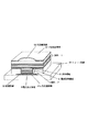
図1に、本実施形態における面発光レーザの構成例を説明する概略斜視図を示す。
図1において、5は活性領域、6は電流狭窄領域、8は電流注入領域、41はp型金属電極(下部電極)、51はシリコン基板、52は金属配線、61はn型金属電極(上部電極)、62は光放射用窓である。
本実施形態における面発光レーザは、活性領域(活性層)5を挟み、DBR−1(上部多層膜反射鏡)とDBR−2(下部多層膜反射鏡)とによって共振器が構成されている。
また、この共振器の上下に、レーザ光を出射する光放射用窓62が設けられたn型金属電極(上部電極)61と、この光放射用窓62による光出射側と反対側に設けられた電流注入領域が形成されたp型金属電極(下部電極)41を備えている。
また、活性層に隣接して設けられ、電流流路の周縁部を絶縁化して形成された開口部を備えた電流狭窄部(電流狭窄領域)6を備えている。
その際、p型金属電極(下部電極)41の前記電流注入領域における電流注入経路の径が、前記電流狭窄部6における開口部の径よりも小さくなるように構成されている。
また、本実施の形態においては、前記光出射側と反対側に設けられた電流注入領域を形成する下部電極が、配線パターンが形成された基板、または面発光レーザの駆動回路が形成された基板の配線に接合させて構成することができる。
前記配線パターンが形成された基板は、シリコン基板、アルミナによる高熱伝導絶縁基板、絶縁膜が形成されたCuWによる高熱伝導基板のいずれかによって構成することができる。
また、本実施の形態においては、上記した面発光レーザを、一次元または、二次元に配列して面発光レーザアレイを構成することができる。
Next, the surface emitting laser according to the embodiment of the present invention will be described.
FIG. 1 is a schematic perspective view illustrating a configuration example of the surface emitting laser according to the present embodiment.
In FIG. 1, 5 is an active region, 6 is a current confinement region, 8 is a current injection region, 41 is a p-type metal electrode (lower electrode), 51 is a silicon substrate, 52 is a metal wiring, and 61 is an n-type metal electrode (upper portion). Electrodes) and 62 are light emission windows.
In the surface emitting laser according to this embodiment, an active region (active layer) 5 is sandwiched, and DBR-1 (upper multilayer reflector) and DBR-2 (lower multilayer reflector) constitute a resonator.
Further, an n-type metal electrode (upper electrode) 61 provided with a light emission window 62 for emitting laser light is provided above and below the resonator, and provided on the opposite side to the light emission side of the light emission window 62. A p-type metal electrode (lower electrode) 41 in which a current injection region is formed is provided.
In addition, a current confinement portion (current confinement region) 6 is provided that is provided adjacent to the active layer and includes an opening formed by insulating the peripheral portion of the current flow path.
At this time, the diameter of the current injection path in the current injection region of the p-type metal electrode (lower electrode) 41 is configured to be smaller than the diameter of the opening in the
In the present embodiment, the lower electrode forming the current injection region provided on the side opposite to the light emitting side is a substrate on which a wiring pattern is formed, or a substrate on which a surface emitting laser driving circuit is formed. It can be configured to be joined to the wiring.
The substrate on which the wiring pattern is formed can be constituted by any of a silicon substrate, a high thermal conductive insulating substrate made of alumina, and a high thermal conductive substrate made of CuW on which an insulating film is formed.
In the present embodiment, the surface emitting laser array can be configured by arranging the surface emitting lasers described above one-dimensionally or two-dimensionally.
本実施形態における上記構成によれば、p型金属電極(下部電極)41の前記電流注入領域における電流注入経路の径が、前記電流狭窄部6における開口部の径よりも小さ径で構成することにより、電流を電流狭窄部の開口部の中心部に集中させることができる。
そのため、電流が電流狭窄部の開口部の周辺に集中することによる高次横モードの利得の増大を回避することができ、基本横モードによる高出力と量子効率の向上の実現が可能となる。
同時に、導波光の大部分が、屈折率が大きく変化する絶縁化領域から離れることによって、導波路の光閉じ込めが弱くなり、導波路特性として高次横モード発振を抑制することが可能となる。
また、本実施形態における上記構成によれば、下部電極を配線パターンが形成された基板、あるいは面発光レーザの駆動回路が形成された基板に直接接合することが可能となる。
これにより、駆動回路を含む発光装置の組み上げにおいて、実装工程におけるワイヤーボンディング数を削減でき、装置の小型化を図ることができる。
また、本実施形態における上記構成によれば、面発光デバイスを接合する基板を、熱伝導率の高い基板で構成することにより、高い光出力が得られる。
また、アレイ形態では、隣接素子の相互干渉を低減することができる。
このように、本実施形態に係る発明は、活性層に電流を注入する経路となる開口部を備え、該開口部の周辺に設けられている電流狭窄領域を有する面発光レーザであるが、必ずしもレーザに限らず、発光素子であれば、LEDであってもよい。
但し、前記活性層を挟んで光出射側と反対側に設けられた電流注入領域を備え、前記電流注入領域における電流注入経路の径が、前記開口部の径よりも小さい径によって構成されていることが特徴である点は同じである。
また、前記電流狭窄領域は、前記活性層における光強度分布の最大強度の50%以下となるようにするのがよい。より好ましくは、30%以下であり、下限は特に限定されないが、例えば、5%以上である。
According to the above configuration in the present embodiment, the diameter of the current injection path in the current injection region of the p-type metal electrode (lower electrode) 41 is configured to be smaller than the diameter of the opening in the
Therefore, it is possible to avoid an increase in the gain of the high-order transverse mode due to the current being concentrated around the opening of the current confinement part, and it is possible to realize a high output and an improvement in quantum efficiency by the basic transverse mode.
At the same time, since most of the guided light is separated from the insulating region where the refractive index changes greatly, the optical confinement of the waveguide becomes weak, and high-order transverse mode oscillation can be suppressed as waveguide characteristics.
Further, according to the above configuration in the present embodiment, the lower electrode can be directly bonded to the substrate on which the wiring pattern is formed or the substrate on which the surface emitting laser drive circuit is formed.
Thereby, in the assembly of the light emitting device including the drive circuit, the number of wire bondings in the mounting process can be reduced, and the device can be miniaturized.
Moreover, according to the said structure in this embodiment, a high light output is obtained by comprising the board | substrate which joins a surface emitting device with a board | substrate with high thermal conductivity.
In the array form, mutual interference between adjacent elements can be reduced.
As described above, the invention according to the present embodiment is a surface emitting laser that includes an opening serving as a path for injecting a current into an active layer and has a current confinement region provided around the opening. Not only a laser but also a LED may be used as long as it is a light emitting element.
However, a current injection region provided on the side opposite to the light emitting side across the active layer is provided, and the diameter of the current injection path in the current injection region is configured to be smaller than the diameter of the opening. This is the same point.
The current confinement region may be 50% or less of the maximum intensity of the light intensity distribution in the active layer. More preferably, it is 30% or less, and the lower limit is not particularly limited, but is, for example, 5% or more.
つぎに、本発明の実施の形態における面発光レーザの製造方法について説明する。
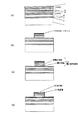
図2及び図3に、本実施形態における面発光レーザの製造方法を説明する図を示す。
図2(a)〜(d)は本実施形態における面発光レーザの製造方法を説明する製造工程図である。
また、図3(e)〜(g)は本実施形態における面発光レーザの製造方法を説明する図2(a)〜(d)に続く製造工程図である。
Next, a method for manufacturing the surface emitting laser according to the embodiment of the present invention will be described.
2 and 3 are views for explaining a method of manufacturing the surface emitting laser according to this embodiment.
2A to 2D are manufacturing process diagrams illustrating a method for manufacturing a surface emitting laser according to this embodiment.
3E to 3G are manufacturing process diagrams subsequent to FIGS. 2A to 2D for explaining the method for manufacturing the surface emitting laser in the present embodiment.
ます、図2(a)に示すように、GaAs基板1上に公知の技術であるMOCVD法により、以下のように各層を成長させる。
すなわち、GaAs基板1上に、n型GaAsバッファ層2、n型AlAs層3、n型AlxGa1−xAs層4、n型DBR−1層、活性領域5、p型AlAs層6、p型DBR−2層、およびp型コンタクト層7を、順次成長させる。
n型DBR−1層は、Al組成の異なるAlyGa1−yAsとAlzGa1−zAsとを各層の膜厚がλ/4nr(ただし、λはレ−ザの発振波長、nrは構成する媒質の屈折率)となるように交互に積層した積層体である。
活性領域5は、複数の量子井戸層と障壁層及びこれらの量子構造を挟むアンドープのAlxGa1−xAsよりなるスペーサ層で構成される。
p型AlAs層6は、後に水蒸気により酸化処理が行われ、電流狭窄領域を形成する層である。
p型DBR−2層は、Al組成の異なるAlyGa1−yAsとAlzGa1−zAsとを各層の膜厚がλ/4nrとなるように交互に積層した積層体である。p型コンタクト層7は、金属電極を形成することでオーミックコンタクトを得るものである。
First, as shown in FIG. 2A, each layer is grown on the
That is, an n-type
The n-type DBR-1 layer is composed of AlyGa1-yAs and AlzGa1-zAs having different Al compositions, each having a film thickness of λ / 4n r (where λ is the oscillation wavelength of the laser, and n r is the refraction of the medium constituting the n-type DBR-1 layer). Rate).
The active region 5 includes a plurality of quantum well layers, a barrier layer, and a spacer layer made of undoped AlxGa1-xAs that sandwich these quantum structures.
The p-type AlAs
p-type DBR-2 layers, a laminate thickness of each layer and different AlyGa1-y As and Alz Ga1-zAs Al composition are alternately stacked such that the lambda / 4n r. The p-
次に、図2(b)に示すように、基板全面に絶縁膜を堆積した後、フォトリソプロセス及び公知のエッチング技術により、少なくともp型AlAs層6が露出するまでエッチングを行い、VCSELパターン21を形成する。
続いて、図2(c)に示すように、公知技術であるウエット酸化により、前記露出しているp型AlAs層6を、メサ形状の周囲からを選択的に酸化させ、酸化領域に囲まれた非酸化領域(開口部)を形成する。
これにより、活性領域の近傍に活性層への電流パスとなる開口部を有する電流狭窄部を形成する。
Next, as shown in FIG. 2B, after depositing an insulating film on the entire surface of the substrate, etching is performed by a photolithography process and a known etching technique until at least the p-type AlAs
Subsequently, as shown in FIG. 2C, the exposed p-type AlAs
Thus, a current confinement portion having an opening serving as a current path to the active layer is formed in the vicinity of the active region.
メサ構造の発光素子において、活性層近傍に設けられる電流狭窄領域の酸化領域は、メサ構造の加工面を流れる漏洩電流を低減する上で、非常に効果があり、メサ型VCSELにおいて重要な構成である。
本実施形態において、前記面発光デバイスの活性層の近傍に形成される電流狭窄部の開口部径は、電流注入領域の径に応じて決められる(図1参照)。
大まかには、電流狭窄部を有しない構成の活性層における電子・正孔再結合が、最大強度のおよそ50%以下である領域に、電流狭窄部の酸化領域が形成されていることが望ましい。
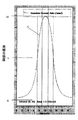
図4は、2μmの電流注入領域を有するメサ構造において、活性層の近傍で電流狭窄を行わない状態における再結合の強度分布のシミュレーション結果を示す図である。活性層において、再結合強度が最大値の50%以下になる領域は、電流注入領域よりおよそ4μm広がる。
すなわち、前記電流注入領域における電流注入経路の径をDiとし、電流狭窄領域における開口部の径をDoとするとき(図1参照)、およそ以下の関係式(1)を満たすことが望ましい。
Di<Do−4(μm)………(1)
次に、図2(d)に示すように、一旦絶縁層を除去し、絶縁層31を堆積し、メサの頂部中央付近に開口部32を形成する。
その後、図3(e)に示すように、この開口部32を含む領域に、電流注入領域8を形成したp型金属電極41を連続堆積する。
In the mesa structure light emitting device, the oxidation region of the current confinement region provided in the vicinity of the active layer is very effective in reducing the leakage current flowing through the processing surface of the mesa structure, and is an important configuration in the mesa type VCSEL. is there.
In this embodiment, the opening diameter of the current confinement portion formed in the vicinity of the active layer of the surface emitting device is determined according to the diameter of the current injection region (see FIG. 1).
Roughly, it is desirable that the oxidized region of the current confinement portion is formed in a region where the electron-hole recombination in the active layer having the structure having no current confinement portion is about 50% or less of the maximum intensity.
FIG. 4 is a diagram showing a simulation result of recombination intensity distribution in a state in which current confinement is not performed in the vicinity of the active layer in a mesa structure having a current injection region of 2 μm. In the active layer, the region where the recombination strength is 50% or less of the maximum value is expanded by about 4 μm from the current injection region.
That is, when the diameter of the current injection path in the current injection region is Di and the diameter of the opening in the current confinement region is Do (see FIG. 1), it is desirable that the following relational expression (1) is approximately satisfied.
Di <Do-4 (μm) (1)
Next, as shown in FIG. 2D, the insulating layer is once removed, and the insulating layer 31 is deposited, and an opening 32 is formed near the top center of the mesa.
Thereafter, as shown in FIG. 3E, a p-type metal electrode 41 having a
一方、図3(f)に示すように、シリコン基板51に絶縁層を形成した後、フォトリソプロセスにより、図3(e)のメサパターンに対応した金属配線パターン52を形成する。
この金属配線パターンと図3(e)の構造体とを、図3(g)に示すように対面させて接合する。
この接合には、公知技術である直接接合技術を用いることができる。
すなわち、それぞれの金属表面をクリーニングした後、接触させ、熱と圧力をかけることによって行うことができる。
On the other hand, as shown in FIG. 3F, after an insulating layer is formed on the silicon substrate 51, a metal wiring pattern 52 corresponding to the mesa pattern of FIG. 3E is formed by a photolithography process.
The metal wiring pattern and the structure shown in FIG. 3E are bonded so as to face each other as shown in FIG.
For this joining, a known direct joining technique can be used.
That is, it can be performed by cleaning each metal surface, bringing them into contact, and applying heat and pressure.
次に、GaAs基板1を公知の技術により除去する。本実施形態では、GaAs基板1の近くに積層したn型AlAs層3をフッ酸系のエッチング液により選択エッチングすることにより、GaAs基板1を除去する。
続いて、その除去面にレーザ光を出射するための開口部を有するn型電極を形成して、VCSELを完成させる。
なお、前記 配線パターンを形成したシリコン基板をVCSELの駆動に必要な回路が形成されているウエハとすることで、小型な発光装置が実現できる。このような小型発光装置は、複数の発光素子が1次元または2次元に配列する装置では非常に有用である。
Next, the
Subsequently, an n-type electrode having an opening for emitting laser light is formed on the removal surface to complete the VCSEL.
Note that a small light emitting device can be realized by using the silicon substrate on which the wiring pattern is formed as a wafer on which circuits necessary for driving the VCSEL are formed. Such a small light emitting device is very useful in an apparatus in which a plurality of light emitting elements are arranged one-dimensionally or two-dimensionally.
以上の工程で作製されたVCSELにおいて、p側電極の小さい電流注入領域から注入されたホール電流は、拡散により多少横方向に広がりながら活性層に到達するが、その電流分布の主要部は電流狭窄部の開口より小さく、電流分布は単峰性となる。
したがって、活性層で再結合によって発生する光強度分布、及び、この光が活性層の上下に存在するDBRミラーで共振するレーザ光の強度分布も、単峰性となる。
また、前述した従来例では、電流と光が電流狭窄部の開口部の周辺部に集中するのに対し、本構成では、電流狭窄部の開口部の中心部に集中するため、屈折率が大きく変化する開口部近傍の影響が小さく、利得導波型導波路となり、高次横モードを生じ難くなる。
つまり、活性層近傍に設けられた電流狭窄部によって、メサ構造の加工面を流れる漏洩電流を低減するとともに、高次横モード発振を抑制しながら基本横モードの利得を増大できるので、高出力が可能となるVCSELを得ることができる。
In the VCSEL manufactured by the above process, the hole current injected from the small current injection region of the p-side electrode reaches the active layer while spreading slightly in the lateral direction by diffusion, but the main part of the current distribution is the current confinement. It is smaller than the opening of the part, and the current distribution is unimodal.
Therefore, the light intensity distribution generated by recombination in the active layer and the intensity distribution of the laser light that resonates with the DBR mirror existing above and below the active layer are also unimodal.
In the conventional example described above, current and light are concentrated on the periphery of the opening portion of the current confinement portion, whereas in this configuration, the refractive index is large because it is concentrated on the center portion of the opening portion of the current confinement portion. The influence in the vicinity of the changing opening is small, and a gain-guided waveguide is formed, and a high-order transverse mode is hardly generated.
In other words, the current confinement part provided in the vicinity of the active layer can reduce the leakage current flowing through the processing surface of the mesa structure and increase the fundamental transverse mode gain while suppressing higher-order transverse mode oscillation, so that high output is achieved. A possible VCSEL can be obtained.
なお、p側の注入領域を形成する金属電極が活性層で発生した光を反射するため、p側の多層膜反射ミラーの反射率が低くても、レーザ発振に必要な反射が得られるので、多層膜の層数を減らすことが可能である。
また、この金属電極の反射ミラーは波長依存性が小さいので、この構成により、多層膜ミラーの波長依存性が軽減できる。
また、上記した本実施の形態の製造方法によれば、ウエハプロセスでの製造が可能となり、量産に適した製造方法を実現することができる。
In addition, since the metal electrode forming the p-side injection region reflects the light generated in the active layer, the reflection necessary for laser oscillation can be obtained even when the reflectivity of the p-side multilayer mirror is low. It is possible to reduce the number of layers of the multilayer film.
In addition, since the reflection mirror of the metal electrode has a small wavelength dependency, this configuration can reduce the wavelength dependency of the multilayer mirror.
Further, according to the manufacturing method of the present embodiment described above, manufacturing by a wafer process becomes possible, and a manufacturing method suitable for mass production can be realized.
つぎに、本発明の本実施例における面発光レーザの製造方法について説明する。
本実施例の面発光レーザの製造方法は、基本的には上記した本発明の実施形態のものと変わらないので、本発明の実施形態で用いた図2及び図3を用いて説明する。
まず、最初の工程において、GaAs基板1上に公知の技術であるMOCVD法により、各層を順次成長させる。
すなわち、n型GaAsバッファ層2、n型AlAs層3、n型Al0.25Ga0.75As層4、n型DBR−1層、活性領域5、p型AlAs層6、p型DBR−2層、およびp型コンタクト層7を、順次成長させる(図2(a))。n型DBR−1層は、Al0.8Ga0.2AsとAl0.2Ga0.8Asとを各層の膜厚がλ/4nr(ただし、λはレ−ザの発振波長、nrは構成する媒質の屈折率)となるように交互に29.5周期積層した積層体である。
活性領域は、アンドープのAl0.1Ga0.89Asよりなる量子井戸層と、アンドープのAl0.2Ga0.8Asよりなる障壁層と、これらの量子構造を挟むアンドープのAl0.25Ga0.75Asよりなるスペーサ層で構成される。
p型AlAs層6は、後に水蒸気により酸化処理が行われ、電流狭窄領域を形成する層である。
p型DBR−2層は、Al0.8Ga0.2AsとAl0.2Ga0.8Asとを各層の膜厚がλ/4nrとなるように交互に40.5周期積層した積層体である。
p型コンタクト層7は、金属電極を形成することでオーミックコンタクトを得るため、高キャリヤ濃度である。
Next, a method for manufacturing the surface emitting laser according to this embodiment of the present invention will be described.
The surface emitting laser manufacturing method of this example is basically the same as that of the above-described embodiment of the present invention, and will be described with reference to FIGS. 2 and 3 used in the embodiment of the present invention.
First, in the first step, each layer is sequentially grown on the
An n-type
The active region includes a quantum well layer made of undoped Al0.1Ga0.89As, a barrier layer made of undoped Al0.2Ga0.8As, and a spacer layer made of undoped Al0.25Ga0.75As sandwiching these quantum structures. Is done.
The p-type AlAs
p-type DBR-2 layers, a laminate thickness of each layer and the Al0.8Ga0.2As and Al0.2Ga0.8As was 40.5 cycles alternately stacked so that the lambda / 4n r.
The p-
次に、基板上に、前記電流狭窄領域を形成するための層を含むメサ構造の面発光レーザパターンを形成する。
基板上面にSiON膜を堆積した後、レジストパターン21を形成し、このパターンをマスクに、公知のエッチング技術により、少なくともAlAs層6が露出するまでエッチングを行って30μm径のメサ形状を形成した後、レジストを除去する(図2(b))。
Next, a mesa structure surface emitting laser pattern including a layer for forming the current confinement region is formed on the substrate.
After depositing a SiON film on the upper surface of the substrate, a resist pattern 21 is formed, and etching is performed by using a known etching technique until at least the AlAs
次に、前記電流狭窄領域を形成するための層の周辺部を酸化して活性層に電流を注入する経路となる開口部を有する電流狭窄領を形成する。
公知技術であるウエット酸化により、前記露出しているAlAs層6をメサ形状の周囲からを選択的に酸化させ、酸化領域に囲まれた非酸化領域(開口部)を形成する。
これにより、活性領域の近傍に活性層への電流パスとなる開口部を有する電流狭窄部を形成する(図2(c))。
Next, a current confinement region having an opening serving as a path for injecting current into the active layer is formed by oxidizing the peripheral portion of the layer for forming the current confinement region.
The exposed AlAs
Thereby, a current confinement portion having an opening serving as a current path to the active layer is formed in the vicinity of the active region (FIG. 2C).
次に、前記メサ構造の頂部中央に、電流注入経路の径が前記電流狭窄領域の開口部の径よりも小さい径を備えた電流注入領域を、前記活性層を挟んで光出射側と反対側に形成する工程において、つぎのように電流注入領域を形成する。
SiON膜を除去し、全面にSiN保護膜(絶縁層)31を堆積した後、円柱の頂部のほぼ中央付近に10μm径の円形の窓(開口部)32を開け(図2(d))、p型金属電極41となるTi、Au を連続堆積する(図3(e))。
Next, at the center of the top of the mesa structure, a current injection region having a diameter of a current injection path smaller than the diameter of the opening of the current confinement region is disposed on the side opposite to the light emitting side with the active layer interposed therebetween. In the step of forming, the current injection region is formed as follows.
After removing the SiON film and depositing a SiN protective film (insulating layer) 31 on the entire surface, a circular window (opening) 32 having a diameter of 10 μm is opened near the center of the top of the cylinder (FIG. 2D). Ti and Au to be the p-type metal electrode 41 are continuously deposited (FIG. 3E).
一方、前記電流注入領域を形成した後、該電流注入領域を形成した面を配線パターンが形成された別基板に対面させて接合する工程において、これらをつぎのように対面させて接合させる(図3(g))。
表面にAuが露出した配線パターン52を有するシリコン基板51を別途準備し、この金属配線パターンと図3(e)の構造体を、対面させで接合させる。
接合は、それぞれの金表面をクリーニングした後、接触させ、熱と圧力をかける直接接合によって行う(図3(f))。
On the other hand, after forming the current injection region, in the step of facing and bonding the surface on which the current injection region is formed to another substrate on which the wiring pattern is formed, these are faced and bonded as follows (FIG. 3 (g)).
A silicon substrate 51 having a wiring pattern 52 with Au exposed on the surface is prepared separately, and the metal wiring pattern and the structure shown in FIG.
Bonding is performed by direct bonding after cleaning the respective gold surfaces and then applying heat and pressure (FIG. 3 (f)).
次に、前記電流注入領域を形成した面を配線パターンが形成された別基板に対面させて接合した後、面発光レーザパターンを形成する工程で用いた前記基板を除去する工程において、GaAs基板1を公知の技術により除去する。
本実施例では、GaAs基板1の近くに積層したn型AlAs層3をフッ酸系のエッチング液により選択エッチングすることにより、GaAs基板1を除去する手法を用いた。
続いて、その除去面にレーザ光を出射するための開口部を有するn型電極を形成して、VCSELを完成させる。
Next, in the step of removing the substrate used in the step of forming the surface emitting laser pattern after bonding the surface on which the current injection region is formed facing another substrate on which the wiring pattern is formed, the
In this embodiment, a method of removing the
Subsequently, an n-type electrode having an opening for emitting laser light is formed on the removal surface to complete the VCSEL.
本実施例の構成によれば、基本横モード発振で高出力が得られると供に、放熱性に優れるので、アレイ形態での隣接素子間の相互干渉が小さく、実装が容易で、発光装置を小型化することができる。
また、これにより、アレイで使用される複写機やプリンタのレーザスキャナーの光源に適した面発光レーザを実現することができる。
According to the configuration of this embodiment, high output is obtained by basic transverse mode oscillation and excellent heat dissipation, so that mutual interference between adjacent elements in the array form is small, mounting is easy, and the light emitting device is It can be downsized.
This also makes it possible to realize a surface emitting laser suitable for a light source of a laser scanner of a copying machine or a printer used in the array.
1:GaAs基板
2:バッファ層
3:n型AlAs層(AlAs分離層)
4:n型AlxGa1−xAs層(電流拡散層)
5:活性領域(活性層)
6:AlAs電流狭窄領域(p型AlAs層)
7:p型コンタクト層
8:電流注入領域
21:VCSELパターン
31:絶縁層
32:開口部
41:p型金属電極
51:シリコン基板
52:金属配線
61:n型金属電極
62:光放射用窓
1: GaAs substrate 2: buffer layer 3: n-type AlAs layer (AlAs separation layer)
4: n-type AlxGa1-xAs layer (current diffusion layer)
5: Active region (active layer)
6: AlAs current confinement region (p-type AlAs layer)
7: p-type contact layer 8: current injection region 21: VCSEL pattern 31: insulating layer 32: opening 41: p-type metal electrode 51: silicon substrate 52: metal wiring 61: n-type metal electrode 62: light emission window
Claims (11)
前記活性層を挟んで光出射側と反対側に設けられた電流注入領域を備え、
前記電流注入領域における電流注入経路の径が、前記開口部の径よりも小さい径によって構成されていることを特徴とする面発光レーザ。 A surface emitting laser having an opening serving as a path for injecting current into an active layer and having a current confinement region provided around the opening,
A current injection region provided on the side opposite to the light emitting side across the active layer,
A surface emitting laser characterized in that a diameter of a current injection path in the current injection region is configured to be smaller than a diameter of the opening.
Di<Do−4(μm)………(1) 3. The surface according to claim 1, wherein when the diameter of the current injection path in the current injection region is Di and the diameter of the opening is Do, the following relational expression (1) is satisfied. Light emitting laser.
Di <Do-4 (μm) (1)
基板上に、前記電流狭窄領域を形成するための層を含むメサ構造の面発光レーザパターンを形成する工程と、
前記電流狭窄領域を形成するための層に、活性層に注入する電流の経路となる開口部を備え、該開口部の周辺を絶縁化して電流狭窄領域を形成する工程と、
前記メサ構造の頂部中央に、電流注入経路の径が前記電流狭窄領域の開口部の径よりも小さい径を備えた電流注入領域を、前記活性層を挟んで光出射側と反対側に形成する工程と、
を有することを特徴とする面発光レーザの製造方法。 A method of manufacturing a surface-emitting laser having a current confinement region having an opening serving as a path for injecting a current into an active layer,
Forming a surface emitting laser pattern having a mesa structure including a layer for forming the current confinement region on the substrate;
Forming a current confinement region in the layer for forming the current confinement region, comprising an opening serving as a path for a current to be injected into the active layer, and insulating the periphery of the opening;
At the center of the top of the mesa structure, a current injection region having a diameter of a current injection path smaller than the diameter of the opening of the current confinement region is formed on the side opposite to the light emitting side with the active layer interposed therebetween. Process,
A method for manufacturing a surface emitting laser, comprising:
前記電流注入領域を形成した面を配線パターンが形成された別基板に対面させて接合する工程で用いる基板がシリコン基板であることを特徴とする請求項9または請求項10に記載の面発光レーザの製造方法。 The substrate used in the step of forming the surface emitting laser pattern having the mesa structure is a GaAs substrate,
11. The surface emitting laser according to claim 9, wherein a substrate used in the step of bonding the surface on which the current injection region is formed to another substrate on which a wiring pattern is formed is a silicon substrate. Manufacturing method.
Priority Applications (3)
| Application Number | Priority Date | Filing Date | Title |
|---|---|---|---|
| JP2007171579A JP2009010248A (en) | 2007-06-29 | 2007-06-29 | Surface emitting laser and method of manufacturing the same |
| US12/143,337 US7813402B2 (en) | 2007-06-29 | 2008-06-20 | Surface emitting laser and method of manufacturing the same |
| CN2008101317691A CN101350499B (en) | 2007-06-29 | 2008-06-27 | Surface emitting laser and method of manufacturing the same |
Applications Claiming Priority (1)
| Application Number | Priority Date | Filing Date | Title |
|---|---|---|---|
| JP2007171579A JP2009010248A (en) | 2007-06-29 | 2007-06-29 | Surface emitting laser and method of manufacturing the same |
Publications (2)
| Publication Number | Publication Date |
|---|---|
| JP2009010248A true JP2009010248A (en) | 2009-01-15 |
| JP2009010248A5 JP2009010248A5 (en) | 2010-08-12 |
Family
ID=40160441
Family Applications (1)
| Application Number | Title | Priority Date | Filing Date |
|---|---|---|---|
| JP2007171579A Pending JP2009010248A (en) | 2007-06-29 | 2007-06-29 | Surface emitting laser and method of manufacturing the same |
Country Status (3)
| Country | Link |
|---|---|
| US (1) | US7813402B2 (en) |
| JP (1) | JP2009010248A (en) |
| CN (1) | CN101350499B (en) |
Families Citing this family (13)
| Publication number | Priority date | Publication date | Assignee | Title |
|---|---|---|---|---|
| JP4537658B2 (en) * | 2002-02-22 | 2010-09-01 | 株式会社リコー | Surface emitting laser element, surface emitting laser array using the surface emitting laser element, electrophotographic system, surface emitting laser module, optical communication system, optical interconnection system, and surface emitting laser element manufacturing method |
| JP5355276B2 (en) | 2009-07-28 | 2013-11-27 | キヤノン株式会社 | Surface emitting laser |
| KR20110085609A (en) * | 2010-01-21 | 2011-07-27 | 엘지이노텍 주식회사 | Light emitting device and method for fabricating the same |
| JP2012248795A (en) * | 2011-05-31 | 2012-12-13 | Toshiba Corp | Semiconductor light-emitting element and method of manufacturing the same |
| KR20130062969A (en) * | 2013-05-24 | 2013-06-13 | 한국전자통신연구원 | Vertical cavity surface emitting laser using wafer bonding process and method of fabricating the same |
| US9728934B2 (en) * | 2015-08-31 | 2017-08-08 | Avago Technologies General Ip (Singapore) Pte. Ltd. | Back-side-emitting vertical cavity surface emitting laser (VCSEL) wafer bonded to a heat-dissipation wafer, devices and methods |
| JP6705151B2 (en) * | 2015-10-27 | 2020-06-03 | セイコーエプソン株式会社 | Atomic oscillator |
| US10971890B2 (en) * | 2016-12-05 | 2021-04-06 | Goertek, Inc. | Micro laser diode transfer method and manufacturing method |
| CN109923468A (en) * | 2016-12-05 | 2019-06-21 | 歌尔股份有限公司 | Micro- laser diode display device and electronic equipment |
| US10454243B2 (en) | 2017-02-28 | 2019-10-22 | Avago Technologies International Sales Pte. Limited | Light source driver circuit that uses a low supply voltage and is capable of operating at a high bandwidth |
| US10833483B2 (en) * | 2017-12-07 | 2020-11-10 | Lumentum Operations Llc | Emitter array having structure for submount attachment |
| KR102117084B1 (en) * | 2018-08-20 | 2020-06-01 | 광전자 주식회사 | Highly efficient oxidation-type VCSEL with improved light extraction and method for manufacturing thereof |
| US20220416509A1 (en) * | 2019-12-20 | 2022-12-29 | Sony Semiconductor Solutions Corporation | Light emitting device and method of manufacturing light emitting device |
Citations (4)
| Publication number | Priority date | Publication date | Assignee | Title |
|---|---|---|---|---|
| JP2001251016A (en) * | 1999-12-28 | 2001-09-14 | Canon Inc | Surface emitting semiconductor laser and its manufacturing method |
| JP2002196571A (en) * | 2000-12-26 | 2002-07-12 | Canon Inc | Image forming device |
| JP2004288902A (en) * | 2003-03-24 | 2004-10-14 | Sony Corp | Surface emitting laser element and its manufacturing method |
| JP2006114915A (en) * | 2004-10-14 | 2006-04-27 | Samsung Electronics Co Ltd | Vecsel of funnel structure |
Family Cites Families (12)
| Publication number | Priority date | Publication date | Assignee | Title |
|---|---|---|---|---|
| EP0495301A1 (en) * | 1990-12-14 | 1992-07-22 | AT&T Corp. | Method for making a semiconductor laser |
| US6075802A (en) * | 1998-03-12 | 2000-06-13 | Telefonaktiebolaget L, Ericsson | Lateral confinement laser |
| US7881359B2 (en) * | 1999-04-23 | 2011-02-01 | The Furukawa Electric Co., Ltd | Surface-emission semiconductor laser device |
| US6529541B1 (en) | 2000-11-13 | 2003-03-04 | Fuji Xerox Co., Ltd. | Surface emitting semiconductor laser |
| JP2002208755A (en) | 2000-11-13 | 2002-07-26 | Fuji Xerox Co Ltd | Surface emitting semiconductor laser |
| US6650683B2 (en) * | 2000-11-20 | 2003-11-18 | Fuji Xerox Co, Ltd. | Surface emitting semiconductor laser |
| US6791119B2 (en) * | 2001-02-01 | 2004-09-14 | Cree, Inc. | Light emitting diodes including modifications for light extraction |
| US6589805B2 (en) * | 2001-03-26 | 2003-07-08 | Gazillion Bits, Inc. | Current confinement structure for vertical cavity surface emitting laser |
| US7016392B2 (en) * | 2003-04-30 | 2006-03-21 | Ashish Tandon | GaAs-based long-wavelength laser incorporating tunnel junction structure |
| JP5376104B2 (en) * | 2005-07-04 | 2013-12-25 | ソニー株式会社 | Surface emitting semiconductor laser |
| WO2007103527A2 (en) * | 2006-03-07 | 2007-09-13 | Brenner Mary K | Red light laser |
| JP4872987B2 (en) * | 2008-08-25 | 2012-02-08 | ソニー株式会社 | Surface emitting semiconductor laser |
-
2007
- 2007-06-29 JP JP2007171579A patent/JP2009010248A/en active Pending
-
2008
- 2008-06-20 US US12/143,337 patent/US7813402B2/en not_active Expired - Fee Related
- 2008-06-27 CN CN2008101317691A patent/CN101350499B/en not_active Expired - Fee Related
Patent Citations (4)
| Publication number | Priority date | Publication date | Assignee | Title |
|---|---|---|---|---|
| JP2001251016A (en) * | 1999-12-28 | 2001-09-14 | Canon Inc | Surface emitting semiconductor laser and its manufacturing method |
| JP2002196571A (en) * | 2000-12-26 | 2002-07-12 | Canon Inc | Image forming device |
| JP2004288902A (en) * | 2003-03-24 | 2004-10-14 | Sony Corp | Surface emitting laser element and its manufacturing method |
| JP2006114915A (en) * | 2004-10-14 | 2006-04-27 | Samsung Electronics Co Ltd | Vecsel of funnel structure |
Also Published As
| Publication number | Publication date |
|---|---|
| CN101350499A (en) | 2009-01-21 |
| US20090003401A1 (en) | 2009-01-01 |
| US7813402B2 (en) | 2010-10-12 |
| CN101350499B (en) | 2010-07-21 |
Similar Documents
| Publication | Publication Date | Title |
|---|---|---|
| JP2009010248A (en) | Surface emitting laser and method of manufacturing the same | |
| US7869483B2 (en) | Surface emitting laser | |
| JP4352337B2 (en) | Semiconductor laser and semiconductor laser device | |
| JP4347369B2 (en) | Manufacturing method of surface emitting laser | |
| JPH0669585A (en) | Surface emitting semiconductor laser and its manufacture | |
| JP4760380B2 (en) | Surface emitting laser | |
| JP4878322B2 (en) | Surface emitting laser element and method for manufacturing surface emitting laser element | |
| JP2002353563A (en) | Semiconductor light-emitting element and manufacturing method therefor | |
| WO2021117411A1 (en) | Surface-emitting laser, surface-emitting laser array, electronic apparatus, and production method for surface-emitting laser | |
| JP5190038B2 (en) | Surface emitting laser | |
| JP5590829B2 (en) | Surface emitting laser, surface emitting laser array, and image forming apparatus | |
| JP2009259857A (en) | Surface emitting laser element and surface emitting laser element array | |
| US7286584B2 (en) | Carrier bonded 1550 nm VCSEL with InP substrate removal | |
| JP6252222B2 (en) | Surface emitting laser array and laser apparatus | |
| JP5005937B2 (en) | Surface emitting laser element | |
| JP4024471B2 (en) | Surface emitting semiconductor laser | |
| JP5006242B2 (en) | Surface emitting semiconductor laser device | |
| JP2007087994A (en) | Surface-emitting semiconductor laser element | |
| WO2021124967A1 (en) | Vertical cavity surface-emitting laser element, vertical cavity surface-emitting laser element array, vertical cavity surface-emitting laser module, and method for manufacturing vertical cavity surface-emitting laser element | |
| JP2004281968A (en) | Surface-emitting semiconductor laser element | |
| US7885312B2 (en) | Surface emitting semiconductor laser element | |
| JP2009170508A (en) | Surface-emitting semiconductor laser and manufacturing method thereof | |
| JP2007227860A (en) | Semiconductor light-emitting device | |
| JP2007129010A (en) | Surface-emitting semiconductor laser and method of manufacturing same | |
| JP2004146515A (en) | Semiconductor laser element |
Legal Events
| Date | Code | Title | Description |
|---|---|---|---|
| A521 | Written amendment |
Free format text: JAPANESE INTERMEDIATE CODE: A523 Effective date: 20100629 |
|
| A621 | Written request for application examination |
Free format text: JAPANESE INTERMEDIATE CODE: A621 Effective date: 20100629 |
|
| A131 | Notification of reasons for refusal |
Free format text: JAPANESE INTERMEDIATE CODE: A131 Effective date: 20111004 |
|
| A977 | Report on retrieval |
Free format text: JAPANESE INTERMEDIATE CODE: A971007 Effective date: 20111005 |
|
| A02 | Decision of refusal |
Free format text: JAPANESE INTERMEDIATE CODE: A02 Effective date: 20120214 |