JP2008545501A - Backing block for ultrasonic sensor assembly - Google Patents
Backing block for ultrasonic sensor assembly Download PDFInfo
- Publication number
- JP2008545501A JP2008545501A JP2008515354A JP2008515354A JP2008545501A JP 2008545501 A JP2008545501 A JP 2008545501A JP 2008515354 A JP2008515354 A JP 2008515354A JP 2008515354 A JP2008515354 A JP 2008515354A JP 2008545501 A JP2008545501 A JP 2008545501A
- Authority
- JP
- Japan
- Prior art keywords
- auxiliary
- component
- base
- base component
- backing block
- Prior art date
- Legal status (The legal status is an assumption and is not a legal conclusion. Google has not performed a legal analysis and makes no representation as to the accuracy of the status listed.)
- Pending
Links
- 238000012545 processing Methods 0.000 claims abstract description 31
- 239000000853 adhesive Substances 0.000 claims description 31
- 230000001070 adhesive effect Effects 0.000 claims description 31
- 238000000034 method Methods 0.000 claims description 21
- 238000002604 ultrasonography Methods 0.000 claims description 10
- 238000003384 imaging method Methods 0.000 claims description 7
- 230000008569 process Effects 0.000 claims description 7
- 239000000523 sample Substances 0.000 claims description 4
- 230000003111 delayed effect Effects 0.000 claims description 2
- 230000008878 coupling Effects 0.000 claims 2
- 238000010168 coupling process Methods 0.000 claims 2
- 238000005859 coupling reaction Methods 0.000 claims 2
- 239000007787 solid Substances 0.000 claims 1
- 238000012285 ultrasound imaging Methods 0.000 abstract description 13
- 239000011295 pitch Substances 0.000 description 8
- 230000008901 benefit Effects 0.000 description 6
- 230000005540 biological transmission Effects 0.000 description 6
- 238000013459 approach Methods 0.000 description 5
- 238000005516 engineering process Methods 0.000 description 5
- 238000013461 design Methods 0.000 description 4
- 239000004593 Epoxy Substances 0.000 description 3
- 230000003321 amplification Effects 0.000 description 3
- 230000000712 assembly Effects 0.000 description 3
- 238000000429 assembly Methods 0.000 description 3
- 238000004891 communication Methods 0.000 description 3
- 239000004020 conductor Substances 0.000 description 3
- 238000004519 manufacturing process Methods 0.000 description 3
- 238000003199 nucleic acid amplification method Methods 0.000 description 3
- 230000002093 peripheral effect Effects 0.000 description 3
- 238000003491 array Methods 0.000 description 2
- 238000012937 correction Methods 0.000 description 2
- 230000003993 interaction Effects 0.000 description 2
- 230000004075 alteration Effects 0.000 description 1
- 238000010276 construction Methods 0.000 description 1
- 230000001419 dependent effect Effects 0.000 description 1
- 238000009826 distribution Methods 0.000 description 1
- 230000002349 favourable effect Effects 0.000 description 1
- PCHJSUWPFVWCPO-UHFFFAOYSA-N gold Chemical compound [Au] PCHJSUWPFVWCPO-UHFFFAOYSA-N 0.000 description 1
- 239000010931 gold Substances 0.000 description 1
- 229910052737 gold Inorganic materials 0.000 description 1
- 238000007654 immersion Methods 0.000 description 1
- 230000006872 improvement Effects 0.000 description 1
- 238000010348 incorporation Methods 0.000 description 1
- 238000001764 infiltration Methods 0.000 description 1
- 230000008595 infiltration Effects 0.000 description 1
- 238000007689 inspection Methods 0.000 description 1
- 239000000463 material Substances 0.000 description 1
- 238000002493 microarray Methods 0.000 description 1
- 238000012986 modification Methods 0.000 description 1
- 230000004048 modification Effects 0.000 description 1
- 238000005457 optimization Methods 0.000 description 1
- 238000013021 overheating Methods 0.000 description 1
- 238000005192 partition Methods 0.000 description 1
- 238000007747 plating Methods 0.000 description 1
- 238000000926 separation method Methods 0.000 description 1
- 229910000679 solder Inorganic materials 0.000 description 1
Images


Classifications
-
- B—PERFORMING OPERATIONS; TRANSPORTING
- B06—GENERATING OR TRANSMITTING MECHANICAL VIBRATIONS IN GENERAL
- B06B—METHODS OR APPARATUS FOR GENERATING OR TRANSMITTING MECHANICAL VIBRATIONS OF INFRASONIC, SONIC, OR ULTRASONIC FREQUENCY, e.g. FOR PERFORMING MECHANICAL WORK IN GENERAL
- B06B1/00—Methods or apparatus for generating mechanical vibrations of infrasonic, sonic, or ultrasonic frequency
- B06B1/02—Methods or apparatus for generating mechanical vibrations of infrasonic, sonic, or ultrasonic frequency making use of electrical energy
- B06B1/06—Methods or apparatus for generating mechanical vibrations of infrasonic, sonic, or ultrasonic frequency making use of electrical energy operating with piezoelectric effect or with electrostriction
- B06B1/0607—Methods or apparatus for generating mechanical vibrations of infrasonic, sonic, or ultrasonic frequency making use of electrical energy operating with piezoelectric effect or with electrostriction using multiple elements
- B06B1/0622—Methods or apparatus for generating mechanical vibrations of infrasonic, sonic, or ultrasonic frequency making use of electrical energy operating with piezoelectric effect or with electrostriction using multiple elements on one surface
Abstract
トランスデューサアレイ12と、前記トランスデューサアレイ12を超音波撮像システムのメインシステムの処理ユニットに接続する相互接続ケーブル18とを相互接続するバッキングブロック16であり、このバッキングブロック16は、前記相互接続ケーブル18に電気接続され、相互接続構造28のパターンを設けた少なくとも1つのベース電子部品24、一方の側面40において前記ベース部品24に電気結合され、対向する側面38において前記トランスデューサアレイ12に接続される再分配インターポーザ22、及び前記ベース部品24により支持される少なくとも1つの補助電子部品26を有する。再分配インターポーザ22は、トランスデューサアレイ12に接続される前記側面38よりも、前記ベース部品24に接続される側面のピッチの方が小さくなるように、少なくとも1次元において先細りしているので、前記補助部品26は、再分配インターポーザ22に沿って、すなわち再分配インターポーザ22とベース部品24との共通面上に配される。 A backing block 16 interconnects the transducer array 12 and an interconnect cable 18 that connects the transducer array 12 to a processing unit of the main system of the ultrasound imaging system. The backing block 16 is connected to the interconnect cable 18. At least one base electronic component 24 that is electrically connected and provided with a pattern of interconnect structure 28, electrically coupled to the base component 24 on one side 40 and connected to the transducer array 12 on the opposite side 38. It has an interposer 22 and at least one auxiliary electronic component 26 supported by the base component 24. The redistribution interposer 22 tapers in at least one dimension so that the pitch of the side surface connected to the base component 24 is smaller than the side surface 38 connected to the transducer array 12, so that the auxiliary The component 26 is disposed along the redistribution interposer 22, that is, on the common surface of the redistribution interposer 22 and the base component 24.
Description
本発明は一般的に、超音波撮像システム、特に超音波トランスデューサアレイ用のバッキングブロック(backing block)、並びに超音波撮像システムにおける超音波トランスデューサアレイに送信及びこのアレイにより受信される信号を処理する方法に関する。 The present invention generally relates to an ultrasound imaging system, particularly a backing block for an ultrasound transducer array, and a method for processing signals transmitted to and received by the ultrasound transducer array in an ultrasound imaging system. About.
本発明は、トランスデューサアレイ及びハイブリッドマイクロビーム形成部を含むバッキングブロックを有する超音波センサ組立体にも関し、このハイブリッドマイクロビーム形成部は、トランスデューサアレイをメインの超音波撮像システムの処理ユニットにつながっている相互接続ケーブルに接続する。 The present invention also relates to an ultrasonic sensor assembly having a backing block including a transducer array and a hybrid microbeamformer, the hybrid microbeamformer connecting the transducer array to a main ultrasound imaging system processing unit. Connect to the interconnect cable that is present.
超音波撮像システムにおいて、トランスデューサアレイは一般的に超音波又は音波を送受信するために用いられる。ボリューム画像、すなわち略三次元の関心領域の問い合わせ(interrogation)は、多次元(multi-D)トランスデューサアレイ、例えばトランスデューサエレメントの二次元アレイを使用することにより得られる。 In an ultrasound imaging system, a transducer array is generally used to transmit and receive ultrasound or sound waves. Volume images, or interrogation of approximately three-dimensional regions of interest, can be obtained by using a multi-D transducer array, eg, a two-dimensional array of transducer elements.
ある形式の超音波トランスデューサの設計において、トランスデューサエレメントはASIC(application specific integrated circuit)の表面に取り付けられ、個々に電気接続される。このASICはしばしばマイクロビーム形成部と呼ばれ、例えばビーム形成、信号増幅等をするためのトランスデューサエレメントの電気制御を備え、超音波撮像システムのトランスデューサエレメントと信号処理チャンネルとの間を相互接続ケーブルを介して連係させる。 In one type of ultrasonic transducer design, the transducer elements are attached to the surface of an ASIC (application specific integrated circuit) and are individually electrically connected. This ASIC is often referred to as a microbeamformer, and includes electrical control of the transducer elements, for example, beamforming, signal amplification, etc., and interconnecting cables between the transducer elements of the ultrasound imaging system and signal processing channels. Work through.
マイクロビーム形成部を備える多次元トランスデューサアレイの実用的な実装は、性能、電力損失、フォームファクタ、市場に出すまでの費用及び時間に関し多くのトレードオフ(tradeoff)を必要とする。ある特定のトレードオフの組は、ASICの設計、及びASICをトランスデューサエレメントに接続する相互接続構造との関係の周りを回っている。"フリップチップ"相互接続を用いた幾何学的に制限されたピッチ整合したASIC、及び"フレックスインバッキング(flex in backing)"相互接続を用いた幾何学的に制限されていないASICのような2つの手法が今まで考えられてきた。 Practical implementations of multi-dimensional transducer arrays with microbeamformers require many tradeoffs regarding performance, power loss, form factor, cost to market and time. One particular set of tradeoffs goes around the relationship between the ASIC design and the interconnect structure that connects the ASIC to the transducer elements. 2 such as geometrically limited pitch-matched ASICs using “flip chip” interconnects and non-geometrically limited ASICs using “flex in backing” interconnects Two approaches have been considered so far.
はんだボールのような小さな導電バンプを用いた電気相互接続に基づくフリップチップ手法は、低電力、スモールフォームファクタ、低コスト及び低い複雑性の利点を持つが、再利用を制限し、もしあれば、相互接続構造内における望まない音響的相互作用により、画像アーチファクトの影響を受けやすくなる。他方、"フレックスインバッキング"手法は、良好な潜在性能及びASICの再利用の利点を持つが、分厚く、複雑で及びコストがかかる欠点がある。本発明は、これらフリップチップ手法及びフレックスインバッキング手法の両方の欠点を克服しようとしている。 The flip chip approach based on electrical interconnections using small conductive bumps such as solder balls has the advantages of low power, small form factor, low cost and low complexity but limits reuse and, if any, Undesirable acoustic interactions within the interconnect structure are susceptible to image artifacts. On the other hand, the “flex-backing” approach has good potential performance and ASIC reuse advantages, but has the disadvantages of being thick, complex and costly. The present invention seeks to overcome the drawbacks of both these flip chip and flex-in backing approaches.
典型的なフリップチップアーキテクチャを用いた相互接続構造において、撮像応用に合わせられたマイクロビーム形成部は、音響アパーチャと同じサイズであり、前記アレイのピッチにピッチ整合したセルで構成される。このサイズの限度内で必要な機能及び性能の全てを提供することは、極めて挑戦的であり、かなりの妥協を必要とする。これら妥協は、減少した浸透の費用でのトランスデューサハウジングにある利用可能な空間に嵌合するさらに細かい形状を用いた低電圧ASIC処理を使用すること、及び(前記ピッチ整合から生じる)ASICを再利用する能力の殆ど削除を含んでいる。他の妥協は、トランスデューサハウジングにある限られた空間は、必要に応じて、妥協及び近似を用いて、ASICの最低限の機能を実施するためだけに、圧力の増加をもたらす。その上、ASICのセルが各トランスデューサエレメントよりも下に置かれるので、ASICはマイクロビーム形成部を介して完全に混合したアナログ及びデジタル機能部品の両方を有する。 In an interconnect structure using a typical flip-chip architecture, the microbeamformer tailored for imaging applications is the same size as the acoustic aperture and consists of cells that are pitch matched to the pitch of the array. Providing all of the necessary functions and performance within this size limit is extremely challenging and requires considerable compromise. These compromises include using a low voltage ASIC process with a finer shape that fits into the available space in the transducer housing at reduced infiltration costs and reusing the ASIC (resulting from said pitch matching). Includes most of the ability to delete. Another compromise is that the limited space in the transducer housing results in an increase in pressure only to perform the minimum function of the ASIC, using compromises and approximations, if necessary. In addition, since the ASIC cell is placed below each transducer element, the ASIC has both analog and digital functional components fully mixed through the microbeamformer.
フリップチップ手法の大幅なASIC制限は、ビーム形成電子機器がトランスデューサアレイの領域内になければならないことである。残念なことに、この制約はしばしば、画像の品質を落とす又は画像アーチファクトを生じさせる最適化及び性能のトレードオフとなる。加えて、熱がトランスデューサアレイを介してより直接的に患者に移り、さらに厳しい電力要件となる。 A significant ASIC limitation of the flip chip approach is that the beam forming electronics must be in the area of the transducer array. Unfortunately, this constraint is often an optimization and performance trade-off that degrades image quality or creates image artifacts. In addition, heat is transferred to the patient more directly through the transducer array, creating even more stringent power requirements.
フレックスインバッキング手法を使用した相互接続は、米国特許公開番号20030085635に一般的に開示され、ここで参照することにより取り入れられ、接着剤を用いて一緒に張り合わされたバッキング材料からなるプレートと、フレックス回路との交互の層から、導電性バッキングブロック組立体を構成することを含む。この組立体は、トランスデューサエレメントに接続された上面がトランスデューサエレメントの下面に取り付けるための滑らかな仕上げ、好ましくは金メッキに接地されるように、過熱圧迫の圧力下で硬化する。導電性バッキングブロック組立体をトランスデューサエレメントに接続するある方法は、低い粘性の接着剤、例えばエポキシを用いた接着取り付けにより接続される。 An interconnection using a flex-in backing technique is generally disclosed in U.S. Patent Publication No. 20030085635, incorporated by reference herein, a plate of backing material bonded together with an adhesive, and a flex Constructing a conductive backing block assembly from alternating layers with circuitry. The assembly is cured under pressure of overheating so that the upper surface connected to the transducer element is grounded to a smooth finish, preferably gold plating, for attachment to the lower surface of the transducer element. One method of connecting the conductive backing block assembly to the transducer element is connected by adhesive attachment using a low viscosity adhesive, such as an epoxy.
小さなサイズのトランスデューサハウジング内に嵌合することを可能にするために、これにより形成されるバッキングブロックに最小のサイズを供給する、複数の電子部品で構成されるマイクロビーム形成部にトランスデューサアレイのトランスデューサエレメントを接続するための相互接続構造を持つことが望ましく、さらに高電圧、改良された機能及び優れた性能も可能にすることが望ましい。 Transducer array transducers in a microbeamformer composed of multiple electronic components that provide a minimum size to the backing block formed thereby to allow fitting within a small size transducer housing It is desirable to have an interconnect structure for connecting the elements, and also to enable high voltage, improved functionality and superior performance.
本発明の目的は、新規及び改良された超音波撮像システム、特に多次元トランスデューサアレイ及びマイクロビーム形成部を含む、このシステム用の超音波センサ組立体を提供することである。 It is an object of the present invention to provide a new and improved ultrasonic imaging system, in particular an ultrasonic sensor assembly for this system, including a multidimensional transducer array and a microbeamformer.
本発明の他の目的は、アナログ及びデジタル機能が特定の目的のために最適化された別個の電子部品により実行される超音波撮像システム用の新規及び改良されたマイクロビーム形成部を提供することである。 Another object of the present invention is to provide a new and improved microbeamformer for ultrasound imaging systems in which analog and digital functions are performed by separate electronic components optimized for a particular purpose. It is.
本発明の他の目的は、トランスデューサアレイのトランスデューサエレメントと、メインの超音波撮像システムの処理ユニットに接続される1つ以上の相互接続ケーブルとの間に接続を提供する、バッキングブロックと呼ばれる超音波撮像システム用の新しい相互接続構造を提供することである。 Another object of the present invention is an ultrasound called a backing block that provides a connection between the transducer elements of the transducer array and one or more interconnect cables connected to the processing unit of the main ultrasound imaging system. It is to provide a new interconnect structure for an imaging system.
本発明のさらに他の目的は、超音波撮像システムにおけるトランスデューサアレイのトランスデューサエレメントと、小さなサイズのトランスデューサハウジング内に嵌合することを可能にするために最小のサイズを持つマイクロビーム形成部を形成する複数の電子部品とを相互接続するための新しいバッキングブロックを提供し、さらに高電圧、改良された機能及び優れた性能も可能にすることである。 Yet another object of the present invention is to form a transducer element of a transducer array in an ultrasound imaging system and a microbeamformer having a minimum size to allow it to fit within a small size transducer housing. It is to provide a new backing block for interconnecting multiple electronic components, and also to enable high voltage, improved functionality and superior performance.
本発明のさらに他の目的は、それら電子部品が容易に交換することを可能にすると共に、これによりバッキングブロックが異なるセンサ組立体及び異なる超音波応用に対し再利用及び最適化されることを可能にする超音波センサ組立体用の新しいバッキングブロックを提供することである。 Yet another object of the present invention is to allow these electronic components to be easily replaced, thereby allowing the backing block to be reused and optimized for different sensor assemblies and different ultrasound applications. A new backing block for an ultrasonic sensor assembly is provided.
本発明のさらに他の目的は、多重チップのマイクロビーム形成部、及びこのマイクロビーム形成部と、マイクロビーム形成部とは異なるサイズを持つことが可能であるトランスデューサアレイとの間に置かれる再分配構造を含む超音波撮像システム用の新しいバッキングブロックを提供することである。 Still another object of the present invention is to provide a multi-chip microbeamformer and a redistribution placed between the microbeamformer and a transducer array that can have a different size than the microbeamformer. It is to provide a new backing block for an ultrasound imaging system including a structure.
これら目的及びその他を達成するために、超音波撮像システムの超音波トランスデューサアレイにおけるトランスデューサエレメントのアレイと、この超音波撮像システムのメイン処理ユニットとを相互接続するためのバッキングブロックは、このメイン処理ユニットに結合され、相互接続構造(例えば接着パッド及び配線)のパターンを提供する少なくとも1つのベースの電子部品、一方の側面において前記ベース部品上の相互接続構造に電気結合され、対向する側面においてトランスデューサエレメントのアレイに電気結合されている再分配インターポーザ、並びに前記ベース部品上の相互接続構造に電気結合される少なくとも1つの補助電子部品を含む。各ベース部品は、例えば相互接続構造に接続される1つ以上の相互接続ケーブルを介して、有線又は無線で前記システムの処理ユニットに結合されることができる。各補助部品は、再分配インターポーザ及び前記補助部品がベース部品の共通側面に置かれるように、前記再分配インターポーザに沿って配される。前記ベース部品の同じ側面に前記補助部品を搭載するための空間は、少なくとも1次元において、前記アレイのトランスデューサエレメントに接続される前記側面よりも、前記ベース部品に接続される側面の方がより小さいピッチを持つ再分配インターポーザの先細りにより好ましくは供給される。 To achieve these objects and others, a backing block for interconnecting an array of transducer elements in an ultrasonic transducer array of an ultrasonic imaging system and a main processing unit of the ultrasonic imaging system is provided in the main processing unit. At least one base electronic component that is coupled to the interconnect structure (eg, bond pads and wiring), electrically coupled to the interconnect structure on the base component on one side, and the transducer element on the opposite side A redistribution interposer electrically coupled to the array, and at least one auxiliary electronic component electrically coupled to the interconnect structure on the base component. Each base component can be coupled to the processing unit of the system, either wired or wireless, for example via one or more interconnect cables connected to the interconnect structure. Each auxiliary part is arranged along the redistribution interposer so that the redistribution interposer and the auxiliary part are placed on a common side of the base part. The space for mounting the auxiliary component on the same side surface of the base component is smaller, at least in one dimension, on the side surface connected to the base component than the side surface connected to the transducer elements of the array. It is preferably supplied by the tapering of the redistribution interposer with pitch.
各ベース部品は好ましくは高電圧のASICである一方、各補助部品は好ましくは低電圧のASICである。代わりに、これらベース部品及び補助部品は、例えばFPGA(Field Programmable Gate Array)、カスタムのアナログ又はデジタル処理エンジン、サブビーム形成部若しくはスーパービーム形成部、低ノイズアナログ回路又はケーブル若しくは無線通信モジュールのような、一般的には信号処理、特にはビーム形成に関する特定の機能を行うように設計又はプログラムされる他の形式の電子部品でもよい。 Each base component is preferably a high voltage ASIC, while each auxiliary component is preferably a low voltage ASIC. Instead, these base components and auxiliary components are, for example, FPGAs (Field Programmable Gate Arrays), custom analog or digital processing engines, sub-beamformers or superbeamformers, low-noise analog circuits or cables or wireless communication modules. It can also be other types of electronic components that are designed or programmed to perform specific functions, typically related to signal processing, and particularly beamforming.
特に、各ベース部品は、例えば受信信号を増幅する、及び高電圧の出力信号をトランスデューサエレメントへ送信し、前記トランスデューサエレメントからの受信信号を前置増幅するような1つ以上のビーム形成機能を行うように設計される。この目的のために、各ベース部品は、送信増幅器及び受信前置増幅器を含んでいる。各補助部品も例えば信号を前置増幅する信号処理機能のような1つ以上のビーム形成機能を実行するように設計される。この目的のために、各補助部品は前置増幅器を含んでいる。 In particular, each base component performs one or more beamforming functions such as, for example, amplifying the received signal and transmitting a high voltage output signal to the transducer element to preamplify the received signal from the transducer element. Designed as such. For this purpose, each base component includes a transmitting amplifier and a receiving preamplifier. Each auxiliary component is also designed to perform one or more beamforming functions, such as a signal processing function that preamplifies the signal. For this purpose, each auxiliary component includes a preamplifier.
ある特定の実施例において、補助部品は無線周波数(RF)変調機/送信機を含み、この場合、データは前記バッキングブロックと前記システムの処理ユニットとの間を無線で通信され、相互接続ケーブルはこのバッキングブロックをシステムの処理ユニットに接続するのには使用されない。他の無線通信及び受信部品も補助部品として使用されることが可能である。 In one particular embodiment, the auxiliary component includes a radio frequency (RF) modulator / transmitter, in which data is communicated wirelessly between the backing block and the processing unit of the system, and the interconnect cable is This backing block is not used to connect to the processing unit of the system. Other wireless communication and receiving components can also be used as auxiliary components.
再分配インターポーザ及び補助部品をベース部品により供給される接着パッドに電気接続することに関し、この再分配インターポーザは好ましくは、ベース部品の中央領域において接着パッドに接続されるのに対し、各補助部品は好ましくは、この中央領域の側方にあるベース部品の側方領域において接着パッドに接続される。各相互接続ケーブルは、ベース部品に電気相互接続するのに利用可能な空間が最大となるように、ベース部品の極端な側方又は周辺縁にある接着パッドに好ましくは接続される。 With respect to electrically connecting the redistribution interposer and auxiliary components to the bond pads supplied by the base component, the redistribution interposer is preferably connected to the bond pads in the central region of the base component, whereas each auxiliary component is Preferably, it is connected to the adhesive pad in a lateral region of the base part that is lateral to this central region. Each interconnect cable is preferably connected to an adhesive pad on the extreme side or peripheral edge of the base part so that the space available for electrical interconnection to the base part is maximized.
本発明による超音波センサ組立体はこれにより、パルスを送信及び受信するためのトランスデューサエレメントのアレイ、このトランスデューサエレメントのアレイによるパルスの送信及び受信を制御するためのマイクロビーム形成部、並びに第1の側面においてトランスデューサエレメントのアレイに電気結合され、対向する第2の側面においてマイクロビーム形成部に電気結合される再分配インターポーザを有する。ある実施例において、マイクロビーム形成部は、アナログ又はデジタル機能の一方を実行するための別個の集積回路、例えば別個のHVIC及びLVIC(又は上述したような同じ又は他の信号処理又は特定のビーム形成機能を実行することが可能である他の電子部品)を有し、これら回路の各々は所望されるように最適化されている。HVICは、例えばその上に形成される接着パッドのような相互接続構造のパターンを介して相互接続ケーブル、LVIC及び再分配インターポーザに電気接続される。上記バッキングブロックに対し説明されたのと同じ拡張も同様にセンサ組立体に適用されることが可能である。 The ultrasonic sensor assembly according to the present invention thereby provides an array of transducer elements for transmitting and receiving pulses, a microbeamformer for controlling transmission and reception of pulses by the array of transducer elements, and a first A redistribution interposer is electrically coupled to the array of transducer elements on the side and electrically coupled to the microbeamformer on the opposing second side. In some embodiments, the microbeamformer may be a separate integrated circuit for performing one of the analog or digital functions, such as separate HVIC and LVIC (or the same or other signal processing or specific beamforming as described above). Each of these circuits is optimized as desired, with other electronic components capable of performing functions). The HVIC is electrically connected to the interconnect cable, LVIC and redistribution interposer via a pattern of interconnect structures, such as bond pads formed thereon. The same extensions described for the backing block can be applied to the sensor assembly as well.
上述した相互接続構造を用いて、トランスデューサエレメントのアレイと超音波プローブの1つ以上の相互接続ケーブルとを相互接続する方法は、再分配インターポーザの一方の側面に前記アレイを電気接続するステップ、前記再分配インターポーザの対向する側面を、相互接続構造のパターンを設けた1つ以上のベース部品に電気接続するステップ、前記再分配インターポーザ及び補助部品がベース部品の共通側面に配されるように、1つ以上の補助部品を前記再分配インターポーザに沿ってベース部品の相互接続面に電気接続するステップ、並びに前記ベース部品を相互接続ケーブルに電気接続するステップを有する。前記ベース部品は、低温フリップチップ処理を用いて、前記再分配インターポーザに取り付けられてもよい。上述したステップは、上に挙げられた順番で行われてもよいし、異なる順番でもよい。 A method for interconnecting an array of transducer elements and one or more interconnect cables of an ultrasound probe using the interconnect structure described above comprises electrically connecting the array to one side of a redistribution interposer, Electrically connecting opposing sides of the redistribution interposer to one or more base parts provided with a pattern of interconnect structures, such that the redistribution interposer and auxiliary parts are arranged on a common side of the base part; Electrically connecting one or more auxiliary components along the redistribution interposer to an interconnection surface of a base component, and electrically connecting the base component to an interconnection cable. The base component may be attached to the redistribution interposer using a low temperature flip chip process. The steps described above may be performed in the order listed above or in a different order.
本発明は、この本発明の他の目的及び利点と一緒に、同様の参照番号が同様のエレメントを規定している付随する図面と一緒に取り入れられる以下の説明を参照することにより最も良く理解される。 The invention, together with other objects and advantages of the invention, is best understood by referring to the following description, taken in conjunction with the accompanying drawings, in which like reference numerals define like elements. The
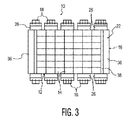
図1から図5を参照すると、本発明による超音波トランスデューサ用の超音波センサ組立体は一般的に10のように構成され、トランスデューサエレメント14のアレイ12、及びここではバッキングブロック16と呼ばれる相互接続構造を含む。この相互接続構造は、前記アレイ12と、超音波撮像システム(図示せず)の画像処理及び表示ユニットにつながる柔軟な相互接続ケーブル18との間に挿入され、これらを相互接続する。バッキングブロック16は、マイクロビーム形成部20及び再分配相互接続装置又は再分配インターポーザ22を含む。センサ組立体10は、超音波撮像システムに対し移動可能である共通するトランスデューサハウジング内に配される。
Referring to FIGS. 1-5, an ultrasonic sensor assembly for an ultrasonic transducer according to the present invention is generally configured as 10 and includes an
マイクロビーム形成部20は、相互接続構造、すなわち接触パッド、接着パッド又は他の形式の導電性接続部材28のパターンを規定する複数のベース部品24を含み、このベース部品は、一側面上において再分布インターポーザ22及び複数の補助電子部品がそれに電気接続されることを可能にする。この相互接続構造は、前記接着パッド28とベース部品24の電子部品との間に配線も含む。ベース部品24は、HVIC(high voltage integrated circuit)、特にASIC(application specified integrated circuit)でもよく、補助部品26はLVIC(low voltage integrated circuit)、特にASIC及び/又はFPGA(field programmable gate array)でもよい。
The
マイクロビーム形成部20により行われるビーム形成に必要な機能は、ベース部品24又は補助部品26の構造、及びどの形式の部品がその機能を最良に行うことできるかに依存して、これら部品の特定の機能に割り当てられる。ベース部品24としてHVICが使用され、補助部品26としてLVICが使用される実施例において、マイクロビーム形成部20の電子機能はこれにより、別々の高電圧部品及び低電圧部品において実施され、特に最適性能を提供する部品の形式で実施される。
The functions required for beamforming performed by the
一般的に、各ベース部品24は、トランスデューサエレメント14に送信ビームを発生させるために、トランスデューサエレメント14に送られる送信パルスを生成するドライバを含み、各補助部品26は、ベース部品24への入力の役割を果たす送信波形を発生させる回路、トランスデューサエレメント14からの反射パルスを受信し、これら反射パルスを遅延させるための時間遅延回路及び/又はビーム形成した信号を発生させるために、前記遅延した反射パルスの群を合計する加算回路を含んでいる。補助部品26により行われることが可能である他の機能は、位相収差補正、焦点制御、音速補正、マルチビーム処理、サブマイクロビーム形成、相互相関、データ処理及び完全なビーム形成を含む。ベース部品24はトランスデューサエレメント14から信号を受信する最初の電子部品であるため、これらベース部品24がトランスデューサエレメント14からの受信信号を増幅する受信プリアンプを含んでもよい。ベース部品24及び補助部品26の構成はこれにより、これら部品の特定用途に別々に依存している。
In general, each
例えばHVIC及びLVICの両方のような、異なる構成及び割り当てられた機能を持つマイクロビーム形成部20に異なる形式の電子部品が存在することは、マイクロビーム形成部の性能に関して妥協する問題に対し解決策を提供する。本発明によるマイクロビーム形成部20により行われるアナログ及びデジタル機能は分離され、各々がHVIC若しくはLVICの一方により最適に行われるか、又は例えばFPGA、カスタムアナログ若しくはデジタル処理エンジン、サブビーム形成部若しくはスーパービーム形成部、低ノイズアナログ回路、又はケーブル若しくは無線通信モジュールのような他の同等な電子部品により最適に行われる。電力消費、回路の複雑性及び送電の間におけるトレードオフは、従って有利に対処される。
The presence of different types of electronic components in the
再分配インターポーザ22は、ベース部品24の上面にある接着パッド28を、この再分配インターポーザ22の露出した上面及び下面内及びこれら面上にある導電材料を介して、トランスデューサエレメント14に相互接続するように構成される。トランスデューサエレメント14と再分配インターポーザ22との接続は、標準的なトランスデューサ組み立て工程(図1及び図2参照)を用いて、それらの間に導電材料30を形成することにより得られる。ベース部品の接着パッド28と再分配インターポーザ22との接続は、例えば銀−エポキシ浸漬法を用いて、それらの間に導電材料32を形成することにより得られる。ベース部分の接着パッド28及びトランスデューサエレメント14に接続するために、再分配インターポーザ22の両面に接着パッドを設けることが可能である。
The
マイクロビーム形成部20のベース部品24と前記アレイ12のトランスデューサエレメント14との相互接続に加え、前記アレイ12のフットプリントがベース部品24上にある接着パッド28のフットプリントと異なるように、前記マイクロビーム形成部20に関する空間制約をトランスデューサエレメント14のアレイ12の空間制約から切り離すことが再分配インターポーザ22の重要な目的である。説明される実施例において、再分配インターポーザ22は、一対の対向する縁又は側面34に関し、外側からベース部品24へ先細りとなり(図2参照)、他の対の対向する縁又は側面36に関し、ベース部品24から内側へ先細りとなる(図1参照)。これにより、一次元では、トランスデューサエレメント14が接続される再分配インターポーザ22の側面38は、ベース部品24が接続される再分配インターポーザ22の側面40よりも大きい一方、他の直交次元では、側面38は側面40よりも小さい(図1参照)。再分配インターポーザ22の側面34、36が先細りする程度は、例えば接着パッドのピッチのような様々な要因に基づいている。実際には、ベース部品24をフリップチップ接着するための接着パッドのピッチは、100ミクロンほどの密接さとすることが可能であるため、かなりの先細りが可能である。他方では、トランスデューサハウジングは通例、このハウジングの口径よりも仰角次元において僅かに大きいため、前記先細りにより提供される空間に加え、幾らかの余分な空間が利用可能となる。
In addition to the interconnection of the
再分配インターポーザ22は、ベース部品24とトランスデューサエレメント14とを絶縁するのにも効果的であり、これによりベース部品24とトランスデューサエレメント14との間における相互作用から生じる音響アーチファクトを減少させる。
The
トランスデューサアレイを様々な形状で使用するための再分配インターポーザ22の代替構造は、2005年1月11日出願の米国特許出願シリアル番号60/642,911(出願人整理番号PHUS050020US)に開示され、ここで参照することにより取り入れたこととする。例えば、湾曲したトランスデューサアレイが供給され、本出願に開示されるような直線の下面と対向する湾曲面とを持つ再分配インターポーザを使用してベース部品24に接続されることができる。
An alternative construction of the
説明される実施例には、ベース部品24として5個のHVIC、補助部品26として10個のLVICが存在し、各HVICは前記上面に形成される接着パッド26のアレイを持つ(図4参照)。再分配インターポーザ22は、接着パッドアレイ42の中央の相互接続区間44にある接着パッド28の第1の組に接続され、補助部品24である一対のLVICは、この中央の相互接続区間44より外側の側方区間46に配される接着パッドの第2の組に接続される。側方区間46において接着パッド28に接続されるLVICは従って、再分配インターポーザ22に沿って配され、この再分配インターポーザ22は中央の相互接続区間44において接着パッドと接続している。相互接続ケーブル18のフレックス回路は、側方区間46より外側の周辺区間48において接着パッド28の第3の組に接続される。各区間44、46、48は、各HVIC24が再分配インターポーザ22、一対のLVIC26及び一対の相互接続ケーブル18に接続されるように、複数のHVIC24からの接着パッド28を含む。しかしながら、LVIC26の数及びサイズに依存して、各HVIC24が、数個のエレメント、例えば再分配インターポーザ22、単一のLVIC26及び単一の相互接続ケーブル18と接続することが可能である。
In the described embodiment, there are 5 HVICs as
図5は、トランスデューサアレイ12を介して超音波パルスを送信させるための信号を受信する入/出力(I/O)区間、例えば増幅、遅延及び送信波形の生成のような、1つ以上の信号処理機能を行うLVIC又は同等の補助部品を有する初期信号処理区間52、高電圧送信及び前置増幅のような1つ以上の信号処理機能を行う(及び再分配インターポーザ22が接続される)HVIC又は同等のベース部品を有する一次信号処理区間54、受信信号に関する1つ以上の信号処理機能を行うLVIC又は同等の補助部品を有する最終信号処理区間56、及び処理された受信信号を出力する入/出力(I/O)区間58を有するマイクロビーム形成部20の一般的な構造を示す。これら様々な区間と部品との間にある相互接続は、各HVICの相互接続構造、例えばHVICの一方の側面上に形成される接着パッド及びこれら接着パッドとHIVCの部品との間の配線により供給される。
FIG. 5 illustrates one or more signals such as input / output (I / O) sections that receive signals for transmitting ultrasonic pulses through the
図1から図3に示されるように、ベース部品24をシステムの処理ユニットに接続する相互接続ケーブル18が存在している。相互接続ケーブルを設ける代わりに、無線周波数(RF)変調機/送信機を補助部品又は補助部品の一部として設けることが可能であり、この場合、データは補助部品とシステムの処理ユニットとの間を無線で送信されることが可能である。これにより、マイクロビーム形成部20とシステムの処理ユニットとの間でのデータの送信は、有線又は無線方式で行われる。RF変調機/送信機は従って、信号処理区画52、56の一部、又代わりにI/O区画50、58の一部とすることができる。
As shown in FIGS. 1-3, there is an
本発明によるバッキングブロック、又はこのバッキングブロック及び本発明によるトランスデューサエレメントのアレイを含む超音波センサ組立体の一般的な実施例は、1つのHVICのような単一のベース部品及び1つLVICのような単一の補助部品であるほど小さく、並びにHVICの上面において接着パッドに接着されている再分配インターポーザであるほど小さい。2、3個のトランスデューサエレメントだけを備える小さなアレイが適当であってもよい。このアレイのサイズが増大するにつれて、HVICの数、LVICの数及び再分配インターポーザのサイズが増大する。 A typical embodiment of an ultrasonic sensor assembly comprising a backing block according to the invention or an array of transducer elements according to the backing block and the invention is a single base part such as one HVIC and one LVIC. The smaller the smaller auxiliary component, the smaller the redistribution interposer that is bonded to the adhesive pad on the top surface of the HVIC. A small array with only a few transducer elements may be appropriate. As the size of this array increases, the number of HVICs, the number of LVICs, and the size of the redistribution interposer increase.
それらの構造に依存する別々の機能を行う別個の電子部品、例えばHVIC及びLVICの両方を含むマイクロビーム形成部20と、フリップチップ接着を使用して、このマイクロビーム形成部に対し相互接続するとき、ピッチ整合要件を不要にする再分配インターポーザ22とを組み合わせることに幾つかの利点が存在している。利点は、利用可能な標準的なセルライブラリを用いた高度な機能を持つ低電圧、低電力、高密度のASIC技術を用いたデジタル回路を製造する能力、より大きな形状であるが、デジタル機能が無いために利用可能な空間に容易に嵌合することができる高電圧のASICに高電圧アナログ回路を制限する能力、並びにデジタル区間とアナログ区間とを互いに全体的に仕切ることであり、これにより潜在的なノイズ及び干渉を減少させる仕切りを含んでいる。加えて、相互接続構造のサイズ及び重量は、フリップチップ相互接続構造と類似している一方、バッキング相互接続構造におけるコードをまさる改善を提供している。
When interconnecting to the microbeamformer using flip-chip bonding and a separate electronic component that performs different functions depending on their structure, eg, both HVIC and LVIC There are several advantages to combining with a
その上、ベース部品により規定される相互接続構造が標準化される場合、異なるアレイピッチを順応させるために、再分配インターポーザに変化を加えてASICの再利用を可能にする。すなわち、以下に記載されるような製造工程において、如何なる変更も必要とせずに新しい構成が利用可能となるので、LVICがアップグレードされたLVICと交換されることが考えられる。ベース部品24又はHVICは、マイクロビーム形成部20の一部として残っている一方、補助部品26又はLVICは、アップグレードしたマイクロビーム形成部20を構成するために交換される。
In addition, when the interconnect structure defined by the base components is standardized, the redistribution interposer is modified to allow ASIC reuse to accommodate different array pitches. That is, in a manufacturing process as described below, a new configuration can be used without requiring any changes, so it is conceivable that the LVIC is replaced with an upgraded LVIC. The
その上、異なる性能を持つ様々なLVICが同時に製造され、センサ組立体10に組み込むための顧客による選択を利用可能にする。これにより、同じベース部品24又はHVIC及び同じ再分配インターポーザ22を使用して、異なるマイクロビーム形成部20(並びに、これにより異なるバッキングブロック16及び異なるセンサ組立体10)は、HVICのベース部品24の上に実装される補助部品26又はLVICの性能を変更することにより製造される。各センサ組立体10の値段は、補助部品26又はLVICの性能に依存している。
In addition, various LVICs with different capabilities are manufactured simultaneously, making customer choices available for incorporation into the
他の利点は、線形増幅器から前記エレメントへのリード線の長さは短いので、駆動している相互接続キャパシタンスにおいて電力が殆ど浪費されないことである。さらに、高電圧のASIC技術は、デジタル形状に関係なく選択されることができるので、低電圧出力へつながる妥協は解消され、透過率及び画像品質が向上する。 Another advantage is that little power is wasted on the driving interconnect capacitance because the length of the lead from the linear amplifier to the element is short. In addition, high voltage ASIC technology can be selected regardless of the digital shape, so the compromise leading to low voltage output is eliminated, and transmission and image quality are improved.
トランスデューサエレメント14のアレイ12、バッキングブロック16及び相互接続ケーブル18を含む超音波センサ組立体10は、様々な異なる方法で製造されることが可能である。ある例示的な製造方法は、例えば標準的なトランスデューサ組み立て工程を用いて、再分配インターポーザ22の上面にある接着パッドに前記アレイ12のトランスデューサエレメント14を電気接続することである。ベース部品24上にある接着パッド(区間44における接着パッド)28は、例えば低温フリップチップ処理又は銀−エポキシ浸漬処理を介して、再分配インターポーザ22の下面にある接着パッドに電気接続され、この再分配インターポーザ22の下面にある接着パッドは、この再分配インターポーザ22内にある電気接続を介して、再分配インターポーザ22の上面にある接着パッドに電気接続されている。補助部品26は、例えばフリップチップ相互接続を用いて、ベース部品24の側方区間上にある接着パッド(区間46における接着パッド)28に電気接続されている。前記相互接続ケーブル18は、ベース部品24の周辺区間上にある追加の接着パッド(区間48における接着パッド)28に電気接続されている。
The
再分配インターポーザ22は、バッキング技術においてコードを用いて好ましくは形成されるので、センサ組立体10の構造はこれにより、フリップチップ相互接続技術、及びバッキング技術における前記コードの両方を用いることを含む。両方の組み立て技術を使用することは、各個別の技術の欠点を減少又は削除するハイブリッド設計となる。設計に対するより好ましい兼ね合いはこれにより可能な限り与えられる。
Since the
超音波センサ組立体が組み立てられる順序、すなわち前記部品間の電気接続が行われる順序は変更可能である。好ましい電気接続の順序は、最初にトランスデューサエレメント14を再分配インターポーザ22に接続し、次いで補助部品26、例えばLVICをベース部品24、例えばHVICに接続し、次いで相互接続ケーブル18をHVIC24に接続し、最後にHVIC24を再分配インターポーザ22に接続する。HVIC及びLVICの組立体は、HVIC24を再分配インターポーザ22に接続する前に、検査されることも可能である。最後に一度センサ組立体10が完成したら、この組立体は検査される。
The order in which the ultrasonic sensor assemblies are assembled, i.e. the order in which the electrical connections between the parts are made, can be changed. The preferred electrical connection sequence is to first connect the
その上、センサ組立体10の組み立て中、前記部品の様々な検査が行われてもよい。例えば、トランスデューサ14と再分配インターポーザ22との間の接続は、これら部品が一緒に接続された後に検査されてもよい。
In addition, various inspections of the parts may be performed during assembly of the
センサ組立体10は、超音波トランスデューサを含む超音波撮像システム、例えば医用超音波撮像システムの如何なる形式でも使用されることが可能である。トランスデューサアレイへの相互接続を用いた低電圧電子機器及び高電圧電子機器の密な相互接続が必要とされるこれら応用にとって特に有用である。
The
説明される本発明の実施例が添付する図面を参照して説明されたとしても、本発明がこれらの厳密な実施例に制限されず、様々な他の変更及び修正が本発明の範囲及び意図から外れることなく、当業者により行われるかもしれないことを理解している。 Although the embodiments of the invention described are described with reference to the accompanying drawings, the invention is not limited to these exact embodiments, and various other changes and modifications may be within the scope and intent of the invention. It is understood that this may be done by those skilled in the art without departing from the scope.
Claims (18)
ベース電子部品の第1の側面に相互接続構造のパターンを規定している少なくとも1つのベース電子部品、
第1の側面において、前記少なくとも1つのベース部品の前記第1の側面にある前記相互接続構造に電気結合され、対向する第2の側面において、前記トランスデューサエレメントの前記アレイに電気結合されるように適合した再分配インターポーザ、及び
前記ベース部品の前記第1の側面において、前記相互接続構造を介して前記少なくとも1つのベース部品に電気接続され、前記再分配インターポーザに沿って配される少なくとも1つの補助電子部品
を有するバッキングブロック。 In a backing block for interconnecting an array of transducer elements in an ultrasonic transducer and a processing unit of an ultrasonic imaging system,
At least one base electronic component defining a pattern of interconnect structure on a first side of the base electronic component;
In a first aspect, electrically coupled to the interconnect structure on the first side of the at least one base component and electrically coupled to the array of transducer elements on an opposing second side. An adapted redistribution interposer and, on the first side of the base part, at least one auxiliary electrically connected to the at least one base part via the interconnect structure and arranged along the redistribution interposer Backing block with electronic components.
パルスを送信及び受信するためであり、前記再分配インターポーザの前記第2の側面に接続されるトランスデューサエレメントのアレイ、及び
前記少なくとも1つのベース部品に接続される少なくとも1つの相互接続ケーブル
を有するセンサ組立体。 The backing block according to claim 1,
Sensor set for transmitting and receiving pulses and having an array of transducer elements connected to the second side of the redistribution interposer and at least one interconnect cable connected to the at least one base component Solid.
再分配インターポーザの一方の側面に前記アレイを電気接続するステップ、
前記再分配インターポーザの対向する側面を、相互接続構造のパターンを規定する少なくとも1つのベース部品に電気接続するステップ、
前記再分配インターポーザ及び前記少なくとも1つの補助部品が前記少なくとも1つのベース部品の共通側面に配され、前記少なくとも1つの補助部品が前記少なくとも1つのベース部品とは異なる機能を持つように、少なくとも1つの補助部品を前記再分配インターポーザに沿って前記少なくとも1つのベース部品に電気接続されるステップ、
前記少なくとも1つのベース部品を有線又は無線方式で前記超音波プローブに結合するステップ、及び
前記少なくとも1つのベース部品及び前記少なくとも1つの補助部品を別々に構成し、前記構成に基づいて別々の機能を前記少なくとも1つのベース部品及び前記少なくとも1つの補助部品に割り当てるステップ
を有する方法。 In a method of interconnecting an array of transducer elements and an ultrasonic probe,
Electrically connecting the array to one side of the redistribution interposer;
Electrically connecting opposite sides of the redistribution interposer to at least one base component defining a pattern of interconnect structures;
At least one such that the redistribution interposer and the at least one auxiliary part are arranged on a common side of the at least one base part, the at least one auxiliary part having a different function than the at least one base part Electrically connecting an auxiliary component to the at least one base component along the redistribution interposer;
Coupling the at least one base component to the ultrasound probe in a wired or wireless manner; and configuring the at least one base component and the at least one auxiliary component separately, and providing different functions based on the configuration. Assigning to the at least one base part and the at least one auxiliary part.
前記少なくとも1つのベース部品の内側において、前記再分配インターポーザを接着パッドの第1の組に接続するステップ、
前記少なくとも1つの補助部品を、前記接着パッドの第1の組の周りにある接着パッドの第2の組に接続するステップ、及び
少なくとも1つの相互接続ケーブルを、前記接着パッドの第2の組の周りにある接着パッドの第3の組に接続するステップ
を有する請求項12に記載の方法。 Connecting the redistribution interposer to a first set of adhesive pads inside the at least one base component;
Connecting the at least one auxiliary component to a second set of bond pads around the first set of bond pads; and at least one interconnect cable to the second set of bond pads. 13. The method of claim 12, comprising connecting to a third set of surrounding adhesive pads.
Applications Claiming Priority (2)
| Application Number | Priority Date | Filing Date | Title |
|---|---|---|---|
| US68800705P | 2005-06-07 | 2005-06-07 | |
| PCT/IB2006/051785 WO2006131875A2 (en) | 2005-06-07 | 2006-06-05 | Multicomponent backing block for ultrasound sensor assemblies |
Publications (1)
| Publication Number | Publication Date |
|---|---|
| JP2008545501A true JP2008545501A (en) | 2008-12-18 |
Family
ID=37216126
Family Applications (1)
| Application Number | Title | Priority Date | Filing Date |
|---|---|---|---|
| JP2008515354A Pending JP2008545501A (en) | 2005-06-07 | 2006-06-05 | Backing block for ultrasonic sensor assembly |
Country Status (6)
| Country | Link |
|---|---|
| US (1) | US20080229835A1 (en) |
| EP (1) | EP1890825A2 (en) |
| JP (1) | JP2008545501A (en) |
| KR (1) | KR20080021635A (en) |
| CN (1) | CN101193711B (en) |
| WO (1) | WO2006131875A2 (en) |
Cited By (2)
| Publication number | Priority date | Publication date | Assignee | Title |
|---|---|---|---|---|
| JP2007130385A (en) * | 2005-11-14 | 2007-05-31 | Aloka Co Ltd | Ultrasonic probe and backing for use in the same |
| JP2015033571A (en) * | 2013-07-10 | 2015-02-19 | コニカミノルタ株式会社 | Phasing adder and ultrasonic probe |
Families Citing this family (12)
| Publication number | Priority date | Publication date | Assignee | Title |
|---|---|---|---|---|
| JP4969456B2 (en) * | 2005-01-11 | 2012-07-04 | コーニンクレッカ フィリップス エレクトロニクス エヌ ヴィ | Redistribution interconnect for microbeamformers and medical ultrasound systems |
| US7892176B2 (en) | 2007-05-02 | 2011-02-22 | General Electric Company | Monitoring or imaging system with interconnect structure for large area sensor array |
| EP2669019A1 (en) * | 2009-03-26 | 2013-12-04 | Norwegian University of Science and Technology (NTNU) | An acoustic damping structure for use in an ultrasound transducer |
| RU2533336C2 (en) * | 2009-09-03 | 2014-11-20 | Конинклейке Филипс Электроникс Н.В. | Ultrasonic sensor with wide field of view, and manufacturing method of such ultrasonic sensor |
| US8345508B2 (en) * | 2009-09-20 | 2013-01-01 | General Electric Company | Large area modular sensor array assembly and method for making the same |
| US9649091B2 (en) | 2011-01-07 | 2017-05-16 | General Electric Company | Wireless ultrasound imaging system and method for wireless communication in an ultrasound imaging system |
| ES2938849T3 (en) | 2014-07-11 | 2023-04-17 | Microtech Medical Technologies Ltd | multi-cell transducer |
| WO2016083985A1 (en) | 2014-11-25 | 2016-06-02 | Koninklijke Philips N.V. | A multi-sensor ultrasound probe and related methods |
| US10001459B2 (en) | 2015-02-27 | 2018-06-19 | General Electric Company | System and method for phased array edge card |
| US9751108B2 (en) * | 2015-07-31 | 2017-09-05 | Texas Instruments Incorporated | Extended range ultrasound transducer |
| US20180317888A1 (en) | 2015-11-24 | 2018-11-08 | Koninklijke Philips N.V. | Ultrasound systems with microbeamformers for different transducer arrays |
| CN111698950A (en) * | 2018-02-08 | 2020-09-22 | 皇家飞利浦有限公司 | Wireless operation for transesophageal echocardiography |
Citations (9)
| Publication number | Priority date | Publication date | Assignee | Title |
|---|---|---|---|---|
| US6100626A (en) * | 1994-11-23 | 2000-08-08 | General Electric Company | System for connecting a transducer array to a coaxial cable in an ultrasound probe |
| JP2002345094A (en) * | 2001-05-22 | 2002-11-29 | Aloka Co Ltd | Backing for ultrasonic wave probe and its manufacturing method |
| US20030122206A1 (en) * | 2001-11-09 | 2003-07-03 | Amal Bhattarai | Multi-chip module integrating MEMS mirror array with electronics |
| US20030204141A1 (en) * | 2002-04-30 | 2003-10-30 | Siemens Medical Solutions Usa, Inc. | Ultrasound drug delivery enhancement and imaging systems and methods |
| JP2004514340A (en) * | 2000-11-15 | 2004-05-13 | コーニンクレッカ フィリップス エレクトロニクス エヌ ヴィ | Multidimensional ultrasonic transducer array |
| JP2004282072A (en) * | 2003-03-14 | 2004-10-07 | General Electric Co <Ge> | Interposer, interposer package, and device assembly employing the same |
| WO2004096696A1 (en) * | 2003-04-25 | 2004-11-11 | Cavendish Kinetics Ltd | Method of manufacturing a micro-mechanical element |
| JP2004363746A (en) * | 2003-06-03 | 2004-12-24 | Fuji Photo Film Co Ltd | Ultrasonic probe and its manufacturing method |
| JP2005507581A (en) * | 2001-07-31 | 2005-03-17 | コーニンクレッカ フィリップス エレクトロニクス エヌ ヴィ | System for mounting acoustic elements to integrated circuits |
Family Cites Families (7)
| Publication number | Priority date | Publication date | Assignee | Title |
|---|---|---|---|---|
| US5460180A (en) * | 1994-09-30 | 1995-10-24 | Siemens Medical Systems, Inc. | Connection arrangement and method of operation of a 2D array for phase aberration correction |
| US6541896B1 (en) * | 1997-12-29 | 2003-04-01 | General Electric Company | Method for manufacturing combined acoustic backing and interconnect module for ultrasonic array |
| US6380766B2 (en) * | 1999-03-19 | 2002-04-30 | Bernard J Savord | Integrated circuitry for use with transducer elements in an imaging system |
| CN2384576Y (en) * | 1999-07-07 | 2000-06-28 | 上海麦迪逊医疗器械有限公司 | Short axle direction composite focusing convex transducer |
| US6589180B2 (en) * | 2001-06-20 | 2003-07-08 | Bae Systems Information And Electronic Systems Integration, Inc | Acoustical array with multilayer substrate integrated circuits |
| US6871049B2 (en) * | 2002-03-21 | 2005-03-22 | Cognio, Inc. | Improving the efficiency of power amplifiers in devices using transmit beamforming |
| US6784600B2 (en) * | 2002-05-01 | 2004-08-31 | Koninklijke Philips Electronics N.V. | Ultrasonic membrane transducer for an ultrasonic diagnostic probe |
-
2006
- 2006-06-05 KR KR1020077028297A patent/KR20080021635A/en not_active Application Discontinuation
- 2006-06-05 WO PCT/IB2006/051785 patent/WO2006131875A2/en active Application Filing
- 2006-06-05 US US11/916,762 patent/US20080229835A1/en not_active Abandoned
- 2006-06-05 EP EP06745061A patent/EP1890825A2/en not_active Withdrawn
- 2006-06-05 CN CN2006800203809A patent/CN101193711B/en not_active Expired - Fee Related
- 2006-06-05 JP JP2008515354A patent/JP2008545501A/en active Pending
Patent Citations (9)
| Publication number | Priority date | Publication date | Assignee | Title |
|---|---|---|---|---|
| US6100626A (en) * | 1994-11-23 | 2000-08-08 | General Electric Company | System for connecting a transducer array to a coaxial cable in an ultrasound probe |
| JP2004514340A (en) * | 2000-11-15 | 2004-05-13 | コーニンクレッカ フィリップス エレクトロニクス エヌ ヴィ | Multidimensional ultrasonic transducer array |
| JP2002345094A (en) * | 2001-05-22 | 2002-11-29 | Aloka Co Ltd | Backing for ultrasonic wave probe and its manufacturing method |
| JP2005507581A (en) * | 2001-07-31 | 2005-03-17 | コーニンクレッカ フィリップス エレクトロニクス エヌ ヴィ | System for mounting acoustic elements to integrated circuits |
| US20030122206A1 (en) * | 2001-11-09 | 2003-07-03 | Amal Bhattarai | Multi-chip module integrating MEMS mirror array with electronics |
| US20030204141A1 (en) * | 2002-04-30 | 2003-10-30 | Siemens Medical Solutions Usa, Inc. | Ultrasound drug delivery enhancement and imaging systems and methods |
| JP2004282072A (en) * | 2003-03-14 | 2004-10-07 | General Electric Co <Ge> | Interposer, interposer package, and device assembly employing the same |
| WO2004096696A1 (en) * | 2003-04-25 | 2004-11-11 | Cavendish Kinetics Ltd | Method of manufacturing a micro-mechanical element |
| JP2004363746A (en) * | 2003-06-03 | 2004-12-24 | Fuji Photo Film Co Ltd | Ultrasonic probe and its manufacturing method |
Cited By (4)
| Publication number | Priority date | Publication date | Assignee | Title |
|---|---|---|---|---|
| JP2007130385A (en) * | 2005-11-14 | 2007-05-31 | Aloka Co Ltd | Ultrasonic probe and backing for use in the same |
| JP4532392B2 (en) * | 2005-11-14 | 2010-08-25 | アロカ株式会社 | Ultrasonic probe and backing used therefor |
| JP2015033571A (en) * | 2013-07-10 | 2015-02-19 | コニカミノルタ株式会社 | Phasing adder and ultrasonic probe |
| US10001460B2 (en) | 2013-07-10 | 2018-06-19 | Konica Minolta, Inc. | Phasing adder and ultrasound probe |
Also Published As
| Publication number | Publication date |
|---|---|
| EP1890825A2 (en) | 2008-02-27 |
| WO2006131875A3 (en) | 2007-03-29 |
| CN101193711B (en) | 2010-12-29 |
| US20080229835A1 (en) | 2008-09-25 |
| WO2006131875A2 (en) | 2006-12-14 |
| CN101193711A (en) | 2008-06-04 |
| KR20080021635A (en) | 2008-03-07 |
Similar Documents
| Publication | Publication Date | Title |
|---|---|---|
| JP2008545501A (en) | Backing block for ultrasonic sensor assembly | |
| US7795784B2 (en) | Redistribution interconnect for microbeamforming(s) and a medical ultrasound system | |
| US20220079559A1 (en) | Modular piezoelectric sensor array with co-integrated electronics and beamforming channels | |
| US6551248B2 (en) | System for attaching an acoustic element to an integrated circuit | |
| US6758094B2 (en) | Ultrasonic transducer wafer having variable acoustic impedance | |
| US20080294050A1 (en) | Ultrasonic Imaging Apparatus | |
| WO2003001571A2 (en) | Acoustical array with multilayer substrate integrated circuits | |
| CN112118791A (en) | Integrated ultrasonic transducer | |
| JP2008079909A (en) | Ultrasonic probe and ultrasonic imaging apparatus | |
| JP6759209B2 (en) | Compact ultrasonic transducer with direct coaxial mounting | |
| EP3069391B1 (en) | Robust ultrasound transducer probes having protected integrated circuit interconnects | |
| JP6761861B2 (en) | Extended Range Ultra Sound Transducer | |
| US20210016320A1 (en) | Ultrasound Transducer Array Interconnect | |
| KR20160066483A (en) | Ultrasound probe and manufacturing method for the same | |
| EP3432024B1 (en) | Bonding interposer and integrated circuit chip, and ultrasound probe using the same | |
| Savoia et al. | Integration of two-dimensional MEMS ultrasonic transducer arrays with front-end electronics for medical ultrasound imaging | |
| US11957513B2 (en) | Non-rectangular transducer arrays and associated devices, systems, and methods | |
| CN112638548A (en) | Non-rectangular transducer arrays and associated devices, systems, and methods | |
| KR20180068586A (en) | Probe for ultrasonic diagnostic apparatus |
Legal Events
| Date | Code | Title | Description |
|---|---|---|---|
| A621 | Written request for application examination |
Free format text: JAPANESE INTERMEDIATE CODE: A621 Effective date: 20090604 |
|
| A131 | Notification of reasons for refusal |
Free format text: JAPANESE INTERMEDIATE CODE: A131 Effective date: 20110616 |
|
| A02 | Decision of refusal |
Free format text: JAPANESE INTERMEDIATE CODE: A02 Effective date: 20120105 |