JP2008542904A - Memory controller and method for coupling network and memory - Google Patents
Memory controller and method for coupling network and memory Download PDFInfo
- Publication number
- JP2008542904A JP2008542904A JP2008514294A JP2008514294A JP2008542904A JP 2008542904 A JP2008542904 A JP 2008542904A JP 2008514294 A JP2008514294 A JP 2008514294A JP 2008514294 A JP2008514294 A JP 2008514294A JP 2008542904 A JP2008542904 A JP 2008542904A
- Authority
- JP
- Japan
- Prior art keywords
- buffer
- memory
- data
- network interface
- network
- Prior art date
- Legal status (The legal status is an assumption and is not a legal conclusion. Google has not performed a legal analysis and makes no representation as to the accuracy of the status listed.)
- Withdrawn
Links
Images


Classifications
-
- G—PHYSICS
- G06—COMPUTING; CALCULATING OR COUNTING
- G06F—ELECTRIC DIGITAL DATA PROCESSING
- G06F13/00—Interconnection of, or transfer of information or other signals between, memories, input/output devices or central processing units
- G06F13/14—Handling requests for interconnection or transfer
- G06F13/16—Handling requests for interconnection or transfer for access to memory bus
- G06F13/1668—Details of memory controller
- G06F13/1673—Details of memory controller using buffers
Landscapes
- Engineering & Computer Science (AREA)
- Theoretical Computer Science (AREA)
- Physics & Mathematics (AREA)
- General Engineering & Computer Science (AREA)
- General Physics & Mathematics (AREA)
- Data Exchanges In Wide-Area Networks (AREA)
- Bus Control (AREA)
- Communication Control (AREA)
Abstract
Description
本発明は、メモリコントローラ及びネットワークとメモリとを結合する方法に関する。 The present invention relates to a memory controller and a method for combining a network and a memory.
高度モバイル携帯機器の複雑度が増している。益々厳しくなるこのような機器のアプリケーション、複雑度、フレキシビリティ及びプログラマビリティ要件はデコーダ内部のデータ交換を増大している。このようなアプリケーションを実施するデバイスは多くの場合いくつかの機能ブロック又は処理ブロック(ここではサブシステムという)からなる。これらのサブシステムは代表的には個別のICとして実現され、各ICはローカルプロセッサ、バス及びメモリなどからなる異なる内部アーキテクチャを有する。また、種々のサブシステムは一つのICに集積することもできる。システムレベルでは、これらのサブシステムはトップレベルのインターコネクトを介して互いに通信し、所定のサービスを多くの場合リアルタイムサポートで提供する。携帯電話アーキテクチャ内のサブシステムの例としては、特にベースバンドプロセッサ、ディスプレイ、メディアプロセッサ又は記憶素子がある。マルチメディアアプリケーションをサポートするために、これらのサブシステムはデータの大部分をストリーム形式で交換する。データストリーミングの一例として、メディアプロセッサによるMP3符号化オーディオファイルの読出し及び復号ストリームのスピーカへの送出がある。このような通信は、しばしばKahnプロセスネットワークと呼ばれている、FIFOバッファを経て接続されるプロセスのグラフとして記述できる。Kahnプロセスネットワークは、E.A. de Kochet al. ”YAPI: Application modeling for signal processing systems”,In Proc. Of the 37th Design Automation Conference, Los Angels, CA, June 2000, pp.402-405,IEEE 2000、に記載されているように、システムアーキテクチャにマップすることができる。このようなアーキテクチャでは、プロセスがサブシステムに、FIFOがメモリにマップされ、通信がシステムレベルインターコネクトにマップされる。 The complexity of advanced mobile mobile devices is increasing. The increasingly demanding application, complexity, flexibility and programmability requirements of such devices increase the data exchange within the decoder. Devices that implement such applications often consist of several functional blocks or processing blocks (herein referred to as subsystems). These subsystems are typically implemented as individual ICs, each IC having a different internal architecture consisting of a local processor, bus, memory, and the like. Various subsystems can also be integrated in one IC. At the system level, these subsystems communicate with each other via top level interconnects and provide predetermined services, often with real-time support. Examples of subsystems within a mobile phone architecture are in particular baseband processors, displays, media processors or storage elements. In order to support multimedia applications, these subsystems exchange most of the data in a stream format. An example of data streaming is reading a MP3 encoded audio file by a media processor and sending a decoded stream to a speaker. Such communication can be described as a graph of processes connected via a FIFO buffer, often referred to as a Kahn process network. Kahn process network, EA de Kochet al.. " YAPI: Application modeling for signal processing systems", In Proc Of the 37 th Design Automation Conference, Los Angels, CA, June 2000, pp.402-405, IEEE 2000, to It can be mapped to a system architecture as described. In such an architecture, processes are mapped to subsystems, FIFOs are mapped to memory, and communications are mapped to system level interconnects.
バッファリングは関連するプロセス間のデータストリーミングの適切なサポートに不可欠である。ストリーミングにFIFOバッファを使用することは極めて当然のことであり、これはストリーミングアプリケーションの(有界)Kahnプロセスネットワークモデルに従う。同時に実行し得るマルチメディアアプリケーションの数が増加すると、プロセスの数、リアルタイムストリームの数並びに関連するFIFOの数が相当増加ずる。 Buffering is essential for proper support of data streaming between related processes. It is quite natural to use a FIFO buffer for streaming, which follows the (bounded) Kahn process network model for streaming applications. As the number of multimedia applications that can run simultaneously increases, the number of processes, the number of real-time streams, and the number of associated FIFOs increase considerably.
多くのシステムオンチップ(SoC)及びマイクロプロセッサシステムでは、データのバッファリングにバックグラウンドメモリ(DRAM)が使用される。データをストリーミング方式で通信し、メモリにストリームとしてバッファするとき、プリフェッチバッファリングを使用できる。これは、SDRAMからのデータを前もって読み出し、特別の(プリフェッチ)バッファに保持することを意味する。リード要求が到来すると、この要求は、さもなければバックグラウンドメモリ(DRAM)により導入されるレイテンシなしで、(通常オンチップSRAMに実装される)ローカルプリフェッチバッファからサービスされる。これはプロセッサに対するランダムデータのキャッシュ技術に類似する。ストリーミングの場合には、キャッシュに使用されるランダムアドレスではなくデータの連続(又は予測可能)アドレス指定がプリフェッチバッファに使用される。 In many system-on-chip (SoC) and microprocessor systems, background memory (DRAM) is used for buffering data. Prefetch buffering can be used when data is communicated in a streaming fashion and buffered as a stream in memory. This means that data from the SDRAM is read in advance and held in a special (prefetch) buffer. When a read request arrives, this request is serviced from a local prefetch buffer (usually implemented in on-chip SRAM) without the latency otherwise introduced by background memory (DRAM). This is similar to random data caching techniques for processors. In the case of streaming, continuous (or predictable) addressing of data is used for the prefetch buffer rather than the random address used for the cache.
他方、DRAM技術のために、DRAMへのアクセス(リード又はライト)はバースト単位に行う方がよい。単一ワードがDRAMメモリからアクセスされるとき、ACTIVEコマンドの発行後にDRAMのデータアレイからセンス増幅器へのメモリページのプリフェッチを実行するためにオーバヘッドが必要とされる。データがセンス増幅器へ転送されたとき、READコマンド後にセンス増幅器から活性化されたデータを読み出すために、データアドレスをデコーディングしデータを出力バッファへ転送するための初期時間が必要とされる。このようなオーバヘッドはDRAMメモリからその仕様に基づいて容易に計算できる。代表的には、このようなオーバヘッドは、数クロックサイクル(Tactive_to_read + Tread_to_data = TRCD +TCAS =2+3 = 5クロックサイクル)程度である。 On the other hand, because of DRAM technology, it is better to access (read or write) DRAM in burst units. When a single word is accessed from DRAM memory, overhead is required to perform prefetching of memory pages from the DRAM data array to the sense amplifier after issuing an ACTIVE command. When data is transferred to the sense amplifier, an initial time is required to decode the data address and transfer the data to the output buffer in order to read the activated data from the sense amplifier after the READ command. Such overhead can be easily calculated from DRAM memory based on its specifications. Typically, such overhead is about several clock cycles (T active_to_read + T read_to_data = T RCD + T CAS = 2 + 3 = 5 clock cycles).
DRAMメモリへのバーストアクセスを可能にするために、多数の単一データアクセスを所定のバーストサイズのバーストに集めるライトバックバッファが実現されている。初期プロセシングが最初のDRAMアクセスに対して実行されると、メモリの次のサイクル毎にアクセスされる次のデータワードが、(例えばバーストポリシーに基づいて)その前のデータワードに関連するアドレスで、即ち1つのストリーミングプロセスで、格納又は取り出され、所定数のアクセス(例えば2/4/8フルページ)に対して何の追加の遅延も生じない(1サイクル以内)。従って、アドレスがアクセス毎に単調に増加又は減少する(例えば連続アドレス)際のメモリへのストリーミングアクセスに対して、バーストアクセスは単位アクセスデータあたり最低の電力消費で最大のスループットという最良のパフォーマンスをもたらす。DRAMメモリの原理に関するもっと詳しい情報については、例えばマイクロンの128ビットDDRAMの使用を参照されたい。例えば、
(http://download.micron.com/pdf/datasheets/dam/ddr/128MbDDRx4x8x16.pdf)を参照されたい。
In order to allow burst access to DRAM memory, a write-back buffer has been implemented that collects multiple single data accesses into bursts of a predetermined burst size. When initial processing is performed for the first DRAM access, the next data word accessed in each next cycle of memory is the address associated with the previous data word (eg, based on burst policy), That is, in one streaming process, it is stored or retrieved and there is no additional delay (within 1 cycle) for a given number of accesses (eg 2/4/8 full pages). Thus, for streaming access to memory when the address monotonically increases or decreases with each access (eg, continuous address), burst access provides the best performance with the lowest power consumption per unit access data and maximum throughput. . See, for example, Micron's use of 128-bit DDRAM for more information on the principles of DRAM memory. For example,
Please refer to (http://download.micron.com/pdf/datasheets/dam/ddr/128MbDDRx4x8x16.pdf).
このような機能をDRAMメモリ用のメモリコントローラに実施する場合、内部バッファが存在しなければならない。メモリコントローラの内部バッファはデータキャッシュ、プリフェッチ及びライトバックバッファ、ストリーミング及びアービトレーションのためにも使用される。 When implementing such a function in a memory controller for DRAM memory, an internal buffer must be present. The internal buffer of the memory controller is also used for data cache, prefetch and write back buffers, streaming and arbitration.
DRAMメモリは頻繁にネットワーク又はバスを介してアクセスされるため、DRAMメモリのメモリコントローラをオンチップ/オフチップネットワークに結合でき、これはある種のフロー制御を実施できる。フロー制御は、一般にネットワーク内の各ネットワークノードでデータをバッファリングすることにより実施され、このバッファリングは、次のノードからアクノレッジが受信され、ネットワークハイアラーキネットワーク内の受信ノードのバッファが受信ノードへ転送されるデータパッケージを格納するのに使用できる十分なスペースを有することが確認されるまで行われる。このようなフロー制御メカニズムの利点は、バッファアンダーフロー/オーバフローが防止されるので、信頼できる転送が得られる点にある。 Since DRAM memory is frequently accessed over a network or bus, the memory controller of the DRAM memory can be coupled to an on-chip / off-chip network, which can implement some kind of flow control. Flow control is typically performed by buffering data at each network node in the network, which receives an acknowledgment from the next node and forwards the receiving node's buffer in the network hierarchy network to the receiving node. This is done until it is determined that there is enough space available to store the data package being processed. The advantage of such a flow control mechanism is that reliable transfer is obtained because buffer underflow / overflow is prevented.
図4は、送信ノード(ソースデバイスSD)及び受信ノード(宛先デバイスDD)のブロック図の一例を示す。ソースデバイスSDは、トランザクションペンディングバッファTPBと、送信ユニットTUと、受信ユニットRUと、受信フロー制御パケットユニットRFCPと、リミットクレジットレジスタCLRと、消費クレジットレジスタCCRと、フロー制御ユニットCUとを具える。トランザクションペンディングバッファTPBは任意のペンディングトランザクションをバッファするために使用される。送信ユニットTUはデータパケットを宛先デバイスDDに送信するために使用される。受信ユニットRUは宛先デバイスDDからのデータを受信するために使用される。受信フロー制御パケットユニットRFCPは宛先デバイスDDからの任意のフロー制御パケットを取り出すために使用される。宛先デバイスDDからのフロー制御パケットの取り出しに応じて、リミットクレジットCLがリミットクレジットレジスタCLRに格納される。消費クレジットレジスタCCRは消費されたクレジットCCを格納するために使用される。制御ユニットCUはリミットクレジットCLと消費クレジットとを比較するために使用される。リミットクレジットCLと消費クレジットとの差がトランザクションペンディングバッファにペンディング中のトランザクションのデータサイズより大きい場合、トランザクションを送ることができ、そうでなければ宛先デバイスDDから更なるクレジットを待つ。 FIG. 4 shows an example of a block diagram of a transmission node (source device SD) and a reception node (destination device DD). The source device SD includes a transaction pending buffer TPB, a transmission unit TU, a reception unit RU, a reception flow control packet unit RFCP, a limit credit register CLR, a consumption credit register CCR, and a flow control unit CU. Transaction pending buffer TPB is used to buffer any pending transactions. The transmission unit TU is used for transmitting data packets to the destination device DD. The receiving unit RU is used for receiving data from the destination device DD. The received flow control packet unit RFCP is used to retrieve any flow control packet from the destination device DD. In response to the extraction of the flow control packet from the destination device DD, the limit credit CL is stored in the limit credit register CLR. The consumption credit register CCR is used to store the consumed credit CC. The control unit CU is used to compare the limit credit CL with the consumption credit. If the difference between the limit credit CL and the consumed credit is larger than the data size of the transaction pending in the transaction pending buffer, the transaction can be sent, otherwise it waits for further credit from the destination device DD.
宛先デバイスDDは、受信ユニットRUと、送信ユニットTUと、送信フロー制御パケットユニットTFCPと、使用可能クレジットレジスタCARと、フロー制御バッファFCBとを具える。ソースデバイスSDからのトランザクションが受信ユニットRUにより受信される場合、このようなトランザクションはフロー制御バッファFCBに格納される。このトランザクションがフロー制御バッファFCBを出ると同時に、使用可能クレジットレジスタCARが増加される。使用可能クレジットレジスタCAR内の使用可能クレジットCAに従って、フロー制御パケットが送信フローパケットユニットTFCP内で用意され、送信ユニットTUに転送され、送信ユニットTUがフロー制御パケットをソースデバイスSDに送信する。 The destination device DD comprises a reception unit RU, a transmission unit TU, a transmission flow control packet unit TFCP, an available credit register CAR, and a flow control buffer FCB. When a transaction from the source device SD is received by the receiving unit RU, such a transaction is stored in the flow control buffer FCB. As soon as this transaction exits the flow control buffer FCB, the available credit register CAR is incremented. According to the available credit CA in the available credit register CAR, a flow control packet is prepared in the transmission flow packet unit TFCP, transferred to the transmission unit TU, and the transmission unit TU transmits the flow control packet to the source device SD.
フロー制御を実施するこのようなネットワークに関するもっと詳しい情報については、”PCI Express Base Specification, Revision 1.0”、 PCI-SIG(2002年7月)、Jasmin Aianovic and Hong Jiang著, “Multimedia and Quality of Service Support in PCI Express Architecture”、ホワイトペイパー、インテルコーポレーション(2002年9月12日)、Edward Solari and Brad Congdon著、“The Computer PCI Express Reference”、インテルプレス(2003年)を参照されたい。これらの3つの文献は参考のために援用されている。 For more information on such networks that implement flow control, see “PCI Express Base Specification, Revision 1.0”, PCI-SIG (July 2002), Jasmin Aianovic and Hong Jiang, “Multimedia and Quality of Service Support in PCI Express Architecture ”, White Paper, Intel Corporation (September 12, 2002), Edward Solari and Brad Congdon,“ The Computer PCI Express Reference ”, Intel Press (2003). These three documents are incorporated by reference.
図5は、フロー制御をメモリ制御で実施するネットワークとSDRANメモリとの組合せを具えるアーキテクチャのブロック図を示す。ネットワークNはいくつかのフロー制御バッファFCB並びにいくつかのトランザクションペンディングバッファTPBを具えることができる。ネットワークNはフロー制御ロジックのような他の素子(図5の明瞭化のために省略されている)も具えることができる。メモリコントローラMCは書込みバッファWBと読出しバッファRBを具えることができる。書込みバッファWB及び読出しバッファRBは、SDRAMメモリへのアクセスはバーストに基づいて行うのが好ましいために、必要とされる。データがネットワークNから発生すると、このデータは書込みバッファWBへ転送される。ネットワークフロー制御を満足するためにネットワーク内のフロー制御バッファにおいてバッファリングが実行される。書込みバッファWBにおいて、データは規定のデータバーストが得られるまで集められ、次いで単一のバースト内でメモリに書き込まれる。最初の数個の読出しトランザクション要求は書込みバッファWBにおいてメモリから転送されるべきデータのために集められ、次いでデータが単一バーストにてメモリから読出しバッファRBへ転送される。 FIG. 5 shows a block diagram of an architecture comprising a combination of a network that implements flow control with memory control and a SDRAN memory. The network N can comprise several flow control buffers FCB as well as several transaction pending buffers TPB. The network N can also include other elements such as flow control logic (omitted for clarity of FIG. 5). The memory controller MC can include a write buffer WB and a read buffer RB. The write buffer WB and read buffer RB are required because access to the SDRAM memory is preferably based on bursts. When data originates from the network N, this data is transferred to the write buffer WB. Buffering is performed in the flow control buffer in the network to satisfy the network flow control. In the write buffer WB, data is collected until a defined data burst is obtained and then written to memory within a single burst. The first few read transaction requests are collected for data to be transferred from memory in write buffer WB, and then the data is transferred from memory to read buffer RB in a single burst.
本発明の目的は、ネットワークとメモリとの間のフロー制御が改善された、ネットワークとメモリとを結合するメモリコントローラ並びにネットワークとメモリを結合する方法を提供することにある。 It is an object of the present invention to provide a memory controller for combining a network and a memory and a method for combining a network and a memory, with improved flow control between the network and the memory.
本発明の目的は、請求項1に係るメモリコントローラ及び請求項6に係るネットワークとメモリとの結合方法によって解決される。 The object of the present invention is solved by a memory controller according to claim 1 and a network and memory coupling method according to claim 6.
従って、本発明によればメモリをネットワークに結合するためのメモリコントローラが提供される。ネットワークは、ネットワークのフロー制御を実現するためにネットワークインターフェースバッファを有する少なくとも1つのネットワークインターフェースを具える。メモリコントローラは、ネットワークからのデータのバッファリングをメモリとバースト単位にデータ交換するように管理するバッファマネジメントユニットを具える。バッファマネジメントユニットは、更に、ネットワークインターフェースバッファをモニタして、データバーストをメモリに書き込むことができるような十分なデータがネットワークインターフェースバッファに存在するか、及び、メモリからのデータバーストをネットワークインターフェースバッファにバッファすることができるような十分なスペースがネットワークインターフェースバッファに使用可能であるかを決定する。バッファマネジメントユニットはメモリへのアクセスをネットワークイメージバッファ内のデータ及び/又は使用可能スペースの量に従って制御する。 Thus, according to the present invention, a memory controller for coupling a memory to a network is provided. The network includes at least one network interface having a network interface buffer to implement network flow control. The memory controller includes a buffer management unit that manages buffering of data from the network so as to exchange data in units of bursts with the memory. The buffer management unit further monitors the network interface buffer and there is sufficient data in the network interface buffer to write the data burst to the memory, and the data burst from the memory to the network interface buffer. Determine if enough space is available for the network interface buffer to be buffered. The buffer management unit controls access to the memory according to the amount of data and / or available space in the network image buffer.
ネットワークインターフェースバッファ(フロー制御バッファ及びトランザクションペンディングバッファ)を用いて実施される上述の如きメモリコントローラのバッファリングは、シリコン利用効率が向上するので有利である。PCI Expressインターフェースのフロー制御バッファとメモリコントローラ内のバーストバッファを別個に実現する場合には、大きなシリコン領域が必要とされ、これが避けられる。更に、不必要なデータコピーも避けられるため、必要とされるアクティビティ、従ってパワーが低くなる。単一バッファ(リード用の単一バッファ及びライト用の単一バッファ)は、それぞれに2つのバッファを使用する場合より遅延及びレイテンシが小さくなり有利である。ネットワークインターフェースにおけるフロー制御バッファは構造的に変更する必要はない。 Buffering of the memory controller as described above, implemented using network interface buffers (flow control buffer and transaction pending buffer) is advantageous because it improves silicon utilization efficiency. If the flow control buffer of the PCI Express interface and the burst buffer in the memory controller are implemented separately, a large silicon area is required, which is avoided. Furthermore, unnecessary data copying is avoided, so that less activity is required and thus less power. A single buffer (a single buffer for reading and a single buffer for writing) is advantageous in that the delay and latency are smaller than when two buffers are used for each. The flow control buffer in the network interface does not need to be structurally changed.
本発明の一つの態様では、ネットワークインターフェースは、PCI Expressネットワークの特性及びネットワークサービスをメモリコントローラで実現できるように、PCI Expressインターフェースとして実現される。 In one aspect of the present invention, the network interface is implemented as a PCI Express interface so that the characteristics of the PCI Express network and network services can be implemented by the memory controller.
本発明の一つの態様では、バッファマネジメントユニットは、ネットワークインターフェースバッファ内のスペースの量を格納する第1のレジスタと、ネットワークインターフェースバッファ内のデータの量を格納する第2のレジスタと、メモリへの及びからのアクセスを、前記スペースの量と前記データの量とバーストサイズとに基づいて制御する制御手段とを具える。 In one aspect of the invention, the buffer management unit includes a first register that stores the amount of space in the network interface buffer, a second register that stores the amount of data in the network interface buffer, and And control means for controlling access from and based on the amount of space, the amount of data and the burst size.
本発明の一つの態様では、バーストマネジメントユニットは、前記第1及び第2のレジスタを更新するために、データがネットワークインターフェースからネットワークへ転送されるとき、第1の情報を、データがネットワークインターフェースからメモリへ転送されるとき、第2の情報を受信する。 In one aspect of the invention, the burst management unit is configured to update the first information when the data is transferred from the network interface to the network in order to update the first and second registers. When transferred to the memory, the second information is received.
本発明の一つの態様では、ネットワークインターフェースバッファは各フロー制御仮想チャネル毎に設ける。フロー制御バッファは各仮想チャネル毎に個別に実現されるので、種々のストリームの弁別をコントローラで実施する必要はない。 In one aspect of the invention, a network interface buffer is provided for each flow control virtual channel. Since the flow control buffer is individually implemented for each virtual channel, it is not necessary to discriminate various streams by the controller.
本発明は、メモリをネットワークに結合する方法にも関するものであり、前記ネットワークはネットワークのフロー制御を実施するためにバッファを有する少なくとも一つのネットワークインターフェースを具える。バッファマネジメントユニットによって、ネットワークからのデータを前記メモリとバースト単位にデータ交換するように管理する。更に、前記ネットワークインターフェース内のバッファをモニタして、データバーストをメモリに書き込むことができるような十分なデータがネットワークインターフェースバッファに存在するか、及び、メモリからのデータバーストをネットワークインターフェースバッファにバッファすることができるような十分なスペースがネットワークインターフェースバッファに使用可能であるかを決定する。前記ネットワークインターフェースバッファ内の前記データの量及び/又は前記使用可能なスペースの量に従ってメモリへのアクセスを制御する。 The present invention also relates to a method for coupling memory to a network, the network comprising at least one network interface having a buffer for performing network flow control. The buffer management unit manages data exchanged with the memory in burst units. In addition, a buffer in the network interface is monitored to ensure that there is sufficient data in the network interface buffer to write the data burst to the memory and to buffer the data burst from the memory in the network interface buffer. To determine if enough space is available for the network interface buffer. Control access to memory according to the amount of data in the network interface buffer and / or the amount of available space.
本発明は、フロー制御を実施するために使用されるネットワークインターフェースバッファを、メモリコントローラのバーストバッファとして利用するという着想に基づく。このようなフロー制御バッファ及びトランザクションペンディングバッファの実現は従来の別個のバッファより大きいが、フロー制御バッファ及びトランザクションペンディングバッファはフロー制御バッファと(SDRAM)メモリ用のメモリコントローラ内の従来のバーストバッファとの和より小さい。 The present invention is based on the idea of using a network interface buffer used to implement flow control as a burst buffer of a memory controller. Although the implementation of such a flow control buffer and transaction pending buffer is larger than a conventional separate buffer, the flow control buffer and transaction pending buffer are a combination of a flow control buffer and a conventional burst buffer in a memory controller for (SDRAM) memory. Less than the sum.
他の特徴は従属請求項に特定されている。 Other features are specified in the dependent claims.
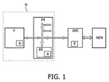
図1は、本発明に係るシステムオンチップの基本アーキテクチャのブロック図を示す。このシステムオンチップは、少なくとも1つの処理ユニットP(図1には1つの処理ユニットしか示されていない点に注意されたい)又はサブシステムと、処理ユニットPと任意の外部デバイスとを結合するインターコネクト手段IMを具える。処理ユニットP及びインターコネクト手段IMはネットワークNとみなすことができる。或は又、インターコネクト手段IMをネットワークNとみなすことができる。インターコネクト手段IMを介する処理ユニットP間の通信はストリーミング式に行われる。(外部)メモリMEMはメモリコントローラSMCを介してインターコネクト手段IM又はネットワークNに結合される。(外部)メモリはDRAMメモリ(例えば、SDRAM又はDDR−SDRAMメモリ)として実現できる。メモリコントローラSMCはインターコネクト手段IMのデータフォーマット及びアドレスフォーマットをメモリMEMのデータフォーマット及びアドレスフォーマットに変換するように作用する。 FIG. 1 shows a block diagram of the basic architecture of a system on chip according to the present invention. The system-on-chip is an interconnect that couples at least one processing unit P (note that only one processing unit is shown in FIG. 1) or subsystem and the processing unit P and any external devices. Means IM are provided. The processing unit P and the interconnect means IM can be regarded as a network N. Alternatively, the interconnect means IM can be regarded as the network N. Communication between the processing units P via the interconnect means IM is performed in a streaming manner. The (external) memory MEM is coupled to the interconnect means IM or the network N via the memory controller SMC. The (external) memory can be realized as a DRAM memory (for example, SDRAM or DDR-SDRAM memory). The memory controller SMC serves to convert the data format and address format of the interconnect means IM into the data format and address format of the memory MEM.
ストリームベース通信を実現するために、バッファが設けられる。バッファはメモリMEMに近接するメモリコントローラSMC内に置くことができる。しかし、バッファは、インターコネクトインフラストラクチャ内(例えばアービタ又はブリッジ内)に置くこともでき、またサブシステムPに近接して置くことさえでき、これはメモリMEMにアクセスする専用のASIC又はマイクロプロセッサとして実現することができる。バッファBはSRAMとして実現するのが好ましい。好ましくは、FIFO原理がバッファによるデータストリームのデータフローを編成するために使用される。加えて、システム内に実装される単一バッファをもっと多くすることができる。その一つの理由は多くのストリームを区別するためであり、一つのストリームにつき一つのバッファを実装するのが好ましい。 A buffer is provided to realize stream-based communication. The buffer can be placed in the memory controller SMC proximate to the memory MEM. However, the buffer can be located in the interconnect infrastructure (eg, in the arbiter or bridge), or even in close proximity to subsystem P, which is implemented as a dedicated ASIC or microprocessor that accesses memory MEM. can do. Buffer B is preferably implemented as an SRAM. Preferably, the FIFO principle is used to organize the data flow of the data stream by the buffer. In addition, more single buffers can be implemented in the system. One reason is to distinguish many streams, and it is preferable to implement one buffer per stream.
ネットワークはPCI−Expressネットワークを構成するのが好ましい。PCI−Expressネットワークの基本概念は、“PCI-Express Base Specification, Revision 1.0”,PCI-SIG, July 2000, www.pcisig.org.に記載されている。 The network preferably constitutes a PCI-Express network. The basic concept of the PCI-Express network is described in “PCI-Express Base Specification, Revision 1.0”, PCI-SIG, July 2000, www.pcisig.org.
サービスの品質、即ち予測可能なレイテンシ及び帯域幅を提供するネットワークの能力を保証するPCI−Expressの一つの特徴は、仮想チャネルVCの付与にある。仮想チャネルメカニズムは異なる優先順位を有する異なるクラスのトラフィックのデータ送信をサポートする。仮想チャネルVCは、一般に、キュー、バッファ及び関連するロジックのような独立構成のリソースを具える。仮想チャネルVCのトラフィックフローは、送信側で共通物理リンクリソースに多重され、受信側で個別の仮想チャネルVCに多重分離される。 One feature of PCI-Express that guarantees the quality of service, i.e. the ability of the network to provide predictable latency and bandwidth, is in the provision of a virtual channel VC. The virtual channel mechanism supports data transmission of different classes of traffic with different priorities. A virtual channel VC typically comprises independently configured resources such as queues, buffers and associated logic. The traffic flow of the virtual channel VC is multiplexed on the common physical link resource on the transmission side, and demultiplexed on the individual virtual channel VC on the reception side.
PCI−Expressリンクの各終端のポートはフロー制御を実行するために使用できる。トランザクションパケットをリンクを介して受信ポート又は受信側へ送る前に、送信ポートは、受信ポートが送信されるトランザクションを受信するのに十分なバッファスペースを有することを確認しなければならない。このため、フロー制御バッファが異なる仮想チャネル毎に設けられる。フロー制御は所定のリンクに対する各仮想チャネル毎に別々に管理される。 The port at each end of the PCI-Express link can be used to perform flow control. Before sending a transaction packet over a link to a receiving port or receiver, the sending port must make sure that the receiving port has sufficient buffer space to receive the transmitted transaction. For this reason, a flow control buffer is provided for each different virtual channel. Flow control is managed separately for each virtual channel for a given link.
図2は、本発明の第1の実施例に係る、メモリコントローラSMC、ネットワークN及びメモリMEMのブロック図を示す。メモリコントローラSMCは、PCI−Expressインターフェース、バッファマネジメントユニットBMU及び外部SDRAMメモリMEMに対するインターフェースとして作用するインターフェースIOUを具える。PCI−ExpressインターフェースPI、バッファマネジメントユニットBMU及びインターフェースIOUは、ネットワークNからSDRAMメモリへのアクセス並びにSDRAMメモリからネットワークNへのアクセスをバッファするとともにフロー制御を実行するために使用される。バッファマネジメントユニットBMUは、PCI−ExpressからSDRAMへのリード又はライトアクセスに応答して、バッファを管理するとともに、バッファ(SRAM)からSDRAMへ/SDRAMからバッファ(SRAM)へデータを中継するように働く。上述した全ての要素はストリーミングベース通信ができるように設計されている。 FIG. 2 shows a block diagram of the memory controller SMC, the network N, and the memory MEM according to the first embodiment of the present invention. The memory controller SMC includes an interface IOU that acts as an interface to the PCI-Express interface, the buffer management unit BMU, and the external SDRAM memory MEM. The PCI-Express interface PI, the buffer management unit BMU, and the interface IOU are used to buffer access from the network N to the SDRAM memory and access from the SDRAM memory to the network N and to perform flow control. The buffer management unit BMU manages the buffer in response to a read or write access from the PCI-Express to the SDRAM, and serves to relay data from the buffer (SRAM) to the SDRAM / SDRAM to the buffer (SRAM). . All the elements described above are designed for streaming-based communication.
PCI−ExpressネットワークNは、特にネットワークNのフロー制御メカニズムを実行するPCI−ExpressネットワークインターフェースPCIEIを具える。ネットワークインターフェースPCIEIはいくつかのネットワークインターフェースバッファ、即ちフロー制御バッファFCBと、いくつかのトランザクションペンディングバッファTPB(例えば各仮想チャネルVCのためのバッファ)と、データ受信用のフロー制御ロジックFCLR及びデータ送信用のフロー制御ロジックFCLTとを具える。 The PCI-Express network N comprises, in particular, a PCI-Express network interface PCIEI that implements the network N flow control mechanism. The network interface PCIEI has several network interface buffers, namely a flow control buffer FCB, several transaction pending buffers TPB (for example, a buffer for each virtual channel VC), a flow control logic FCLR for receiving data and a data transmission The flow control logic FCLT.
第1の実施例では、ネットワークインターフェースPCIEI内のフロー制御バッファFCB及びトランザクションペンディングバッファTPBはバーストバッファとして使用され、メモリコントローラSMCでバースト単位にDRAMにアクセスするのに十分なデータが存在するまでデータをバッファする。これは特に有利である。その理由は、DRAMメモリコントローラのバーストバッファを除去することができるとともに、フロー制御バッファ及びトランザクションペンディングバッファから(S)DRAMメモリへの及びからのデータ移動を制御するために簡単な追加のロジックをメモリコントローラに追加する必要があるだけであるためである。更に、ネットワークインターフェースPCIEIの構成、特にフロー制御バッファFCB及びトランザクションペンディングバッファTPBの構成は基本的に変更されない。ネットワークN及びネットワークインターフェースPCIEIはPCI−Expressに基づくものとするのが好ましい。フロー制御バッファFCBはネットワークインターフェースPCIEIの受信側に仮想チャネル毎に実装される。トランザクションペンディングバッファTPBはネットワークインターフェースの送信側に実装される。 In the first embodiment, the flow control buffer FCB and the transaction pending buffer TPB in the network interface PCIEI are used as burst buffers, and the memory controller SMC stores data until there is enough data to access the DRAM in burst units. Buffer. This is particularly advantageous. The reason is that the burst buffer of the DRAM memory controller can be eliminated, and memory can be added to the flow control buffer and transaction pending buffer to (S) DRAM memory for simple additional logic to control data movement. This is because it only needs to be added to the controller. Further, the configuration of the network interface PCIEI, in particular, the configuration of the flow control buffer FCB and the transaction pending buffer TPB is not basically changed. The network N and the network interface PCIEI are preferably based on PCI-Express. The flow control buffer FCB is mounted for each virtual channel on the reception side of the network interface PCIEI. The transaction pending buffer TPB is mounted on the transmission side of the network interface.
フロー制御バッファFCB及びトランザクションペンディングバッファTPBを用いてネットワークインターフェースを介してメモリへの及びからのデータ(又はデータバースト)をバッファすることにより、バッファマネジメントユニットBMUは、SDRAMへのアクセスをフロー制御バッファFCB及びトランザクションペンディングバッファTPB内のデータの量又はスペースの量に基づいて制御する簡単なロジックユニットで実現できる。 By buffering data (or data bursts) to and from memory via the network interface using the flow control buffer FCB and transaction pending buffer TPB, the buffer management unit BMU allows access to the SDRAM to flow control buffer FCB. And a simple logic unit that controls based on the amount of data or the amount of space in the transaction pending buffer TPB.
データは、ネットワークNから到来するライト要求毎にフロー制御バッファFCBに集められ、これはデータバーストとしてSDRAMメモリMEMへ送るのに十分なデータがフロー制御バッファFCB内にバッファされるまで行われる。換言すれば、ライト要求によるデータは、バーストサイズ(例えばメモリページ)になるまでフロー制御バッファFCBにバッファされ、ライトバーストが単一バースト内に発行される。リードトランザクションはトランザクションペンディングバッファTPBに、十分なデータがリードバースト用に集められるまでバッファされる。 Data is collected in the flow control buffer FCB for each write request coming from the network N, until enough data is buffered in the flow control buffer FCB to send to the SDRAM memory MEM as a data burst. In other words, data according to a write request is buffered in the flow control buffer FCB until a burst size (for example, a memory page) is reached, and a write burst is issued in a single burst. Read transactions are buffered in the transaction pending buffer TPB until enough data is collected for the read burst.
このようなフロー制御バッファ及びトランザクションペンディングバッファの実施は従来技術によるそれぞれのバッファより大きくなるが、このようなフロー制御バッファ及びトランザクションペンディングバッファはフロー制御バッファとSDRAMメモリ用のメモリコントローラ内の従来のバーストバッファとの和より小さくなる。 The implementation of such a flow control buffer and transaction pending buffer is larger than the respective prior art buffers, but such a flow control buffer and transaction pending buffer is a conventional burst in the memory controller for the flow control buffer and SDRAM memory. It becomes smaller than the sum with the buffer.
図3は第1の実施例に係るネットワークインターフェース及びメモリコントローラのブロック図を示す。図3には、ネットワークインターフェースPCIEI及びメモリコントローラSMCが詳細に示されている。ネットワークインターフェースPCIEIの実施は図4に示すソースデバイスSD及び宛先デバイスDDの実施にほぼ一致する。このため、3つのレジスタ又はカウンタ、即ち消費クレジットCCを格納するクレジット消費レジスタ(全てのトランザクションの追跡のため)、リミットクレジットCLを格納するリミットクレジットレジスタCLR及び使用可能なクレジットCAを格納する使用可能クレジットレジスタCARが設けられる。更に、受信フロー制御パケットユニットRFCP及び送信フロー制御パケットユニットTFCPが設けられる。送信ユニットTUはデータをネットワークへ送信し、受信ユニットRUはネットワークからデータを受信する。制御ユニットCUは、リミットクレジットCLと消費クレジットCCとを差がデータサイズより大きいかどうかを決定するよう作用する。そうであれば、では送信ユニットTUからネットワークへ送出される。しかし、そうでなければ、後続のクレジットを待つ。 FIG. 3 is a block diagram of the network interface and the memory controller according to the first embodiment. FIG. 3 shows the network interface PCIEI and the memory controller SMC in detail. The implementation of the network interface PCIEI substantially matches the implementation of the source device SD and the destination device DD shown in FIG. For this reason, three registers or counters can be used to store a credit consumption register (for tracking all transactions) that stores the consumed credit CC, a limit credit register CLR that stores the limit credit CL and an available credit CA A credit register CAR is provided. Further, a reception flow control packet unit RFCP and a transmission flow control packet unit TFCP are provided. The transmitting unit TU transmits data to the network, and the receiving unit RU receives data from the network. The control unit CU acts to determine whether the difference between the limit credit CL and the consumption credit CC is larger than the data size. If so, then it is sent from the transmission unit TU to the network. But if not, wait for a subsequent credit.
メモリコントローラSMCは、入力レジスタIR、出力レジスタOR及びバッファマネジメントユニットBMUを具える。バッファマネジメントユニットBMUは、使用可能スペースSAを格納する使用可能スペースレジスタ又はカウンタSAR、使用可能データDAを格納する使用可能データレジスタDAR、バーストサイズBSを格納するバーストサイズレジスタBSR、第1制御ユニットCU1及び第2制御ユニットCU2を具える。 The memory controller SMC comprises an input register IR, an output register OR and a buffer management unit BMU. The buffer management unit BMU includes a usable space register or counter SAR that stores the usable space SA, a usable data register DAR that stores usable data DA, a burst size register BSR that stores a burst size BS, and a first control unit CU1. And a second control unit CU2.
ネットワークインターフェースPCIEI内の制御ユニットCUの出力は使用可能スペースカウンタSARに結合され、使用可能スペースSAのカウントを増加する。入力レジスタIRはトランザクションペンディングバッファTPBの入力に結合され、データdtをこのバッファに直接転送する。フロー制御バッファFCBの出力は出力レジスタORに結合され、データdtを出力レジスタORに直接転送する。受信ユニットRUの出力は、使用可能データカウンタDARに結合され、使用可能データDAを増加するとともに、第2制御ユニットCU2に結合され、新しいデータの到来を通知する。トランザクションペンディングバッファTPBの出力は第1制御ユニットCU1に結合され、データがネットワークNに送信されることを制御ユニットCU1に通知する。トランザクションペンディングバッファTPBの出力はクレジット消費レジスタCCRにも結合される。 The output of the control unit CU in the network interface PCIEI is coupled to an available space counter SAR to increase the count of available space SA. The input register IR is coupled to the input of the transaction pending buffer TPB and transfers data dt directly to this buffer. The output of the flow control buffer FCB is coupled to the output register OR and transfers the data dt directly to the output register OR. The output of the receiving unit RU is coupled to an available data counter DAR to increase the available data DA and to the second control unit CU2 to notify the arrival of new data. The output of the transaction pending buffer TPB is coupled to the first control unit CU1, and notifies the control unit CU1 that data is to be transmitted to the network N. The output of the transaction pending buffer TPB is also coupled to the credit consumption register CCR.
ネットワークインターフェースPCIEIの受信側では、データdtがネットワークNから受信ユニットRUを経て到来し、フロー制御バッファFCB内にバッファされる。バッファマネジメントユニットBMU内の第2制御ユニットCU2がフロー制御バッファFCB内の実際のデータをモニタしてFCB内のデータが所要のバーストサイズを超えるかどうかを決定する。 On the receiving side of the network interface PCIEI, data dt arrives from the network N via the receiving unit RU and is buffered in the flow control buffer FCB. The second control unit CU2 in the buffer management unit BMU monitors the actual data in the flow control buffer FCB to determine whether the data in the FCB exceeds the required burst size.
フロー制御バッファFCB内のデータがバーストサイズBSを超える場合には、フロー制御バッファFCB内のデータがフロー制御バッファから読み出され、出力レジスタOR、即ち出力バッファを経由してメモリMEMに転送される。しかし、完全なバーストを形成するに十分なデータがフロー制御バッファFCB内に存在しない場合には、ネットワークNから更なるデータを待つ。フロー制御バッファFCB内のデータを追跡するために、使用可能データカウンタDARが使用される。このカウンタは処理の開始時に零にリセットされる。ネットワークからデータが到来する度にカウンタはカウントアップし、バーストライト毎にカウンタのカウントはバーストサイズだけ減少する。 When the data in the flow control buffer FCB exceeds the burst size BS, the data in the flow control buffer FCB is read from the flow control buffer and transferred to the memory MEM via the output register OR, that is, the output buffer. . However, if there is not enough data in the flow control buffer FCB to form a complete burst, it waits for more data from the network N. An available data counter DAR is used to keep track of data in the flow control buffer FCB. This counter is reset to zero at the start of processing. The counter counts up each time data arrives from the network, and the count of the counter decreases by the burst size for each burst write.
データをネットワークNに送信する場合、トランザクションペンディングバッファTPBは、そのバッファ内に残存するスペースが単一バーストサイズBSより小さくなるまで満たされる。トランザクションペンディングバッファ内の実際のスペースが使用可能スペースカウンタSARによりモニタされる。特に、トランザクションペンディングバッファTPB内の使用可能スペースがバーストサイズBSを超えるかどうかがモニタされる。そうであれば、データバーストがメモリMEMから入力レジスタIRを経てワード単位で読み出され、トランザクションペンディングバッファTPBに転送される。十分な使用可能スペースがない場合には、新しいデータのトランザクションを待つ。トランザクションペンディングバッファTPB内の使用可能スペースの量を追跡するために、使用可能スペースカウンタSARが使用される。この使用可能スペースカウンタは処理の開始時にトランザクションペンディングバッファのサイズにリセットされる。トランザクションペンディングバッファからネットワークNへ送信されるデータ毎にこのカウンタはカウントアップし、メモリMEMからのバーストリード毎にこのカウンタのカウントはバーストサイズだけ減少する。 When sending data to the network N, the transaction pending buffer TPB is filled until the space remaining in the buffer is smaller than the single burst size BS. The actual space in the transaction pending buffer is monitored by the available space counter SAR. In particular, it is monitored whether the available space in the transaction pending buffer TPB exceeds the burst size BS. If so, the data burst is read from the memory MEM via the input register IR in word units and transferred to the transaction pending buffer TPB. If there is not enough space available, wait for a new data transaction. An available space counter SAR is used to track the amount of available space in the transaction pending buffer TPB. This available space counter is reset to the size of the transaction pending buffer at the start of processing. This counter is incremented for each data transmitted from the transaction pending buffer to the network N, and the count of this counter is decreased by the burst size for each burst read from the memory MEM.
ネットワークインターフェースPCIEIのフロー制御バッファ及びトランザクションペンディングバッファを用いることでメモリコントローラのバッファを上記の如く実現することは、シリコン利用効率が向上するので有利である。PCI Expressインターフェースのフロー制御バッファとメモリコントローラ内のバーストバッファを別個に実現する場合には、大きなシリコン領域が必要とされる。更に、不必要なデータコピーも避けられるため、必要とされるアクティビティ、従ってパワーが低くなる。単一バッファ(リード用の単一バッファ及びライト用の単一バッファ)は、それぞれに2つのバッファを使用する場合より遅延及びレイテンシが小さくなり有利である。フロー制御バッファは各仮想チャネル毎に個別に実現されるので、異なるストリームの区別をコントローラで行う必要はない。ネットワークインターフェースにおけるフロー制御バッファは構造的に変更する必要はない。 Realizing the buffer of the memory controller as described above by using the flow control buffer and the transaction pending buffer of the network interface PCIEI is advantageous because the silicon utilization efficiency is improved. When the flow control buffer of the PCI Express interface and the burst buffer in the memory controller are separately implemented, a large silicon area is required. Furthermore, unnecessary data copying is avoided, so that less activity is required and thus less power. A single buffer (a single buffer for reading and a single buffer for writing) is advantageous in that the delay and latency are smaller than when two buffers are used for each. Since the flow control buffer is realized individually for each virtual channel, it is not necessary to distinguish different streams by the controller. The flow control buffer in the network interface does not need to be structurally changed.
上述の方式はフロー制御を実施するネットワークを経てDRAMメモリにアクセスする全てのシステムに実施することができる点に注意されたい。 It should be noted that the above scheme can be implemented in any system that accesses DRAM memory via a network that implements flow control.
最後に、上述の実施例は例示であり、本発明を限定するものではなく、当業者は添付の特許請求の範囲で特定される発明の範囲を逸脱することなく多くの代替実施例を設計可能であるということに留意する必要がある。特許請求の範囲において、括弧内の符号は請求項の記載を限定するものと解釈されるべきではない。「具えている」および「具える」などの単語は、請求項あるいは本明細書に列記されていない要素またはステップの存在を除外するものではない。単数形で述べる要素は複数の要素を除外するものではないし、その逆も成り立つ。いくつかの手段を列挙している装置請求項において、これらの手段のいくつかは、ハードウェアあるいはソフトウェアの同一の要素によって具現化できる。特定の手段が相互に異なる従属請求項に引用されているが、このことは、これらの手段の組合せが有利に使用できないことを示すものではない。 Finally, the above-described embodiments are exemplary and are not intended to limit the present invention, and those skilled in the art can design many alternative embodiments without departing from the scope of the invention as specified in the appended claims. It should be noted that. In the claims, any reference signs placed between parentheses shall not be construed as limiting the claim. Words such as “comprising” and “comprising” do not exclude the presence of elements or steps not listed in a claim or herein. An element recited in the singular does not exclude a plurality of elements and vice versa. In the device claim enumerating several means, several of these means can be embodied by one and the same item of hardware or software. Although specific measures are recited in mutually different dependent claims, this does not indicate that a combination of these measures cannot be used to advantage.
Claims (8)
前記ネットワークは前記ネットワークのフロー制御を実施するためにネットワークインターフェースバッファを有する少なくとも1つのネットワークインターフェースを具えており、
前記メモリコントローラは、前記ネットワークと前記メモリとの間でバースト単位にデータ交換すべくデータのバッファリングを管理するバッファマネジメントユニットを具え、該バッファマネジメントユニットは、前記ネットワークインターフェースバッファをモニタして、データバーストを前記メモリに書き込むことができるような十分なデータが前記ネットワークインターフェースバッファに存在するか、及び、前記メモリからのデータバーストを前記ネットワークインターフェースバッファにバッファすることができるような十分なスペースが前記ネットワークインターフェースバッファに使用可能であるかを決定し、前記メモリへの及びからのアクセスを、前記ネットワークインターフェースバッファ内の前記データ及び/又は前記使用可能スペースに従って制御するように構成されていることを特徴とするメモリコントローラ。 A memory controller for coupling memory to a network,
The network comprises at least one network interface having a network interface buffer for performing flow control of the network;
The memory controller includes a buffer management unit that manages buffering of data to exchange data in units of bursts between the network and the memory, and the buffer management unit monitors the network interface buffer to provide data There is enough data in the network interface buffer to allow bursts to be written to the memory, and there is enough space to buffer data bursts from the memory in the network interface buffer. Determine whether the network interface buffer is available, and access to and from the memory to the data and / or previous in the network interface buffer Memory controller, characterized in that it is configured to control in accordance with the available space.
前記ネットワークのフロー制御がネットワークインターフェース内のネットワークインターフェースバッファにより実施され、
前記方法は、前記ネットワークと前記メモリとの間でバースト単位にデータ交換すべくデータのバッファリングを管理し、
前記ネットワークインターフェースバッファをモニタして、データバーストをメモリに書き込むことができるような十分なデータが前記ネットワークインターフェースバッファに存在するか、及び、前記メモリからのデータバーストを前記ネットワークインターフェースバッファにバッファすることができるような十分なスペースが前記ネットワークインターフェースバッファに使用可能であるかを決定し、
前記メモリへの及びからのアクセスを、前記ネットワークイメージバッファ内の前記データ及び/又は前記使用可能スペースに従って制御することを特徴とするメモリ結合方法。 A method of coupling memory to a network,
The network flow control is performed by a network interface buffer in the network interface;
The method manages data buffering to exchange data in bursts between the network and the memory;
Monitoring the network interface buffer and there is sufficient data in the network interface buffer to allow data bursts to be written to memory, and buffering data bursts from the memory in the network interface buffer Determine whether sufficient space is available for the network interface buffer
A memory combining method, wherein access to and from the memory is controlled according to the data and / or the available space in the network image buffer.
前記複数の処理装置のデータを格納するメモリと、
請求項1−5のいずれかに記載のメモリコントローラと、
を具えるデータ処理システム。 At least one network interface for coupling a plurality of processing devices;
A memory for storing data of the plurality of processing devices;
A memory controller according to any of claims 1-5;
A data processing system.
Applications Claiming Priority (2)
| Application Number | Priority Date | Filing Date | Title |
|---|---|---|---|
| EP05105094 | 2005-06-09 | ||
| PCT/IB2006/051842 WO2006131900A2 (en) | 2005-06-09 | 2006-06-09 | Memory controller and method for coupling a network and a memory |
Publications (1)
| Publication Number | Publication Date |
|---|---|
| JP2008542904A true JP2008542904A (en) | 2008-11-27 |
Family
ID=37075836
Family Applications (1)
| Application Number | Title | Priority Date | Filing Date |
|---|---|---|---|
| JP2008514294A Withdrawn JP2008542904A (en) | 2005-06-09 | 2006-06-09 | Memory controller and method for coupling network and memory |
Country Status (6)
| Country | Link |
|---|---|
| US (1) | US8065493B2 (en) |
| EP (1) | EP1894107B1 (en) |
| JP (1) | JP2008542904A (en) |
| CN (1) | CN101194242A (en) |
| AT (1) | ATE538435T1 (en) |
| WO (1) | WO2006131900A2 (en) |
Families Citing this family (9)
| Publication number | Priority date | Publication date | Assignee | Title |
|---|---|---|---|---|
| US7987469B2 (en) | 2006-12-14 | 2011-07-26 | Intel Corporation | RDMA (remote direct memory access) data transfer in a virtual environment |
| US7836198B2 (en) * | 2008-03-20 | 2010-11-16 | International Business Machines Corporation | Ethernet virtualization using hardware control flow override |
| US9489326B1 (en) * | 2009-03-09 | 2016-11-08 | Cypress Semiconductor Corporation | Multi-port integrated circuit devices and methods |
| US20100228926A1 (en) * | 2009-03-09 | 2010-09-09 | Cypress Semiconductor Corporation | Multi-port memory devices and methods |
| US8838901B2 (en) * | 2010-05-07 | 2014-09-16 | International Business Machines Corporation | Coordinated writeback of dirty cachelines |
| US8683128B2 (en) | 2010-05-07 | 2014-03-25 | International Business Machines Corporation | Memory bus write prioritization |
| US20120066444A1 (en) * | 2010-09-14 | 2012-03-15 | Advanced Micro Devices, Inc. | Resolution Enhancement of Video Stream Based on Spatial and Temporal Correlation |
| FR2982049B1 (en) * | 2011-10-28 | 2014-02-28 | Kalray | FLOW MANAGEMENT IN A CHIP NETWORK |
| US9542345B2 (en) * | 2012-09-28 | 2017-01-10 | Apple Inc. | Interrupt suppression strategy |
Family Cites Families (7)
| Publication number | Priority date | Publication date | Assignee | Title |
|---|---|---|---|---|
| FR2797969A1 (en) | 1999-08-31 | 2001-03-02 | Koninkl Philips Electronics Nv | DEVICE WITH MULTIPLE PROCESSORS SHARING A COLLECTIVE MEMORY |
| US6557053B1 (en) | 2000-01-04 | 2003-04-29 | International Business Machines Corporation | Queue manager for a buffer |
| US20020046251A1 (en) * | 2001-03-09 | 2002-04-18 | Datacube, Inc. | Streaming memory controller |
| CN1311376C (en) * | 2001-02-24 | 2007-04-18 | 国际商业机器公司 | Novel massively parallel super computer |
| US7231340B2 (en) | 2003-08-20 | 2007-06-12 | Koninklijke Philips Electronics N.V. | Dynamic memory buffer |
| WO2006072844A2 (en) | 2004-12-03 | 2006-07-13 | Koninklijke Philips Electronics N.V. | Streaming memory controller |
| WO2006134550A2 (en) | 2005-06-13 | 2006-12-21 | Nxp B.V. | Memory controller |
-
2006
- 2006-06-09 US US11/917,020 patent/US8065493B2/en not_active Expired - Fee Related
- 2006-06-09 CN CNA2006800203705A patent/CN101194242A/en active Pending
- 2006-06-09 EP EP06756100A patent/EP1894107B1/en not_active Not-in-force
- 2006-06-09 JP JP2008514294A patent/JP2008542904A/en not_active Withdrawn
- 2006-06-09 WO PCT/IB2006/051842 patent/WO2006131900A2/en active Application Filing
- 2006-06-09 AT AT06756100T patent/ATE538435T1/en active
Also Published As
| Publication number | Publication date |
|---|---|
| US20090083500A1 (en) | 2009-03-26 |
| US8065493B2 (en) | 2011-11-22 |
| CN101194242A (en) | 2008-06-04 |
| EP1894107A2 (en) | 2008-03-05 |
| EP1894107B1 (en) | 2011-12-21 |
| WO2006131900A2 (en) | 2006-12-14 |
| WO2006131900A3 (en) | 2007-04-26 |
| ATE538435T1 (en) | 2012-01-15 |
Similar Documents
| Publication | Publication Date | Title |
|---|---|---|
| EP1820309B1 (en) | Streaming memory controller | |
| JP2008542904A (en) | Memory controller and method for coupling network and memory | |
| US9141568B2 (en) | Proportional memory operation throttling | |
| US7269709B2 (en) | Memory controller configurable to allow bandwidth/latency tradeoff | |
| TW201120644A (en) | Memory hub architecture having programmable lane widths | |
| US8359420B2 (en) | External memory based FIFO apparatus | |
| US8913616B2 (en) | System-on-chip-based network protocol in consideration of network efficiency | |
| KR101270848B1 (en) | Multi-ported memory controller with ports associated with traffic classes | |
| US7240141B2 (en) | Programmable inter-virtual channel and intra-virtual channel instructions issuing rules for an I/O bus of a system-on-a-chip processor | |
| US20120137090A1 (en) | Programmable Interleave Select in Memory Controller | |
| US8612713B2 (en) | Memory switching control apparatus using open serial interface, operating method thereof, and data storage device therefor | |
| CN111656322A (en) | Scheduling memory requests for ganged memory devices | |
| Jang et al. | Application-aware NoC design for efficient SDRAM access | |
| EP1894108A2 (en) | Memory controller | |
| US20120137078A1 (en) | Multiple Critical Word Bypassing in a Memory Controller | |
| US8037254B2 (en) | Memory controller and method for coupling a network and a memory | |
| US6425071B1 (en) | Subsystem bridge of AMBA's ASB bus to peripheral component interconnect (PCI) bus | |
| US20130054902A1 (en) | Accelerating blocking memory operations | |
| US8856459B1 (en) | Matrix for numerical comparison | |
| EP1704487B1 (en) | Dmac issue mechanism via streaming id method |
Legal Events
| Date | Code | Title | Description |
|---|---|---|---|
| A761 | Written withdrawal of application |
Free format text: JAPANESE INTERMEDIATE CODE: A761 Effective date: 20090831 |