JP2008536699A - Tunable solubility in sacrificial layers for microfabrication - Google Patents
Tunable solubility in sacrificial layers for microfabrication Download PDFInfo
- Publication number
- JP2008536699A JP2008536699A JP2008506776A JP2008506776A JP2008536699A JP 2008536699 A JP2008536699 A JP 2008536699A JP 2008506776 A JP2008506776 A JP 2008506776A JP 2008506776 A JP2008506776 A JP 2008506776A JP 2008536699 A JP2008536699 A JP 2008536699A
- Authority
- JP
- Japan
- Prior art keywords
- polymer
- poly
- paa
- sacrificial material
- substrate
- Prior art date
- Legal status (The legal status is an assumption and is not a legal conclusion. Google has not performed a legal analysis and makes no representation as to the accuracy of the status listed.)
- Pending
Links
Images


Classifications
-
- G—PHYSICS
- G03—PHOTOGRAPHY; CINEMATOGRAPHY; ANALOGOUS TECHNIQUES USING WAVES OTHER THAN OPTICAL WAVES; ELECTROGRAPHY; HOLOGRAPHY
- G03F—PHOTOMECHANICAL PRODUCTION OF TEXTURED OR PATTERNED SURFACES, e.g. FOR PRINTING, FOR PROCESSING OF SEMICONDUCTOR DEVICES; MATERIALS THEREFOR; ORIGINALS THEREFOR; APPARATUS SPECIALLY ADAPTED THEREFOR
- G03F7/00—Photomechanical, e.g. photolithographic, production of textured or patterned surfaces, e.g. printing surfaces; Materials therefor, e.g. comprising photoresists; Apparatus specially adapted therefor
-
- B—PERFORMING OPERATIONS; TRANSPORTING
- B81—MICROSTRUCTURAL TECHNOLOGY
- B81C—PROCESSES OR APPARATUS SPECIALLY ADAPTED FOR THE MANUFACTURE OR TREATMENT OF MICROSTRUCTURAL DEVICES OR SYSTEMS
- B81C1/00—Manufacture or treatment of devices or systems in or on a substrate
- B81C1/00015—Manufacture or treatment of devices or systems in or on a substrate for manufacturing microsystems
- B81C1/00222—Integrating an electronic processing unit with a micromechanical structure
- B81C1/00246—Monolithic integration, i.e. micromechanical structure and electronic processing unit are integrated on the same substrate
-
- B—PERFORMING OPERATIONS; TRANSPORTING
- B82—NANOTECHNOLOGY
- B82Y—SPECIFIC USES OR APPLICATIONS OF NANOSTRUCTURES; MEASUREMENT OR ANALYSIS OF NANOSTRUCTURES; MANUFACTURE OR TREATMENT OF NANOSTRUCTURES
- B82Y10/00—Nanotechnology for information processing, storage or transmission, e.g. quantum computing or single electron logic
-
- B—PERFORMING OPERATIONS; TRANSPORTING
- B82—NANOTECHNOLOGY
- B82Y—SPECIFIC USES OR APPLICATIONS OF NANOSTRUCTURES; MEASUREMENT OR ANALYSIS OF NANOSTRUCTURES; MANUFACTURE OR TREATMENT OF NANOSTRUCTURES
- B82Y40/00—Manufacture or treatment of nanostructures
-
- G—PHYSICS
- G03—PHOTOGRAPHY; CINEMATOGRAPHY; ANALOGOUS TECHNIQUES USING WAVES OTHER THAN OPTICAL WAVES; ELECTROGRAPHY; HOLOGRAPHY
- G03F—PHOTOMECHANICAL PRODUCTION OF TEXTURED OR PATTERNED SURFACES, e.g. FOR PRINTING, FOR PROCESSING OF SEMICONDUCTOR DEVICES; MATERIALS THEREFOR; ORIGINALS THEREFOR; APPARATUS SPECIALLY ADAPTED THEREFOR
- G03F7/00—Photomechanical, e.g. photolithographic, production of textured or patterned surfaces, e.g. printing surfaces; Materials therefor, e.g. comprising photoresists; Apparatus specially adapted therefor
- G03F7/0002—Lithographic processes using patterning methods other than those involving the exposure to radiation, e.g. by stamping
-
- B—PERFORMING OPERATIONS; TRANSPORTING
- B81—MICROSTRUCTURAL TECHNOLOGY
- B81C—PROCESSES OR APPARATUS SPECIALLY ADAPTED FOR THE MANUFACTURE OR TREATMENT OF MICROSTRUCTURAL DEVICES OR SYSTEMS
- B81C2201/00—Manufacture or treatment of microstructural devices or systems
- B81C2201/01—Manufacture or treatment of microstructural devices or systems in or on a substrate
- B81C2201/0101—Shaping material; Structuring the bulk substrate or layers on the substrate; Film patterning
- B81C2201/0102—Surface micromachining
- B81C2201/0105—Sacrificial layer
- B81C2201/0108—Sacrificial polymer, ashing of organics
-
- B—PERFORMING OPERATIONS; TRANSPORTING
- B81—MICROSTRUCTURAL TECHNOLOGY
- B81C—PROCESSES OR APPARATUS SPECIALLY ADAPTED FOR THE MANUFACTURE OR TREATMENT OF MICROSTRUCTURAL DEVICES OR SYSTEMS
- B81C2203/00—Forming microstructural systems
- B81C2203/07—Integrating an electronic processing unit with a micromechanical structure
- B81C2203/0707—Monolithic integration, i.e. the electronic processing unit is formed on or in the same substrate as the micromechanical structure
- B81C2203/0735—Post-CMOS, i.e. forming the micromechanical structure after the CMOS circuit
Landscapes
- Engineering & Computer Science (AREA)
- Chemical & Material Sciences (AREA)
- Nanotechnology (AREA)
- Physics & Mathematics (AREA)
- Manufacturing & Machinery (AREA)
- General Physics & Mathematics (AREA)
- Crystallography & Structural Chemistry (AREA)
- Theoretical Computer Science (AREA)
- Condensed Matter Physics & Semiconductors (AREA)
- Mathematical Physics (AREA)
- Microelectronics & Electronic Packaging (AREA)
- Laminated Bodies (AREA)
- Micromachines (AREA)
- Electroplating Methods And Accessories (AREA)
- Compositions Of Macromolecular Compounds (AREA)
Abstract
本発明は、重合体を含む犠牲材料を使用した製造方法を提供する。ある実施形態における重合体は、製造プロセスで使用される、少なくとも1つの溶媒(例えば、水溶液)に対する溶解度を変更するために処理され得る。犠牲材料の調製は、迅速かつ簡易であり、犠牲材料の溶解は、穏やかな環境で実行され得る。本発明の犠牲材料は、選択された対応する物理的構造のために犠牲層が使用される、表面マイクロ加工、バルクマイクロ加工および他のマイクロ加工プロセスに役立つ。The present invention provides a manufacturing method using a sacrificial material containing a polymer. The polymer in certain embodiments can be treated to alter the solubility in at least one solvent (eg, an aqueous solution) used in the manufacturing process. The preparation of the sacrificial material is quick and simple, and the dissolution of the sacrificial material can be performed in a mild environment. The sacrificial material of the present invention is useful in surface micromachining, bulk micromachining and other micromachining processes where a sacrificial layer is used for the selected corresponding physical structure.
Description
(背景)
現在、マイクロ機械加工などのマイクロ製造プロセスに主に使用される犠牲層は、ほぼ独占的に無機材料であり、もっとも一般的に用いられているのは、シリカ、すなわち、二酸化ケイ素(SiO2)である。フッ化水素酸(HF)水溶液は、他の材料の中で、ケイ素および窒化ケイ素の存在下で選択的にSiO2を腐食する。この酸は、熱的に成長したSiO2より速くリンケイ酸ガラス(PSG)も腐食し、ケイ素または窒化ケイ素の微細構造にごくわずかの損傷を与えるだけで、最大2000μmの大きさまでPSGをアンダーエッチングできる。HFはまた、金属酸化物および有機重合体を含めて、他の多くの材料を腐食する。例えば、チタンおよびアルミニウムなどのいずれかの非ケイ素系の素材が、HF腐食により除去される犠牲層として使用され得るが、酸化物を超えたこの腐食の低い選択性が、比較的脆弱なマイクロ電子材料の広い範囲にわたる実用性を制限している。さらに、HFの毒性が、未経験のユーザーにとって不便および/または有害となり、廃棄の条件が厳しくなる。アルミニウム用HFフリーの腐食液は、入手可能であり、酸と酸化物質、例えば、濃リン酸、濃硝酸、過酸化水素および酢酸などの混合物に基づくが、これらもまた、いくつかの脆弱な材料と適合しない。酸ベースの犠牲材料を除いて、多孔質ケイ素は、マイクロシステムの製造において犠牲材料として使用され得ることが示されている。これは、KOHなどのアルカリ性環境での最終的な溶解により除去され得る。
(background)
Currently, sacrificial layers mainly used in micro-manufacturing processes such as micromachining are almost exclusively inorganic materials, and the most commonly used is silica, ie silicon dioxide (SiO 2 ). It is. Hydrofluoric acid (HF) aqueous solutions selectively corrode SiO 2 in the presence of silicon and silicon nitride, among other materials. This acid also corrodes phosphosilicate glass (PSG) faster than thermally grown SiO 2 and can under-etch PSG to sizes up to 2000 μm with very little damage to the silicon or silicon nitride microstructure . HF also corrodes many other materials, including metal oxides and organic polymers. For example, any non-silicon-based material such as titanium and aluminum can be used as a sacrificial layer that is removed by HF corrosion, but the low selectivity of this corrosion over oxide makes the relatively fragile microelectronics Limited utility over a wide range of materials. Furthermore, the toxicity of HF becomes inconvenient and / or harmful to inexperienced users, and the conditions for disposal become severe. HF-free etchants for aluminum are available and are based on mixtures of acids and oxidants such as concentrated phosphoric acid, concentrated nitric acid, hydrogen peroxide and acetic acid, but these are also some brittle materials Not compatible with. Except for acid-based sacrificial materials, it has been shown that porous silicon can be used as a sacrificial material in the fabrication of microsystems. This can be removed by final dissolution in an alkaline environment such as KOH.
有機重合体であるポリ(イミド)、PMMAおよびフォトレジストも、マイクロ機械加工用に犠牲層として使用されている。反応性イオン腐食(RIE)によるポリ(イミド)フィルムの除去はほとんどの無機材料と適合するが、RIEはほとんどの有機材料の腐食に関してあまり選択性がない。フォトレジストの犠牲層は、アセトンに溶解することにより、または熱分解により除去され得るが、これらの除去ステップは、他の多くの有機重合体と非適合性である。犠牲層として使用されるフォトレジストも、その熱感受性により制限される。つまり、フォトレジストフィルムは、高温に長期曝された後にアセトンに不溶性になる。従って、フォトレジストの犠牲層は、一般的に、無機材料のみを含むシステム、および高温への曝露が最小限であるプロセスに限定される。ポリカーボネート、ポリスチレンおよびポリノルボルネンは、封止されたナノチャネルの調製などの非常に特殊な用途の犠牲材料として報告されている。腐食または熱分解により除去されるポリ(ジメチルシロキサン)、ポリ(メチルメタクリレート)およびエポキシベースの重合体が、金属の熱交換器の製造のために犠牲テンプレートとして使用されている。 Organic polymers such as poly (imide), PMMA, and photoresist are also used as sacrificial layers for micromachining. Removal of poly (imide) films by reactive ionic corrosion (RIE) is compatible with most inorganic materials, but RIE is not very selective with respect to corrosion of most organic materials. The sacrificial layer of photoresist can be removed by dissolving in acetone or by pyrolysis, but these removal steps are incompatible with many other organic polymers. The photoresist used as a sacrificial layer is also limited by its thermal sensitivity. That is, the photoresist film becomes insoluble in acetone after prolonged exposure to high temperatures. Thus, the sacrificial layer of photoresist is generally limited to systems containing only inorganic materials and processes with minimal exposure to high temperatures. Polycarbonate, polystyrene and polynorbornene have been reported as sacrificial materials for very specific applications such as the preparation of sealed nanochannels. Poly (dimethylsiloxane), poly (methyl methacrylate) and epoxy-based polymers that are removed by corrosion or pyrolysis have been used as sacrificial templates for the manufacture of metal heat exchangers.
(発明の要旨)
本発明は、犠牲層が選択された対応する物理的構造体を作製するために使用される、表面マイクロ機械加工、バルクマイクロ機械加工および他のマイクロ製造プロセス用の犠牲層としての水溶性重合体を提供する。水溶性PAAおよびデキストランは、犠牲層の背景で最も有用な性質の組み合わせを示すことが実験的に見出されたので、本発明によると、好ましい犠牲材料である。これらの犠牲層の調製は、迅速かつ簡易であり、それらの溶解は、水中またはNaCl水溶液中などの穏やかな環境で実行され得る。これらの犠牲材料は、マイクロ機械加工および他のマイクロ電子用途用のHFベースの化学の代用物を提供し、選択的な犠牲材料の腐食を必要とする製造シーケンスのための有機重合体、容易に酸化される金属、ITOおよび他の金属酸化物の使用を可能にする。
(Summary of the Invention)
The present invention relates to a water-soluble polymer as a sacrificial layer for surface micromachining, bulk micromachining and other microfabrication processes used to make a corresponding physical structure with a sacrificial layer selected. I will provide a. Water-soluble PAA and dextran are preferred sacrificial materials according to the present invention because they have been experimentally found to exhibit the most useful combination of properties in the context of the sacrificial layer. The preparation of these sacrificial layers is quick and simple and their dissolution can be carried out in a mild environment such as in water or in aqueous NaCl. These sacrificial materials provide a substitute for HF-based chemistry for micromachining and other microelectronic applications, easily organic polymers for manufacturing sequences that require selective sacrificial material corrosion, Allows the use of metals to be oxidized, ITO and other metal oxides.
本発明は、製造シーケンス中に犠牲材料の溶解度を調節する能力をさらに提供する。好ましくは、犠牲材料の溶解度は、本発明によると、完全に反転することが可能である。例えば、本発明は、Na+のCa2+でのイオン交換による、水中でのPAAの溶解度の可逆的修正を提供する。この可逆的溶解度修正技術は、シリコンウェハ上でのマイクロ機械加工に有用であり、多重レベルの製造を、以前にはHF、プラズマ酸化または他の過酷な化学物質へのその感受性に起因して除外されていた材料の範囲に拡大する。 The present invention further provides the ability to adjust the solubility of the sacrificial material during the manufacturing sequence. Preferably, the solubility of the sacrificial material can be completely reversed according to the present invention. For example, the present invention provides a reversible correction of the solubility of PAA in water by ion exchange of Na + with Ca 2+ . This reversible solubility correction technique is useful for micromachining on silicon wafers and eliminates multiple levels of production previously due to its sensitivity to HF, plasma oxidation or other harsh chemicals. Expand to the range of materials that had been.
本発明は、金属微細構造体の調製方法をさらに提供する。このような一例として、金属構造体は、例えば、インジウムスズ酸化物(ITO)で被覆されたポリ(エチレンテレフタレート)(PET)ディスク上に電着により形成される。さらに、本発明は、プラスチック基板およびシリコンウェハ上で調製されたエポキシベースの重合体の自立構造体を製造するための技術を提供する。 The present invention further provides a method for preparing a metal microstructure. As one example, the metal structure is formed by electrodeposition on, for example, a poly (ethylene terephthalate) (PET) disk coated with indium tin oxide (ITO). Furthermore, the present invention provides techniques for manufacturing epoxy-based polymer free-standing structures prepared on plastic substrates and silicon wafers.
本発明のマイクロ製造方法は、MEMSの製造、ならびに代表的にSiO2および/またはアルミニウムのいずれかに被包されたCMOSチップの表面に直接MEMSを組込むために特に有用である。 The microfabrication method of the present invention is particularly useful for MEMS fabrication and for incorporating MEMS directly into the surface of a CMOS chip typically encapsulated in either SiO 2 and / or aluminum.
本発明は、重合体が製造プロセスで使用される溶媒の少なくとも一つに対してある溶解度を有する重合体を含む犠牲材料を基板に形成するステップと、溶媒に対する重合体の溶解度を変更するために重合体を処理するステップと、犠牲材料として重合体を使用して製造プロセスを実行するステップと、溶媒に重合体を少なくとも部分的に溶解して重合体を除去するステップを含む、マイクロ製造プロセスまたは他の小規模な製造プロセスの方法を提供する。 The present invention includes forming a sacrificial material on a substrate that includes a polymer having a solubility in at least one of the solvents used in the manufacturing process, and changing the solubility of the polymer in the solvent. A micro-manufacturing process comprising: treating a polymer; performing a manufacturing process using the polymer as a sacrificial material; and at least partially dissolving the polymer in a solvent to remove the polymer Provide other small manufacturing process methods.
本発明は、重合体が水溶液に可溶である重合体を含む犠牲材料を基板に形成するステップと、重合体が水溶液中で実質的に不溶性になるように二価のイオンを用いて犠牲材料を処理するステップと、重合体が水溶液中で可溶性になるように犠牲材料から二価のイオンを除去するステップと、犠牲材料を除去するステップとを含む、マイクロ製造または他の小規模製造のプロセスの方法も提供する。 The present invention includes a step of forming a sacrificial material including a polymer in which the polymer is soluble in an aqueous solution on a substrate, and a sacrificial material using divalent ions so that the polymer is substantially insoluble in the aqueous solution. A microfabrication or other small scale manufacturing process comprising: removing divalent ions from the sacrificial material such that the polymer is soluble in aqueous solution; and removing the sacrificial material. This method is also provided.
(発明の詳細な説明)
本発明によると、マイクロ加工または他のマイクロ製造プロセスにおいて、水溶性重合体が犠牲層として使用される。本明細書でいう用語「犠牲」とは、多様な材料が機械的な構造を製造するためにプロセスされる製造ステップのシーケンスで機械的なプレースホルダーとして使用される材料層を意味する。機械的構造とは、一度、所定の構造上の特徴が形成されると、他の材料がその位置に維持されている間に犠牲層が除去され、よって、所望する機械的構造を製造することができる。犠牲層は、例えば、基板に保留された構造だけでなく、例えば、可動要素および製造シーケンス最後の最終幾何学構造で開放される他の3次元の特徴を含む機械的構造を製造するための重要な製造ツールである。
(Detailed description of the invention)
According to the present invention, a water-soluble polymer is used as a sacrificial layer in microfabrication or other microfabrication processes. As used herein, the term “sacrificial” refers to a layer of material that is used as a mechanical placeholder in a sequence of manufacturing steps in which various materials are processed to produce a mechanical structure. Mechanical structure means that once a given structural feature is formed, the sacrificial layer is removed while other materials are maintained in place, thus producing the desired mechanical structure. Can do. The sacrificial layer is important for manufacturing mechanical structures, including, for example, not only the structures reserved in the substrate, but also other three-dimensional features that are opened in the final geometric structure at the end of the manufacturing sequence, for example. Is a simple manufacturing tool.
本発明は、マイクロ製造または他の製造プロセスで、材料がプロセスで使用される少なくとも1つの溶媒に関して溶解度を変更できる犠牲材料として使用するのに適切な材料を提供する。水溶性材料は、本明細書で本質的に記述されるが、他の溶媒に関して溶解度を有する材料が同様の方法で使用され得ることを理解されたい。本開示に基づき、当該分野の普通の習熟者は、必要以上の実験をせずに、プロセスで使用するための非水溶性ベースの溶媒および関連する材料を選択することができる。 The present invention provides a material suitable for use as a sacrificial material in microfabrication or other manufacturing processes where the material can change solubility with respect to at least one solvent used in the process. Although water-soluble materials are essentially described herein, it should be understood that materials that have solubility with respect to other solvents can be used in a similar manner. Based on the present disclosure, a person skilled in the art can select a water-insoluble base solvent and associated materials for use in the process without undue experimentation.
記述するように、ある特定の実施形態において、本発明は、周囲の材料にほとんどまたは全く影響を与えずに層を除去することができる犠牲層として、水溶性重合体材料を提供する。表1は、本発明でおよびその性質を使用するための水溶性重合体の候補をいくつか同定する。表1の水溶性重合体は、全てバルクで入手可能であり、よって、便宜上、大規模な製造プロセス用に得ることができる。 As will be described, in certain embodiments, the present invention provides a water soluble polymeric material as a sacrificial layer that can be removed with little or no effect on the surrounding material. Table 1 identifies some water-soluble polymer candidates for use in the present invention and its properties. All of the water soluble polymers in Table 1 are available in bulk and can therefore be conveniently obtained for large scale manufacturing processes.
本発明で使用する材料は、当該分野において通常の技術を有する者により、必要以上の実験をせずに選択されることができる。これらの材料の選択において、材料の化学構造を最初に見たほうが良い。例えば、材料が水性ベースの溶媒の溶解度に関して調節するのが望ましい場合、イオン含量および/またはイオン交換が、材料中で材料をいくらか水で溶解状態になるかどうかを判断するために、材料の化学構造を見たほうが良い。他の材料も、溶解度の調節の可能性において分子レベルで同様に調査されることができる。さらに、簡単なスクリーニングテストも、材料が、プロセス中、構造で保留されるのが望ましい環境で溶解しにくい状態になり(例えば、犠牲材料としての使用のため)、次にシステムから除去するためにより溶解しやすい状態になるように、材料が特定の溶媒で溶解度を調節できるかを判断するために使用され得る。日常の検査環境で実行され得る、簡単なテストは、溶媒中の材料の溶解度を変更する可能性のある多様な候補の環境に材料に曝し、次に、変更後、候補の溶媒に材料を曝すことにより、溶解度を判断するためのプロセス溶媒の多様な候補に単に曝すことを含む。異なる材料のサンプルの一部が本テストの別々の段階で使用されるか、材料の単一分が本テストの全部に対象となり得る。材料のクラスが本発明の方法で使用するのに適切である可能性があると同定された場合、そのクラスの個々のメンバーは、その有効性を判断するために、実際のプロセス環境で使用する前にスクリーニングされ得る。 The materials used in the present invention can be selected by those having ordinary skill in the art without undue experimentation. In selecting these materials, it is better to look at the chemical structure of the materials first. For example, if it is desired that the material be adjusted with respect to the solubility of the aqueous-based solvent, the ionic content and / or ion exchange can be determined in order to determine whether the material will be dissolved in some water in the material. You should look at the structure. Other materials can be similarly investigated at the molecular level in the possibility of adjusting solubility. In addition, simple screening tests also make the material less soluble (eg, for use as a sacrificial material) and then removed from the system in an environment where it is desirable to be retained in the structure during the process. It can be used to determine whether a material can be adjusted for solubility in a particular solvent so that it is readily soluble. A simple test that can be performed in a routine inspection environment exposes the material to a variety of candidate environments that may change the solubility of the material in the solvent, and then exposes the material to the candidate solvent after the change. By simply exposing it to a variety of process solvent candidates for determining solubility. Some of the samples of different materials can be used at different stages of the test, or a single piece of material can be covered for the entire test. If a class of material is identified that may be suitable for use in the method of the present invention, individual members of that class are used in the actual process environment to determine its effectiveness. Can be screened before.
本発明の有機重合体犠牲層のフィルムは、スピンコーティング、次に、残りの溶媒を除去するために焼くことによりフラット基板で調製され得る。実験的手順において、水中の5%(w/v)の重合体溶液が表1に挙げる各重合体のために調製され、代わりに1%w/vを用いて100kDaから調製されたポリ(エチレンオキシド)、1.7%w/vを用いて調製されたポリ(メタクリル酸)および2.5%w/vを用いて調製されたポリ(ビニルアルコール)を除き、対応する犠牲層が15秒間、3000rpmでスピンコーティングすることにより調製された。次に、基板をホットプレートに150C°で2分間設置してフィルムを乾燥させた。 The organic polymer sacrificial layer film of the present invention can be prepared on a flat substrate by spin coating and then baking to remove the remaining solvent. In an experimental procedure, a 5% (w / v) polymer solution in water was prepared for each polymer listed in Table 1, and instead poly (ethylene oxide) prepared from 100 kDa using 1% w / v. ) With the exception of poly (methacrylic acid) prepared with 1.7% w / v and poly (vinyl alcohol) prepared with 2.5% w / v, the corresponding sacrificial layer was left for 15 seconds, It was prepared by spin coating at 3000 rpm. Next, the substrate was placed on a hot plate at 150 ° C. for 2 minutes to dry the film.
次に、スピンおよび焼かれたフィルムの均一性が確認された。フィルムの均一性は、2つ以下の異質物が、3インチウェハ上で明視野モードの光学顕微鏡で検知された場合、「良好」と判断された。フィルムの溶解は、フィルムが1秒以下で水に溶解された場合、「良好」と判断された。リソグラフィーステップ後の水中での溶解度は、SU8−2010レジストのディスクが、以下に記述する実験例後、水中で剥離された場合、「良好」と判断された。各フィルムの二乗平均根(RMS)の粗さは、AFMにより測定された。フィルムの調製前に、0.21nmのRMSの粗さは、ケイ素基板上で測定された。 Next, the uniformity of the spun and baked film was confirmed. Film uniformity was judged as “good” when no more than two extraneous materials were detected on a 3 inch wafer with an optical microscope in bright field mode. Film dissolution was judged "good" when the film was dissolved in water in less than 1 second. The solubility in water after the lithography step was judged as “good” when the SU8-2010 resist disc was stripped in water after the experimental examples described below. The roughness of the root mean square (RMS) of each film was measured by AFM. Prior to film preparation, RMS roughness of 0.21 nm was measured on a silicon substrate.
一連の実施形態において、ポリ(アクリル酸)(PAA)、デキストランおよびポリ(メタクリル酸)(PMA)は、本発明による犠牲材料として使用される。これらの材料は、i)スピンコーティング後のフィルムの均一性、ii)フォトリソグラフィー前および後の水溶性フィルムおよびiii)フォトリソグラフィー前および後の有機溶媒中の不溶性フィルムの製造を可能にする水溶性犠牲層を提供する材料の例である。しかし、PMAの水中での低い溶解度のため、1.7%(w/v)以上の濃度のこの重合体の水溶液は、調製できない。この制限は、スピンコーティングによる厚いフィルム(>500nm)を調製することを不可能にする。よって、多くの用途において、PAAおよびデキストランの犠牲層が最も好まれる。 In a series of embodiments, poly (acrylic acid) (PAA), dextran and poly (methacrylic acid) (PMA) are used as sacrificial materials according to the present invention. These materials are i) film uniformity after spin coating, ii) water-soluble films before and after photolithography and iii) water-solubility that enables the production of insoluble films in organic solvents before and after photolithography. It is an example of the material which provides a sacrificial layer. However, due to the low solubility of PMA in water, an aqueous solution of this polymer with a concentration of 1.7% (w / v) or higher cannot be prepared. This limitation makes it impossible to prepare a thick film (> 500 nm) by spin coating. Thus, for many applications, sacrificial layers of PAA and dextran are most preferred.
犠牲層を基板上にスピンコーティングした場合、フィルムの最終の厚さは、重合体溶液の粘度、つまり、重合体の濃度および分子量、およびスピンコーティングの速度に依存する。被覆パラメータの機能としてのフィルムの厚さの評価のために、フィルムは、1000rpmと4000rpmの範囲の速度で、これらの溶液の平坦基板へのスピンコーティングにより、2.5%と19%(w/v)PAAおよび2.5から20%(w/v)デキストランの範囲の水溶液から調製された。犠牲層は、水差しから水を流して基板の表面の約半分から溶解され、次に、基板を窒素ガス気流で乾燥させた。フィルムの厚さは、各基板の異なる3カ所での形状測定値の平均により判断された。 When the sacrificial layer is spin coated onto the substrate, the final thickness of the film depends on the viscosity of the polymer solution, that is, the concentration and molecular weight of the polymer, and the speed of the spin coating. For the assessment of film thickness as a function of coating parameters, the films were spin-coated with 2.5% and 19% (w / w) of these solutions onto flat substrates at speeds in the range of 1000 rpm and 4000 rpm. v) Prepared from aqueous solutions in the range of PAA and 2.5-20% (w / v) dextran. The sacrificial layer was dissolved from about half of the surface of the substrate by flowing water from a jug, and then the substrate was dried with a stream of nitrogen gas. The film thickness was judged by the average of the shape measurements at three different locations on each substrate.
図1Aおよび1Bは、それぞれ19%〜2.5%(w/v)のPAA(50kDa)の水溶液を使用したPAAフィルム、および20%〜2.5%(w/v)のデキストラン(66kDa)の水溶液を使用したデキストランフィルムのスピンコーティング速度および重合体濃度の機能としてのフィルムの厚さの作図である。エラーバーは、n=3を用いた平均偏差で示す。 Figures 1A and 1B show a PAA film using an aqueous solution of 19% to 2.5% (w / v) PAA (50 kDa) and 20% to 2.5% (w / v) dextran (66 kDa), respectively. FIG. 2 is a plot of film thickness as a function of spin coating speed and polymer concentration of a dextran film using an aqueous solution of Error bars are shown as the average deviation using n = 3.
多様な被覆速度と溶液内容を用いて、PAA犠牲層の厚さは、約40nmと9μmの間で調整され得、デキストラン犠牲層の厚さは、約40nmと1.1μmの間で調整され得ることが分った。50kDaPAA水溶液の粘度は、5%で1.49・10−2Pa・s、19%で3.67・10−1Pa・sであり、66kDaデキストラン水溶液は、5%で2.94・10−3Pa・s、20%で2.85・10−2Pa・sであった。 Using various coating speeds and solution contents, the thickness of the PAA sacrificial layer can be adjusted between about 40 nm and 9 μm, and the thickness of the dextran sacrificial layer can be adjusted between about 40 nm and 1.1 μm. I found out. The viscosity of 50kDaPAA aqueous solution at 1.49 · 10 -2 Pa · s, 19% and 5% was 3.67 · 10 -1 Pa · s, 66 kDa dextran aqueous solution, 5% 2.94 - 10 - It was 2.85 · 10 −2 Pa · s at 3 Pa · s, 20%.
デキストランおよびPAA犠牲層は、ほとんどの有機溶媒で不溶性である。PAA層は、酢酸およびイソプロピルアルコールで不溶性であることが分っている。PAA層は、γ−ブチロラクトン、1−メトキシ−2−プロパノール−アセテート(PGMEA)および1−メチル−2−ピロリジノン(NMP)でも不溶性である。これらの溶媒は、重要な3溶媒、つまり、それぞれ、初期重合体樹脂用の溶媒、展開剤および剥離用溶媒である。PAA層は、ビスフェノール−A−ホルムアルデヒドおよびMicroChem,Inc.製のSU8などのエポキシベースのフォトレジストで不溶性であることがさらに分った。PAAフィルムは、アセトニトリル、ジメチルホルムアミド、ヘキサン、エタノールおよびジメチルスルホキシドで安定することも分った。PAAフィルムの厚さは、これらの溶媒の一つに1時間浸漬後、20%以上変化しない。しかし、デキストランフィルムは、破損される、つまり、エタノールに曝されるとmmスケールの穴がフィルムに現れ、ジメチルスルホキシドに完全に溶解されることが実験から分った。しかし、デキストランのフィルムは、他の溶媒、つまり、アセトン、イソプロピル、γ−ブチロラクトン、PGMEA、NMP、アセトニトリルおよびヘキサンで安定することが分った。 Dextran and PAA sacrificial layers are insoluble in most organic solvents. The PAA layer has been found to be insoluble in acetic acid and isopropyl alcohol. The PAA layer is also insoluble in γ-butyrolactone, 1-methoxy-2-propanol-acetate (PGMEA) and 1-methyl-2-pyrrolidinone (NMP). These solvents are important three solvents, that is, a solvent for the initial polymer resin, a developing agent, and a peeling solvent, respectively. The PAA layer can be obtained from bisphenol-A-formaldehyde and MicroChem, Inc. It was further found to be insoluble in epoxy-based photoresists such as SU8 made. The PAA film was also found to be stable with acetonitrile, dimethylformamide, hexane, ethanol and dimethyl sulfoxide. The thickness of the PAA film does not change more than 20% after 1 hour immersion in one of these solvents. However, experiments have shown that dextran films break, ie, when exposed to ethanol, mm-scale holes appear in the film and are completely dissolved in dimethyl sulfoxide. However, dextran films have been found to be stable in other solvents: acetone, isopropyl, γ-butyrolactone, PGMEA, NMP, acetonitrile and hexane.
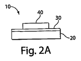
本発明によると、一度、水溶性犠牲層が形成され、関連構造材料が選択された位置で形成されると、犠牲層は、それから犠牲層を水と接触させ除去される。水への犠牲層の溶解は、SU8−2010フォトレジストディスクの配列が犠牲層に形成され、次に、犠牲層がディスクの剥離により除去されたプロセスを実行することにより実験的に検証された。図2Aに示すように、選択された水溶性重合体犠牲層30がケイ素基板20に沈着された後、SU8−2010フォトレジストのディスク40は、図2Aの断面図に示す構造10を形成するために、フォトリソグラフィーの単一ステップで犠牲層に直接パターン形成された。ディスク40の直径は、20μm〜1200μmの範囲であった。構造10は、それから、犠牲層30を剥離するために、水に浸漬された(図2B)。図3は、(a)PAAおよび(b)水中のデキストランの犠牲層の溶解により、SU8から作成された10μmの厚さのディスクを完全に剥離するために要する時間の作図である。エラーバーは、平均(n=3)からの偏差を示す。このデータは、PAA上に調製されたディスクが、デキストラン上に調製されたディスクより2倍速く剥離されたことを示す。
According to the present invention, once a water-soluble sacrificial layer is formed and the associated structural material is formed at a selected location, the sacrificial layer is then removed by contacting the sacrificial layer with water. The dissolution of the sacrificial layer in water was experimentally verified by performing a process in which an array of SU8-2010 photoresist discs was formed in the sacrificial layer, and then the sacrificial layer was removed by stripping the disc. After the selected water-soluble polymer
表2は、SiO2、リンケイ酸ガラス、ポリ(イミド)(例えば、HD Microsystems,Parlin,NJの熱的に加流されたP12610エポキシ樹脂)およびポジ形フォロレジスト(例えば、Clariant;Charlotte,NCのAZ1518、AZ4400およびAZ4620などのノボラックジアズキノンに基づく樹脂)などの犠牲層として使用された他のタイプと、PAAおよびデキストランの腐食速度の比較を示す。フィルムは、ポリ(エチレンオキシド)100kDa(1%w/v)、ポリ(メタクリル酸)(1.7%w/v)およびポリ(ビニルアルコール)(2.5%w/v)を含む水への溶解度が低い重合体を除く、5%(w/v)重合体溶液からスピンコーティング(3000rpm,15s)により調製された。次に、基板を2分間、150C° のホットプレートに設置して、フィルムを乾燥させたフィルムの均一性に関して、表2で使用されるように、用語「良い」は、3インチウェハ上に光学顕微鏡で検知可能な2つ以下の異質物の主観的な所見である。フィルム溶解度においては表2で使用されるように、用語「良い」は、1秒以下でフィルムが水に溶解することを示す。犠牲層の腐食速度は、剥離された物の幾何学構造に依存することを認識する。表2で表されるデータは、幾何学構造の依存を考慮に入れておらず、ガイドラインとしてのみ使用されるべきである。これらのデータは、水溶性犠牲層が、例えば、1%HF中のSiO2など、個々の腐食剤の従来の犠牲材料より最大4桁分速く水に溶解することを示す。他の材料と比較した水のPAAおよびデキストランの選択性も、ケイ素窒化物へのHFなどの従来の腐食剤のそれよりも非常に良好である。 Table 2 shows SiO 2 , phosphosilicate glass, poly (imide) (eg, thermally flowed P12610 epoxy resin from HD Microsystems, Parlin, NJ) and positive photoresist (eg, Clariant; Charlotte, NC). A comparison of the corrosion rates of PAA and dextran with other types used as sacrificial layers, such as resins based on novolak diazquinones such as AZ1518, AZ4400 and AZ4620). Films into water containing poly (ethylene oxide) 100 kDa (1% w / v), poly (methacrylic acid) (1.7% w / v) and poly (vinyl alcohol) (2.5% w / v) It was prepared by spin coating (3000 rpm, 15 s) from a 5% (w / v) polymer solution, excluding polymers with low solubility. Next, as used in Table 2, the term “good” refers to optical on a 3 inch wafer with respect to film uniformity, where the substrate was placed on a 150 ° C. hotplate for 2 minutes and the film was dried. It is a subjective finding of no more than two foreign objects that can be detected with a microscope. In film solubility, as used in Table 2, the term “good” indicates that the film dissolves in water in less than 1 second. It is recognized that the sacrificial layer corrosion rate depends on the geometry of the exfoliated object. The data represented in Table 2 does not take into account the dependence of the geometric structure and should only be used as a guideline. These data indicate that the water-soluble sacrificial layer dissolves in water up to four orders of magnitude faster than conventional sacrificial materials of individual corrosives, such as SiO 2 in 1% HF. The selectivity of water PAA and dextran compared to other materials is also much better than that of conventional corrosives such as HF to silicon nitride.
水溶性犠牲層のこの高い腐食選択性は、PAAがプラスチックディスクまたはITO被覆された基板上の犠牲層として使用された、さらなる剥離プロセスにより実験的に例証された。図4は、水に浸漬中、様々な時間間隔で、ITOフィルムで被覆されたPETシートのエポキシフォトレジスト(SU8−2010)で調製された200×200μm2の正方形カンチレバーのフィルム60の画像を示す。溶解境界部70は、剥離プロセス中のフィルム60のPAA除去の進行を示す。図4に示すように、約27秒内に、構造は、完全に切り取られている。この迅速な犠牲層の除去は、デキストラン層上で形成された重合したSU8の4cm2個体シートを使用した剥離プロセスによりさらに実験的に例証された。SU8シートは、水に約12時間基板を浸した後、完全に除去された。
This high corrosion selectivity of the water-soluble sacrificial layer was experimentally demonstrated by a further stripping process in which PAA was used as a sacrificial layer on a plastic disc or ITO coated substrate. FIG. 4 shows images of a
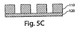
本発明によると、この迅速な水溶性重合体犠牲層の溶解は、最大ウェハサイズの距離を包含する微細構造フィルムの剥離に使用され得る。この能力は、金属フィルムのシャドー蒸着のマスクとして使用されたPAAフィルムのcm規模の構造のSU8で実験的に例証された。図5A〜Eは、プロセス中のステップの断面図を示す。図5Aに示すように、PAAフィルム100は、基板90に形成され、SU8層110は、PAAフィルム100にスピンコーティングされた後、構造80を形成するためにフォトリソグラフィーにより構成された。図5Bに示すように、PAAフィルム100は、水に溶解され、SU8層110は、剥離により回収された。シャドーマスクとして作用するSU8構造フィルム110は、第二の基板120に設置された(図5C)。金属の薄い層は、層130を形成するために金属蒸着によりサンプルに堆積された。ここで、層130は、PAAフィルム110の表面に形成された金属構造140、および基板120の表面に形成された金属構造150を含む。図5E、SU8層110が除去され、シャドーマスクの開口部を通して堆積された金属構造140のパターンが明らかになったところを示す。
According to the present invention, this rapid dissolution of the water-soluble polymer sacrificial layer can be used for peeling of microstructured films that encompass distances of maximum wafer size. This capability was experimentally demonstrated in SU8 with a cm-scale structure of PAA film used as a mask for shadow deposition of metal films. 5A-E show cross-sectional views of the steps in the process. As shown in FIG. 5A, the
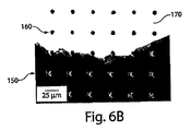
図6A〜Bは、図5のプロセスを使用して基板170に作られたAu形質の光学顕微鏡の画像を2つ示す。金の層は、五角形の開口部を有するマスク150に堆積された。マスク150は、図6Aに示すように、ピンセットで壊され、微便的に除去され、マスク150の開口部を通して基板170上に形成された金形質160を曝露した。図6Bは、金形質160を曝露するために部分的に除去されたマスク150の拡大画像を示す。金属堆積中、マスクと基板間に充分な接触を果たすために、広範囲(つまり、>10mm2)に渡り平面を維持するSU8シートを得ることが好まれることを認識する。
FIGS. 6A-B show two optical microscope images of Au traits made on the
本発明によると、水溶性重合体犠牲材料の溶解度は、イオン交換プロセスにより製造シーケンス中に選択的に変更され得る。水溶性フィルムの溶解度の容易性は、i)剥離による形質の迅速な剥離およびii)現在使用される腐食剤と非適合性である材料を含む仕様に対して有利である。しかし、水溶性フィルムの溶解度の容易性は、意図する除去の前に水溶液に犠牲材料を曝すことを必要とするマイクロ加工または他の製造プロセスに制限がある。本発明によると、この制限は、例えば、フィルムの水溶解度を低くするまたは削除するための、フィルムの水溶解度を変更する適切な化学物質で犠牲層を処理することにより克服され得る。次に、以下に記述するように、フィルムの水溶解度は、当該製造シーケンスで所望されるように回復され得る。 According to the present invention, the solubility of the water-soluble polymer sacrificial material can be selectively altered during the manufacturing sequence by an ion exchange process. The ease of solubility of water-soluble films is advantageous for specifications that include i) rapid release of traits due to release and ii) materials that are incompatible with currently used corrosive agents. However, the ease of solubility of water-soluble films is limited in microfabrication or other manufacturing processes that require the sacrificial material to be exposed to an aqueous solution prior to intended removal. According to the present invention, this limitation can be overcome by treating the sacrificial layer with a suitable chemical that alters the water solubility of the film, for example, to reduce or eliminate the water solubility of the film. Next, as described below, the water solubility of the film can be restored as desired in the manufacturing sequence.
例えば、PAAを含む犠牲層は、PAAが水に溶解するようにNa+などの一価のイオンと結合する(例えば、イオン結合などの結合の形成)側鎖を有し得る。PAA犠牲層は、PAAが水に不溶性になるように、PAAの側鎖が二価のイオンと結合するようCa+などの二価のイオンで処理され得る。犠牲材料が水溶液で可溶になり、よって、水溶液で処理することにより除去されるように、二価のイオンは、製造プロセス中、いつでも(例えば、Na+などの一価のイオンで処理することにより)ポリ(アクリル酸)から除去され得る。例えば、PAA犠牲層を考慮した場合、PAA重合体の側鎖は、(Na+)−カルボキシレート基を含む。Na+イオンがカルシウムイオンに交換された場合、PAA鎖は、ブリッジとなり、実質的に水不溶性PAA−Ca2+重合体を作り出す。本発明によると、カルシウムイオン源へのPAA犠牲層の曝露は、一時的に水不溶性になる犠牲層を作り出すために実行される。この溶解度の変更は、CuCl2およびCuSO4水溶液の形態でのCu2+などの他の二価のイオンでも達成することができる。しかし、Cr3+などの三価のイオンは、一般的に、PAAフィルムを水不溶性にしないことが実験的に分った。 For example, a sacrificial layer comprising PAA may have side chains that bind to monovalent ions such as Na + (eg, forming bonds such as ionic bonds) so that PAA dissolves in water. The PAA sacrificial layer can be treated with a divalent ion such as Ca + so that the side chain of PAA binds to the divalent ion so that PAA is insoluble in water. Divalent ions can be treated at any time during the manufacturing process (eg, with monovalent ions such as Na +) so that the sacrificial material is soluble in the aqueous solution and thus removed by treatment with the aqueous solution. Can be removed from the poly (acrylic acid). For example, when considering a PAA sacrificial layer, the side chain of the PAA polymer contains a (Na + ) -carboxylate group. When Na + ions are exchanged for calcium ions, the PAA chains become bridges, creating a substantially water-insoluble PAA-Ca 2+ polymer. According to the present invention, exposure of the PAA sacrificial layer to a calcium ion source is performed to create a sacrificial layer that becomes temporarily water insoluble. This change in solubility can also be achieved with other divalent ions such as Cu 2+ in the form of CuCl 2 and CuSO 4 aqueous solutions. However, it has been experimentally found that trivalent ions such as Cr 3+ generally do not render the PAA film water insoluble.
PAA層の溶解度は、例えば、選択された溶液中に層を浸すことにより変更される。例えば、PAA層は、1分間、1Mの水性CaCl2溶液に層を浸すことにより水不溶性になり得る。結果として生じたPAA−Ca2+層は、水中で少なくとも1時間安定することが分った。 The solubility of the PAA layer is altered, for example, by immersing the layer in a selected solution. For example, a PAA layer can become water insoluble by immersing the layer in 1 M aqueous CaCl 2 solution for 1 minute. The resulting PAA-Ca 2+ layer was found to be stable in water for at least 1 hour.
700nm以下の厚さのPAA層は、CaCl2の溶液に浸漬された場合、溶解せず、水不溶性であることが実験的に立証された。700nm以上の厚さのPAAフィルムも水不溶性であるが、下の基板または他の近くの材料への密着を失う可能性がある。例えば、シリコンウェハ上のPAAフィルムの接着を向上するために、例えば、酸性PAA(pH約2.5)溶液と調製された密着層を使用することが好ましい。 It has been experimentally demonstrated that a PAA layer with a thickness of 700 nm or less does not dissolve when immersed in a solution of CaCl 2 and is insoluble in water. A PAA film with a thickness of 700 nm or more is also water insoluble, but may lose adhesion to the underlying substrate or other nearby material. For example, in order to improve the adhesion of a PAA film on a silicon wafer, it is preferable to use, for example, an acidic PAA (pH about 2.5) solution and a prepared adhesion layer.
本技術の実験的例証において、5%(w/v)のPAA溶液は、基板にスピンコーティングされ、ホットプレートで15分間、150℃でベーキングされた。結果として生じた酸性PAAフィルムは、Siまたは石英で長時間ベーキング後、水不溶性になるが、一般的にガラスおよび金属被覆された表面でベーキングされた場合はそうではないことが分った。これらの知見は、Siウェハがその表面でSiO2の自然層を有する場合、PAA鎖がSiO2表面と共有結合を形成することを示唆する。約100℃以上で、エステルの形成は、蒸発による水の損失を通してケイ素のシラノールを用いたPAAのカルボキシル基の凝固により好まれることを理解されたい(R−COOH+R’−SiOH←→R−COO−Si−R’+H2O)。結果として生じたPAAフィルムは、もはや水に溶解されない。 In an experimental illustration of the technology, a 5% (w / v) PAA solution was spin coated onto a substrate and baked at 150 ° C. for 15 minutes on a hot plate. The resulting acidic PAA film was found to be water insoluble after prolonged baking with Si or quartz, but not generally when baked on glass and metallized surfaces. These findings suggest that the PAA chain forms a covalent bond with the SiO 2 surface when the Si wafer has a natural layer of SiO 2 on its surface. It should be understood that above about 100 ° C., ester formation is favored by the coagulation of the carboxyl group of PAA with silicon silanol through loss of water by evaporation (R—COOH + R′—SiOH ← → R—COO—). Si-R '+ H 2 O ). The resulting PAA film is no longer dissolved in water.
このような薄いベーキングされたPAAフィルムを適正位置に用いて、中性pH溶液から堆積した第二のPAAフィルムが、次に、第一フィルムの上に形成され得る。次に、上部PAAフィルムは、その溶解度を変更するために、CaCl2溶液を用いて処理され得る。最大9μmの厚さのPAAフィルムの水性溶解は、この2ステップ手順により阻止され得ることが実験的に立証された。 Using such a thin baked PAA film in place, a second PAA film deposited from a neutral pH solution can then be formed on the first film. The upper PAA film can then be treated with a CaCl 2 solution to change its solubility. It has been experimentally demonstrated that aqueous dissolution of PAA films up to 9 μm thick can be prevented by this two-step procedure.
本発明によると、一度水溶性犠牲層が水に不溶性になると、製造ステップまたは層の水への曝露を伴うステップが実行され、次に、犠牲層が再び水溶性になり、それによって水への最終曝露により層が除去可能になる。例えば、不溶性PAA−Ca2+層は、NaCl([NaCl]=10mM〜1M)溶液に浸漬することにより再び水溶性になり得る。溶液中のナトリウムイオンの過剰は、PAA−Ca2+フィルムのカルシウムイオンを置き換え、>10mMNaCl溶液に1秒以内にカルシウム交換したPAAフィルムを溶解する。 According to the present invention, once the water-soluble sacrificial layer is insoluble in water, a manufacturing step or a step involving exposure of the layer to water is performed, and then the sacrificial layer is again water-soluble, thereby causing water The final exposure allows the layer to be removed. For example, an insoluble PAA-Ca 2+ layer can be rendered water soluble again by immersing it in a NaCl ([NaCl] = 10 mM to 1 M) solution. The excess of sodium ions in the solution displaces the calcium ions of the PAA-Ca 2+ film and dissolves the exchanged PAA film in> 10 mM NaCl solution within 1 second.
PAA−Ca2+フィルムは、水に完全に不溶性であるが、100μMのNaCl5pH4HClまたはpH9NaOHなどの塩類の水溶液中で、唯一、限られた安定性(例えば、約5分間の浸漬)をもつことが実験的に立証された。しかし、他の塩類の水性溶液にさらにCaCl2を追加すると、数桁分、PAA−Ca2+フィルムの安定性を向上する。例えば、PAA−Ca2+フィルムは、およそ等モル量のCa2+イオンを含む500mMのNaCl溶液中で、数時間、不溶性を維持することができる。より一般的には、全ての一価カチオンの合計に対する溶液中の0.1等量Ca2+の存在は、PAA−Ca2+フィルムの不溶性を維持するのに充分であることが分る。
PAA-Ca 2+ films are completely insoluble in water, but have only limited stability (eg, immersion for about 5 minutes) in aqueous solutions of salts such as 100
しかし、このアプローチは、カルシウムイオンがCa(OH)2の形態で沈殿し、PAAイオンブリッジを維持するための高濃度を効果的に維持できないので、強いアルカリ溶液中で効果を立証しないかもしれない。結果として、12〜13のpH値をもつアルカリ性展開剤(Shipleyポジ型フォトレジストに使用される351展開剤など)は、現在、PAA犠牲フィルムと非適合性である。 However, this approach may not prove effective in strong alkaline solutions because calcium ions precipitate in the form of Ca (OH) 2 and cannot effectively maintain high concentrations to maintain the PAA ion bridge. . As a result, alkaline developing agents with pH values of 12-13 (such as 351 developing agents used in Shipley positive photoresists) are currently incompatible with PAA sacrificial films.
本発明によると、その水溶性を変更するためのPAAなどのイオンブリッジの水溶性重合体の有用性は、金属形質がPAAの構成されたフィルムを通してニッケルの電着により製造される実験的実施例により示される。この実施例は、犠牲層自体が選択された構造を作成するためにパターン形成されることをさらに示す。 In accordance with the present invention, the utility of water soluble polymers of ion bridges such as PAA for altering its water solubility is an experimental example in which the metal trait is produced by nickel electrodeposition through a PAA structured film. Indicated by. This example further shows that the sacrificial layer itself is patterned to create the selected structure.
図7Aに示すように、ITO被覆されたポリエチレンテレフタレート(PET)基板180は、PAA−Ca2+層190を生成するために処理されたPAAフィルムで被覆された。SU8領域200および202は、構造を定義するためのフォトレジストとして形成された(図7B)。図7Cに示すように、PAA−Ca2+層190は、PAA−Ca2+構造192および194を形成するためにSU8のフォト構成されたフィルムの開口部を通して、NaClを用いて選択的にPAA−Ca2+層190を溶解することによりパターン形成された。SU8マスク(例えば、SU8領域200および202を含む)は、次に、NMPに浸漬することにより除去された(図7D)。水溶液がSU8の表面を湿潤したことを確実にするために、洗剤(0.05%Tween)を含んだ1MNaClとして腐食剤を提供した。次に、PAA−Ca2(例えば、PAA−Ca2+構造192および194を含む)の曝露フィルムに達するために、生理用食塩水をSU8の小さな直径(つまり、<50μm)の開口部を通して浸透させた。一般的に、重合したSU8の除去は難しく、剥離層の適用を必要とする。本実験的実施例において、SU8は、シリコンウェハの表面からより非常に迅速(つまり、1時間以内)にPAAベースフィルムから除去されることが分った。従って、本発明によると、SU8を直接基板に使用するより、SU8マスクを使用したPAAベースフィルムなどの犠牲層をパターン形成するのがより簡単であることが理解される。これは、本発明の犠牲層の利点および有用性をさらに提供する。
As shown in FIG. 7A, an ITO coated polyethylene terephthalate (PET)
結果として得たPAA−Ca2+構造192および194を用いて、ニッケルは、ニッケル層210を形成するために1または20mAcm−2の電流でスルファミン酸ニッケルの商業用溶液に基板を浸漬することにより電気メッキされた(図7E)。基板180は、パターン形成されたPAA−Ca2+(例えば、PAA−Ca2+構造192および194を含む)の開口部に金属の堆積に必要な電流を適切に導電することが分った。堆積が完了した後、PAA−Ca2+構造192および194は、上述のNaCl溶液中で腐食することにより除去された(図7F)。
Using the resulting PAA-Ca 2+ structures 192 and 194, nickel is electroplated by immersing the substrate in a commercial solution of nickel sulfamate at a current of 1 or 20 mA cm −2 to form the
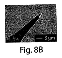
図8Aは、低倍率および高倍率の両方での、ニッケル層210のエッジ解析のSEM画像を示す。図8Bは、ニッケル層210の横方向解析のSEM画像を示す。SEM画像は、ニッケル形質のために処理されたエッジの粗さおよび横方向解析が、SU8の初期層をパターン形成するのに使用された透明フォトマスクのそれに類似している(つまり、約8μmの解析)ことを示す。ニッケルイオンは、Ca2+カチオンのように二価であり、PAA−Ca2+構造192および194を溶解できない。PAA−Ca2+構造層は、エレクトロニクス分野の用途用の「すぐに使用可能な」溶液の形で商業的に入手可能なスルファミン酸ニッケルの溶液中、40℃で少なくとも3時間、安定した。PAA−Ca2+構造192および194のこの安定性は、図8Cで示す5μmの厚さの構造などの厚い形質のニッケルの調製を可能にする。
FIG. 8A shows an SEM image of the edge analysis of the
図8AのSEM画像で示すようなニッケル形質のエッジ解析および図8BのSEM画像で示すような横方向解析は、フォトリソグラフィーに使用された透明マスクにより判断された。ニッケルの領域は、SEM画像で明るく見える。図7IのSEMにより検証されるように、PAA−Ca2+構造は、厚いニッケル形質の電子構成中、長時間(40℃で>3時間)、スルファミン酸ニッケルの商業用溶液で安定した。 Edge analysis of nickel traits as shown in the SEM image of FIG. 8A and lateral analysis as shown in the SEM image of FIG. 8B were judged by the transparent mask used for photolithography. The nickel area appears bright in the SEM image. As verified by the SEM in FIG. 7I, the PAA-Ca 2+ structure was stable in a commercial solution of nickel sulfamate for an extended period (> 3 hours at 40 ° C.) during the thick nickel-trait electronic configuration.
本発明によると、例えば、マイクロ規模の表面マイクロ加工構造などの自立スタンドMEMS構造は、犠牲層としてPAAおよびデキストランのような水溶性重合体のフィルムを使用して製造され得る。犠牲層の腐食状態が特に軽い場合、本発明の製造方法は、半導体、金属、重合体および他のマイクロエレクトロニクス材料を含む、多様なマイクロエレクトロニクス材料と適合する。 In accordance with the present invention, free standing stand MEMS structures such as, for example, microscale surface microfabricated structures can be fabricated using films of water soluble polymers such as PAA and dextran as sacrificial layers. If the sacrificial layer is particularly corrosive, the manufacturing method of the present invention is compatible with a variety of microelectronic materials, including semiconductors, metals, polymers, and other microelectronic materials.
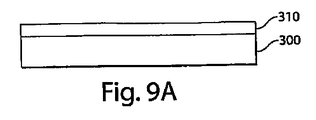
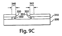
図9は、PET、SU8およびアルミニウムがカンチレバーおよび基板の表面に対する水溶性犠牲層により支持されたブリッジ構造の製造に使用される、自立スタンド構造製造の実験的実施例を示す。例示的な実施形態において、犠牲層310(例えば、PAA−Ca2+層)は、図9Aに示すように、基板300上に形成される。SU8フィルムは、犠牲層310上に形成され、SU8領域320および322を形成するために、SU8フォトリソグラフィーを使用してパターン形成される(図9B)。犠牲層310は、本明細書で記述されるように、それぞれ自立スタンド長340および342をもつSU8構造330および332を形成するために除去され得る。自立スタンド構造330および332は、それぞれスペース350および352により、基板300から分離される。いくつかの場合において、PET基板上の距離が>500μmの範囲であるブリッジは、図9に示すように、形成され得る。
FIG. 9 shows an experimental example of self-supporting stand construction where PET, SU8 and aluminum are used to make a bridge structure supported by a water-soluble sacrificial layer on the cantilever and substrate surface. In the exemplary embodiment, a sacrificial layer 310 (eg, a PAA-Ca 2+ layer) is formed on the
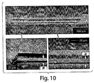
本表面マイクロ加工技術において、犠牲層は、小さい形質が自立スタンドになる(約40s)まで、水中で腐食されるが、大きい構造は、下の無処理の犠牲層の基板に結合されたままである。図10は、19%w/vでのPAA溶液を用いたPAA犠牲層を使用してPETシート上に作成された80μm幅のSU8ブリッジのSEM画像を提供する。本プロセスで使用された全ての材料は、有機重合体を絶縁するため、10nmの厚さの金フィルムがSEMの観察を可能にするため、サンプル上に提供された。図11は、20%w/vでのデキストラン溶液を用いたデキストランフィルムを使用してSi上に調製されたSU8のカンチレバーのSEM画像である。SU8カンチレバーの形質は、図4のものと同一である。 In this surface micromachining technique, the sacrificial layer is eroded in water until the small trait becomes a freestanding stand (about 40 s), but the large structure remains bonded to the underlying untreated sacrificial layer substrate. . FIG. 10 provides an SEM image of an 80 μm wide SU8 bridge created on a PET sheet using a PAA sacrificial layer with a 19% w / v PAA solution. All materials used in the process were provided on the sample to insulate the organic polymer so that a 10 nm thick gold film would allow SEM observation. FIG. 11 is a SEM image of a SU8 cantilever prepared on Si using a dextran film with a dextran solution at 20% w / v. The character of SU8 cantilever is the same as that of FIG.
柔軟な重合材料は、マイクロ製造に基板として使用される場合、Young率が製造構造の設計において考慮されなければならないことに留意されたい。例えば、10μmの厚さのPAA層の厚い犠牲層を焼く間に基板に生じるストレスは、PETシートなどの柔軟な基板を変形する可能性がある。基板の変形を削減するために、焼成中、基板のエッジに力を加え得る。例えば、約50gの金属おもりが基板の周辺に沿って設置され得る。サブミクロンの厚さの犠牲層を使用した場合、基板の変形は生じない。 It should be noted that when the flexible polymer material is used as a substrate in micro-manufacturing, the Young's factor must be considered in the design of the manufacturing structure. For example, stress generated on the substrate while baking a thick sacrificial layer of 10 μm thick PAA layer can deform a flexible substrate such as a PET sheet. To reduce the deformation of the substrate, force may be applied to the edge of the substrate during firing. For example, about 50 g of metal weight can be placed along the periphery of the substrate. If a submicron thick sacrificial layer is used, no deformation of the substrate occurs.
剥離されたつり構造と基板の間のファンデルワールス力により生じる静摩擦の問題は、周知である。本発明によると、この静摩擦は、剥離に使用される水が蒸発する時、つり構造の基板への圧壊を避けるために、軽減または阻止され得る。静摩擦を避けるための例示的剥離方法において、一度水溶性犠牲層が構造から充分に除去されたら、腐食プロセスを停止するために、好ましくは即時に基板をイソプロパノールで洗浄し、それから、つり構造の剥離による表面張力を低下するためにヘキサンで洗浄することが望ましい場合、次に、さらなる圧壊を防止するために自立スタンド構造を乾燥させる。 The problem of static friction caused by van der Waals forces between the detached suspended structure and the substrate is well known. According to the present invention, this static friction can be reduced or prevented to avoid crushing the suspension structure to the substrate when the water used for stripping evaporates. In an exemplary stripping method to avoid static friction, once the water-soluble sacrificial layer has been sufficiently removed from the structure, the substrate is preferably immediately washed with isopropanol to stop the corrosion process, and then the suspension structure is stripped. If it is desired to wash with hexane to reduce the surface tension due to, then the free standing stand structure is dried to prevent further crushing.
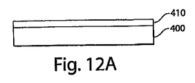
本発明は、導電性形質を含む自立スタンド構造の製造をさらに提供する。図9に示す技法に基づく本プロセスの実験的なデモンストレーションのマイクロ製造ステップの略図を図12に示す。犠牲層410は、基板400(図12A)上に形成され、領域420および422をもつパターン形成されたSU8層は、犠牲層410(図12B)上に形成される。導電性形質を生成するために、図12Cに示すように、金属層領域430、432および434を含む50nmアルミニウムフィルムなどの金属フィルムを、構造材料(SU8など)または他の選択されたマイクロエレクトロニクス材料上で蒸発させた後、図12Dに示すように、犠牲層410が除去されると金属が剥離される腐食プロセスが実行される。図913は、19%w/vでPAA犠牲層を使用してSiウェハ上に調製された導電性ブリッジおよびSU8微細構造上のフィルムの側面図を示すSEM図を提供する。
The present invention further provides for the manufacture of a freestanding stand structure that includes conductive traits. A schematic diagram of the microfabrication steps of an experimental demonstration of the process based on the technique shown in FIG. 9 is shown in FIG. A
アルミニウムフィルムは、PAAへの密着が不十分であるが、SU8構造材料には強固に密着するため、本プロセスは、特にPAA犠牲層の使用に適している。水との接触において、PAA層上のアルミニウムフィルムは、PAA表面から急速に分離するフレークを形成し、下にあるPAAフィルムを明らかにする。音波処理浴に基板を浸漬して、金属被覆されたSU8機械構造に損傷を与えることなくPAA層上の全てのアルミニウムを5秒以内で除去する。その後、図9Bに示すように、PAA犠牲層を腐食するために、自立スタンド構造が約40秒で基板から剥離されるまで、基板を水中に放置し得る。逆に、蒸発させたアルミニウムは、デキストランによく密着し、水中でのアルミニウムの剥離は、SU8の金属被覆された形質を剥離するのに必要とされる時間より遅い。これは、i)フィルムの厚さの可能範囲がデキストランよりPAAの方が大きい、ii)PAAフィルムの溶解度は、Ca2+またはCu2+カチオンの添加により化学的に調節され得る、およびiii)金属フィルム密着がPAAに弱いため導電性形質の調製が可能である、という3つがデキストランよりPAAを使用する主な利点であることを本発明により分ることを強調する。 The aluminum film has insufficient adhesion to the PAA, but adheres firmly to the SU8 structural material, so the process is particularly suitable for use with a PAA sacrificial layer. In contact with water, the aluminum film on the PAA layer forms flakes that rapidly separate from the PAA surface, revealing the underlying PAA film. The substrate is immersed in a sonication bath to remove all aluminum on the PAA layer within 5 seconds without damaging the metallized SU8 mechanical structure. Thereafter, as shown in FIG. 9B, the substrate can be left in water until the free standing structure is peeled from the substrate in about 40 seconds to corrode the PAA sacrificial layer. Conversely, the evaporated aluminum adheres well to dextran, and the stripping of the aluminum in water is slower than the time required to strip the SU8 metallized trait. This is because i) the possible range of film thickness is greater for PAA than dextran, ii) the solubility of the PAA film can be chemically adjusted by the addition of Ca 2+ or Cu 2+ cations, and iii) metal films It is emphasized that the present invention shows that the three main advantages of using PAA over dextran are that it is possible to prepare conductive traits due to weak adhesion to PAA.
上述の実験的実施例において、材料を以下のように得た。PAA50kDaおよびポリ(メタクリル酸)は、Polysciences(Warrington,PA)から購入した。デキストラン66kDa、キトサン、ポリ(エチレンオキシド)2kDa、ポリ(ビニルアルコール)およびポリ(エチレンイミン)は、Sigma−Aldrich(St.Louis,MO)から得た。PAA2kDa、ポリ(エチレンオキシド)100kDaおよびポリ(アクリルアミド)は、Sp2(Scientific Polymer Products Inc.,Ontario,NY)から得た。SU8−2010フォトレジストは、Microchem(Newton,MA)から購入した。ITO被覆PET基板(200μmの厚さ、Rs<10Ω)は、Delta Technologies(Stillwater,MN)から得、非被覆PET基板(約100μmの厚さ)は、Policrom(Bensalem,PA)から得た。 In the above experimental example, the material was obtained as follows. PAA 50 kDa and poly (methacrylic acid) were purchased from Polysciences (Warrington, Pa.). Dextran 66 kDa, chitosan, poly (ethylene oxide) 2 kDa, poly (vinyl alcohol) and poly (ethyleneimine) were obtained from Sigma-Aldrich (St. Louis, MO). PAA 2 kDa, poly (ethylene oxide) 100 kDa and poly (acrylamide) were obtained from Sp 2 (Scientific Polymer Products Inc., Ontario, NY). SU8-2010 photoresist was purchased from Microchem (Newton, Mass.). ITO coated PET substrates (200 μm thickness, Rs <10Ω) were obtained from Delta Technologies (Stillwater, MN), and uncoated PET substrates (approximately 100 μm thickness) were obtained from Polyrom (Bensalem, PA).
実験的実施例で記述される形状測定結果は、Tencor(San Jose,CA)からのαステップ200を用いて得た。電着のニッケル源は、Technic Inc.(Providence,RI)から購入したすぐに使用可能な(RTU)溶液、“S”スルファミン酸ニッケルであった。電着に適用される電流は、Princeton Applied Research(Oak Ridge,TN)の発電機Pentiostat/Galvanostatモデル273を用いて調節された。フォトリソグラフィー用のフォトマスクは、CAD/Arts(Poway,CA)から得た。
The shape measurement results described in the experimental examples were obtained using an
犠牲層調製の実験的実施例は、以下の手順を使用した。水中の25%(w/v)溶液として購入したPAAは、pHインジケータバンドテストを用いて7.5のpHに達するまで、NaOHの飽和溶液で中和され、次に、適切な濃度に稀釈された。デキストラン溶液は、適切なデキストランと水をバイアルで混合して調製され、デキストランの完全溶解は、バイアルを温水浴(90〜95℃)に設置して得た。シリコンウェハを、5%のHCl水溶液に5分間浸漬し、脱イオン水で洗浄して、窒素ガス流で乾燥させた。PET基板などの重合基板の表面は、酸素プラズマに短時間曝露して(30s,18W)親水性にした。これらの処理は、両方、PAA水溶液および基板上のデキストランの湿潤性を向上した。 The experimental procedure for sacrificial layer preparation used the following procedure. PAA purchased as a 25% (w / v) solution in water is neutralized with a saturated solution of NaOH until a pH of 7.5 is reached using the pH indicator band test and then diluted to the appropriate concentration. It was. A dextran solution was prepared by mixing appropriate dextran and water in a vial, and complete dissolution of dextran was obtained by placing the vial in a warm water bath (90-95 ° C.). The silicon wafer was immersed in 5% aqueous HCl for 5 minutes, washed with deionized water, and dried with a stream of nitrogen gas. The surface of a polymerization substrate such as a PET substrate was exposed to oxygen plasma for a short time (30 s, 18 W) to make it hydrophilic. Both of these treatments improved the wettability of the PAA aqueous solution and dextran on the substrate.
水溶性重合体の溶液を(5%(w/v)以下または以上の重合体溶液に対して、それぞれ0.45μmまたは5μmの孔サイズ)濾過し、表面の約90%が溶液で覆われるまで基板に分配した。犠牲層は、次に、15秒間、1000〜4000rpmで基板をスピンコーティングすることにより調製され、ホットプレートで(ケイ素は150℃で、重合体基板は95℃で)2分間フィルムをベーキングした。 Filter the water-soluble polymer solution (0.45 μm or 5 μm pore size for 5% (w / v) or higher polymer solution, respectively) until about 90% of the surface is covered with the solution. Distributed to the substrate. The sacrificial layer was then prepared by spin coating the substrate at 1000-4000 rpm for 15 seconds, and the film was baked on a hot plate (150 ° C. for silicon and 95 ° C. for the polymer substrate) for 2 minutes.
上の実験的実施例に記述するフォトレジスト構造は、製造者の説明書に従い調製された。PAAおよびデキストランの腐食速度の特性、Ni電着を用いた実験、および金属、犠牲層のシャドーマスク蒸発は、5%(w/v)の重合体溶液および3000rpmでのスピンコーティングにより調製された。自立スタンド犠牲層は、19%のPAAおよび20%デキストラン(w/v)の溶液、および1000rpmでのスピンコーティングにより調製された。犠牲層の腐食の特性は、脱イオン水を用いて実行された。他の全ての実験において、SU8形質上の水(またはNaCl溶液)の湿潤性を向上するために、0.05%の濃度のTween20が添加された。ニッケルは、1および20mAcm−2の間の一定の電流で電着された。自立スタンド形質は、40秒間水に浸漬することにより剥離された
The photoresist structures described in the experimental examples above were prepared according to the manufacturer's instructions. The corrosion rate characteristics of PAA and dextran, experiments with Ni electrodeposition, and shadow mask evaporation of metals, sacrificial layers were prepared by 5% (w / v) polymer solution and spin coating at 3000 rpm. A free-standing sacrificial layer was prepared by 19% PAA and 20% dextran (w / v) solution and spin coating at 1000 rpm. The sacrificial corrosion characteristics were performed using deionized water. In all other experiments, 0.05% concentration of

特許請求の範囲(上記明細書と同様)において、「構成する」、「含む」、「もつ」、「有する」、「含有する」、「からなる」、「作る」、「形成する」、「関与する」などの全ての移行句または含蓄の句は、制限がない、つまり、「含むが制限されない」という意味と解釈されるべきであり、よって、それ以降に挙げられる項目、およびその等価物だけでなく追加項目も含む。移行句または含蓄の慣用句である「一致する」および「本質的に一致する」のみが、それぞれ、制限または半制限と解釈されるよう明確に指示されなければ、本明細書および特許請求の本明細書で使用されるように、単数の表現は、「少なくとも1つ」の意味であることを理解するべきである。 In the claims (similar to the above specification), “comprise”, “include”, “have”, “have”, “contain”, “consist of”, “make”, “form”, “ All transitional or connotational phrases such as “involved” should be construed as unrestricted, that is, mean “including but not limited”, and thus the items listed below and their equivalents. As well as additional items. Unless the transitional or implied idioms “match” and “essentially match” only are specifically instructed to be construed as limitations or semi-limits, respectively, As used in the specification, the singular expression should be understood to mean “at least one”.
本明細書の記載および特許請求の範囲で使用されるように、句「および/または」は、そのように結合された要素の「いずれ、または、両方」、つまり、ある場合において結合的に存在し、また他の場合において選言的に存在する要素を意味することを理解するべきである。他の要素は、特に定義されたこれらの要素に関連するまたは関連しないに関わらず、「および/または」句により特に定義された要素以外に任意で存在し得る。従って、制限されない実施例として、「Aおよび/またはB」に参照は、ある実施形態において、Aのみ(任意にB以外の要素を含む)、他の実施形態において、Bのみ(任意にA以外の要素を含む)、また他の実施形態において、AおよびBの双方(任意に他の要素を含む)等を意味する。本明細書の記載および特許請求で使用されるように、「または」は、上述の「および/または」と同様の意味をもつことを理解するべきである。例えば、リストの項目を分類する場合、「または」または「および/または」は、包括的、つまり、要素の数またはリストの少なくとも1つを含むが、一つ以上も含み、任意に追加のリストされていない項目も含むと解釈され得る。逆に「一つのみ」または「まさに一つ」などの明確に示される唯一の用語は、要素の数またはリストのまさに一要素を含むことを意味する。一般的に、本明細書で使用されるように、用語「または」は、「いずれか」、「一つ」、「一つのみ」または「まさに一つ」などの排他性の用語に先行される場合、排他的な代替(つまり、「一方またはもう一方であるが、両方ではない」)を示すようにのみ解釈されるべきである。 As used herein in the description and in the claims, the phrase “and / or” refers to “any or both” of the elements so conjoined, that is, in some cases conjointly present. And should be understood to mean elements that are disjunctive in other cases. Other elements may optionally be present other than those specifically defined by the “and / or” phrase, whether or not specifically related to these elements as defined. Thus, as a non-limiting example, reference to “A and / or B” refers to, in some embodiments, only A (optionally including elements other than B), and in other embodiments, only B (optionally other than A). In other embodiments, both A and B (optionally including other elements) and the like are meant. As used in the description and claims herein, it is to be understood that “or” has the same meaning as “and / or” described above. For example, when classifying items in a list, “or” or “and / or” is inclusive, ie includes at least one of a number of elements or a list, but also includes one or more, optionally additional lists It may be construed to include items that are not. Conversely, a distinct term such as “only one” or “exactly one” is meant to include the number of elements or exactly one element of a list. In general, as used herein, the term “or” precedes an exclusive term such as “any”, “one”, “only one” or “exactly one”. Cases should be construed only to indicate exclusive alternatives (ie, “one or the other but not both”).
本明細書の記載および特許請求の範囲で使用されるように、句「少なくとも一つ」は、一つ以上の要素のリストに関して、特に示されない限り、要素リストの要素のいずれかまたは一つ以上から選択された少なくとも一つの要素だが、必ずしも要素リスト内に特定的に挙げられた各および全ての要素の少なくとも一つを含むとは限らず、要素リストの要素のいずれの組み合わせを除外しないと理解されるべきである。この定義は、特定的に同定された要素に関連するまたはしないに関わらず、要素が、句「少なくとも一つ」が意味する要素のリスト内で特定的に同定された要素以外に任意に存在し得ることも可能にする。従って、制限されない実施形態のように、「少なくともAおよびBの一つ」(または同等に「AまたはB」、または同等に「Aおよび/またはB」)は、ある実施形態において、任意で一つ以上を含む少なくともBの存在を伴わないAの一つ(および任意でB以外の要素を含む)、他の実施形態において、任意で一つ以上を含む少なくともAの存在を伴わないBの一つ(および任意でA以外の要素を含む)、また他の実施形態において、任意で一つ以上を含む少なくともAの一つおよび任意で一つ以上を含む少なくともB(および任意で他の要素を含む)等を意味する。 As used in the description and claims herein, the phrase “at least one” relates to a list of one or more elements, unless stated otherwise, any one or more of the elements of the element list. At least one element selected from but does not necessarily include at least one of each and every element specifically listed in the element list and is understood not to exclude any combination of elements from the element list It should be. This definition is optional as long as the element is not specifically identified in the list of elements that the phrase “at least one” means, regardless of whether it is related to or not specifically identified. It also makes it possible to get. Thus, as in a non-limiting embodiment, “at least one of A and B” (or equivalently “A or B”, or equivalently “A and / or B”) is optional in some embodiments. One of A without the presence of at least B including one or more (and optionally including elements other than B), and in another embodiment of one of B without the presence of at least A optionally including one or more (And optionally including elements other than A), and in other embodiments, at least one of optionally including one or more and at least B of optionally including one or more (and optionally including other elements) Means).
特許および開示された出願を含む本明細書で引用された参考文献の全ては、本明細書中に参考として援用される。本明細書および参考文献として引用したおよび/または本明細書で引用した資料が、開示に対立する、および/または矛盾した用語の使用および/または引用/参考文献の使用または本明細書で使用または定義されたものと異なる用語の定義を含む場合、本明細書が優先する。 All references cited herein, including patents and disclosed applications, are hereby incorporated by reference. Documents cited and / or cited herein as references in this specification and / or references are used in terms of conflicting and / or contradictory disclosure and / or use of / quoted / references or used herein. In case of including a definition of a term that differs from that defined, the present specification shall control.
Claims (28)
重合体を含む犠牲材料を基板に形成するステップであって、前記重合体は、前記製造プロセスで使用される、少なくとも1つの溶媒に対するある溶解度を持つステップと、
前記溶媒に対する前記重合体の前記溶解度を変更するために前記重合体を処理するステップと、
犠牲材料として前記重合体を使用して、製造プロセスを実行するステップと、
少なくとも部分的に前記重合体を前記溶媒に溶解することにより、前記重合体を除去するステップと、を含む方法。 A method of micro-manufacturing process or other small-scale manufacturing process,
Forming a sacrificial material comprising a polymer on a substrate, the polymer having a certain solubility in at least one solvent used in the manufacturing process;
Treating the polymer to change the solubility of the polymer in the solvent;
Performing a manufacturing process using the polymer as a sacrificial material;
Removing the polymer by at least partially dissolving the polymer in the solvent.
水溶液に可溶性である重合体を含む犠牲材料を基板に形成するステップと、
前記重合体が水溶液に実質的に不溶性になるように、二価のイオンで前記犠牲材料を処理するステップと、
前記重合体が水溶液に可溶となるように、前記犠牲材料から二価のイオンを除去するステップと、
前記犠牲材料を除去するステップと、を含む方法。 A method of micro-manufacturing process or other small-scale manufacturing process,
Forming on the substrate a sacrificial material comprising a polymer that is soluble in an aqueous solution;
Treating the sacrificial material with divalent ions such that the polymer is substantially insoluble in an aqueous solution;
Removing divalent ions from the sacrificial material such that the polymer is soluble in an aqueous solution;
Removing the sacrificial material.
ポリ(アクリル酸)を含む前記犠牲材料を基板に形成するステップであって、前記ポリ(アクリル酸)が一価のイオンと会合しており、前記犠牲材料が水溶液に可溶性である、ステップと、
前記ポリ(アクリル酸)が二価のイオンと会合し、犠牲材料が水溶液に実質的に不溶性になるように、前記二価のイオンで前記犠牲材料を処理するステップと、
犠牲材料として前記ポリ(アクリル酸)を使用して製造プロセスを実行するステップと、
前記犠牲材料が水溶液に可溶となるように、前記ポリ(アクリル酸)から二価のイオンを除去するステップと
前記犠牲材料を除去するステップと、を含む方法。 A method of micro-manufacturing process or other small-scale manufacturing process,
Forming the sacrificial material comprising poly (acrylic acid) on a substrate, wherein the poly (acrylic acid) is associated with monovalent ions and the sacrificial material is soluble in an aqueous solution;
Treating the sacrificial material with the divalent ions such that the poly (acrylic acid) associates with the divalent ions and the sacrificial material is substantially insoluble in an aqueous solution;
Performing a manufacturing process using the poly (acrylic acid) as a sacrificial material;
Removing the divalent ions from the poly (acrylic acid) so that the sacrificial material is soluble in an aqueous solution; and removing the sacrificial material.
前記重合体を第一のイオン交換反応に供することにより、前記溶媒に対する前記重合体の溶解度を下げるために、前記重合体を処理するステップと、
前記重合体を犠牲材料として使用して、前記製造プロセスを実行するステップと、
製造後、前記重合体を第二のイオン交換反応に供することにより、前記溶媒に対する前記重合体の溶解度を上げるために、前記重合体を処理するステップと、
少なくとも部分的に前記重合体を前記溶媒に溶解することにより、前記重合体を除去するステップと、を含む、請求項1に記載の方法。 The solvent is an aqueous solution, and the method includes:
Treating the polymer to reduce the solubility of the polymer in the solvent by subjecting the polymer to a first ion exchange reaction;
Performing the manufacturing process using the polymer as a sacrificial material;
After production, treating the polymer to increase the solubility of the polymer in the solvent by subjecting the polymer to a second ion exchange reaction;
2. The method of claim 1, comprising removing the polymer by at least partially dissolving the polymer in the solvent.
Applications Claiming Priority (2)
| Application Number | Priority Date | Filing Date | Title |
|---|---|---|---|
| US67141505P | 2005-04-14 | 2005-04-14 | |
| PCT/US2006/014184 WO2006113492A2 (en) | 2005-04-14 | 2006-04-14 | Adjustable solubility in sacrificial layers for microfabrication |
Publications (1)
| Publication Number | Publication Date |
|---|---|
| JP2008536699A true JP2008536699A (en) | 2008-09-11 |
Family
ID=36844587
Family Applications (1)
| Application Number | Title | Priority Date | Filing Date |
|---|---|---|---|
| JP2008506776A Pending JP2008536699A (en) | 2005-04-14 | 2006-04-14 | Tunable solubility in sacrificial layers for microfabrication |
Country Status (6)
| Country | Link |
|---|---|
| US (1) | US8357616B2 (en) |
| EP (1) | EP1877863A2 (en) |
| JP (1) | JP2008536699A (en) |
| KR (1) | KR20070120605A (en) |
| CN (1) | CN101176040A (en) |
| WO (1) | WO2006113492A2 (en) |
Cited By (2)
| Publication number | Priority date | Publication date | Assignee | Title |
|---|---|---|---|---|
| WO2010038579A1 (en) * | 2008-09-30 | 2010-04-08 | ソニー株式会社 | Process for producing microbeads and microbeads |
| JPWO2018061323A1 (en) * | 2016-09-30 | 2019-07-11 | 株式会社ジーシー | Method of manufacturing bioabsorbable membrane and bioabsorbable membrane |
Families Citing this family (27)
| Publication number | Priority date | Publication date | Assignee | Title |
|---|---|---|---|---|
| JP2008225417A (en) * | 2007-03-16 | 2008-09-25 | Fujitsu Ltd | Manufacturing method for structure |
| US7719752B2 (en) | 2007-05-11 | 2010-05-18 | Qualcomm Mems Technologies, Inc. | MEMS structures, methods of fabricating MEMS components on separate substrates and assembly of same |
| JP5292398B2 (en) * | 2007-07-09 | 2013-09-18 | イー・アイ・デュポン・ドウ・ヌムール・アンド・カンパニー | Compositions and methods for manufacturing electronic circuit structures |
| US8475924B2 (en) | 2007-07-09 | 2013-07-02 | E.I. Du Pont De Nemours And Company | Compositions and methods for creating electronic circuitry |
| US7749903B2 (en) * | 2008-02-07 | 2010-07-06 | International Business Machines Corporation | Gate patterning scheme with self aligned independent gate etch |
| US10570005B2 (en) * | 2008-12-16 | 2020-02-25 | Massachusetts Institute Of Technology | Method and apparatus for release-assisted microcontact printing of MEMS |
| US9458357B2 (en) | 2011-03-02 | 2016-10-04 | Massachusetts Institute Of Technology | ph-sensitive sacrificial materials for the microfabrication of structures |
| KR20120119167A (en) * | 2011-04-20 | 2012-10-30 | 삼성전기주식회사 | Method of manufacturing inertial sensor |
| ITMI20110995A1 (en) | 2011-05-31 | 2012-12-01 | Ione | METHOD FOR THE PRODUCTION OF MONOLITHIC THREE-DIMENSIONAL MICROFLUID DEVICES |
| US9373731B2 (en) * | 2011-06-30 | 2016-06-21 | Newsouth Innovations Pty Limited | Dielectric structures in solar cells |
| US9005709B2 (en) * | 2011-12-19 | 2015-04-14 | Gwangju Institute Of Science And Technology | Method for fabricating transfer printing substrate using concave-convex structure, transfer printing substrate fabricated thereby and application thereof |
| WO2013181506A1 (en) | 2012-05-31 | 2013-12-05 | The University Of North Carolina At Chapel Hill | Dissolution guided wetting of structured surfaces |
| US20150355538A1 (en) * | 2013-01-10 | 2015-12-10 | Indian Institute Of Technology Kanpur | Fabrication of binary masks with isolated features |
| CN103311436B (en) * | 2013-06-04 | 2016-01-20 | 中国科学院化学研究所 | A kind of manufacture method of polymer template and the application in organic field effect tube thereof |
| KR20160083080A (en) * | 2013-11-08 | 2016-07-11 | 도쿄엘렉트론가부시키가이샤 | Method for chemical polishing and planarization |
| US9472411B1 (en) | 2015-03-27 | 2016-10-18 | International Business Machines Corporation | Spalling using dissolvable release layer |
| KR101714621B1 (en) * | 2015-05-21 | 2017-03-09 | 충남대학교산학협력단 | Preparation Method for Free Standing Polymer Film with Through-pore Structured Micropores |
| US10098574B1 (en) | 2015-07-07 | 2018-10-16 | Verily Life Sciences Llc | Porous microneedles through sacrificial sugar incorporation, analyte detection system, and method for intradermal optode nanosensor implantation |
| US11027462B2 (en) | 2016-11-09 | 2021-06-08 | The Board Of Trustees Of Western Michigan University | Polydimethylsiloxane films and method of manufacture |
| US10746612B2 (en) | 2016-11-30 | 2020-08-18 | The Board Of Trustees Of Western Michigan University | Metal-metal composite ink and methods for forming conductive patterns |
| US10986435B2 (en) | 2017-04-18 | 2021-04-20 | Massachusetts Institute Of Technology | Electrostatic acoustic transducer utilized in a hearing aid or audio processing system |
| US10727044B2 (en) * | 2017-09-21 | 2020-07-28 | Honeywell International Inc. | Fill material to mitigate pattern collapse |
| CN108963462A (en) * | 2018-07-18 | 2018-12-07 | 上海航天电子通讯设备研究所 | A kind of Terahertz ripple Feed Horn manufacturing method |
| US10570011B1 (en) | 2018-08-30 | 2020-02-25 | United States Of America As Represented By Secretary Of The Navy | Method and system for fabricating a microelectromechanical system device with a movable portion using anodic etching of a sacrificial layer |
| CN109785995B (en) * | 2018-12-07 | 2021-07-13 | 深圳大学 | Porous conductive paste for preparing flexible piezoresistive sensor and preparation method and application thereof |
| FI130166B (en) | 2019-03-08 | 2023-03-23 | Picosun Oy | Solder mask |
| JP2023504033A (en) * | 2019-11-27 | 2023-02-01 | ラム リサーチ コーポレーション | Edge removal for plating with resist |
Citations (6)
| Publication number | Priority date | Publication date | Assignee | Title |
|---|---|---|---|---|
| JPH02222953A (en) * | 1988-10-07 | 1990-09-05 | Morton Thiokol Inc | Light image forming composition and dry film formed therefrom |
| CA2140001A1 (en) * | 1995-01-11 | 1996-07-12 | Gurusamy Manivannan | Metal ion doped polymers as waveguides and holographic recording media |
| JPH10119230A (en) * | 1996-10-17 | 1998-05-12 | Fuji Photo Film Co Ltd | Image forming method |
| WO2000060652A1 (en) * | 1999-03-30 | 2000-10-12 | Citizen Watch Co., Ltd. | Method for fabricating thin-film substrate and thin-film substrate fabricated by the method |
| JP2002219695A (en) * | 2001-01-23 | 2002-08-06 | Nippon Telegr & Teleph Corp <Ntt> | Fine structure, and manufacturing method therefor |
| WO2004042797A2 (en) * | 2002-11-01 | 2004-05-21 | Georgia Tech Research Corporation | Sacrificial compositions, methods of use thereof, and methods of decomposition thereof |
Family Cites Families (102)
| Publication number | Priority date | Publication date | Assignee | Title |
|---|---|---|---|---|
| US3664899A (en) * | 1969-12-29 | 1972-05-23 | Gen Electric | Removal of organic polymeric films from a substrate |
| US4016932A (en) * | 1975-12-24 | 1977-04-12 | Texaco Inc. | Surfactant oil recovery method for use in high temperature formations containing water having high salinity and hardness |
| US4171282A (en) * | 1977-12-07 | 1979-10-16 | Ciba-Geigy Corporation | Fluorinated nonionic surfactants |
| US4332879A (en) * | 1978-12-01 | 1982-06-01 | Hughes Aircraft Company | Process for depositing a film of controlled composition using a metallo-organic photoresist |
| US4276368A (en) * | 1979-05-04 | 1981-06-30 | Bell Telephone Laboratories, Incorporated | Photoinduced migration of silver into chalcogenide layer |
| DE3115860A1 (en) * | 1980-04-22 | 1982-02-04 | Konishiroku Photo Industry Co., Ltd., Tokyo | "HEAT-SENSITIVE RECORDING MATERIAL AND RECORDING PROCEDURE USED UNDER ITS USE" |
| US4415293A (en) * | 1982-04-05 | 1983-11-15 | Shell Oil Company | Offshore platform free of marine growth and method of reducing platform loading and overturn |
| CA1246494A (en) * | 1982-11-30 | 1988-12-13 | Hiroyuki Shiroki | Hydrogen-evolution electrode and a method of producing the same |
| US4617056A (en) * | 1983-12-29 | 1986-10-14 | Sermatech International, Inc. | Thick coating compositions |
| DE3577930D1 (en) * | 1984-07-23 | 1990-06-28 | Nippon Telegraph & Telephone | EDUCATION OF MOTIVES. |
| DE3571161D1 (en) * | 1985-03-22 | 1989-07-27 | Ibm Deutschland | Lift-off mask production process and use of the mask |
| US4735820A (en) * | 1987-05-18 | 1988-04-05 | International Business Machines Corporation | Removal of residual catalyst from a dielectric substrate |
| US4919787A (en) * | 1987-12-28 | 1990-04-24 | Mobil Oil Corporation | Metal passivating agents |
| US4948707A (en) * | 1988-02-16 | 1990-08-14 | International Business Machines Corporation | Conditioning a non-conductive substrate for subsequent selective deposition of a metal thereon |
| JPH01233443A (en) * | 1988-03-15 | 1989-09-19 | Fujitsu Ltd | Pattern forming method |
| US5141806A (en) * | 1989-10-31 | 1992-08-25 | The United States Of America As Represented By The Administrator Of The National Aeronautics And Space Administration | Microporous structure with layered interstitial surface treatment, and method and apparatus for preparation thereof |
| US5230814A (en) * | 1990-01-12 | 1993-07-27 | Texaco Inc. | Hydrocarbon recovery comprising injecting a slug comprising oil soluble alkoxylated surfactants from lignin |
| US5173169A (en) * | 1991-05-08 | 1992-12-22 | Aqua Dynamics Group Corp. | Electroplating method and apparatus |
| WO1993007920A1 (en) * | 1991-10-24 | 1993-04-29 | Insutech, Incorporated | Gas pressure driven infusion system by hydrogel electrolysis |
| US6569382B1 (en) * | 1991-11-07 | 2003-05-27 | Nanogen, Inc. | Methods apparatus for the electronic, homogeneous assembly and fabrication of devices |
| US6652808B1 (en) * | 1991-11-07 | 2003-11-25 | Nanotronics, Inc. | Methods for the electronic assembly and fabrication of devices |
| US5264328A (en) * | 1992-04-24 | 1993-11-23 | International Business Machines Corporation | Resist development endpoint detection for X-ray lithography |
| US5372852A (en) | 1992-11-25 | 1994-12-13 | Tektronix, Inc. | Indirect printing process for applying selective phase change ink compositions to substrates |
| US5490882A (en) * | 1992-11-30 | 1996-02-13 | Massachusetts Institute Of Technology | Process for removing loose powder particles from interior passages of a body |
| CA2130738A1 (en) * | 1993-11-01 | 1995-05-02 | Keith Wayne Goossen | Method and arrangement for arbitrary angle mirrors in substrates for use in hybrid optical systems |
| US5443685A (en) * | 1993-11-01 | 1995-08-22 | At&T Corp. | Composition and method for off-axis growth sites on nonpolar substrates |
| US5427895A (en) * | 1993-12-23 | 1995-06-27 | International Business Machines Corporation | Semi-subtractive circuitization |
| US5509557A (en) * | 1994-01-24 | 1996-04-23 | International Business Machines Corporation | Depositing a conductive metal onto a substrate |
| US5690839A (en) * | 1994-05-04 | 1997-11-25 | Daewoo Electronics Co., Ltd. | Method for forming an array of thin film actuated mirrors |
| US5504385A (en) * | 1994-08-31 | 1996-04-02 | At&T Corp. | Spaced-gate emission device and method for making same |
| US5763548A (en) * | 1995-03-31 | 1998-06-09 | Carnegie-Mellon University | (Co)polymers and a novel polymerization process based on atom (or group) transfer radical polymerization |
| US6120131A (en) * | 1995-08-28 | 2000-09-19 | Lexmark International, Inc. | Method of forming an inkjet printhead nozzle structure |
| US6388272B1 (en) * | 1996-03-07 | 2002-05-14 | Caldus Semiconductor, Inc. | W/WC/TAC ohmic and rectifying contacts on SiC |
| US5788738A (en) * | 1996-09-03 | 1998-08-04 | Nanomaterials Research Corporation | Method of producing nanoscale powders by quenching of vapors |
| US6706473B1 (en) * | 1996-12-06 | 2004-03-16 | Nanogen, Inc. | Systems and devices for photoelectrophoretic transport and hybridization of oligonucleotides |
| US6273913B1 (en) * | 1997-04-18 | 2001-08-14 | Cordis Corporation | Modified stent useful for delivery of drugs along stent strut |
| US5994779A (en) * | 1997-05-02 | 1999-11-30 | Advanced Micro Devices, Inc. | Semiconductor fabrication employing a spacer metallization technique |
| US6893877B2 (en) * | 1998-01-12 | 2005-05-17 | Massachusetts Institute Of Technology | Methods for screening substances in a microwell array |
| EP1714699B1 (en) * | 1998-01-12 | 2010-08-18 | Massachusetts Institute of Technology | System for analyzing a plurality of samples |
| US6348239B1 (en) * | 2000-04-28 | 2002-02-19 | Simon Fraser University | Method for depositing metal and metal oxide films and patterned films |
| US6260956B1 (en) * | 1998-07-23 | 2001-07-17 | Xerox Corporation | Thermal ink jet printhead and process for the preparation thereof |
| US6635583B2 (en) * | 1998-10-01 | 2003-10-21 | Applied Materials, Inc. | Silicon carbide deposition for use as a low-dielectric constant anti-reflective coating |
| US6663870B2 (en) | 1998-12-07 | 2003-12-16 | Zymogenetics, Inc. | Methods for promoting growth of bone using zvegf3 |
| US6139920A (en) * | 1998-12-21 | 2000-10-31 | Xerox Corporation | Photoresist compositions |
| US6355270B1 (en) * | 1999-01-11 | 2002-03-12 | The Regents Of The University Of California | Particles for oral delivery of peptides and proteins |
| US6258732B1 (en) * | 1999-02-04 | 2001-07-10 | International Business Machines Corporation | Method of forming a patterned organic dielectric layer on a substrate |
| US20020022592A1 (en) * | 1999-03-31 | 2002-02-21 | Michael Detmar | Delivery of thrombospondin from implantable tissue matrices |
| US6268457B1 (en) * | 1999-06-10 | 2001-07-31 | Allied Signal, Inc. | Spin-on glass anti-reflective coatings for photolithography |
| US7601270B1 (en) * | 1999-06-28 | 2009-10-13 | California Institute Of Technology | Microfabricated elastomeric valve and pump systems |
| US6692914B1 (en) | 1999-07-02 | 2004-02-17 | Symyx Technologies, Inc. | Polymer brushes for immobilizing molecules to a surface or substrate, where the polymers have water-soluble or water-dispersible segments and probes bonded thereto |
| US7049373B2 (en) * | 1999-08-06 | 2006-05-23 | Carnegie Mellon University | Process for preparation of graft polymers |
| WO2001045899A1 (en) * | 1999-12-22 | 2001-06-28 | Toray Industries, Inc. | Polishing pad, and method and apparatus for polishing |
| US6322672B1 (en) * | 2000-03-10 | 2001-11-27 | Fei Company | Method and apparatus for milling copper interconnects in a charged particle beam system |
| AU2001253575A1 (en) * | 2000-04-18 | 2001-10-30 | E-Ink Corporation | Process for fabricating thin film transistors |
| US6621086B1 (en) * | 2000-05-11 | 2003-09-16 | Rutgers, The State University Of New Jersey | Radiochromic imaging method |
| JP2004525481A (en) * | 2000-10-20 | 2004-08-19 | マサチューセッツ・インスティチュート・オブ・テクノロジー | Reticulated, controlled porosity battery construction |
| US7205161B2 (en) * | 2001-01-10 | 2007-04-17 | Symyx Technologies, Inc. | Polymer brushes for immobilizing molecules to a surface or substrate having improved stability |
| US6852266B2 (en) * | 2001-01-19 | 2005-02-08 | Korry Electronics Co. | Ultrasonic assisted deposition of anti-stick films on metal oxides |
| US7123026B2 (en) * | 2001-01-23 | 2006-10-17 | Nippon Telegraph And Telephone Corporation | Surface shape recognition sensor and method of manufacturing the same |
| US7811768B2 (en) * | 2001-01-26 | 2010-10-12 | Aviva Biosciences Corporation | Microdevice containing photorecognizable coding patterns and methods of using and producing the same |
| US6641678B2 (en) * | 2001-02-15 | 2003-11-04 | Micell Technologies, Inc. | Methods for cleaning microelectronic structures with aqueous carbon dioxide systems |
| US6486079B2 (en) * | 2001-02-21 | 2002-11-26 | United Microelectronics Corp. | Method for stabilizing low dielectric constant materials |
| MXPA03008458A (en) * | 2001-03-19 | 2004-06-30 | Dow Global Technologies Inc | Electrochromic display device and compositions useful in making such devices. |
| US20030031911A1 (en) * | 2001-04-13 | 2003-02-13 | Rosalyn Ritts | Biocompatible membranes and fuel cells produced therewith |
| US7244669B2 (en) * | 2001-05-23 | 2007-07-17 | Plastic Logic Limited | Patterning of devices |
| US6402933B1 (en) * | 2001-06-08 | 2002-06-11 | Applied Semiconductor, Inc. | Method and system of preventing corrosion of conductive structures |
| US20030030800A1 (en) * | 2001-07-15 | 2003-02-13 | Golden Josh H. | Method and system for the determination of arsenic in aqueous media |
| US6663615B1 (en) | 2001-09-04 | 2003-12-16 | The Ohio State University | Dual stage microvalve and method of use |
| WO2003052420A2 (en) * | 2001-10-03 | 2003-06-26 | Purdue Research Foundatio | Device and bioanalytical method utilizing asymmetric biofunction alized membrane |
| US6682189B2 (en) * | 2001-10-09 | 2004-01-27 | Nexpress Solutions Llc | Ink jet imaging via coagulation on an intermediate member |
| US7691333B2 (en) * | 2001-11-30 | 2010-04-06 | Fluidigm Corporation | Microfluidic device and methods of using same |
| US20030109865A1 (en) * | 2001-12-12 | 2003-06-12 | Megadyne Medical Products, Inc. | Utilization of a multi-character material in a surface coating of an electrosurgical instrument |
| US6783525B2 (en) * | 2001-12-12 | 2004-08-31 | Megadyne Medical Products, Inc. | Application and utilization of a water-soluble polymer on a surface |
| US20030175410A1 (en) * | 2002-03-18 | 2003-09-18 | Campbell Phil G. | Method and apparatus for preparing biomimetic scaffold |
| US20030228681A1 (en) | 2002-04-05 | 2003-12-11 | Powerzyme, Inc. | Analyte sensor |
| US6951559B1 (en) * | 2002-06-21 | 2005-10-04 | Megadyne Medical Products, Inc. | Utilization of a hybrid material in a surface coating of an electrosurgical instrument |
| US6818313B2 (en) * | 2002-07-24 | 2004-11-16 | University Of Dayton | Corrosion-inhibiting coating |
| US20040017428A1 (en) * | 2002-07-25 | 2004-01-29 | John Cronin | Method of using a sacrificial layer to create smooth exit holes using a laser drilling system |
| US6884727B2 (en) * | 2002-08-21 | 2005-04-26 | Freescale Semiconductor, Inc. | Semiconductor fabrication process for modifying the profiles of patterned features |
| US7005378B2 (en) * | 2002-08-26 | 2006-02-28 | Nanoink, Inc. | Processes for fabricating conductive patterns using nanolithography as a patterning tool |
| AU2003303950A1 (en) * | 2002-09-06 | 2004-11-23 | Derek. J. Hansford | Microfabrication of polymer microparticles |
| WO2004046421A1 (en) * | 2002-11-15 | 2004-06-03 | Henkel Kommanditgesellschaft Auf Aktien | Passivation composition and process for zinciferous and aluminiferous surfaces |
| EP1685282A2 (en) * | 2003-04-17 | 2006-08-02 | Fluidigm Corporation | Crystal growth devices and systems, and methods for using same |
| US7112472B2 (en) * | 2003-06-25 | 2006-09-26 | Intel Corporation | Methods of fabricating a composite carbon nanotube thermal interface device |
| US7300594B2 (en) * | 2003-06-27 | 2007-11-27 | The Procter & Gamble Company | Process for purifying a lipophilic fluid by modifying the contaminants |
| US7135448B2 (en) * | 2003-07-02 | 2006-11-14 | Ecolab Inc. | Warewashing composition for use in automatic dishwashing machines, comprising a mixture of aluminum and zinc ions |
| US7375369B2 (en) * | 2003-09-08 | 2008-05-20 | Nantero, Inc. | Spin-coatable liquid for formation of high purity nanotube films |
| US7056840B2 (en) * | 2003-09-30 | 2006-06-06 | International Business Machines Corp. | Direct photo-patterning of nanoporous organosilicates, and method of use |
| US20050085053A1 (en) * | 2003-10-20 | 2005-04-21 | Chien-Hua Chen | Method of activating a getter structure |
| WO2005041767A2 (en) * | 2003-11-03 | 2005-05-12 | Microchips, Inc. | Medical device for sensing glucose |
| US8053159B2 (en) * | 2003-11-18 | 2011-11-08 | Honeywell International Inc. | Antireflective coatings for via fill and photolithography applications and methods of preparation thereof |
| DE112004002254T5 (en) * | 2003-11-21 | 2007-08-16 | Ebara Corp. | microfluidic |
| US7375404B2 (en) * | 2003-12-05 | 2008-05-20 | University Of Maryland Biotechnology Institute | Fabrication and integration of polymeric bioMEMS |
| US7192686B2 (en) * | 2004-03-31 | 2007-03-20 | Intel Corporation | Photoacid generators based on novel superacids |
| US7208334B2 (en) * | 2004-03-31 | 2007-04-24 | Kabushiki Kaisha Toshiba | Method of manufacturing semiconductor device, acid etching resistance material and copolymer |
| US7989490B2 (en) | 2004-06-02 | 2011-08-02 | Cordis Corporation | Injectable formulations of taxanes for cad treatment |
| US8007737B2 (en) * | 2004-04-14 | 2011-08-30 | Wyeth | Use of antioxidants to prevent oxidation and reduce drug degradation in drug eluting medical devices |
| US7140861B2 (en) * | 2004-04-27 | 2006-11-28 | Molecular Imprints, Inc. | Compliant hard template for UV imprinting |
| EP1754257B1 (en) | 2004-06-07 | 2013-12-25 | Fluidigm Corporation | Optical lens system and method for microfluidic devices |
| US20060003271A1 (en) * | 2004-06-30 | 2006-01-05 | Clark Shan C | Basic supercritical solutions for quenching and developing photoresists |
| US7785526B2 (en) * | 2004-07-20 | 2010-08-31 | Molecular Imprints, Inc. | Imprint alignment method, system, and template |
| TW200623993A (en) | 2004-08-19 | 2006-07-01 | Rohm & Haas Elect Mat | Methods of forming printed circuit boards |
-
2006
- 2006-04-14 WO PCT/US2006/014184 patent/WO2006113492A2/en active Application Filing
- 2006-04-14 KR KR1020077026341A patent/KR20070120605A/en not_active Application Discontinuation
- 2006-04-14 JP JP2008506776A patent/JP2008536699A/en active Pending
- 2006-04-14 CN CNA2006800167893A patent/CN101176040A/en active Pending
- 2006-04-14 US US11/918,269 patent/US8357616B2/en active Active
- 2006-04-14 EP EP06758354A patent/EP1877863A2/en not_active Withdrawn
Patent Citations (6)
| Publication number | Priority date | Publication date | Assignee | Title |
|---|---|---|---|---|
| JPH02222953A (en) * | 1988-10-07 | 1990-09-05 | Morton Thiokol Inc | Light image forming composition and dry film formed therefrom |
| CA2140001A1 (en) * | 1995-01-11 | 1996-07-12 | Gurusamy Manivannan | Metal ion doped polymers as waveguides and holographic recording media |
| JPH10119230A (en) * | 1996-10-17 | 1998-05-12 | Fuji Photo Film Co Ltd | Image forming method |
| WO2000060652A1 (en) * | 1999-03-30 | 2000-10-12 | Citizen Watch Co., Ltd. | Method for fabricating thin-film substrate and thin-film substrate fabricated by the method |
| JP2002219695A (en) * | 2001-01-23 | 2002-08-06 | Nippon Telegr & Teleph Corp <Ntt> | Fine structure, and manufacturing method therefor |
| WO2004042797A2 (en) * | 2002-11-01 | 2004-05-21 | Georgia Tech Research Corporation | Sacrificial compositions, methods of use thereof, and methods of decomposition thereof |
Cited By (4)
| Publication number | Priority date | Publication date | Assignee | Title |
|---|---|---|---|---|
| WO2010038579A1 (en) * | 2008-09-30 | 2010-04-08 | ソニー株式会社 | Process for producing microbeads and microbeads |
| US8546068B2 (en) | 2008-09-30 | 2013-10-01 | Sony Corporation | Method for fabricating microbeads and microbeads |
| JPWO2018061323A1 (en) * | 2016-09-30 | 2019-07-11 | 株式会社ジーシー | Method of manufacturing bioabsorbable membrane and bioabsorbable membrane |
| US11110204B2 (en) | 2016-09-30 | 2021-09-07 | Gc Corporation | Method of producing bioabsorbable membrane |
Also Published As
| Publication number | Publication date |
|---|---|
| EP1877863A2 (en) | 2008-01-16 |
| CN101176040A (en) | 2008-05-07 |
| WO2006113492A2 (en) | 2006-10-26 |
| US20090236310A1 (en) | 2009-09-24 |
| WO2006113492A3 (en) | 2006-12-07 |
| US8357616B2 (en) | 2013-01-22 |
| KR20070120605A (en) | 2007-12-24 |
Similar Documents
| Publication | Publication Date | Title |
|---|---|---|
| JP2008536699A (en) | Tunable solubility in sacrificial layers for microfabrication | |
| Linder et al. | Water‐soluble sacrificial layers for surface micromachining | |
| US9051648B2 (en) | Substrate provided with metal nanostructure on surface thereof and method of producing the same | |
| JP5241106B2 (en) | Improved self-organized pattern forming method for block copolymer | |
| US20090239381A1 (en) | Porous film | |
| Park et al. | Eco-friendly photolithography using water-developable pure silk fibroin | |
| Shi et al. | Patterned polyelectrolyte multilayer: Surface modification for enhancing selective adsorption | |
| JP6480674B2 (en) | Anhydrous copolymer topcoat for orientation control of thin film block copolymers | |
| JP2012219236A (en) | Method of manufacturing substrate provided with layer having phase separation structure on surface | |
| Mandsberg et al. | The rose petal effect and the role of advancing water contact angles for drop confinement | |
| JP6465369B2 (en) | Wet etching method of block copolymer self-assembly pattern | |
| TWI509348B (en) | Methods of providing patterned templates for self-assemblable block copolymers for use in device lithography | |
| WO2013152928A1 (en) | Methods of providing patterned epitaxy templates for self-assemblable block copolymers for use in device lithography | |
| US9551936B2 (en) | Perfluoroalkyl sulfonamides surfactants for photoresist rinse solutions | |
| CN108348869A (en) | Composite semipermeable membrane and its manufacturing method | |
| TW200912546A (en) | A method of making a secondary imprint on an imprinted polymer | |
| Moon et al. | Multiscale Nanopatterns Templated from Two‐Dimensional Assemblies of Photoresist Particles | |
| KR102462032B1 (en) | Method for manufacturing a structure including a phase-separated structure | |
| JP2018516788A (en) | Laminate | |
| Feng et al. | Process for patterning features in poly (acrylic acid) for microelectronic applications | |
| TW201920323A (en) | Process for controlling the orientation of the nanodomains of a block copolymer | |
| KR101554067B1 (en) | Method for controlling block copolymer self-assembly using immersion annealing and the nanostructures obtained by the method | |
| JP7300241B2 (en) | Method for producing resin and method for producing structure containing phase separation structure | |
| JP2010138286A (en) | Porous membrane, and method for producing the same | |
| JP5584872B2 (en) | Substrate having polymer nanostructure on its surface and method for producing the same |
Legal Events
| Date | Code | Title | Description |
|---|---|---|---|
| A621 | Written request for application examination |
Free format text: JAPANESE INTERMEDIATE CODE: A621 Effective date: 20081104 |
|
| A131 | Notification of reasons for refusal |
Free format text: JAPANESE INTERMEDIATE CODE: A131 Effective date: 20110809 |
|
| A601 | Written request for extension of time |
Free format text: JAPANESE INTERMEDIATE CODE: A601 Effective date: 20111108 |
|
| A602 | Written permission of extension of time |
Free format text: JAPANESE INTERMEDIATE CODE: A602 Effective date: 20111115 |
|
| A601 | Written request for extension of time |
Free format text: JAPANESE INTERMEDIATE CODE: A601 Effective date: 20111207 |
|
| A602 | Written permission of extension of time |
Free format text: JAPANESE INTERMEDIATE CODE: A602 Effective date: 20111214 |
|
| A521 | Written amendment |
Free format text: JAPANESE INTERMEDIATE CODE: A523 Effective date: 20120209 |
|
| A02 | Decision of refusal |
Free format text: JAPANESE INTERMEDIATE CODE: A02 Effective date: 20120423 |
|
| A521 | Written amendment |
Free format text: JAPANESE INTERMEDIATE CODE: A523 Effective date: 20120807 |