JP2008530683A - NAND flash memory system architecture - Google Patents
NAND flash memory system architecture Download PDFInfo
- Publication number
- JP2008530683A JP2008530683A JP2007554739A JP2007554739A JP2008530683A JP 2008530683 A JP2008530683 A JP 2008530683A JP 2007554739 A JP2007554739 A JP 2007554739A JP 2007554739 A JP2007554739 A JP 2007554739A JP 2008530683 A JP2008530683 A JP 2008530683A
- Authority
- JP
- Japan
- Prior art keywords
- storage device
- host
- memory
- data storage
- controller
- Prior art date
- Legal status (The legal status is an assumption and is not a legal conclusion. Google has not performed a legal analysis and makes no representation as to the accuracy of the status listed.)
- Pending
Links
Images


Classifications
-
- G—PHYSICS
- G06—COMPUTING; CALCULATING OR COUNTING
- G06F—ELECTRIC DIGITAL DATA PROCESSING
- G06F12/00—Accessing, addressing or allocating within memory systems or architectures
-
- G—PHYSICS
- G06—COMPUTING; CALCULATING OR COUNTING
- G06F—ELECTRIC DIGITAL DATA PROCESSING
- G06F12/00—Accessing, addressing or allocating within memory systems or architectures
- G06F12/02—Addressing or allocation; Relocation
- G06F12/0223—User address space allocation, e.g. contiguous or non contiguous base addressing
- G06F12/0292—User address space allocation, e.g. contiguous or non contiguous base addressing using tables or multilevel address translation means
-
- G—PHYSICS
- G06—COMPUTING; CALCULATING OR COUNTING
- G06F—ELECTRIC DIGITAL DATA PROCESSING
- G06F12/00—Accessing, addressing or allocating within memory systems or architectures
- G06F12/02—Addressing or allocation; Relocation
- G06F12/08—Addressing or allocation; Relocation in hierarchically structured memory systems, e.g. virtual memory systems
- G06F12/10—Address translation
-
- G—PHYSICS
- G06—COMPUTING; CALCULATING OR COUNTING
- G06F—ELECTRIC DIGITAL DATA PROCESSING
- G06F3/00—Input arrangements for transferring data to be processed into a form capable of being handled by the computer; Output arrangements for transferring data from processing unit to output unit, e.g. interface arrangements
- G06F3/06—Digital input from, or digital output to, record carriers, e.g. RAID, emulated record carriers or networked record carriers
- G06F3/0601—Interfaces specially adapted for storage systems
- G06F3/0602—Interfaces specially adapted for storage systems specifically adapted to achieve a particular effect
- G06F3/061—Improving I/O performance
- G06F3/0611—Improving I/O performance in relation to response time
-
- G—PHYSICS
- G06—COMPUTING; CALCULATING OR COUNTING
- G06F—ELECTRIC DIGITAL DATA PROCESSING
- G06F3/00—Input arrangements for transferring data to be processed into a form capable of being handled by the computer; Output arrangements for transferring data from processing unit to output unit, e.g. interface arrangements
- G06F3/06—Digital input from, or digital output to, record carriers, e.g. RAID, emulated record carriers or networked record carriers
- G06F3/0601—Interfaces specially adapted for storage systems
- G06F3/0628—Interfaces specially adapted for storage systems making use of a particular technique
- G06F3/0629—Configuration or reconfiguration of storage systems
- G06F3/0632—Configuration or reconfiguration of storage systems by initialisation or re-initialisation of storage systems
-
- G—PHYSICS
- G06—COMPUTING; CALCULATING OR COUNTING
- G06F—ELECTRIC DIGITAL DATA PROCESSING
- G06F3/00—Input arrangements for transferring data to be processed into a form capable of being handled by the computer; Output arrangements for transferring data from processing unit to output unit, e.g. interface arrangements
- G06F3/06—Digital input from, or digital output to, record carriers, e.g. RAID, emulated record carriers or networked record carriers
- G06F3/0601—Interfaces specially adapted for storage systems
- G06F3/0668—Interfaces specially adapted for storage systems adopting a particular infrastructure
- G06F3/0671—In-line storage system
- G06F3/0673—Single storage device
- G06F3/0679—Non-volatile semiconductor memory device, e.g. flash memory, one time programmable memory [OTP]
-
- G—PHYSICS
- G06—COMPUTING; CALCULATING OR COUNTING
- G06F—ELECTRIC DIGITAL DATA PROCESSING
- G06F9/00—Arrangements for program control, e.g. control units
- G06F9/06—Arrangements for program control, e.g. control units using stored programs, i.e. using an internal store of processing equipment to receive or retain programs
- G06F9/44—Arrangements for executing specific programs
- G06F9/4401—Bootstrapping
- G06F9/4403—Processor initialisation
-
- G—PHYSICS
- G06—COMPUTING; CALCULATING OR COUNTING
- G06F—ELECTRIC DIGITAL DATA PROCESSING
- G06F9/00—Arrangements for program control, e.g. control units
- G06F9/06—Arrangements for program control, e.g. control units using stored programs, i.e. using an internal store of processing equipment to receive or retain programs
- G06F9/44—Arrangements for executing specific programs
- G06F9/4401—Bootstrapping
- G06F9/4406—Loading of operating system
-
- G—PHYSICS
- G06—COMPUTING; CALCULATING OR COUNTING
- G06F—ELECTRIC DIGITAL DATA PROCESSING
- G06F9/00—Arrangements for program control, e.g. control units
- G06F9/06—Arrangements for program control, e.g. control units using stored programs, i.e. using an internal store of processing equipment to receive or retain programs
- G06F9/44—Arrangements for executing specific programs
- G06F9/445—Program loading or initiating
- G06F9/44568—Immediately runnable code
- G06F9/44573—Execute-in-place [XIP]
-
- G—PHYSICS
- G11—INFORMATION STORAGE
- G11C—STATIC STORES
- G11C16/00—Erasable programmable read-only memories
-
- G—PHYSICS
- G06—COMPUTING; CALCULATING OR COUNTING
- G06F—ELECTRIC DIGITAL DATA PROCESSING
- G06F12/00—Accessing, addressing or allocating within memory systems or architectures
- G06F12/02—Addressing or allocation; Relocation
- G06F12/0223—User address space allocation, e.g. contiguous or non contiguous base addressing
- G06F12/023—Free address space management
- G06F12/0238—Memory management in non-volatile memory, e.g. resistive RAM or ferroelectric memory
- G06F12/0246—Memory management in non-volatile memory, e.g. resistive RAM or ferroelectric memory in block erasable memory, e.g. flash memory
-
- G—PHYSICS
- G06—COMPUTING; CALCULATING OR COUNTING
- G06F—ELECTRIC DIGITAL DATA PROCESSING
- G06F2212/00—Indexing scheme relating to accessing, addressing or allocation within memory systems or architectures
- G06F2212/20—Employing a main memory using a specific memory technology
- G06F2212/202—Non-volatile memory
- G06F2212/2022—Flash memory
-
- G—PHYSICS
- G06—COMPUTING; CALCULATING OR COUNTING
- G06F—ELECTRIC DIGITAL DATA PROCESSING
- G06F2212/00—Indexing scheme relating to accessing, addressing or allocation within memory systems or architectures
- G06F2212/72—Details relating to flash memory management
- G06F2212/7201—Logical to physical mapping or translation of blocks or pages
-
- G—PHYSICS
- G06—COMPUTING; CALCULATING OR COUNTING
- G06F—ELECTRIC DIGITAL DATA PROCESSING
- G06F2212/00—Indexing scheme relating to accessing, addressing or allocation within memory systems or architectures
- G06F2212/72—Details relating to flash memory management
- G06F2212/7203—Temporary buffering, e.g. using volatile buffer or dedicated buffer blocks
Landscapes
- Engineering & Computer Science (AREA)
- Theoretical Computer Science (AREA)
- Software Systems (AREA)
- Physics & Mathematics (AREA)
- General Engineering & Computer Science (AREA)
- General Physics & Mathematics (AREA)
- Human Computer Interaction (AREA)
- Computer Security & Cryptography (AREA)
- Techniques For Improving Reliability Of Storages (AREA)
- Memory System (AREA)
Abstract
【課題】ブート・サポートと、コントローラに基づくメモリ管理との両方を提供するデータ記憶デバイスを得る。
【解決手段】データ記憶デバイスは、NANDフラッシュメモリ、実行可能なインターフェイス、そしてホストから実行可能なインターフェイスを介して、仮想アドレスでNANDフラッシュメモリにアクセスするインストラクション受信するための、そして仮想アドレスを揮発性メモリの物理アドレスへ変換するためのコントローラを含む。コントローラは、また、ホストへブート機能を提供することが好ましい。
【選択図】図3A data storage device that provides both boot support and controller-based memory management.
A data storage device for receiving instructions to access a NAND flash memory with a virtual address via a NAND flash memory, an executable interface, and an executable interface from a host, and volatile a virtual address It includes a controller for converting to the physical address of the memory. The controller also preferably provides a boot function to the host.
[Selection] Figure 3
Description
本発明は、NANDフラッシュメモリ・デバイスに関し、より詳しくは、ホスト・プロセッサとの統合が容易で、また、ホスト・プロセッサの、メモリ・デバイスからのブートを可能にするNANDフラッシュメモリ・デバイスに関する。 The present invention relates to a NAND flash memory device, and more particularly to a NAND flash memory device that is easy to integrate with a host processor and that allows the host processor to boot from the memory device.
フラッシュデバイスは、フラッシュタイプ、フローティングゲート・トランジスタから形成された電気的に消去可能でプログラム可能な読出し専用メモリ(EEPROM)であり、機能および性能の点でEPROMメモリに類似する不揮発性メモリであり、インサーキットのプログラム可能なオペレーションによってメモリを部分的に消去することを可能にする追加の機能を持つ。フラッシュデバイスには、比較的安価で、従来の磁気記憶ディスクに比べて小さな電力を必要とするという長所がある。しかしながら、フラッシュデバイスには、物理アドレス・レベルでの使用に少し問題があるという、特定な限界がある。フラッシュデバイスにおいては、領域を先に消去することなく、メモリの以前に書き込んだ領域を書き換えることは実用的ではない。すなわち、再プログラムする前に、フラッシュ・セルを消去しなければならない(例えば、「1」へプログラムする)。消去は、一般に「消去ブロック」と呼ぶ、(典型的に、現在市販のNANDデバイスでは16から256キロバイトのサイズ、そしてNORデバイスではより大きなサイズの)比較的大きなグループのセルに対してのみ実行できる。したがって、単一バイトあるいは1キロバイトの塊の内容を更新するには、「ハウスキーピング」オペレーションが必要である。このオペレーションは、消去ブロックの非更新部分を、最初に、どこか他の箇所へ移動させなければならない。そうすることによって、消去中にそれらを維持し、その後、元の箇所へ戻すことができる。 The flash device is a flash type, electrically erasable programmable read only memory (EEPROM) formed from floating gate transistors, and is a non-volatile memory similar to EPROM memory in function and performance, Has an additional feature that allows the memory to be partially erased by in-circuit programmable operations. Flash devices have the advantages of being relatively inexpensive and requiring less power than conventional magnetic storage disks. However, flash devices have certain limitations that are slightly problematic for use at the physical address level. In a flash device, it is not practical to rewrite a previously written area of the memory without erasing the area first. That is, the flash cell must be erased (eg, programmed to “1”) before reprogramming. Erasing can only be performed on a relatively large group of cells, typically referred to as “erase blocks” (typically 16 to 256 kilobytes in size for current commercially available NAND devices and larger in size for NOR devices). . Thus, to update the contents of a single byte or 1 kilobyte chunk, a “housekeeping” operation is required. This operation must first move the non-updated portion of the erase block to somewhere else. By doing so, they can be maintained during erasure and then returned to their original location.
さらに、デバイスのいくつかのブロックは、信頼性のない「不良ブロック」である可能性がある。そのようなブロックの使用は、回避すべきである。そのようなブロックは、最初にデバイスをテストしたときに製造業者が、または現場でデバイスの使用中、ブロックの障害を検出したアプリケーション・ソフトウェアが、「不良ブロック」と宣言する。 In addition, some blocks of the device may be unreliable “bad blocks”. Use of such blocks should be avoided. Such a block is declared as a “bad block” by the manufacturer when the device is first tested, or by the application software that detects the failure of the block while using the device in the field.
背景技術のこれらの限界を克服するために、バン氏への米国特許第5,404,485号で開示されたような、フラッシュファイル・システム(FFS)が具現されている。この特許は、本出願の譲受人へ譲渡されており、参照によって、本文に完全に記述したものと見なす。FFSは、フラッシュデバイスに対するデータ記憶および操作に関するシステムを提供し、これらのデバイスが磁気ディスクをエミュレートすることを可能にする。既存の技術においては、アプリケーションまたはオペレーティングシステムは、物理アドレスを使用せずに仮想アドレスを使用してフラッシュ記憶サブシステムに相互作用する。ソフトウェア・アプリケーションと物理デバイスとの間に、仮想アドレスから物理アドレスへのマッピング(本文では「変換」とも称する)を提供する中間層が存在する。アプリケーションまたはオペレーティングシステム・ソフトウェアは、記憶システムを、制約なしでランダムに読み書きできる連続な、欠陥のないメディアを持つものと見なすが、物理アドレス指定スキームは、そのアドレス範囲内に(例えば、不良ブロックに起因する)「孔」を持ち、また仮想アドレス範囲内で相互に隣接するデータ・ピースは、物理アドレス範囲内では遠く離れる可能性もある。上述のマッピングを実行する中間層は、アプリケーションを実行する同じCPU上で実行できるソフトウェア・ドライバであってもよい。代替的に、中間層は、フラッシュデバイスを制御する、そしてホスト・コンピュータが記憶装置にアクセスするときにホスト・コンピュータのメインCPUに対するインターフェイス・ポイントとして機能するコントローラ内に埋め込まれてもよい。これは、例えば、セキュアデジタル(SD)カードまたはマルチメディア・メモリ・カード(MMC)等の、リムーバブル・メモリ・カードの状況である。この場合、カードは、他の機能も含むが、上述のタイプのマッピングを実現するファームウエア・プログラムを実行するオンボード・コントローラを持つ。 To overcome these limitations of the background art, a flash file system (FFS) has been implemented, as disclosed in US Pat. No. 5,404,485 to Van. This patent is assigned to the assignee of the present application and is deemed to be fully incorporated herein by reference. FFS provides a system for data storage and manipulation for flash devices and allows these devices to emulate magnetic disks. In existing technologies, applications or operating systems interact with the flash storage subsystem using virtual addresses rather than using physical addresses. There is an intermediate layer that provides a virtual address to physical address mapping (also referred to herein as “translation”) between the software application and the physical device. The application or operating system software sees the storage system as having continuous, defect-free media that can be read and written randomly without restrictions, but the physical addressing scheme is within that address range (for example, bad blocks). Data pieces that have “holes” and are adjacent to each other within the virtual address range may be far apart within the physical address range. The middle tier that performs the above mapping may be a software driver that can be executed on the same CPU that executes the application. Alternatively, the intermediate layer may be embedded in a controller that controls the flash device and serves as an interface point to the main CPU of the host computer when the host computer accesses the storage device. This is the case for removable memory cards, such as secure digital (SD) cards or multimedia memory cards (MMC). In this case, the card has an on-board controller that executes a firmware program that implements the type of mapping described above, although it also includes other functions.
そのようなアドレス・マッピングを実行するソフトウェアまたはファームウェア・インプリメンテーションは、通常「フラッシュ管理システム」または「フラッシュファイル・システム」と呼ぶ。用語「フラッシュファイル・システム」は、実は誤った名称である。その理由は、インプリメンテーションが、オペレーティングシステムまたはパソコンでファイルを使用する感覚で「ファイル」を必ずしもサポートするわけではなく、むしろ、ハードディスク・ソフトウェア・ドライバによってエクスポートするものに類似したブロック・デバイス・インターフェイスをサポートするものであるからである。依然として、この用語は一般的に使用されている。本文では「フラッシュファイル・システム」および「フラッシュ管理システム」を置換可能に使用する。 Software or firmware implementations that perform such address mapping are usually referred to as “flash management systems” or “flash file systems”. The term “flash file system” is actually a misnomer. The reason is that the implementation does not necessarily support "files" in the sense of using files on an operating system or personal computer, but rather a block device interface similar to that exported by a hard disk software driver. It is because it supports. Still, this term is commonly used. In this document, “flash file system” and “flash management system” are used interchangeably.
仮想アドレスから物理アドレスへのマッピングを実現する、他の、従来の技術によるシステムが、バン氏への米国特許第5,937,425号、そしてラッサー氏への米国特許第6,591,330号に開示されている。これら両特許も、すべての目的のために、参照によって完全に記述したものとして本文に含むものとする。 Other prior art systems that implement virtual to physical address mapping are U.S. Pat. No. 5,937,425 to Van and U.S. Pat. No. 6,591,330 to Lasser. Is disclosed. Both of these patents are hereby incorporated by reference as if fully set forth by reference for all purposes.
特にNANDタイプ・フラッシュデバイスに適当な米国特許第5,937,425号においては、マッピングは、図1(従来の技術)を参照して、以下の通りに実行される。物理アドレス・スペース13は、ユニット111から構成される。これらは、実際、消去可能な最小塊である消去ブロックである。各物理ユニット111は、一つ以上の物理ページ113を含み、1ページが、書き込みが可能な最小塊である。仮想アドレス・スペース11は、物理ユニットと同じサイズを持つ仮想ユニット121から構成される。各仮想ユニットは、物理ページ113と同じサイズを持つ一つ以上の仮想ページ123を含む。読み書きのために、アプリケーションが仮想アドレスを提供すると、そのアドレスが属する仮想ユニット番号が、仮想アドレスから抽出される。各仮想ユニット121へ、一つの物理ユニット111、あるいは一連の複数の物理ユニット111を指定するマッピングがあり、それから、仮想ページ123を物理ページ113へ関連づける「ローカル」マッピング・ルールを使用する、または物理ページ113と共に記憶した制御情報を使用することによって、仮想ユニット121内の要求仮想ページ123に対応する物理ページ113が、対応する物理ユニット111内に位置づけられる。
In US Pat. No. 5,937,425, particularly suitable for NAND type flash devices, the mapping is performed as follows with reference to FIG. 1 (prior art). The
US5,937,425に開示された方法の利点の一つは、ユニットがページよりも非常に少ないことから、メイン・マッピングが、ページではなくユニットに対して実行されるので、仮想ページが物理ページに直接的にマップされた場合よりも、変換テーブルが非常に小さくなることである。もう一つの利点は、一つの仮想ユニット121へ複数の物理ユニット111を割り当て可能なことから生じる、書き込み性能の改善である。
One of the advantages of the method disclosed in US Pat. No. 5,937,425 is that since the unit is much smaller than the page, the main mapping is performed on the unit rather than the page, so that the virtual page is a physical page. The conversion table is much smaller than when it is directly mapped to. Another advantage is improved write performance resulting from the ability to assign multiple physical units 111 to a single
NANDフラッシュはNORフラッシュよりも安価であるため、ほとんどの、フラッシュに基づくデータ集中記憶デバイスは、今日、NANDフラッシュを使用する。先に論じた考慮から、現在普及しているNANDフラッシュメモリに基づく記憶デバイスの多くは、一方の側でオペレーティングシステム、そして記憶デバイスを使用するソフトウェア・アプリケーションを実行するホストプロセッサと、他方の側で記憶を行うフラッシュメモリ・メディアとの間に、フラッシュメモリ・コントローラが位置するというアーキテクチャを持つ。コントローラは、フラッシュ管理システムの機能を含み、また、先に述べたようなアドレス・マッピングの機能を含む。コントローラは、エラー補正、暗号法等の、追加の機能を含んでもよいが、これらの追加の機能は、本発明との密接な関係はない。 Because NAND flash is less expensive than NOR flash, most flash-based data intensive storage devices today use NAND flash. From the considerations discussed above, many of the currently popular storage devices based on NAND flash memory have an operating system on one side and a host processor running a software application that uses the storage device, and on the other side. It has an architecture in which a flash memory controller is located between a flash memory medium for storing data. The controller includes the functions of the flash management system and also includes the address mapping function as described above. The controller may include additional functions such as error correction, cryptography, etc., but these additional functions are not closely related to the present invention.
そのようなアーキテクチャを採用するほとんどの周知のNANDフラッシュメモリ記憶デバイスは、例えばSDまたはMMCカード等の、デジタルカメラや携帯電話内で使用するメモリ・カードである。しかし、このアーキテクチャを採用する、USBフラッシュドライブ(UFD)、コンパクトフラッシュ(CF)(登録商標)カード等の、多くの他のデバイスもある。 Most well-known NAND flash memory storage devices that employ such an architecture are memory cards used in digital cameras and cell phones, such as SD or MMC cards, for example. However, there are many other devices that employ this architecture, such as USB flash drives (UFD) and compact flash (CF) cards.
フラッシュ管理、より具体的にはアドレス・マッピングが、分離コントローラ内で実行されると共にソフトウェア・アプリケーションを実行するホスト・プロセッサから隠されている、そのようなメモリ・アーキテクチャの利点は、記憶デバイスへホスト・プロセッサを統合する単純さにある。ホストの観点から、ホストには、不良ブロックのない、そして各記憶セクタへのランダムアクセスが可能な、理想的な記憶デバイスが提示される。記憶デバイスをホストへ統合するために唯一やるべきことは、USB、SD等の、コントローラが必要なインターフェイス・プロトコルを実現することである。ほとんどのオペレーティングシステムは、それらのインターフェイス・プロトコルのための既製のドライバを提供するため、統合化の努力は最小限である。 The advantage of such a memory architecture is that the flash management, and more specifically address mapping, is performed within the isolated controller and hidden from the host processor executing the software application.・ Simple integration of processors. From the host perspective, the host is presented with an ideal storage device that is free of bad blocks and allows random access to each storage sector. The only thing to do in order to integrate the storage device into the host is to implement the interface protocols that the controller needs, such as USB, SD, etc. Most operating systems provide off-the-shelf drivers for their interface protocols, so integration efforts are minimal.
しかしながら、このアーキテクチャを採用するすべての現在の解決策に共通する一つの欠点は、ホスト・プロセッサが記憶デバイスからブートできないことである。本文における用語「ブート」は、電源オンの直後に、記憶デバイス内に記憶されたコードでコード実行を開始するホスト・プロセッサの機能を意味する。換言すれば、記憶デバイスは、電源オン後の「リセット」モードを通過したホスト・プロセッサが実行するその最初のコマンドが、その記憶デバイスから読み込まれるならば、ブート可能である。ホスト・プロセッサが、USBに基づく、またはSDに基づく記憶デバイスから、そのオペレーティングシステム・コードをロードするシステムがあることは事実である(例えば、米国特許出願第11/102,814号を参照)。しかし、すべてのそのようなケースでは、ホスト・プロセッサは、上記定義の「ブート」という意味においては記憶デバイスからブートしない。すべてのそれらのケースでは、電源オンの後にプロセッサが実行するその最初のコマンドは、別個のソース、すなわち、別のフラッシュデバイス(例えば、PC内のBIOS)、内部ROM、または他のソースから読み込まれる。他のソースからブート・コードを実行した後にのみ、ホスト・プロセッサは、フラッシュ管理システムを含むフラッシュ記憶デバイスへアクセスし、そこから、実行すべき追加コードを読み込む。典型的に、その追加コードは、オペレーティングシステムのコードであり、そして「記憶デバイスからオペレーティングシステムをブートする」、または「記憶デバイスからホスト・プロセッサをブートする」とさえ言うのが一般的であるが、それは、本文における用語「ブート」の意味ではない。本発明の目的のため、用語「ブート」は、ホスト・プロセッサをパワーアップした後の、その最初のコマンドの実行に関して上記に説明した制限的で限定された意味を持つと、常に理解すべきである。 However, one drawback common to all current solutions that employ this architecture is that the host processor cannot boot from the storage device. The term “boot” herein refers to the host processor's ability to start code execution with code stored in a storage device immediately after power-on. In other words, a storage device is bootable if its first command executed by the host processor that has passed the “reset” mode after power-on is read from the storage device. It is true that there are systems where the host processor loads its operating system code from a USB-based or SD-based storage device (see, eg, US patent application Ser. No. 11 / 102,814). However, in all such cases, the host processor does not boot from the storage device in the sense of “boot” as defined above. In all those cases, the first command that the processor executes after power on is read from a separate source, ie, another flash device (eg, BIOS in the PC), internal ROM, or other source . Only after executing the boot code from other sources, the host processor accesses the flash storage device containing the flash management system and reads from it additional code to be executed. Typically, the additional code is the operating system code and it is common to say "boot the operating system from the storage device" or even "boot the host processor from the storage device" , That is not the meaning of the term “boot” in the text. For purposes of the present invention, it should always be understood that the term “boot” has the limited and limited meaning described above with respect to the execution of its first command after powering up the host processor. is there.
ブート機能を提供しないこの欠点は、実は、上記アーキテクチャの従来の技術によるインプリメンテーションのもう一つの特性から生じるものである。すなわち、コントローラがホストへエクスポートするインターフェイス(または「バス」)は、実行可能ではない。「実行可能なインターフェイス」または「実行可能なバス」は、プロセッサがコンピュータ・マシン・コードを読み込んで直接的に実行できるインターフェイスである。この場合、最初にプロセッサ外の他のメモリ・デバイスへコピーしてから、実行のために再び読み込むことを必要としない。例えば、PCがそのSRAMまたはBIOSデバイスにアクセスするパラレル・インターフェイスは、実行可能なインターフェイスであるが、USBおよびSDインターフェイスは、実行可能なインターフェイスではない。 This disadvantage of not providing a boot function actually results from another characteristic of the prior art implementation of the above architecture. That is, the interface (or “bus”) that the controller exports to the host is not executable. An “executable interface” or “executable bus” is an interface through which a processor can read computer machine code and execute it directly. In this case, it is not necessary to first copy to another memory device outside the processor and then read it again for execution. For example, a parallel interface through which a PC accesses its SRAM or BIOS device is an executable interface, but USB and SD interfaces are not executable interfaces.
実行可能でないインターフェイスは、ブート機能を提供することはできない。これは偶然の一致ではないが、実行可能なインターフェイスの概念に固有のものである。すなわち、インターフェイスがブート機能を提供するのであれば、定義上、それは実行可能であろう。 A non-executable interface cannot provide a boot function. This is not a coincidence, but is specific to the concept of an executable interface. That is, by definition, it will be feasible if the interface provides a boot function.
図2は、上記に論じたアーキテクチャを持つフラッシュメモリ・デバイス44を含む模範的な、従来の技術によるコンピュータ・システム20を部分的に示す高度な概略ブロック図である。具体的には、システム20はパソコン(PC)である。PC20は、また、プロセッサ22、BIOS24、RAM26およびハードディスク28を含み、すべては、バス30を介して相互に通信する。ハードディスク28は、PC20のメイン不揮発性メモリとして機能する。PC20のオペレーティングシステム32は、ハードディスク28内に記憶されている。電源オンで、プロセッサ22は、BIOS24からブートして、それからハードディスク28からRAM26へオペレーティングシステム28をコピーし、RAM26からオペレーティングシステム28を実行する。
FIG. 2 is a high-level schematic block diagram partially illustrating an exemplary prior
オペレーティングシステム32は、フラッシュメモリ・デバイス44のためのドライバ34を含む。ドライバ34は、二層のソフトウェア、上層36および下層38を持つ。下層38は、ホスト側USBコントローラ40を介して、本質的にフラッシュメモリ・デバイス44との通信を管理する。上層36は、下層およびメモリ・アクセス・コマンド(セクタの読み込み、セクタの書き込み)が取り扱うデータ・ストリームと、PC20上で実行されるアプリケーションが理解可能な、それらのコマンドへのフラッシュメモリ・デバイス44の応答との間の変換を行う。
The
フラッシュメモリ・デバイス44は、USBプロトコルに従ってホスト側USBコントローラ40を介してPC20の他の部分と通信するためのデバイス側USBコントローラ46、NANDフラッシュメモリ50およびフラッシュコントローラ48を含む。フラッシュコントローラ48は、先に述べたように、NANDフラッシュメモリ50に対する、フラッシュ管理システムを具現する。フラッシュメモリ・デバイス44に対して、PC20の他の部分は、フラッシュメモリ・デバイス44のホストである。
The
上記の結果として、コントローラで具現したフラッシュ管理のアーキテクチャを採用するすべての、従来の技術によるNANDフラッシュ記憶デバイスは、実行可能なインターフェイスもブート機能も持たないと、私たちは結論を下す。これは、それらの記憶デバイスを使用するどのシステムも、システムの最初のブート過程をサポートするためには他の記憶素子を含まなければならないので、重大な欠点と言える。 As a result of the above, we conclude that all prior art NAND flash storage devices that employ a flash management architecture embodied in a controller do not have an executable interface or boot capability. This is a significant drawback because any system that uses those storage devices must include other storage elements to support the initial boot process of the system.
ブート機能を提供する異なるアーキテクチャを採用した従来の技術によるNANDフラッシュ記憶デバイスも、いくつかはある。それらのシステムでは、ホスト・プロセッサとNANDフラッシュデバイスとの間にコントローラがあるのだが、(アドレス・マッピングを含む)フラッシュ管理機能は、コントローラではなく、ホスト・プロセッサで具現されている。コントローラは、本発明に関連しないエラー補正等の、他の機能を提供し、またブート機能を提供する。コントローラは、SRAMインターフェイス等の、実行可能なインターフェイスを実現してエクスポートする。コントローラは、また、ホストがSRAMインターフェイスを介してアクセス可能な、SRAMメモリの小さなセクションを含む。システムの電源オンで、コントローラは、自動的に、そしてホスト・プロセッサから独立して、NAND記憶セルからSRAMのそのセクションへ、初期ブート・コードをコピーする。ホストが、その「リセット」電源オン状態を経た後、コード実行を開始するとき、その実行すべき最初のコードが、そのSRAMセクションのコードである。この第二のアーキテクチャを採用するデバイスの例としては、イスラエル、クファル・サバのMシステムズ・フラッシュディスク・パイオニア社のディスク・オン・チップ(商標)製品、そして韓国、ソウルのサムスン電子のワンNAND(商標)製品がある。両社は、NANDフラッシュメモリ・ダイとは別のダイ上にコントローラを設けた両製品、そしてコントローラおよびフラッシュメモリを共通のダイ上に統合した製品を提供する、あるいは提供してきた。本発明の目的では、同じ第二のアーキテクチャを持つ両異形態を考慮する。コントローラおよびNANDフラッシュメモリを別々のダイ上、または同じダイ上のいずれにも設けることができるため、本発明は、両ケースに等しく適用できる。また、このアプリケーションでは、用語「記憶デバイス」が、コントローラが記憶素子から物理的に分離しているかどうかに拘わらず、常に、コントローラ(それが存在する場合)と実際にデータを記憶するデバイスとの組み合わせに言及する、と理解すべきであることに注意すべきである。 There are also some prior art NAND flash storage devices that employ different architectures that provide a boot function. In these systems, there is a controller between the host processor and the NAND flash device, but the flash management functions (including address mapping) are implemented by the host processor, not the controller. The controller provides other functions such as error correction not related to the present invention, and also provides a boot function. The controller implements and exports an executable interface, such as an SRAM interface. The controller also includes a small section of SRAM memory that the host can access through the SRAM interface. At system power-on, the controller automatically and independently of the host processor copies the initial boot code from the NAND storage cell to that section of the SRAM. When the host begins code execution after going through its “reset” power-on state, the first code to be executed is that SRAM section code. Examples of devices that use this second architecture include the disk-on-chip (trademark) product of M Systems Flash Disk Pioneer in Kfar Saba, Israel, and One NAND ( Trademark) products. Both companies have or have provided both products with a controller on a separate die from the NAND flash memory die and a product that integrates the controller and flash memory on a common die. For the purposes of the present invention, both variants with the same second architecture are considered. Since the controller and NAND flash memory can be provided either on separate dies or on the same die, the present invention is equally applicable to both cases. Also, in this application, the term “storage device” always refers to the controller (if it exists) and the device that actually stores the data, regardless of whether the controller is physically separate from the storage element. Note that it should be understood that it refers to a combination.
上記第二のアーキテクチャを採用するデバイスは、ブート・サポートの問題を解決する。しかしながら、これらのデバイスは、ホスト・プロセッサ上で実行するフラッシュメモリ管理を使用するため、ホスト・プロセッサとの統合化は、より複雑である。典型的に、そのような統合化は、記憶デバイス・ベンダーが、使用するプロセッサのタイプに対してコンパイル可能なソフトウェア・ドライバを提供することを必要とする。また、システムの実現に関する特定な詳細事項に応じて、そのソフトウェア・ドライバ・コードを少々仕立てる必要がある。 A device that employs the second architecture solves the problem of boot support. However, since these devices use flash memory management running on the host processor, integration with the host processor is more complex. Typically, such integration requires the storage device vendor to provide a software driver that can be compiled for the type of processor used. It is also necessary to tailor the software driver code a little according to specific details regarding the implementation of the system.
従来の技術は、上記二つのアーキテクチャの利点を組み合わせる記憶デバイスを全く提案していない。これは、驚くべきことではない。第一のアーキテクチャを採用するすべての解決策に関する設計者のメイン・ゴールは、統合化が非常に容易なインターフェイスを達成することであった。そういうわけで、彼らは、コントローラ内部のフラッシュ管理作動を隠すことを選択した。ホストと記憶デバイスとの間のインターフェイスとして実行可能なインターフェイスを選択することは、それらのデザイン目的を破ることになっただろう。実行可能なインターフェイスは、プロセッサと記憶デバイスとの間の相互作用のレベルを高めるため、それらの間の、より複雑な統合化を生じる。そういうわけで、ブート・サポートと、コントローラに基づくフラッシュ管理との両方を提供する、従来の技術による記憶デバイスは全く存在しない。 The prior art has not proposed any storage device that combines the advantages of the two architectures. This is not surprising. The designer's main goal for all solutions that adopt the first architecture was to achieve an interface that was very easy to integrate. That's why they chose to hide the flash management operation inside the controller. Choosing a viable interface as the interface between the host and the storage device would have defeated their design purpose. An executable interface increases the level of interaction between the processor and the storage device, resulting in a more complex integration between them. As such, there are no prior art storage devices that provide both boot support and controller-based flash management.
したがって、ブート・サポートと、コントローラに基づくメモリ管理との両方を提供するデータ記憶デバイスに対する必要性が広く認識されるため、そのようなものを得ることは非常に有利である。 Therefore, it is highly advantageous to obtain such as the need for data storage devices that provide both boot support and controller-based memory management is widely recognized.
本発明によれば、次のものを含むデータ記憶デバイスが提供される。(a)NANDフラッシュメモリ。(b)実行可能なインターフェイス。そして(c)ホストから実行可能なインターフェイスを介して、仮想アドレスでNANDフラッシュメモリにアクセスするインストラクションを受信するための、そして仮想アドレスをNANDフラッシュメモリ内の物理アドレスへ変換するためのコントローラ。 In accordance with the present invention, a data storage device is provided that includes: (A) NAND flash memory. (B) Executable interface. And (c) a controller for receiving instructions to access the NAND flash memory with a virtual address via an executable interface from the host, and for converting the virtual address to a physical address in the NAND flash memory.
本発明によれば、次のステップを含む、システムを作動させるための方法が提供される。(a)システム内に、ブート・コードを記憶したNANDフラッシュメモリを含むデータ記憶デバイスを含ませるステップ。(b)電源オンで、ブート・コードを実行するステップ。(c)その後、仮想アドレスでメモリにアクセスするインストラクションをデータ記憶デバイスへ出すステップ。そして(d)データ記憶デバイスによって、仮想アドレスをメモリの物理アドレスへ変換するステップ。 In accordance with the present invention, a method for operating a system is provided that includes the following steps. (A) including in the system a data storage device including a NAND flash memory storing a boot code. (B) The step of executing the boot code with the power on. (C) Thereafter, an instruction to access the memory with the virtual address is issued to the data storage device. And (d) converting the virtual address into a physical address of the memory by the data storage device.
本発明によれば、次のステップを含む、メモリを含むデータ記憶デバイスがデータ記憶デバイスのホストと相互作用するための方法が提供される。(a)ホストへ実行可能なインターフェイスを提示するステップ。(b)ホストから、仮想アドレスでメモリにアクセスするインストラクションを受信するステップ。そして(c)仮想アドレスをメモリの物理アドレスへ変換するステップ。 According to the present invention, a method is provided for a data storage device including a memory to interact with a host of data storage devices, comprising the following steps. (A) Presenting an executable interface to the host. (B) receiving an instruction to access the memory with a virtual address from the host; And (c) converting the virtual address into a physical address of the memory.
本発明の基本的なデータ記憶デバイスは、NANDフラッシュメモリ、実行可能なインターフェイスおよびコントローラを含む。コントローラは、データ記憶デバイスのホストから実行可能なインターフェイスを介して、仮想アドレスでNANDフラッシュメモリにアクセスするインストラクションを受信するための、そして仮想アドレスをNANDフラッシュメモリ内の物理アドレスへ変換するためのものである。NANDフラッシュメモリに「アクセスする」ことは、少なくとも、NANDフラッシュメモリからデータを読み込むこと、そしてNANDフラッシュメモリへデータを書き込むことを含む。 The basic data storage device of the present invention includes a NAND flash memory, an executable interface and a controller. The controller is for receiving instructions to access the NAND flash memory with a virtual address via an executable interface from the host of the data storage device, and for converting the virtual address to a physical address in the NAND flash memory It is. “Accessing” the NAND flash memory includes at least reading data from the NAND flash memory and writing data to the NAND flash memory.
コントローラは、また、ブート機能をホストへ提供するように作動可能であることが好ましい。コントローラがそのようなブート機能を提供する一つの好適な方法は、それ自体内に揮発性メモリを含ませ、ホストの起動時に、NANDフラッシュメモリから揮発性メモリへブート・コードをコピーすることである。揮発性メモリがSRAMであり、そして実行可能なインターフェイスがSRAMインターフェイスであることが最も好ましい。 The controller is also preferably operable to provide a boot function to the host. One preferred way for the controller to provide such a boot function is to include volatile memory within itself and copy the boot code from NAND flash memory to volatile memory at host startup. . Most preferably, the volatile memory is SRAM and the executable interface is an SRAM interface.
NANDフラッシュメモリは、その中に、ホストが実行可能なインターフェイスを介してコントローラへインストラクションを送信するために実行するドライバのためのコードを記憶していることが好ましい。 The NAND flash memory preferably stores therein code for a driver that executes to send instructions to the controller via a host executable interface.
本発明の一つの方法によれば、コンピュータ・システムを作動させるために、NANDフラッシュメモリを含むデータ記憶デバイスは、システム内に含まれる。ブート・コードは、そのメモリ内に記憶される。電源オンで、ブート・コードが実行される。その後、仮想アドレスでメモリにアクセスするインストラクションがデータ記憶デバイスへ出され、そしてデータ記憶デバイスが、仮想アドレスをメモリの物理アドレスへ変換する。 In accordance with one method of the present invention, a data storage device including NAND flash memory is included in the system for operating a computer system. The boot code is stored in the memory. At boot time, boot code is executed. Thereafter, instructions to access the memory with the virtual address are issued to the data storage device, and the data storage device translates the virtual address to the physical address of the memory.
本発明のもう一つの方法によれば、メモリを含むデータ記憶デバイスは、ホストへ実行可能なインターフェイスを提示すること、仮想アドレスでメモリにアクセスするインストラクションをホストから受信すること、そして仮想アドレスをメモリの物理アドレスへ変換することによって、データ記憶デバイスのホストと相互作用する。 According to another method of the invention, a data storage device including a memory presents an executable interface to the host, receives instructions from the host to access the memory with a virtual address, and stores the virtual address in the memory. By interacting with the host of the data storage device.
本発明を、例としてのみ、添付の図面を参照して説明する。 The invention will now be described, by way of example only, with reference to the accompanying drawings.
本発明は、それ自身の仮想アドレスから物理アドレスへの変換を実行すると共に、ホストへ実行可能なインターフェイスを提示するデータ記憶デバイスに関する。特に本発明は、ブート・メモリおよびメイン不揮発性メモリの両方として、そのホストが使用できる。 The present invention relates to a data storage device that performs its own virtual address to physical address translation and presents an executable interface to a host. In particular, the present invention can be used by the host as both a boot memory and a main non-volatile memory.
本発明によるデータ記憶デバイスの原理および作用は、図面とその説明文を参照することによって、よく理解することができる。 The principles and operation of a data storage device according to the present invention may be better understood with reference to the drawings and descriptions thereof.
本発明は、前述の従来の技術によるアーキテクチャの両方とも異なり、それら二つの従来の技術によるアーキテクチャ間の一種のハイブリッド・アーキテクチャであるアーキテクチャを採用することによって、ブート・サポートと内部フラッシュ管理との両方を提供する。 The present invention differs from both of the prior art architectures described above, and by adopting an architecture that is a kind of hybrid architecture between the two prior art architectures, both boot support and internal flash management. I will provide a.
本発明の記憶デバイスは、一方でデバイスの記憶メディアと、そして他方でホスト・プロセッサとインターフェイスするコントローラを含む。第一の従来の技術によるアーキテクチャの場合のように、コントローラは、フラッシュ管理の機能を含み、アドレス・マッピングの機能を含む。しかし、第一のアーキテクチャのデバイスとは異なり、コントローラがホスト・プロセッサへエクスポートするインターフェイスは、例えばSRAMインターフェイス等の、実行可能なインターフェイスである。第二のアーキテクチャの場合のように、コントローラは、また、SRAMインターフェイスを介してホストがアクセス可能な、SRAMメモリの小さなセクションを含む。システムの電源オンで、コントローラは、自動的に、そしてホスト・プロセッサから独立して、NAND記憶セルからSRAMのそのセクションへ、初期ブート・コードをコピーする。ホストが、その「リセット」電源オン状態を経た後にコード実行を開始するとき、実行すべき最初のコードが、そのSRAMセクションのコードである。 The storage device of the present invention includes a controller that interfaces on the one hand with the storage medium of the device and on the other hand with the host processor. As in the case of the first prior art architecture, the controller includes a flash management function and an address mapping function. However, unlike the first architecture device, the interface that the controller exports to the host processor is an executable interface, such as an SRAM interface, for example. As in the second architecture, the controller also includes a small section of SRAM memory that is accessible to the host via the SRAM interface. At system power-on, the controller automatically and independently of the host processor copies the initial boot code from the NAND storage cell to that section of the SRAM. When the host begins code execution after going through its “reset” power-on state, the first code to be executed is that of the SRAM section.
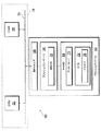
再び図面を参照する。図3は、本発明のコンピュータ・システム60を部分的に示す、高度な概略ブロック図である。図示のアーキテクチャが適当なコンピュータ・システムの例としては、例えばパソコン等のコンピュータ、コンピュータに基づく機器、そして携帯電話等のポータブル機器がある。システム60と従来の技術によるシステム20との両方に共通するコンポーネント(プロセッサ22、RAM26およびバス30)は、同一の参照番号を持つ。システム60とシステム20との間の主要な相違は、システム60において、システム20の三つの不揮発性メモリ・デバイス(BIOS24、ハードディスク28およびフラッシュメモリ・デバイス44)が、単一のフラッシュメモリ・デバイス62で置換されていることである。
Reference is again made to the drawings. FIG. 3 is a high level schematic block diagram partially illustrating the
フラッシュメモリ・デバイス62は、NANDフラッシュメモリ64、フラッシュコントローラ66および実行可能なインターフェイス、特にSRAMインターフェイス68を含む。NANDフラッシュメモリ内には、ブート・コード70と、システム60のオペレーティングシステム72が記憶されている。オペレーティングシステム72は、フラッシュメモリ・デバイス62のためのドライバ76を含む。フラッシュコントローラ48のように、フラッシュコントローラ66は、NANDフラッシュメモリ64のためのフラッシュ管理システムを具現する。フラッシュコントローラ66は、また、電源オンでフラッシュコントローラ66がブート・コード70をコピーする、コピー先のSRAM74を含む。SRAMインターフェイス68が実行可能であることは、システム60がフラッシュメモリ・デバイス62からブートすることを可能にする。これは、あたかも、第二の従来の技術によるアーキテクチャのフラッシュメモリ・デバイスを持つシステムのようである。フラッシュメモリ・デバイス62に対して、システム60の他の部分は、フラッシュメモリ・デバイス62のホスト78である。
The
システム60が起動すると、フラッシュコントローラ66は、ブート・コード70をSRAM74へコピーする。プロセッサ22は、SRAMインターフェイス68を介してSRAM74からブートし、それからRAM26へオペレーティングシステム72をコピーする。システム60上で実行されるオペレーティングシステム72による、そしてアプリケーションによるフラッシュメモリ・デバイス62への、それ以降のアクセスは、ドライバ76を介して行われる。ただし、ブート・コード70を実行した後に、プロセッサ22がオペレーティングシステム72をRAM26へコピーできるためには、ブート・コード70が、ドライバ76をRAM26へコピーするためのインストラクションを含んでいなければならない。そうすれば、以降のオペレーティングシステム72のRAM26へのコピーは、単に、オペレーティングシステム72の残部に関する。
When the
システム60の一つの欠点は、ドライバ76が、SRAMインターフェイス68を介するフラッシュコントローラ66との通信をサポートするよう、最初から書かれていなければならないことである。実行可能なインターフェイスに関連したより複雑な統合化を解決するために、本発明は、ホストと記憶デバイスとの間の実行可能な物理インターフェイス上で、USBインターフェイスまたはSDインターフェイス等の、標準インターフェイス・プロトコルをエミュレートすることが好ましい。そのようなエミュレーションは、ホスト上で実行しているソフトウェア・アプリケーションまたはオペレーティングシステムが、標準インタフェースを物理的に持つデバイスへのアクセスのためにオペレーティングシステムが備える標準ドライバを使用することによって、記憶デバイスに容易にアクセスすることを可能にする。したがって、統合化のすべての努力は、エミュレーション・ソフトウェアへ局所化でき、エミュレーション・ソフトウェアは、記憶デバイス・タイプとホスト・プロセッサ・タイプとのいずれの組み合わせに対しても、僅かに一度だけ仕立てて統合させなければならない。
One drawback of the
図4は、このエミュレーションを行う一つの方法を示す。図4は、本発明のもう一つのコンピュータ・システム80を部分的に示す、高度な概略ブロック図である。システム80は、システム60の改良バージョンであり、システム20、60および/あるいは80に共通するコンポーネントは、同一の参照番号を持つ。システム60および80の相違は、システム80がフラッシュメモリ・デバイス62にアクセスするために使用するドライバ82が、システム20の従来の技術によるドライバ34を改良して書かれていることである。ドライバ82は、上層36を維持しているが、上層36とSRAMインターフェイス68との間の通信を管理するための、本発明の新しい下層84を持つ。
FIG. 4 shows one way of performing this emulation. FIG. 4 is a high level schematic block diagram partially illustrating another computer system 80 of the present invention. System 80 is an improved version of
本発明を限られた数の実施例に関して説明したが、本発明の多くの変形、修正、そして他の応用が可能であることは明らかである。 Although the invention has been described with respect to a limited number of embodiments, it will be appreciated that many variations, modifications and other applications of the invention are possible.
Claims (8)
(b)実行可能なインターフェイス、そして
(c)ホストから前記実行可能なインターフェイスを介して、仮想アドレスで前記NANDフラッシュメモリへアクセスするインストラクションを受信するための、そして前記仮想アドレスを前記NANDフラッシュメモリ内の物理アドレスへ変換するためのコントローラからなる、データ記憶デバイス。 (A) NAND flash memory,
(B) an executable interface; and (c) receiving an instruction to access the NAND flash memory with a virtual address from the host via the executable interface, and storing the virtual address in the NAND flash memory. A data storage device comprising a controller for converting to a physical address.
(b)電源オンで、前記データ記憶デバイスからブートするホストからなる、システム。 A system comprising: (a) the data storage device of claim 2; and (b) a host that boots from the data storage device when powered on.
(a)システム内に、ブート・コードを記憶したNANDフラッシュメモリを含むデータ記憶デバイスを含めるステップ、
(b)電源オンで前記ブート・コードを実行するステップ、
(c)その後、仮想アドレスで前記メモリにアクセスするインストラクションを前記データ記憶デバイスへ出すステップ、そして
(d)前記データ記憶デバイスによって、前記仮想アドレスを前記メモリの物理アドレスへ変換するステップからなる、方法。 A method for operating a system, comprising:
(A) including in the system a data storage device including a NAND flash memory storing boot code;
(B) executing the boot code with power on;
(C) then issuing instructions to the data storage device to access the memory with a virtual address; and (d) converting the virtual address to a physical address of the memory by the data storage device. .
(a)前記ホストへ実行可能なインターフェイスを提示するステップ、
(b)前記ホストから、仮想アドレスで前記メモリにアクセスするインストラクションを受信するステップ、そして
(c)前記仮想アドレスを前記メモリの物理アドレスへ変換するステップからなる、方法。 A data storage device comprising a memory for interacting with a host of said data storage device comprising:
(A) presenting an executable interface to the host;
(B) receiving from the host an instruction to access the memory with a virtual address; and (c) converting the virtual address to a physical address of the memory.
Applications Claiming Priority (3)
| Application Number | Priority Date | Filing Date | Title |
|---|---|---|---|
| US65176205P | 2005-02-11 | 2005-02-11 | |
| US75859906P | 2006-01-13 | 2006-01-13 | |
| PCT/IL2006/000176 WO2006085324A2 (en) | 2005-02-11 | 2006-02-09 | Nand flash memory system architecture |
Related Child Applications (1)
| Application Number | Title | Priority Date | Filing Date |
|---|---|---|---|
| JP2011198168A Division JP2011258236A (en) | 2005-02-11 | 2011-09-12 | Nand flash memory system architecture |
Publications (2)
| Publication Number | Publication Date |
|---|---|
| JP2008530683A true JP2008530683A (en) | 2008-08-07 |
| JP2008530683A5 JP2008530683A5 (en) | 2010-01-07 |
Family
ID=36793445
Family Applications (2)
| Application Number | Title | Priority Date | Filing Date |
|---|---|---|---|
| JP2007554739A Pending JP2008530683A (en) | 2005-02-11 | 2006-02-09 | NAND flash memory system architecture |
| JP2011198168A Pending JP2011258236A (en) | 2005-02-11 | 2011-09-12 | Nand flash memory system architecture |
Family Applications After (1)
| Application Number | Title | Priority Date | Filing Date |
|---|---|---|---|
| JP2011198168A Pending JP2011258236A (en) | 2005-02-11 | 2011-09-12 | Nand flash memory system architecture |
Country Status (6)
| Country | Link |
|---|---|
| US (2) | US8990475B2 (en) |
| EP (1) | EP1851771A2 (en) |
| JP (2) | JP2008530683A (en) |
| KR (1) | KR20080007430A (en) |
| CA (1) | CA2597551A1 (en) |
| WO (1) | WO2006085324A2 (en) |
Cited By (1)
| Publication number | Priority date | Publication date | Assignee | Title |
|---|---|---|---|---|
| JP2011258236A (en) * | 2005-02-11 | 2011-12-22 | Sandisk Il Ltd | Nand flash memory system architecture |
Families Citing this family (24)
| Publication number | Priority date | Publication date | Assignee | Title |
|---|---|---|---|---|
| KR100448905B1 (en) * | 2002-07-29 | 2004-09-16 | 삼성전자주식회사 | Computer system with nand flash memory for booting and storagement |
| KR100634436B1 (en) * | 2004-09-23 | 2006-10-16 | 삼성전자주식회사 | Multi chip system and its boot code fetch method |
| US20070165457A1 (en) * | 2005-09-30 | 2007-07-19 | Jin-Ki Kim | Nonvolatile memory system |
| US7652922B2 (en) | 2005-09-30 | 2010-01-26 | Mosaid Technologies Incorporated | Multiple independent serial link memory |
| WO2007036050A1 (en) | 2005-09-30 | 2007-04-05 | Mosaid Technologies Incorporated | Memory with output control |
| KR100880379B1 (en) * | 2006-05-25 | 2009-01-23 | 삼성전자주식회사 | Information Processing System being boosted by boot code from external |
| US20080005449A1 (en) * | 2006-07-03 | 2008-01-03 | Phison Electronics Corp. | Generalized flash memory and method thereof |
| TWI374361B (en) * | 2007-01-16 | 2012-10-11 | Asustek Comp Inc | Computer and host device thereof and built-in flash memory storage device |
| KR100823171B1 (en) * | 2007-02-01 | 2008-04-18 | 삼성전자주식회사 | Computer system having a partitioned flash translation layer and flash translation layer partition method thereof |
| US8301912B2 (en) * | 2007-12-31 | 2012-10-30 | Sandisk Technologies Inc. | System, method and memory device providing data scrambling compatible with on-chip copy operation |
| US8059455B2 (en) * | 2008-05-09 | 2011-11-15 | Sandisk Il Ltd. | Partial scrambling to reduce correlation |
| US8806293B2 (en) * | 2008-10-09 | 2014-08-12 | Micron Technology, Inc. | Controller to execute error correcting code algorithms and manage NAND memories |
| US9092387B2 (en) | 2008-12-10 | 2015-07-28 | Micron Technology, Inc. | Non-volatile memory device capable of initiating transactions |
| KR101542878B1 (en) * | 2009-02-13 | 2015-08-07 | 삼성전자주식회사 | Nonvolatile memory device having a buffer ram and boot code management method thereof |
| KR20100133710A (en) * | 2009-06-12 | 2010-12-22 | 삼성전자주식회사 | Memory system and code data loading method therof |
| JP2011154547A (en) * | 2010-01-27 | 2011-08-11 | Toshiba Corp | Memory management device and memory management method |
| US8555050B2 (en) | 2010-07-15 | 2013-10-08 | Broadcom Corporation | Apparatus and method thereof for reliable booting from NAND flash memory |
| US20120317377A1 (en) * | 2011-06-09 | 2012-12-13 | Alexander Palay | Dual flash translation layer |
| US20130318284A1 (en) * | 2012-05-24 | 2013-11-28 | Silicon Motion, Inc. | Data Storage Device and Flash Memory Control Method |
| US9053015B2 (en) * | 2013-06-17 | 2015-06-09 | Topcon Positioning Systems, Inc. | NAND flash memory interface controller with GNSS receiver firmware booting capability |
| US9720604B2 (en) | 2015-08-06 | 2017-08-01 | Sandisk Technologies Llc | Block storage protocol to RAM bypass |
| CN107622027A (en) * | 2017-09-20 | 2018-01-23 | 南京扬贺扬微电子科技有限公司 | A kind of All-in-One Flash controllers and fabrication method |
| US11138158B2 (en) | 2019-05-20 | 2021-10-05 | Callplex, Inc. | Binding a local data storage device to remote data storage |
| US11392509B2 (en) * | 2020-08-18 | 2022-07-19 | PetaIO Inc. | Command memory buffer systems and methods |
Citations (5)
| Publication number | Priority date | Publication date | Assignee | Title |
|---|---|---|---|---|
| JP2002278781A (en) * | 2001-03-16 | 2002-09-27 | Tokyo Electron Device Ltd | Storage device, method for controlling storage device and program |
| WO2004049168A1 (en) * | 2002-11-28 | 2004-06-10 | Renesas Technology Corp. | Memory module, memory system, and information device |
| JP2004220557A (en) * | 2003-01-09 | 2004-08-05 | Samsung Electronics Co Ltd | Controller for xip in serial flash memory, its method and flash memory chip using the same |
| JP2004220575A (en) * | 2002-12-27 | 2004-08-05 | Ricoh Co Ltd | Interface circuit of card type memory, asic carrying its circuit and image forming apparatus carrying asic |
| JP2005010942A (en) * | 2003-06-17 | 2005-01-13 | Matsushita Electric Ind Co Ltd | Apparatus with sequential access memory device in which boot code is stored, and method for starting the same |
Family Cites Families (22)
| Publication number | Priority date | Publication date | Assignee | Title |
|---|---|---|---|---|
| US1102814A (en) * | 1912-12-17 | 1914-07-07 | Gabriel Streit | Scythe. |
| US5404485A (en) | 1993-03-08 | 1995-04-04 | M-Systems Flash Disk Pioneers Ltd. | Flash file system |
| US5937425A (en) | 1997-10-16 | 1999-08-10 | M-Systems Flash Disk Pioneers Ltd. | Flash file system optimized for page-mode flash technologies |
| GB9903490D0 (en) * | 1999-02-17 | 1999-04-07 | Memory Corp Plc | Memory system |
| US6567875B1 (en) * | 1999-04-05 | 2003-05-20 | Opti, Inc. | USB data serializer |
| US6148354A (en) | 1999-04-05 | 2000-11-14 | M-Systems Flash Disk Pioneers Ltd. | Architecture for a universal serial bus-based PC flash disk |
| KR100383774B1 (en) * | 2000-01-26 | 2003-05-12 | 삼성전자주식회사 | Memory strcutre for improving bus efficiency of system adopting common interface |
| US6591330B2 (en) | 2001-06-18 | 2003-07-08 | M-Systems Flash Disk Pioneers Ltd. | System and method for flexible flash file |
| US6901499B2 (en) * | 2002-02-27 | 2005-05-31 | Microsoft Corp. | System and method for tracking data stored in a flash memory device |
| US7533214B2 (en) * | 2002-02-27 | 2009-05-12 | Microsoft Corporation | Open architecture flash driver |
| US20030206442A1 (en) * | 2002-05-02 | 2003-11-06 | Jerry Tang | Flash memory bridiging device, method and application system |
| US20040015771A1 (en) * | 2002-07-16 | 2004-01-22 | Menahem Lasser | Error correction for non-volatile memory |
| JP2004133881A (en) * | 2002-08-14 | 2004-04-30 | Ricoh Co Ltd | Interface circuit of card type memory, asic (application specified ic) mounted with its circuit and image forming apparatus mounted with its asic |
| KR100469669B1 (en) * | 2002-09-24 | 2005-02-02 | 삼성전자주식회사 | System to boot using flash memory and the method thereof |
| US7149889B2 (en) * | 2002-12-12 | 2006-12-12 | Scientific-Atlanta, Inc. | Proactive reboot |
| US7266676B2 (en) | 2003-03-21 | 2007-09-04 | Analog Devices, Inc. | Method and apparatus for branch prediction based on branch targets utilizing tag and data arrays |
| US7254690B2 (en) * | 2003-06-02 | 2007-08-07 | S. Aqua Semiconductor Llc | Pipelined semiconductor memories and systems |
| US7752380B2 (en) * | 2003-07-31 | 2010-07-06 | Sandisk Il Ltd | SDRAM memory device with an embedded NAND flash controller |
| US7296143B2 (en) * | 2004-06-22 | 2007-11-13 | Lenovo (Singapore) Pte. Ltd. | Method and system for loading processor boot code from serial flash memory |
| US20060010285A1 (en) * | 2004-07-06 | 2006-01-12 | Prostor Systems, Inc. | Virtual storage for removable storage media |
| US7305539B2 (en) | 2004-10-14 | 2007-12-04 | Sandisk Il Ltd. | Adaptive booting from mass storage device |
| JP2008530683A (en) * | 2005-02-11 | 2008-08-07 | サンディスク アイエル リミテッド | NAND flash memory system architecture |
-
2006
- 2006-02-09 JP JP2007554739A patent/JP2008530683A/en active Pending
- 2006-02-09 WO PCT/IL2006/000176 patent/WO2006085324A2/en active Application Filing
- 2006-02-09 CA CA002597551A patent/CA2597551A1/en not_active Abandoned
- 2006-02-09 EP EP06711158A patent/EP1851771A2/en not_active Withdrawn
- 2006-02-09 KR KR1020077020810A patent/KR20080007430A/en not_active Application Discontinuation
- 2006-02-10 US US11/350,946 patent/US8990475B2/en active Active
-
2007
- 2007-10-25 US US11/923,681 patent/US9063848B2/en active Active
-
2011
- 2011-09-12 JP JP2011198168A patent/JP2011258236A/en active Pending
Patent Citations (5)
| Publication number | Priority date | Publication date | Assignee | Title |
|---|---|---|---|---|
| JP2002278781A (en) * | 2001-03-16 | 2002-09-27 | Tokyo Electron Device Ltd | Storage device, method for controlling storage device and program |
| WO2004049168A1 (en) * | 2002-11-28 | 2004-06-10 | Renesas Technology Corp. | Memory module, memory system, and information device |
| JP2004220575A (en) * | 2002-12-27 | 2004-08-05 | Ricoh Co Ltd | Interface circuit of card type memory, asic carrying its circuit and image forming apparatus carrying asic |
| JP2004220557A (en) * | 2003-01-09 | 2004-08-05 | Samsung Electronics Co Ltd | Controller for xip in serial flash memory, its method and flash memory chip using the same |
| JP2005010942A (en) * | 2003-06-17 | 2005-01-13 | Matsushita Electric Ind Co Ltd | Apparatus with sequential access memory device in which boot code is stored, and method for starting the same |
Cited By (1)
| Publication number | Priority date | Publication date | Assignee | Title |
|---|---|---|---|---|
| JP2011258236A (en) * | 2005-02-11 | 2011-12-22 | Sandisk Il Ltd | Nand flash memory system architecture |
Also Published As
| Publication number | Publication date |
|---|---|
| EP1851771A2 (en) | 2007-11-07 |
| US8990475B2 (en) | 2015-03-24 |
| JP2011258236A (en) | 2011-12-22 |
| CA2597551A1 (en) | 2006-08-17 |
| WO2006085324A3 (en) | 2007-05-03 |
| US20080104311A1 (en) | 2008-05-01 |
| US9063848B2 (en) | 2015-06-23 |
| US20060184724A1 (en) | 2006-08-17 |
| WO2006085324A2 (en) | 2006-08-17 |
| KR20080007430A (en) | 2008-01-21 |
Similar Documents
| Publication | Publication Date | Title |
|---|---|---|
| US9063848B2 (en) | NAND flash memory system architecture | |
| US8296467B2 (en) | Single-chip flash device with boot code transfer capability | |
| KR101395778B1 (en) | Memory card and memory system including the same and operating method thereof | |
| EP1960887B1 (en) | Method for flash-memory management | |
| US7519754B2 (en) | Hard disk drive cache memory and playback device | |
| US8307172B2 (en) | Memory system including memory controller and separately formatted nonvolatile memory to avoid “copy-involving write” during updating file data in the memory | |
| US9152562B2 (en) | Storage sub-system for a computer comprising write-once memory devices and write-many memory devices and related method | |
| US20060064538A1 (en) | Memory controller, memory device and control method for the memory controller | |
| US20150089103A1 (en) | Non-volatile memory controller processing new request before completing current operation, system including same, and method | |
| US20200183677A1 (en) | Boot rom update method and boot-up method of embedded system | |
| US20040143696A1 (en) | Data storage system for fast booting of computer | |
| US8433847B2 (en) | Memory drive that can be operated like optical disk drive and method for virtualizing memory drive as optical disk drive | |
| JP2004295865A (en) | Automatic booting system and automatic booting method | |
| US20130311708A1 (en) | File protecting method and system, and memory controller and memory storage apparatus thereof | |
| CN101142630A (en) | Nand flash memory system architecture | |
| WO2000067132A1 (en) | Combination ata/linear flash memory device | |
| TWI559227B (en) | Computer system having two built-in operating devices that can be dynamically powered on or powered off | |
| KR20060095133A (en) | Method for operating system program stored in non-volatile memory | |
| KR100582403B1 (en) | Embedded System for high-speed booting and its method | |
| KR20060031192A (en) | Embedded system for high-speed booting and its method | |
| US20110082989A1 (en) | Structure and method for making a storage card | |
| US20110125972A1 (en) | Information recording device and information recording method |
Legal Events
| Date | Code | Title | Description |
|---|---|---|---|
| A521 | Written amendment |
Free format text: JAPANESE INTERMEDIATE CODE: A523 Effective date: 20091112 |
|
| A977 | Report on retrieval |
Free format text: JAPANESE INTERMEDIATE CODE: A971007 Effective date: 20110114 |
|
| A131 | Notification of reasons for refusal |
Free format text: JAPANESE INTERMEDIATE CODE: A131 Effective date: 20110121 |
|
| A521 | Written amendment |
Free format text: JAPANESE INTERMEDIATE CODE: A523 Effective date: 20110415 |
|
| A02 | Decision of refusal |
Free format text: JAPANESE INTERMEDIATE CODE: A02 Effective date: 20110513 |
|
| A521 | Written amendment |
Free format text: JAPANESE INTERMEDIATE CODE: A523 Effective date: 20110912 |
|
| A911 | Transfer to examiner for re-examination before appeal (zenchi) |
Free format text: JAPANESE INTERMEDIATE CODE: A911 Effective date: 20110915 |
|
| A912 | Re-examination (zenchi) completed and case transferred to appeal board |
Free format text: JAPANESE INTERMEDIATE CODE: A912 Effective date: 20111216 |
|
| A601 | Written request for extension of time |
Free format text: JAPANESE INTERMEDIATE CODE: A601 Effective date: 20120426 |
|
| A602 | Written permission of extension of time |
Free format text: JAPANESE INTERMEDIATE CODE: A602 Effective date: 20120502 |