JP2008525836A - Control method of lattice spacing in crystal - Google Patents
Control method of lattice spacing in crystal Download PDFInfo
- Publication number
- JP2008525836A JP2008525836A JP2007547656A JP2007547656A JP2008525836A JP 2008525836 A JP2008525836 A JP 2008525836A JP 2007547656 A JP2007547656 A JP 2007547656A JP 2007547656 A JP2007547656 A JP 2007547656A JP 2008525836 A JP2008525836 A JP 2008525836A
- Authority
- JP
- Japan
- Prior art keywords
- particles
- photonic crystal
- electric field
- color filter
- photonic
- Prior art date
- Legal status (The legal status is an assumption and is not a legal conclusion. Google has not performed a legal analysis and makes no representation as to the accuracy of the status listed.)
- Withdrawn
Links
Images


Classifications
-
- B—PERFORMING OPERATIONS; TRANSPORTING
- B82—NANOTECHNOLOGY
- B82Y—SPECIFIC USES OR APPLICATIONS OF NANOSTRUCTURES; MEASUREMENT OR ANALYSIS OF NANOSTRUCTURES; MANUFACTURE OR TREATMENT OF NANOSTRUCTURES
- B82Y20/00—Nanooptics, e.g. quantum optics or photonic crystals
-
- G—PHYSICS
- G02—OPTICS
- G02F—OPTICAL DEVICES OR ARRANGEMENTS FOR THE CONTROL OF LIGHT BY MODIFICATION OF THE OPTICAL PROPERTIES OF THE MEDIA OF THE ELEMENTS INVOLVED THEREIN; NON-LINEAR OPTICS; FREQUENCY-CHANGING OF LIGHT; OPTICAL LOGIC ELEMENTS; OPTICAL ANALOGUE/DIGITAL CONVERTERS
- G02F1/00—Devices or arrangements for the control of the intensity, colour, phase, polarisation or direction of light arriving from an independent light source, e.g. switching, gating or modulating; Non-linear optics
-
- G—PHYSICS
- G02—OPTICS
- G02B—OPTICAL ELEMENTS, SYSTEMS OR APPARATUS
- G02B6/00—Light guides; Structural details of arrangements comprising light guides and other optical elements, e.g. couplings
- G02B6/10—Light guides; Structural details of arrangements comprising light guides and other optical elements, e.g. couplings of the optical waveguide type
- G02B6/12—Light guides; Structural details of arrangements comprising light guides and other optical elements, e.g. couplings of the optical waveguide type of the integrated circuit kind
- G02B6/122—Basic optical elements, e.g. light-guiding paths
- G02B6/1225—Basic optical elements, e.g. light-guiding paths comprising photonic band-gap structures or photonic lattices
-
- G—PHYSICS
- G02—OPTICS
- G02B—OPTICAL ELEMENTS, SYSTEMS OR APPARATUS
- G02B6/00—Light guides; Structural details of arrangements comprising light guides and other optical elements, e.g. couplings
- G02B6/10—Light guides; Structural details of arrangements comprising light guides and other optical elements, e.g. couplings of the optical waveguide type
- G02B6/12—Light guides; Structural details of arrangements comprising light guides and other optical elements, e.g. couplings of the optical waveguide type of the integrated circuit kind
- G02B2006/12166—Manufacturing methods
-
- G—PHYSICS
- G02—OPTICS
- G02F—OPTICAL DEVICES OR ARRANGEMENTS FOR THE CONTROL OF LIGHT BY MODIFICATION OF THE OPTICAL PROPERTIES OF THE MEDIA OF THE ELEMENTS INVOLVED THEREIN; NON-LINEAR OPTICS; FREQUENCY-CHANGING OF LIGHT; OPTICAL LOGIC ELEMENTS; OPTICAL ANALOGUE/DIGITAL CONVERTERS
- G02F2202/00—Materials and properties
- G02F2202/32—Photonic crystals
Abstract
電界を利用することによって、単分散粒子または単分散粒子の混合物の規則的格子の粒子間隔を生成させ、制御する方法である。 This is a method of generating and controlling the regular lattice particle spacing of a monodisperse particle or a mixture of monodisperse particles by using an electric field.
Description
本発明は、結晶分野、特に結晶内の粒子間の格子間隔の制御方法に関する。 The present invention relates to the crystal field, and more particularly to a method for controlling the lattice spacing between particles in a crystal.
先行技術において、フォトニック結晶には光電子工学、レーザ、フラットレンズ、センサ、波長フィルタ、表示装置における幅広い応用範囲があることは良く知られている。フォトニック結晶の一般的な製造方法は、コロイド微粒子のコロイド結晶への自己組織化を利用するものである。この自己組織化工程は、沈降、遠心分離、ろ過、せん断配向または蒸着等、さまざまな方法で実現できる。さらに、電界を使ってコロイドの最密充填アレイを構成できることも周知である。たとえば、(R.C.ヘイワード、D.A.サヴィーユ、I.A.アクセイのElectrophoretic assembly of colloidal crystals with optically turnable micropatterns, Nature, vol 404, p56, 2000)およびその中で引用されている参考文献を参照のこと。これ以外に、AC電圧を2枚の平面電極に印加することによって構成されるコロイド結晶の例がティーイン・ゴン、デイヴィッドT.ウー、デイヴィッドW.M.マーの"Electric Field-Reversible Three-Dimensional Colloidal Crystals", Langmuir, vol 19 p.5967, 2003およびサイモンO.ラムズドン、エリックW.ケイラー、オーリンD.ヴェルヴの"Two-Dimensional Crystallization of Microspheres by a Coplanar AC Electric Field", Langmuir, vol 20, p2108, 2004において紹介されている。 In the prior art, it is well known that photonic crystals have a wide range of applications in optoelectronics, lasers, flat lenses, sensors, wavelength filters, and display devices. A general production method of a photonic crystal utilizes self-assembly of colloidal fine particles into a colloidal crystal. This self-assembly process can be realized by various methods such as sedimentation, centrifugation, filtration, shear orientation or vapor deposition. Furthermore, it is well known that a close packed array of colloids can be constructed using an electric field. For example (RC Hayward, DA Savieille, IA Acey's Electrophoretic assembly of colloidal crystals with optically turnable micropatterns, Nature, vol 404, p56, 2000) and references cited therein. checking ... In addition to this, examples of colloidal crystals formed by applying an AC voltage to two planar electrodes include Tee-Gon, David T. et al. Woo, David W. M.M. Ma's "Electric Field-Reversible Three-Dimensional Colloidal Crystals", Langmuir, vol 19 p.5967, 2003 and Simon O. Ramsdon, Eric W. Kayler, Olin D. Introduced in Verve's "Two-Dimensional Crystallization of Microspheres by a Coplanar AC Electric Field", Langmuir, vol 20, p2108, 2004.
四重極電極構造を使って不均一な電界勾配を発生させ、これを電気泳動による粒子の制御と操作に利用することは周知であり、その最も初期の例のいくつかを説明したものが、H.P.プールの"Dielectrophoresis" Cambridge University Press (1987)である。さらに、「粒子回転」とも呼ばれる回転電界を液体懸濁液中の粒子(多くの場合、細胞等の生物学的粒子)の操作に応用することもよく知られている。たとえば、ジョーンズ,T.B.の"Electromechanics of Particles", (Cambridge University Press, Cambridge, 1995, p83)を参照のこと。特に、四重極電極構造を使って回転電界を印加する方法は、米国特許第6,056,861号に記載されている。 It is well known to use a quadrupole electrode structure to generate a non-uniform electric field gradient that can be used for electrophoretic particle control and manipulation, and some of the earliest examples have been described, H. P. Pool "Dielectrophoresis" is Cambridge University Press (1987). It is also well known to apply a rotating electric field, also called “particle rotation”, to the manipulation of particles in a liquid suspension (in many cases biological particles such as cells). For example, Jones, T.W. B. See "Electromechanics of Particles", (Cambridge University Press, Cambridge, 1995, p83). In particular, a method of applying a rotating electric field using a quadrupole electrode structure is described in US Pat. No. 6,056,861.
しかしながら、上記の先行技術の中に、本明細書で説明するような方法によって、構成されたコロイド結晶の格子間隔を、電界を使って能動的に制御することを提案しているものはない。 However, none of the above prior art proposes to actively control the lattice spacing of a constructed colloidal crystal using an electric field by a method as described herein.
一般に、結晶の格子間隔は、最密充填化された単分散球状粒子の直径によって決定され、いったん結晶構造が形成されると変化しない。 In general, the lattice spacing of a crystal is determined by the diameter of the closest packed monodisperse spherical particles and does not change once the crystal structure is formed.
フォトニック結晶の格子間隔が制御可能であることは有益である。なぜなら、このパラメータが光学ストップバンドの位置を決定し、したがって結晶内の伝播が禁じられるために反射される波長を決定するからである。そこで、フォトニック結晶内の格子間隔を相互作用的に調整できれば、それによって各種の電気光学デバイスの創作が可能となるため、これは好ましい特性である。波長可変フォトニック結晶の作製方法は、米国特許第5,281,370号や、最近では米国特許出願公開20040131799号において開示されている。しかしながら、これらの格子間隔変更方法はどちらも、幾何学的に変形された高分子マトリクスに埋め込まれたフォトニック結晶について実現されるものである。これは、静電界を用いて液体懸濁液中のフォトニック結晶の間隔を相互作用的に制御する本発明とは大きく異なる。フォトニック結晶を高分子マトリクス内に埋め込む方法の限界は、結晶が多結晶としての性質を有する傾向があるという点である。その結果、幅が増大し、強度が低下し、反射されたピークの位置が不確実となる。これらのシステムにおいて格子間隔を調整できる範囲は、高分子マトリクスの柔軟性によって限定され、デバイスが動作できる波長が制限される。さらに、格子間隔を変更できる速度も、高分子マトリクスをどれだけ高速に圧縮または延引できるかに依存する。一般に、0.5から1秒のオーダーの時間が必要であり、高分子マトリクス装置のフォトニック結晶は、光学スイッチやビデオレートアプリケーション用のディスプレイ等、ミリ秒単位もしくはそれ以下の応答時間が要求される各種の電気光学装置には不適当である。 It is beneficial to be able to control the lattice spacing of the photonic crystal. This is because this parameter determines the position of the optical stopband and hence the wavelength that is reflected because propagation within the crystal is prohibited. Thus, if the lattice spacing in the photonic crystal can be adjusted interactively, various electro-optical devices can be created thereby, which is a preferable characteristic. A method for producing a wavelength-tunable photonic crystal is disclosed in US Pat. No. 5,281,370 and recently in US Patent Application Publication No. 20040131799. However, both of these lattice spacing changing methods can be realized for a photonic crystal embedded in a geometrically deformed polymer matrix. This is very different from the present invention in which an electrostatic field is used to interactively control the spacing of the photonic crystals in the liquid suspension. A limitation of the method of embedding a photonic crystal in a polymer matrix is that the crystal tends to have a polycrystal property. As a result, the width increases, the intensity decreases, and the position of the reflected peak is uncertain. The range in which the lattice spacing can be adjusted in these systems is limited by the flexibility of the polymer matrix and limits the wavelengths at which the device can operate. Furthermore, the speed at which the lattice spacing can be changed also depends on how fast the polymer matrix can be compressed or stretched. In general, a time of the order of 0.5 to 1 second is required, and the photonic crystal of the polymer matrix device requires a response time of milliseconds or less, such as an optical switch or a display for video rate application. This is not suitable for various electro-optical devices.
フォトニック結晶を反射型表示装置内の光学フィルタとして用いる利点が、国際公開番号00/77566号および欧州特許第1359459号において提案されている。しかしながら、このような反射型表示装置に本発明を応用することにより、製造しやすさと性能の点でさらに改善することができる。なぜなら、赤、緑、青の画素のための3つの個別のフォトニック結晶フィルタを使うのではなく、波長可変フォトニック結晶を1個使って、高分子に埋め込まれたフォトニック結晶では実現できなかった高速切替速度で、これら3色すべての応答を可能にするからである。
The advantage of using a photonic crystal as an optical filter in a reflective display device has been proposed in
本発明の目的は、先行技術における周知の方法の問題や制約とは無縁の、懸濁液中の粒子の格子間隔を制御する方法を提供することである。 It is an object of the present invention to provide a method for controlling the lattice spacing of particles in a suspension that is independent of the problems and limitations of known methods in the prior art.
本発明は、電界を使って液体懸濁液中のフォトニック結晶の間隔を相互作用的に制御するものである。 The present invention uses an electric field to interactively control the spacing of photonic crystals in a liquid suspension.
本発明によれば、実質的に単分散した粒子または粒子混合物の規則的格子の粒子間隔を制御する方法が提案される。 According to the present invention, a method is proposed for controlling the particle spacing of a regular lattice of substantially monodispersed particles or particle mixtures.
本発明によれば、結晶内の2つの独立した軸に沿った粒子間隔を動的かつ可逆的に制御することが可能となる。粒子は帯電しているため、静電力によって表面が接触しない。しかしながら、粒子は電界によって誘発される一時的双極子によって、六方最密充填(HCP)パターンに保持される。結晶内の粒子間の分離距離は電界によって制御されるため、電界強度を変えることによって格子間隔を変化させることができる。格子間隔の変化は可逆的かつ高速であり、1秒の何分の1かで行われる。 According to the present invention, it is possible to dynamically and reversibly control the particle spacing along two independent axes in a crystal. Since the particles are charged, the surface does not come into contact with the electrostatic force. However, the particles are held in a hexagonal close packed (HCP) pattern by temporary dipoles induced by an electric field. Since the separation distance between particles in the crystal is controlled by an electric field, the lattice spacing can be changed by changing the electric field strength. The change in lattice spacing is reversible and fast, and takes place in a fraction of a second.
本発明により、懸濁液内の粒子の正確、可逆的、動的な位置決めが可能となる。間隔は、高速、可逆的、再現可能な方法で制御できる。本発明はまた、アスペクト比の制御を可能にするため、間隔を軸ごとに変えることができる。 The present invention enables accurate, reversible and dynamic positioning of particles within a suspension. The spacing can be controlled in a fast, reversible and reproducible way. The present invention also allows the spacing to vary from axis to axis to allow control of the aspect ratio.
本発明の特徴と利点は、添付の図面に関連する以下の説明から明確となるであろう。 The features and advantages of the present invention will become apparent from the following description taken in conjunction with the accompanying drawings.
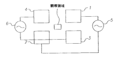
図1は、本発明の方法を説明するために使用される電極のレイアウトを示す。 FIG. 1 shows an electrode layout used to illustrate the method of the present invention.
4個の電極1,2,3,4が観察領域周辺に配置される。電極1,2は信号増幅器5に接続されている。離電極3,4は、信号増幅器6に接続されている。4個の電極は同一平面上にある。実施された実験において、電極1,4と2,3の間の距離は159μmである。電極1,3と2,4の距離は142μmである。しかしながら、ギャップは、必要に応じて調整可能である。距離が短ければ、所望の効果、つまり、30000Vm-1のオーダーの電界強度を得るための電圧が低くてすむ。
Four
電極は、ガラス製の顕微鏡スライド上にスパッタリング被覆した厚さ40nmのプラチナの層である。一般に行われるように、アニオン性ポリスチレンラテックス粒子の希釈懸濁液、10μLアリコートを電極間に流し込み、顕微鏡カバースリップで覆った。各電極のエッジ・エッジ間電気抵抗は100Ω未満、いずれか2個の電極間の抵抗は、懸濁液が存在する状態で5MΩより大きかった。正の位相シフトとは、信号増幅器5が信号増幅器6に先行することを示す。 The electrode is a 40 nm thick layer of platinum sputter coated onto a glass microscope slide. As commonly done, a diluted suspension of anionic polystyrene latex particles, 10 μL aliquots were cast between the electrodes and covered with a microscope cover slip. The electrical resistance between the edges of each electrode was less than 100Ω, and the resistance between any two electrodes was greater than 5 MΩ in the presence of the suspension. A positive phase shift indicates that the signal amplifier 5 precedes the signal amplifier 6.
標準的な手法を使って合成された単分散アニオン性ポリスチレンラテックス粒子のアレイの凝集、運動および粒子間分離距離を観察した。粒子は、Brookhaven Zetaplus光散乱測定器を使って特徴付けられ、その結果、ゼータ電位は0.01mM KClで−40.6mV、平均直径0.93μm(多数分散性0.012)であった。実験は、KCl電解質濃度0.01mMの希釈水性懸濁液(0.29重量%)を使用して行われた。カメラとビデオ録画装置を取り付けた光学顕微鏡を使い、4個の電極の間の中央領域を観察した(図1参照)。図1に詳細に示される4個の同一平面上にある電極1,2,3,4は、2個の信号増幅器5,6に接続され、1600Hzの周波数の正弦波交流電圧を出力する。通常通りに、この配置によって?30,000Vrmsm-1の電界強度が得られ、これによって、粒子は電圧の相対的な大きさと位相に応じて、鎖または回転六方最密充填(HCP)結晶の状態に配列した。観察結果を以下にまとめる。
Aggregation, motion and interparticle separation distance of an array of monodisperse anionic polystyrene latex particles synthesized using standard techniques were observed. The particles were characterized using a Brookhaven Zetasplus light scatterometer, resulting in a zeta potential of −40.6 mV at 0.01 mM KCl and an average diameter of 0.93 μm (polydispersity 0.012). The experiment was performed using a dilute aqueous suspension (0.29 wt%) with a KCl electrolyte concentration of 0.01 mM. Using an optical microscope equipped with a camera and a video recorder, the central region between the four electrodes was observed (see FIG. 1). Four
電界が印加されていないときは、粒子のランダムなブラウン運動がはっきりと見られ、粒子は凝集しなかった。1個の信号増幅器だけが作動すると(電極1と2または3と4)、粒子は自発的に柔軟な鎖状体を形成した。時間の経過とともにより多くの鎖状体が形成されると、隣接する鎖状体は周期的に一緒に漂流し(drifted together)、六方最密充填(HCP)結晶構造を構成した。電界をオフにすると、ブラウン運動によって結晶構造は「分解」した。信号増幅器5だけが動作している状態で形成された鎖状体は、信号増幅器6だけが動作している状態で形成されるものに対して垂直であることが観察された。
When no electric field was applied, the random Brownian motion of the particles was clearly seen and the particles did not aggregate. When only one signal amplifier was activated (
信号増幅器5,6の両方が相対的位相シフト0°で動作している時も鎖状体は形成され、この場合、図1のx軸に平行に配列された。相対的な意味で、この鎖状体は、一方のみの信号増幅器が動作中のときに得られる鎖状体に対して45°回転していた。両方の信号増幅器が相対的位相シフト180°で動作する時には、位相シフトがない場合に得られた鎖状体に垂直な、y軸(図1)に並行に配列した鎖状体が形成された。しかしながら、相対的位相シフトが90°の場合、中間鎖は形成されず、その代わりに、1秒以内にHCP結晶が形成された。これらの結晶は、毎分約50から500回転の速度で回転し、この回転速度は結晶の大きさに反比例する。隣接する結晶は、周期的に漂流し、相互に結合し、結晶の大きさが増す一方で、回転速度は低下した。信号増幅器の片方を切断すると、回転は即座に停止し、結晶の各部分が裂けて鎖状体となった。電極間の中央領域から離れて漂流する結晶も、徐々に裂けて鎖状体になるのが観察された。回転速度は電界強度に比例していた。相対的位相シフトを270°に切り替えると、回転方向が逆転した。1サイクルごとに相対的位相シフトを90°と270°で交互に切り替える、あるいは一方の電圧源の周波数を半分にすることにより、回転する結晶の回転を防止することができる。 Chains were also formed when both signal amplifiers 5, 6 were operating at a relative phase shift of 0 °, in this case arranged parallel to the x-axis of FIG. In a relative sense, this chain was rotated 45 ° with respect to the chain obtained when only one signal amplifier was in operation. When both signal amplifiers operated at a relative phase shift of 180 °, a chain was formed that was aligned parallel to the y-axis (FIG. 1), perpendicular to the chain obtained in the absence of phase shift. . However, when the relative phase shift was 90 °, no intermediate chain was formed, and instead an HCP crystal was formed within 1 second. These crystals rotate at a speed of about 50 to 500 revolutions per minute, which is inversely proportional to the size of the crystals. Adjacent crystals drifted periodically and joined to each other, increasing the size of the crystals while decreasing the rotational speed. When one of the signal amplifiers was cut, the rotation immediately stopped and each part of the crystal was torn into a chain. Crystals drifting away from the central region between the electrodes were also observed to gradually tear into chains. The rotation speed was proportional to the electric field strength. When the relative phase shift was switched to 270 °, the direction of rotation was reversed. By rotating the relative phase shift alternately between 90 ° and 270 ° every cycle, or by halving the frequency of one voltage source, rotation of the rotating crystal can be prevented.
先行技術において、コロイド結晶の可逆的形成は、懸濁液内の粒子に関連する電気的に誘発された双極子の相互作用によって実現できることが知られている。特に、サイモンO.ラムズドン、エリックW.ケイラー、オーリンD.ヴェルヴの"Two-Dimensional Crystallization of Microspheres by a Coplanar AC Electric Field", Langmuir, vol 20, p2108, 2004においては、同一平面上にある電極を使って、低周波数(<20,000Hz)の交流電界(回転しない)を発生させ、これによってラテックス粒子が鎖状体となり、その後2次元平面を形成した。重要な点として、この研究の粒子は、結晶アレイに保持され、その表面の間隔は最大150nmであった。これは、引力と斥力のバランスによって実現された。引力は、電気的に誘発された双極子から発生した。静電斥力は、粒子表面の電荷から発生した。 In the prior art, it is known that reversible formation of colloidal crystals can be achieved by the interaction of electrically induced dipoles associated with particles in suspension. In particular, Simon O. Ramsdon, Eric W. Kayler, Olin D. In Verve's "Two-Dimensional Crystallization of Microspheres by a Coplanar AC Electric Field", Langmuir, vol 20, p2108, 2004, a low frequency (<20,000 Hz) AC electric field (<20,000 Hz) using electrodes on the same plane ( This causes the latex particles to become chain-like and then form a two-dimensional plane. Importantly, the particles in this study were retained in a crystal array with a surface spacing of up to 150 nm. This was achieved by a balance between attractive and repulsive forces. The attraction was generated from an electrically induced dipole. The electrostatic repulsion was generated from the charge on the particle surface.
2つの平行な電極(図1の電極1,4と同様)の間に回転しない交流電界を使用するラムズドン等のものに類似した実験において、電界平行軸に沿った粒子間表面分離距離は、電界垂直軸に沿ったものより常に65%短かった。これを図2に示す。
In an experiment similar to that of Ramsdon et al. Using an alternating electric field that does not rotate between two parallel electrodes (similar to
図2において、すべてのデータポイントは単独の交流電界において測定された粒子間表面分離距離を示す。白いひし形は電界平行軸の粒子分離距離、白丸は電界垂直軸の粒子分離距離である。 In FIG. 2, all data points represent the interparticle surface separation distance measured in a single alternating electric field. The white diamond is the particle separation distance of the electric field parallel axis, and the white circle is the particle separation distance of the electric field vertical axis.
結晶は、鎖状体の間の引力が各鎖状体の中の粒子間の引力よりはるかに小さいため、非対称(細長)であった。これは、隣接する鎖状体の中の双極子の準最適配列と位置決めの制約による。 The crystals were asymmetric (elongated) because the attractive forces between the chains were much less than the attractive forces between the particles in each chain. This is due to sub-optimal arrangement of dipoles in adjacent chains and positioning constraints.
非対称性は、電界を使って制御できることがわかっている。 It has been found that asymmetry can be controlled using an electric field.
本発明においては、同一平面上の四重極電極を使って低周波数(1600Hz)で回転する電界を生成した。しかしながら、100Hzから20kHzまでの範囲の周波数も使用できる。当業者は、電界が回転していることは本発明の本質的要素ではなく、電界のベクトルに時間による変化が生じることが重要であることを理解するであろう。 In the present invention, an electric field rotating at a low frequency (1600 Hz) is generated using a quadrupole electrode on the same plane. However, frequencies in the range from 100 Hz to 20 kHz can also be used. Those skilled in the art will appreciate that the rotation of the electric field is not an essential element of the present invention, but it is important that the vector of the electric field change over time.
実験における結晶の回転は、電界が回転する方向(時計回り、反時計回り)を周期的に切り替えることによって防止された。これによって、2次元結晶構造内の内部間隔を測定することができた。 Crystal rotation in the experiment was prevented by periodically switching the direction in which the electric field rotates (clockwise, counterclockwise). As a result, the internal spacing in the two-dimensional crystal structure could be measured.
1サイクルごとに90°と270°と相対的位相シフトを交互に切り替えることによって結晶の回転を防止した状態で、スチルビデオフレームの画像解析を行った。グラディキュール(gradicule)(Gradicules Ser CS1787,50×2ミクロン)を使って校正した長さ測定の結果、両方の信号増幅器が同じ交流電圧で動作する時、電極1と2の間の対角線軸に沿った粒子間表面分離距離は電極3と4の間の対角線軸に沿ったそれとほぼ等しいことがわかった。信号増幅器5によって伝達された交流電圧の大きさを縮小することによって、電極1と2の間の軸に沿った粒子間分離距離は結晶構造内で34%増大した。これと同時に、電極3と4の間の軸に沿った粒子間分離距離は8%減少した。これを図3に示す。
Still video frame image analysis was performed in a state in which the rotation of the crystal was prevented by alternately switching the relative phase shift between 90 ° and 270 ° for each cycle. As a result of length measurements calibrated using a gradicule (Gradicules Ser CS1787, 50 × 2 microns), along the diagonal axis between
図3において、すべてのデータポイントは回転電界の中で形成された結晶内で測定した粒子間表面分離距離を示す。白丸は電極3と4の間の軸に平行な分離距離を示す(±10°)。×印は電極1と2の間の軸に平行な分離距離を示す(±10°)。実線と破線は、直線回帰フィットである。明確を期すために、電極1と2の間の電界強度を個別に計算したものをx軸に使用した。電極3と4の間の交流電圧の大きさは一定であるため、計算された最大電界成分は38,090Vrmsm-1である(実際の電界強度と方向は、ベクトルの和で計算される)。
In FIG. 3, all data points show the interparticle surface separation distance measured in a crystal formed in a rotating electric field. A white circle indicates a separation distance parallel to the axis between the electrodes 3 and 4 (± 10 °). A cross indicates a separation distance parallel to the axis between the
HCP結晶構造への複合効果として、結晶構造は1つの軸に沿って引き伸ばされた。実験中の流体の流れの存在によってHCP構造がゆがめられ、その結果、立方最密充填(CCP)構造に近いものとなることがわかった。このように格子をゆがめる能力を利用して、フォトニックバンドギャップの大きさを改善できる。 As a combined effect on the HCP crystal structure, the crystal structure was stretched along one axis. It has been found that the presence of fluid flow during the experiment distorts the HCP structure, resulting in a close to cubic close-packed (CCP) structure. Thus, the size of the photonic band gap can be improved by utilizing the ability to distort the lattice.
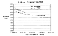
図1に示す実験セットを使い、0.01mM KClに懸濁された760nmポリスチレンラテックス球状粒子(Joel JSM−6330F SEMにより測定)の格子間隔を制御した。ここで、電極は、先端部に高い電界領域が発生しないように、先端を丸くしたものであった。同一平面上の四重極電極系に1000Hzの周波数の回転電界を印加したところ、電界強度は15から35Kvm-1の範囲で変化した。結晶の格子間隔は、2種類の方法で測定した。ひとつ目はin−situでのPS粒子の光学顕微鏡画像による方法、二つ目は2D結晶を通じたダイオードレーザからの635nmの光を照射するとによって得られる第一次回折点の観察と測定による方法である。その結果を図4に示す。 Using the experimental set shown in FIG. 1, the lattice spacing of 760 nm polystyrene latex spherical particles (measured by Joel JSM-6330F SEM) suspended in 0.01 mM KCl was controlled. Here, the electrode has a rounded tip so that a high electric field region does not occur at the tip. When a rotating electric field having a frequency of 1000 Hz was applied to the quadrupole electrode system on the same plane, the electric field strength changed in the range of 15 to 35 Kvm −1 . The crystal lattice spacing was measured by two methods. The first is a method using an optical microscope image of PS particles in-situ, and the second is a method based on observation and measurement of the first diffraction point obtained by irradiating 635 nm light from a diode laser through a 2D crystal. is there. The result is shown in FIG.
図4は、レーザ回折により測定された格子間隔(白い四角)が、光学顕微鏡により測定されたもの(黒い四角)より常に約20nm高いことを示している。しかしながら、どちらの方法で測定された間隔も、電界強度に対して同じ反応を示している。つまり、電界強度が増すと結晶の格子間隔は減少する。 FIG. 4 shows that the grating spacing measured by laser diffraction (white squares) is always about 20 nm higher than that measured by the optical microscope (black squares). However, the spacing measured by either method shows the same response to the electric field strength. That is, as the electric field strength increases, the crystal lattice spacing decreases.
下表は、図4に示す装置に白色光を〜30から50度で照射したときの視認可能な色の観察結果を示す。この実験において、電界強度は35Kvm-1で変わらないが、電界の方向と位相は異なる。 The table below shows the observation results of visible colors when the device shown in FIG. 4 is irradiated with white light at ˜30 to 50 degrees. In this experiment, the electric field strength does not change at 35 Kvm −1 , but the electric field direction and phase are different.

上記の実験では、電界におけるコロイド結晶の高速な組織化が実証された。さらに、これらの実験によって、結晶の回転の制御および独立した軸に沿った格子間隔に対する動的かつ高速かつ可逆的な制御が可能であることも証明された。フォトニック結晶の格子間隔を相互作用的に調整できることは、光電子機器において、波長可変フィルタ素子、あるいは調整可能な光学特性を有するフラットレンズにとって、またディスプレイ内の波長可変色素子の部品として、あるいはCCD,CMOSまたはフィルムカメラやサーマルイメージャ等のその他の画像撮影装置用の波長可変光学フィルタとして使用可能なディスプレイ業界において特に有益である。そのほか、赤、緑、青のフィールドが連続的に撮影もしくは表示される、フィールドシーケンシャルモードでの撮影もしくは表示を利用するアプローチもある。 The above experiments demonstrated fast organization of colloidal crystals in an electric field. In addition, these experiments have also demonstrated that control of crystal rotation and dynamic, fast and reversible control of lattice spacing along independent axes is possible. The ability to interactively adjust the lattice spacing of photonic crystals can be used in optoelectronics, for tunable filter elements, flat lenses with adjustable optical properties, as components of tunable color elements in displays, or as CCD , Especially useful in the display industry that can be used as a tunable optical filter for CMOS or other imaging devices such as film cameras and thermal imagers. In addition, there is an approach using shooting or display in a field sequential mode in which red, green, and blue fields are continuously shot or displayed.
コロイド粒子の大きさを適当に選択することによって、このデバイスを電磁スペクトルの異なる領域を制御するために使用できる。たとえば、100から600nmの範囲の大きさの粒子は、スペクトルの可視領域において動作するデバイスに使用され、マイクロメートルの範囲の大きさの粒子は、スペクトルの赤外線領域でデバイスを動作させるのに使用される。さらに大きな粒子の使用により、スペクトルのテラヘルツおよびマイクロ波領域における動作が可能となる。 By appropriately selecting the size of the colloidal particles, this device can be used to control different regions of the electromagnetic spectrum. For example, particles with a size in the range of 100 to 600 nm are used for devices operating in the visible region of the spectrum, and particles with a size in the micrometer range are used to operate the device in the infrared region of the spectrum. The The use of larger particles allows operation in the terahertz and microwave regions of the spectrum.
ポリスチレンまたはシリカの単分散球状粒子の使用に加え、機能性球状粒子も利用でき、あるいはセラミック、金属酸化物もしくは金属塩、高分子または金属層等、異なるひとつまたは複数の材料のシェルあるいは金属の層を有するコア粒子を含む球状粒子を使って表面プラズモンを操作し、またはフォトニックバンドギャップを改善できる。さらに、中空の粒子もしくは気泡を使い、懸濁する液体と粒子の間の誘電コントラストをより大きくすることが可能である。中空の粒子により、構成された格子はシェルの内側と外側で異なる長さスケールを持ち、これを利用してバンドギャップを改善できる。さらに高度なものとするためには、複数の、制御可能な長さスケールを持たせるために、異なる誘電率を有する材料からなる複数の交互に重ねられた層を持つ中空の粒子を使用する。バンドギャップを大きくするための別の方法として、2つの異なる大きさの単分散球状粒子を使って、大きさごとの量の比率を調整し、最終的な格子の充填構造を変更してもよい。この方法のバリエーションとして、アスペクト比が1より大きい楕円、棒状または板状の粒子等の非対称粒子を使い、充填対称性を変化させる方法がある。このような形状の異なる粒子は、個別にも、組み合わせても使用できる。さらに、たとえば液体または高分子の単分散液滴を有する限定的合体乳濁液を使用することも可能であり、この液滴は液滴表面に結合させた粒子によって安定化され、このようにして、表面電荷を発生させる安定化粒子を使って液滴が表面電荷を帯びるようにすることができる。液滴を電界の印加によってその誘電特性を変化させる液晶材料とするか、あるいは液滴にこうした液晶材料を含めることにより、フォトニック結晶の光学応答を選択的に調整する、また別の機会を得ることができる。 In addition to the use of monodispersed spherical particles of polystyrene or silica, functional spherical particles can also be used, or shells or layers of metal of one or more different materials such as ceramics, metal oxides or metal salts, polymers or metal layers Spherical particles containing core particles with can be used to manipulate surface plasmons or improve photonic band gap. Furthermore, it is possible to use a hollow particle or bubble to increase the dielectric contrast between the suspended liquid and the particle. With hollow particles, the constructed lattice has different length scales on the inside and outside of the shell, which can be used to improve the band gap. To be more sophisticated, hollow particles with a plurality of alternating layers of materials having different dielectric constants are used to have a plurality of controllable length scales. Another way to increase the bandgap is to use two differently sized monodisperse spherical particles to adjust the ratio of the quantity per size and change the final lattice packing structure . As a variation of this method, there is a method of changing the filling symmetry by using asymmetrical particles such as elliptical, rod-like or plate-like particles having an aspect ratio larger than 1. Such particles having different shapes can be used individually or in combination. Furthermore, it is also possible to use limited coalescence emulsions with, for example, liquid or polymer monodisperse droplets, which are stabilized by particles bound to the surface of the droplets, thus The stabilizing particles that generate surface charge can be used to cause the droplet to carry surface charge. Another opportunity is to selectively tune the optical response of the photonic crystal by making the droplet a liquid crystal material that changes its dielectric properties by applying an electric field, or by including such a liquid crystal material in the droplet. be able to.
例として紹介した粒子は、その表面に一定の電荷を有し、これが斥力を発生させて粒子を分離した状態に保つ。この力は、電界によって発生される双極子の引力と平衡が保たれる。しかしながら、最小限の要求事項は粒子が相互反発することであり、これは、表面活性剤またはオリゴマもしくは高分子等の1層または複数の吸収層や、たとえば粒子表面上の帯電粒子その他の分散剤の層による立体反発を利用する等、その他の手段でも実現でき、これによって永久的に表面電荷を持たせることに対する要求が緩和される。 The particles introduced as an example have a constant charge on their surface, which generates repulsive forces and keeps the particles separated. This force is balanced with the dipole attraction generated by the electric field. However, the minimum requirement is that the particles repel each other, which may be one or more absorbent layers such as surfactants or oligomers or polymers, or charged particles or other dispersants on the particle surface, for example. Other means such as the use of steric repulsion by the layer can be realized, which alleviates the requirement for having a surface charge permanently.
本発明を好ましい実施形態に関連して説明した。当業者は、本発明の範囲内で変更や改変が可能であると理解できるであろう。 The invention has been described with reference to the preferred embodiments. Those skilled in the art will appreciate that changes and modifications can be made within the scope of the present invention.
Claims (32)
前記粒子の格子はフォトニック結晶を形成することを特徴とする方法。 The method of claim 1, comprising:
A method characterized in that the lattice of particles forms a photonic crystal.
前記格子は、電界によって生成されることを特徴とする方法。 The method according to claim 1 or 2, comprising:
The method wherein the grid is generated by an electric field.
2個またはそれ以上のペアの電極によって電圧が供給され、電極の各ペアは独立した電圧源に接続され、前記電圧源の相対的位相が制御されることを特徴とする方法。 A method according to any one of claims 1, 2 or 3, comprising
A method in which a voltage is supplied by two or more pairs of electrodes, each pair of electrodes being connected to an independent voltage source, and the relative phase of the voltage source is controlled.
前記印加された電界の周波数は、100Hzと20kHzの間であることを特徴とする方法。 A method according to any one of claims 1 to 4, comprising
The method, wherein the frequency of the applied electric field is between 100 Hz and 20 kHz.
前記印加された電界の周波数は、1000Hzと10kHzの間であることを特徴とする方法。 6. A method according to claim 5, wherein
The method, wherein the frequency of the applied electric field is between 1000 Hz and 10 kHz.
前記粒子の大きさは100nmから600nmの範囲であることを特徴とする方法。 A method according to any one of claims 1 to 6, comprising
The method according to claim 1, wherein the size of the particles is in the range of 100 nm to 600 nm.
前記粒子の大きさは600nmから1000μmの範囲であることを特徴とする方法。 A method according to any one of claims 1 to 6, comprising
The method according to claim 1, wherein the size of the particles is in the range of 600 nm to 1000 μm.
前記粒子の大きさは1mmから10mmの範囲であることを特徴とする方法。 A method according to any one of claims 1 to 6, comprising
The method according to claim 1, wherein the size of the particles is in the range of 1 mm to 10 mm.
前記粒子は、少なくとも±10mVゼータ電位あるいは、より好ましくは±40mVまたはそれを超える表面電荷を有し、粒子が相互に反発することを特徴とする方法。 A method according to any one of claims 1 to 9, comprising:
The method wherein the particles have a surface charge of at least ± 10 mV zeta potential, or more preferably ± 40 mV or more, and the particles repel each other.
前記粒子は、表面活性剤またはオリゴマもしくは高分子からなる、あるいはより小さな帯電粒子の1層または複数の層を有し、粒子間の立体反発を創出し、粒子を相互に反発させることを特徴とする方法。 A method according to any one of claims 1 to 9, comprising:
The particles are composed of a surfactant, an oligomer or a polymer, or have one or more layers of smaller charged particles, creating steric repulsion between the particles and repelling each other. how to.
前記電界の強度は5000から100000Vm-1の範囲であることを特徴とする方法。 12. A method according to any one of claims 1 to 11, comprising:
The method, wherein the electric field strength is in the range of 5000 to 100,000 Vm −1 .
前記電界の強度は1000から80000Vm-1の範囲であることを特徴とする方法。 The method of claim 12, comprising:
The method, wherein the electric field strength is in the range of 1000 to 80000 Vm- 1 .
前記結晶格子構造は、異なる軸に沿って異なる大きさの力を加えることにより、六方最密充填もしくは面心立方から立方最密充填構造に体系的に移行され、フォトニックバンドギャップが改善されることを特徴とする方法。 14. A method according to any one of claims 1 to 13, comprising
The crystal lattice structure is systematically shifted from a hexagonal close-packed or face-centered cubic to a cubic close-packed structure by applying forces of different magnitudes along different axes, improving the photonic band gap. A method characterized by that.
前記結晶格子の対称性は、楕円、棒状または板状の粒子あるいはその他の非球状粒子等、アスペクト比の高い粒子を含めることによって体系的にシフトされることを特徴とする方法。 14. A method according to any one of claims 1 to 13, comprising
A method characterized in that the symmetry of the crystal lattice is systematically shifted by including particles with a high aspect ratio, such as elliptical, rod-like or plate-like particles or other non-spherical particles.
前記結晶格子の対称性は、より小さな粒子の大きさを適当に選択することによってより大きな粒子の格子の対称性を変化させることができるように、大きさの比率が調整される、2つまたはそれ以上の粒子サイズを混合させて使用することによって体系的にシフトされることを特徴とする方法。 14. A method according to any one of claims 1 to 13, comprising
The symmetry of the crystal lattice is such that the ratio of the sizes is adjusted so that the symmetry of the lattice of the larger particles can be changed by appropriately selecting the size of the smaller particles, or A method characterized in that it is systematically shifted by using a mixture of larger particle sizes.
前記格子の組立に使用される前記粒子が中空であることを特徴とする方法。 A method according to any one of claims 1 to 16, comprising:
A method wherein the particles used in the assembly of the lattice are hollow.
前記格子の組立に使用される前記粒子が中空であり、金属もしくは誘電材料あるいは金属と誘電材料の組み合わせによる複数の層を備えることを特徴とする方法。 A method according to any one of claims 1 to 17, comprising
The method wherein the particles used in the assembly of the lattice are hollow and comprise a plurality of layers of metal or dielectric material or a combination of metal and dielectric material.
前記フォトニック結晶の組立に使用される粒子は、高分子、有機、無機、セラミック、金属、金属酸化物または金属塩あるいは金属被覆粒子であることを特徴とする方法。 19. A method according to any one of claims 2 to 18, comprising
The particle used for the assembly of the photonic crystal is a polymer, organic, inorganic, ceramic, metal, metal oxide or metal salt or metal-coated particle.
使用される前記粒子は、界面部分で帯電粒子を吸収することによって安定化された限定的合体乳濁液の単分散液滴であることを特徴とする方法。 A method according to any one of claims 1 to 19, comprising
The method is characterized in that the particles used are monodisperse droplets of a limited coalescence emulsion stabilized by absorbing charged particles at the interface.
前記液滴は、光学応答性をさらに調整するために、液晶材料からなる、あるいはこれを含むことを特徴とする方法。 The method of claim 20, comprising:
The droplet is made of or includes a liquid crystal material to further adjust the optical response.
前記粒子は、光学応答性をさらに調整するために、液晶材料中に懸濁されることを特徴とする方法。 A method according to any one of claims 1 to 20, comprising
The method wherein the particles are suspended in a liquid crystal material to further adjust optical response.
懸濁液中の結晶内の格子間隔が、懸濁液に電界を印加することによって制御されることを特徴とする製造方法。 A method of manufacturing a wavelength tunable colloid photonic crystal device, comprising:
A manufacturing method, wherein a lattice spacing in a crystal in a suspension is controlled by applying an electric field to the suspension.
格子の寸法が請求項1に記載の方法によって制御されることを特徴とするフォトニック結晶装置。 A photonic crystal device using a suspension having reversibly adjustable photonic properties,
A photonic crystal device, wherein the dimensions of the lattice are controlled by the method of claim 1.
格子の寸法は、請求項1に記載の方法によって制御され、反射型または透過型ディスプレイの部品として、特定の波長の光を選択的に反射もしくは透過するために使用できることを特徴とするフォトニック結晶カラーフィルタ装置。 A photonic crystal color filter device using a suspension having reversibly adjustable photonic properties,
The size of the grating is controlled by the method of claim 1 and can be used as a part of a reflective or transmissive display to selectively reflect or transmit light of a specific wavelength. Color filter device.
前記装置は粒子の鎖状体を含み、この鎖状体は前記鎖状体の角度方向によって決定される周期の回折格子を形成し、請求項1に記載の方法によって制御され、反射型もしくは透過型ディスプレイの部品として、特定の波長の光を選択的に反射もしくは透過するために使用されることを特徴とするフォトニック結晶カラーフィルタ装置。 A photonic crystal color filter device using a suspension having reversibly adjustable photonic properties,
The apparatus comprises a chain of particles, the chain forming a diffraction grating with a period determined by the angular direction of the chain, controlled by the method of claim 1, reflective or transmissive. A photonic crystal color filter device, which is used for selectively reflecting or transmitting light of a specific wavelength as a part of a mold display.
格子の寸法は請求項1に記載の方法によって制御され、CMOSまたはCCDあるいはその他の画像撮影素子のフィルタアレイの一部として、特定の波長の光を選択的に反射もしくは透過するために使用されることを特徴とするフォトニック結晶カラーフィルタ装置。 A photonic crystal color filter device using a suspension having reversibly adjustable photonic properties,
The size of the grating is controlled by the method of claim 1 and used to selectively reflect or transmit light of a specific wavelength as part of a filter array of CMOS or CCD or other imaging elements. A photonic crystal color filter device.
前記装置は粒子の鎖状体を含み、この鎖状体は前記鎖状体の角度方向によって決定される周期の回折格子を形成し、請求項1に記載の方法によって制御され、CMOSまたはCCDあるいはその他の画像撮影素子上のフィルタアレイの一部として、特定の波長の光を選択的に反射もしくは透過するために使用されることを特徴とするフォトニック結晶カラーフィルタ装置。 There is a photonic crystal color filter device using a suspension having reversibly adjustable photonic properties,
The apparatus includes a chain of particles, which form a diffraction grating with a period determined by the angular direction of the chain, controlled by the method of claim 1, and can be a CMOS or CCD or A photonic crystal color filter device, which is used for selectively reflecting or transmitting light of a specific wavelength as a part of a filter array on another image photographing element.
格子の寸法は請求項1に記載の方法によって制御され、フィールドシーケンシャルモードで動作する画像撮影もしくは表示装置の部品として、特定の波長の光を選択的に反射もしくは透過するために使用されることを特徴とするフォトニック結晶カラーフィルタ装置。 A photonic crystal color filter device using a suspension having reversibly adjustable photonic properties,
The size of the grating is controlled by the method of claim 1 and is used as a part of an imaging or display device operating in field sequential mode to selectively reflect or transmit light of a specific wavelength. A photonic crystal color filter device.
前記装置は粒子の鎖状体を含み、この鎖状体は前記鎖状体の角度方向によって決定される周期の回折格子を形成し、請求項1に記載の方法によって制御され、フィールドシーケンシャルモードで動作可能な画像撮影もしくは表示装置の部品として、特定の波長の光を選択的に反射もしくは透過するために使用されることを特徴とするフォトニック結晶カラーフィルタ装置。 A photonic crystal color filter device using a suspension having reversibly adjustable photonic properties,
The apparatus comprises a chain of particles, the chain forming a diffraction grating with a period determined by the angular orientation of the chain, controlled by the method of claim 1 and in field sequential mode. A photonic crystal color filter device that is used to selectively reflect or transmit light of a specific wavelength as a component of an operable image capturing or display device.
前記格子の寸法は、調整可能な負屈折率を有するフラットレンズ装置を作製するための材料を使って請求項1に記載の方法によって制御されることを特徴とするフォトニック結晶装置。 A photonic crystal device using a suspension having reversibly adjustable photonic properties,
The photonic crystal device according to claim 1, wherein the size of the grating is controlled by the method of claim 1 using a material for making a flat lens device having an adjustable negative refractive index.
Applications Claiming Priority (2)
| Application Number | Priority Date | Filing Date | Title |
|---|---|---|---|
| GBGB0428261.2A GB0428261D0 (en) | 2004-12-23 | 2004-12-23 | Control of lattice spacing within crystals |
| PCT/GB2005/005029 WO2006067482A2 (en) | 2004-12-23 | 2005-12-22 | Control of lattice spacing within crystals |
Publications (2)
| Publication Number | Publication Date |
|---|---|
| JP2008525836A true JP2008525836A (en) | 2008-07-17 |
| JP2008525836A5 JP2008525836A5 (en) | 2008-12-25 |
Family
ID=34113188
Family Applications (1)
| Application Number | Title | Priority Date | Filing Date |
|---|---|---|---|
| JP2007547656A Withdrawn JP2008525836A (en) | 2004-12-23 | 2005-12-22 | Control method of lattice spacing in crystal |
Country Status (6)
| Country | Link |
|---|---|
| US (1) | US20080230752A1 (en) |
| EP (1) | EP1828823A2 (en) |
| JP (1) | JP2008525836A (en) |
| CN (1) | CN101084459A (en) |
| GB (1) | GB0428261D0 (en) |
| WO (1) | WO2006067482A2 (en) |
Cited By (5)
| Publication number | Priority date | Publication date | Assignee | Title |
|---|---|---|---|---|
| KR20110050930A (en) * | 2009-11-09 | 2011-05-17 | 삼성전자주식회사 | Method for manufacturing a reflective color filter |
| JP2013501257A (en) * | 2009-08-05 | 2013-01-10 | ナノブリック カンパニー リミテッド | Printing medium, printing method and printing apparatus using photocrystallinity |
| JP2013538365A (en) * | 2010-07-19 | 2013-10-10 | ナノブリック カンパニー リミテッド | Display device, display method, and computer-readable recording medium |
| JP2013539058A (en) * | 2010-06-29 | 2013-10-17 | ナノブリック カンパニー リミテッド | Surface display method and apparatus |
| JP2014534459A (en) * | 2011-10-10 | 2014-12-18 | ラムダ ガード テクノロジーズ リミテッド | Filters created with metamaterials |
Families Citing this family (17)
| Publication number | Priority date | Publication date | Assignee | Title |
|---|---|---|---|---|
| JP2008026346A (en) * | 2006-07-18 | 2008-02-07 | Hokkaido Univ | Color filter for transmissive display using photonic crystal |
| GB0722131D0 (en) * | 2007-11-10 | 2007-12-19 | Eastman Kodak Co | Control of lattice spacing within crystals |
| KR20090086192A (en) * | 2009-07-22 | 2009-08-11 | 주식회사 나노브릭 | Display method and device using photonic crystal characteristics |
| EP2488841A2 (en) | 2009-10-16 | 2012-08-22 | Koninklijke Philips Electronics N.V. | A spectral detection device for detecting spectral components of received light |
| US20110135888A1 (en) * | 2009-12-04 | 2011-06-09 | Ppg Industries Ohio, Inc. | Crystalline colloidal array of particles bearing reactive surfactant |
| US8477402B2 (en) | 2010-09-20 | 2013-07-02 | The Invention Science Fund I Llc | Photonic modulation of a photonic band gap |
| US9561615B2 (en) | 2011-01-12 | 2017-02-07 | Cambridge Enterprise Limited | Manufacture of composite optical materials |
| GB201105663D0 (en) | 2011-04-01 | 2011-05-18 | Cambridge Entpr Ltd | Structural colour materials and methods for their manufacture |
| US9074090B2 (en) | 2011-04-15 | 2015-07-07 | GM Global Technology Operations LLC | Shape memory polymer-based tunable photonic device |
| KR101942966B1 (en) | 2011-08-18 | 2019-01-29 | 삼성전자주식회사 | Method of preparing mono disperse particle, mono disperse particle prepared by using the method, and tunable photonic crystal device using the mono disperse particle |
| KR101968634B1 (en) | 2011-08-24 | 2019-04-15 | 삼성전자주식회사 | Method of preparing high refractive nano particle, nano particle prepared by using the method, and photonic crystal device using the nano particle |
| DE102011111980A1 (en) * | 2011-08-29 | 2013-02-28 | Osram Opto Semiconductors Gmbh | Method for producing a light-emitting diode and light-emitting diode |
| CN103436965B (en) * | 2013-07-13 | 2016-03-16 | 吉林大学 | Forbidden photon band is adjustable and present the preparation method of polymer photon crystal of patterning color display |
| US9733467B2 (en) * | 2014-12-03 | 2017-08-15 | Hyundai Motor Company | Smart glass using guided self-assembled photonic crystal |
| US9874693B2 (en) | 2015-06-10 | 2018-01-23 | The Research Foundation For The State University Of New York | Method and structure for integrating photonics with CMOs |
| CN109061936A (en) | 2018-10-26 | 2018-12-21 | 合肥鑫晟光电科技有限公司 | Dot structure, display panel and its manufacture and control method, display device |
| CN113433727B (en) * | 2021-06-18 | 2023-04-07 | 珠海光驭科技有限公司 | Electrochromic optical film and preparation method thereof |
Family Cites Families (7)
| Publication number | Priority date | Publication date | Assignee | Title |
|---|---|---|---|---|
| US4632517A (en) * | 1983-12-08 | 1986-12-30 | University Of Pittsburgh | Crystalline colloidal narrow band radiation filter |
| US6721083B2 (en) * | 1996-07-19 | 2004-04-13 | E Ink Corporation | Electrophoretic displays using nanoparticles |
| US7226966B2 (en) * | 2001-08-03 | 2007-06-05 | Nanogram Corporation | Structures incorporating polymer-inorganic particle blends |
| DE10001172A1 (en) * | 2000-01-13 | 2001-07-26 | Max Planck Gesellschaft | Templating solid particles with polymer multilayers |
| US6533903B2 (en) * | 2000-04-28 | 2003-03-18 | Princeton University | Electrohydrodynamically patterned colloidal crystals |
| WO2002091028A2 (en) * | 2001-05-03 | 2002-11-14 | Colorado School Of Mines | Devices employing colloidal-sized particles |
| WO2004059347A2 (en) * | 2002-12-20 | 2004-07-15 | Minerva Biotechnologies Corporation | Optical devices and methods involving nanoparticles |
-
2004
- 2004-12-23 GB GBGB0428261.2A patent/GB0428261D0/en not_active Ceased
-
2005
- 2005-12-22 CN CNA2005800439450A patent/CN101084459A/en active Pending
- 2005-12-22 WO PCT/GB2005/005029 patent/WO2006067482A2/en active Application Filing
- 2005-12-22 US US11/813,487 patent/US20080230752A1/en not_active Abandoned
- 2005-12-22 EP EP05843717A patent/EP1828823A2/en not_active Withdrawn
- 2005-12-22 JP JP2007547656A patent/JP2008525836A/en not_active Withdrawn
Cited By (10)
| Publication number | Priority date | Publication date | Assignee | Title |
|---|---|---|---|---|
| JP2013501257A (en) * | 2009-08-05 | 2013-01-10 | ナノブリック カンパニー リミテッド | Printing medium, printing method and printing apparatus using photocrystallinity |
| KR20110050930A (en) * | 2009-11-09 | 2011-05-17 | 삼성전자주식회사 | Method for manufacturing a reflective color filter |
| KR101631983B1 (en) | 2009-11-09 | 2016-06-21 | 삼성전자주식회사 | Method for manufacturing a reflective color filter |
| JP2013539058A (en) * | 2010-06-29 | 2013-10-17 | ナノブリック カンパニー リミテッド | Surface display method and apparatus |
| JP2016197256A (en) * | 2010-06-29 | 2016-11-24 | ナノブリック カンパニー リミテッド | Surface display method and device |
| US9625784B2 (en) | 2010-06-29 | 2017-04-18 | Nanobrick Co., Ltd. | Method for tuning color of a display region and apparatus thereof |
| JP2013538365A (en) * | 2010-07-19 | 2013-10-10 | ナノブリック カンパニー リミテッド | Display device, display method, and computer-readable recording medium |
| JP2014534459A (en) * | 2011-10-10 | 2014-12-18 | ラムダ ガード テクノロジーズ リミテッド | Filters created with metamaterials |
| US10698143B2 (en) | 2011-10-10 | 2020-06-30 | Lamda Guard Technologies Ltd. | Filter made of metamaterials |
| US10996385B2 (en) | 2011-10-10 | 2021-05-04 | Lamda Guard Technologies Ltd. | Filter made of metamaterials |
Also Published As
| Publication number | Publication date |
|---|---|
| US20080230752A1 (en) | 2008-09-25 |
| EP1828823A2 (en) | 2007-09-05 |
| CN101084459A (en) | 2007-12-05 |
| GB0428261D0 (en) | 2005-01-26 |
| WO2006067482A2 (en) | 2006-06-29 |
| WO2006067482A3 (en) | 2006-09-08 |
Similar Documents
| Publication | Publication Date | Title |
|---|---|---|
| JP2008525836A (en) | Control method of lattice spacing in crystal | |
| Dinsmore et al. | Self-assembly of colloidal crystals | |
| EP1387209B1 (en) | Light regulating device and photonic crystal display utilizing photonic bandgap controls | |
| JP6849597B2 (en) | Light modulation element including gate structure | |
| JP6754963B2 (en) | Colloidal eutectic, colloidal eutectic solidified product, and method for producing them | |
| US9632216B2 (en) | Optical modulating device having gate structure | |
| Yethiraj | Tunable colloids: control of colloidal phase transitions with tunable interactions | |
| KR101704983B1 (en) | Multi-color electro-optic displays | |
| EP1212477B1 (en) | Colloidal photonic crystals | |
| EP2847635B1 (en) | Three dimensional display system based on fluorescence emission of nanorods | |
| CN105190417B (en) | Phase-modulator | |
| US11112546B2 (en) | Method for preparing coating layer having highly aligned nanomaterial in lyotropic liquid crystal matrix | |
| KR20070041714A (en) | Light modulator | |
| JP2001516467A (en) | Improved microencapsulated electrophoretic display | |
| KR101313812B1 (en) | Method of fabrication of liquid film, method of arranging nano paticles and substrate to have liquid thin film manufactured by using the same | |
| JP2011514555A (en) | Electrophoretic display device | |
| CN1260904A (en) | Ordered structure in homogeneous magnetic fluid thin films and method of preparation | |
| JP3978236B2 (en) | Magnetic fluid thin film display and monochromatic optical switch and tunable wavelength filter | |
| JP2010503032A (en) | Active optical element and manufacturing method thereof | |
| US20220213613A1 (en) | Colloidal crystal having diamond lattice structure and method for producing same | |
| US7295364B2 (en) | Colorant, particles for display device, image display medium and image forming apparatus | |
| Wang et al. | Effect of anionic surfactants on synthesis and self-assembly of silica colloidal nanoparticles | |
| Fan et al. | Transmittance tuning by particle chain polarization in electrowetting-driven droplets | |
| CN105204193B (en) | Control the display device and its manufacturing method of angles of display | |
| WO2009060166A1 (en) | Control of lattice spacing within photonic crystals |
Legal Events
| Date | Code | Title | Description |
|---|---|---|---|
| A521 | Request for written amendment filed |
Free format text: JAPANESE INTERMEDIATE CODE: A523 Effective date: 20081104 |
|
| A621 | Written request for application examination |
Free format text: JAPANESE INTERMEDIATE CODE: A621 Effective date: 20081104 |
|
| A761 | Written withdrawal of application |
Free format text: JAPANESE INTERMEDIATE CODE: A761 Effective date: 20090626 |