JP2008513977A - Unidirectional diffusion of metal silicide in semiconductor devices. - Google Patents
Unidirectional diffusion of metal silicide in semiconductor devices. Download PDFInfo
- Publication number
- JP2008513977A JP2008513977A JP2007530694A JP2007530694A JP2008513977A JP 2008513977 A JP2008513977 A JP 2008513977A JP 2007530694 A JP2007530694 A JP 2007530694A JP 2007530694 A JP2007530694 A JP 2007530694A JP 2008513977 A JP2008513977 A JP 2008513977A
- Authority
- JP
- Japan
- Prior art keywords
- metal
- silicide
- temperature
- alloy layer
- layer
- Prior art date
- Legal status (The legal status is an assumption and is not a legal conclusion. Google has not performed a legal analysis and makes no representation as to the accuracy of the status listed.)
- Withdrawn
Links
- 239000002184 metal Substances 0.000 title claims abstract description 149
- 229910052751 metal Inorganic materials 0.000 title claims abstract description 149
- 229910021332 silicide Inorganic materials 0.000 title claims abstract description 127
- FVBUAEGBCNSCDD-UHFFFAOYSA-N silicide(4-) Chemical compound [Si-4] FVBUAEGBCNSCDD-UHFFFAOYSA-N 0.000 title claims abstract description 126
- 238000009792 diffusion process Methods 0.000 title claims abstract description 31
- 239000004065 semiconductor Substances 0.000 title claims abstract description 12
- 238000000034 method Methods 0.000 claims abstract description 100
- 229910000676 Si alloy Inorganic materials 0.000 claims abstract description 40
- 229910045601 alloy Inorganic materials 0.000 claims abstract description 22
- 239000000956 alloy Substances 0.000 claims abstract description 22
- 239000005300 metallic glass Substances 0.000 claims abstract description 12
- 230000008569 process Effects 0.000 claims description 51
- 239000000463 material Substances 0.000 claims description 31
- 238000000137 annealing Methods 0.000 claims description 27
- 230000004888 barrier function Effects 0.000 claims description 21
- 229910017052 cobalt Inorganic materials 0.000 claims description 19
- 239000010941 cobalt Substances 0.000 claims description 19
- GUTLYIVDDKVIGB-UHFFFAOYSA-N cobalt atom Chemical group [Co] GUTLYIVDDKVIGB-UHFFFAOYSA-N 0.000 claims description 19
- PXHVJJICTQNCMI-UHFFFAOYSA-N nickel Substances [Ni] PXHVJJICTQNCMI-UHFFFAOYSA-N 0.000 claims description 18
- 229910052710 silicon Inorganic materials 0.000 claims description 17
- XUIMIQQOPSSXEZ-UHFFFAOYSA-N Silicon Chemical compound [Si] XUIMIQQOPSSXEZ-UHFFFAOYSA-N 0.000 claims description 16
- 239000010703 silicon Substances 0.000 claims description 16
- 239000003870 refractory metal Substances 0.000 claims description 14
- 239000000203 mixture Substances 0.000 claims description 10
- 229910052759 nickel Inorganic materials 0.000 claims description 9
- 239000000758 substrate Substances 0.000 claims description 9
- 239000000654 additive Substances 0.000 claims description 7
- 229910052718 tin Inorganic materials 0.000 claims description 6
- 229910000577 Silicon-germanium Inorganic materials 0.000 claims description 5
- 230000000996 additive effect Effects 0.000 claims description 5
- 238000000151 deposition Methods 0.000 claims description 5
- 239000012212 insulator Substances 0.000 claims description 5
- 230000008021 deposition Effects 0.000 claims description 4
- 238000002955 isolation Methods 0.000 claims description 4
- 229910052782 aluminium Inorganic materials 0.000 claims description 3
- 229910052799 carbon Inorganic materials 0.000 claims description 3
- 229910052804 chromium Inorganic materials 0.000 claims description 3
- 229910052802 copper Inorganic materials 0.000 claims description 3
- 229910052732 germanium Inorganic materials 0.000 claims description 3
- 229910052738 indium Inorganic materials 0.000 claims description 3
- 229910052741 iridium Inorganic materials 0.000 claims description 3
- 229910052742 iron Inorganic materials 0.000 claims description 3
- 229910052748 manganese Inorganic materials 0.000 claims description 3
- 229910052750 molybdenum Inorganic materials 0.000 claims description 3
- 229910052758 niobium Inorganic materials 0.000 claims description 3
- 229910052763 palladium Inorganic materials 0.000 claims description 3
- 229910052697 platinum Inorganic materials 0.000 claims description 3
- 229910052702 rhenium Inorganic materials 0.000 claims description 3
- 229910052703 rhodium Inorganic materials 0.000 claims description 3
- 229910052707 ruthenium Inorganic materials 0.000 claims description 3
- 229910052706 scandium Inorganic materials 0.000 claims description 3
- 239000000126 substance Substances 0.000 claims description 3
- 229910052719 titanium Inorganic materials 0.000 claims description 3
- 229910052720 vanadium Inorganic materials 0.000 claims description 3
- 229910052727 yttrium Inorganic materials 0.000 claims description 3
- 229910052726 zirconium Inorganic materials 0.000 claims description 3
- 229910052684 Cerium Inorganic materials 0.000 claims description 2
- 229910052692 Dysprosium Inorganic materials 0.000 claims description 2
- 229910052691 Erbium Inorganic materials 0.000 claims description 2
- 229910052693 Europium Inorganic materials 0.000 claims description 2
- 229910052688 Gadolinium Inorganic materials 0.000 claims description 2
- 229910052689 Holmium Inorganic materials 0.000 claims description 2
- 229910052765 Lutetium Inorganic materials 0.000 claims description 2
- 229910052779 Neodymium Inorganic materials 0.000 claims description 2
- 229910052777 Praseodymium Inorganic materials 0.000 claims description 2
- 229910052772 Samarium Inorganic materials 0.000 claims description 2
- 229910052771 Terbium Inorganic materials 0.000 claims description 2
- 229910052775 Thulium Inorganic materials 0.000 claims description 2
- 229910052769 Ytterbium Inorganic materials 0.000 claims description 2
- 229910021417 amorphous silicon Inorganic materials 0.000 claims description 2
- 229910021421 monocrystalline silicon Inorganic materials 0.000 claims description 2
- PEUPIGGLJVUNEU-UHFFFAOYSA-N nickel silicon Chemical compound [Si].[Ni] PEUPIGGLJVUNEU-UHFFFAOYSA-N 0.000 claims description 2
- 229910021420 polycrystalline silicon Inorganic materials 0.000 claims description 2
- 229910052715 tantalum Inorganic materials 0.000 claims description 2
- 229910052721 tungsten Inorganic materials 0.000 claims description 2
- 229910052789 astatine Inorganic materials 0.000 claims 1
- 238000001039 wet etching Methods 0.000 claims 1
- 230000015572 biosynthetic process Effects 0.000 abstract description 13
- 230000002708 enhancing effect Effects 0.000 abstract description 2
- 239000010410 layer Substances 0.000 description 93
- 229910004298 SiO 2 Inorganic materials 0.000 description 6
- 229910021471 metal-silicon alloy Inorganic materials 0.000 description 6
- QVGXLLKOCUKJST-UHFFFAOYSA-N atomic oxygen Chemical compound [O] QVGXLLKOCUKJST-UHFFFAOYSA-N 0.000 description 5
- AIOWANYIHSOXQY-UHFFFAOYSA-N cobalt silicon Chemical compound [Si].[Co] AIOWANYIHSOXQY-UHFFFAOYSA-N 0.000 description 5
- 150000002739 metals Chemical class 0.000 description 5
- 239000001301 oxygen Substances 0.000 description 5
- 229910052760 oxygen Inorganic materials 0.000 description 5
- MHAJPDPJQMAIIY-UHFFFAOYSA-N Hydrogen peroxide Chemical compound OO MHAJPDPJQMAIIY-UHFFFAOYSA-N 0.000 description 4
- QAOWNCQODCNURD-UHFFFAOYSA-N Sulfuric acid Chemical compound OS(O)(=O)=O QAOWNCQODCNURD-UHFFFAOYSA-N 0.000 description 4
- 238000005137 deposition process Methods 0.000 description 4
- 239000007789 gas Substances 0.000 description 4
- 230000007246 mechanism Effects 0.000 description 4
- 230000009467 reduction Effects 0.000 description 4
- 229910020711 Co—Si Inorganic materials 0.000 description 3
- ATJFFYVFTNAWJD-UHFFFAOYSA-N Tin Chemical compound [Sn] ATJFFYVFTNAWJD-UHFFFAOYSA-N 0.000 description 3
- 238000001312 dry etching Methods 0.000 description 3
- 238000005530 etching Methods 0.000 description 3
- 230000006872 improvement Effects 0.000 description 3
- 238000001020 plasma etching Methods 0.000 description 3
- 239000002244 precipitate Substances 0.000 description 3
- 238000004544 sputter deposition Methods 0.000 description 3
- 239000011800 void material Substances 0.000 description 3
- 230000002457 bidirectional effect Effects 0.000 description 2
- 238000005229 chemical vapour deposition Methods 0.000 description 2
- 238000004140 cleaning Methods 0.000 description 2
- 238000001816 cooling Methods 0.000 description 2
- 238000001704 evaporation Methods 0.000 description 2
- 230000008020 evaporation Effects 0.000 description 2
- 238000010438 heat treatment Methods 0.000 description 2
- 238000000623 plasma-assisted chemical vapour deposition Methods 0.000 description 2
- 229910018098 Ni-Si Inorganic materials 0.000 description 1
- GRYLNZFGIOXLOG-UHFFFAOYSA-N Nitric acid Chemical compound O[N+]([O-])=O GRYLNZFGIOXLOG-UHFFFAOYSA-N 0.000 description 1
- 229910018529 Ni—Si Inorganic materials 0.000 description 1
- -1 Si 3 N 4 Inorganic materials 0.000 description 1
- LEVVHYCKPQWKOP-UHFFFAOYSA-N [Si].[Ge] Chemical compound [Si].[Ge] LEVVHYCKPQWKOP-UHFFFAOYSA-N 0.000 description 1
- 238000005054 agglomeration Methods 0.000 description 1
- 230000002776 aggregation Effects 0.000 description 1
- 238000000576 coating method Methods 0.000 description 1
- 230000000295 complement effect Effects 0.000 description 1
- 239000002131 composite material Substances 0.000 description 1
- 238000009826 distribution Methods 0.000 description 1
- 230000001747 exhibiting effect Effects 0.000 description 1
- 230000005669 field effect Effects 0.000 description 1
- 238000005468 ion implantation Methods 0.000 description 1
- 238000010884 ion-beam technique Methods 0.000 description 1
- 229910001092 metal group alloy Inorganic materials 0.000 description 1
- 229910044991 metal oxide Inorganic materials 0.000 description 1
- 150000004706 metal oxides Chemical class 0.000 description 1
- 229910017604 nitric acid Inorganic materials 0.000 description 1
- 238000009828 non-uniform distribution Methods 0.000 description 1
- 238000007747 plating Methods 0.000 description 1
- 229910021484 silicon-nickel alloy Inorganic materials 0.000 description 1
- 125000006850 spacer group Chemical group 0.000 description 1
- 239000002344 surface layer Substances 0.000 description 1
- 238000009827 uniform distribution Methods 0.000 description 1
Images


Classifications
-
- H—ELECTRICITY
- H01—ELECTRIC ELEMENTS
- H01L—SEMICONDUCTOR DEVICES NOT COVERED BY CLASS H10
- H01L21/00—Processes or apparatus adapted for the manufacture or treatment of semiconductor or solid state devices or of parts thereof
- H01L21/02—Manufacture or treatment of semiconductor devices or of parts thereof
- H01L21/04—Manufacture or treatment of semiconductor devices or of parts thereof the devices having at least one potential-jump barrier or surface barrier, e.g. PN junction, depletion layer or carrier concentration layer
- H01L21/18—Manufacture or treatment of semiconductor devices or of parts thereof the devices having at least one potential-jump barrier or surface barrier, e.g. PN junction, depletion layer or carrier concentration layer the devices having semiconductor bodies comprising elements of Group IV of the Periodic System or AIIIBV compounds with or without impurities, e.g. doping materials
- H01L21/28—Manufacture of electrodes on semiconductor bodies using processes or apparatus not provided for in groups H01L21/20 - H01L21/268
- H01L21/283—Deposition of conductive or insulating materials for electrodes conducting electric current
- H01L21/285—Deposition of conductive or insulating materials for electrodes conducting electric current from a gas or vapour, e.g. condensation
- H01L21/28506—Deposition of conductive or insulating materials for electrodes conducting electric current from a gas or vapour, e.g. condensation of conductive layers
- H01L21/28512—Deposition of conductive or insulating materials for electrodes conducting electric current from a gas or vapour, e.g. condensation of conductive layers on semiconductor bodies comprising elements of Group IV of the Periodic System
- H01L21/28518—Deposition of conductive or insulating materials for electrodes conducting electric current from a gas or vapour, e.g. condensation of conductive layers on semiconductor bodies comprising elements of Group IV of the Periodic System the conductive layers comprising silicides
-
- H—ELECTRICITY
- H01—ELECTRIC ELEMENTS
- H01L—SEMICONDUCTOR DEVICES NOT COVERED BY CLASS H10
- H01L21/00—Processes or apparatus adapted for the manufacture or treatment of semiconductor or solid state devices or of parts thereof
- H01L21/02—Manufacture or treatment of semiconductor devices or of parts thereof
- H01L21/04—Manufacture or treatment of semiconductor devices or of parts thereof the devices having at least one potential-jump barrier or surface barrier, e.g. PN junction, depletion layer or carrier concentration layer
- H01L21/18—Manufacture or treatment of semiconductor devices or of parts thereof the devices having at least one potential-jump barrier or surface barrier, e.g. PN junction, depletion layer or carrier concentration layer the devices having semiconductor bodies comprising elements of Group IV of the Periodic System or AIIIBV compounds with or without impurities, e.g. doping materials
- H01L21/24—Alloying of impurity materials, e.g. doping materials, electrode materials, with a semiconductor body
-
- H—ELECTRICITY
- H01—ELECTRIC ELEMENTS
- H01L—SEMICONDUCTOR DEVICES NOT COVERED BY CLASS H10
- H01L29/00—Semiconductor devices adapted for rectifying, amplifying, oscillating or switching, or capacitors or resistors with at least one potential-jump barrier or surface barrier, e.g. PN junction depletion layer or carrier concentration layer; Details of semiconductor bodies or of electrodes thereof ; Multistep manufacturing processes therefor
- H01L29/66—Types of semiconductor device ; Multistep manufacturing processes therefor
- H01L29/66007—Multistep manufacturing processes
- H01L29/66075—Multistep manufacturing processes of devices having semiconductor bodies comprising group 14 or group 13/15 materials
- H01L29/66227—Multistep manufacturing processes of devices having semiconductor bodies comprising group 14 or group 13/15 materials the devices being controllable only by the electric current supplied or the electric potential applied, to an electrode which does not carry the current to be rectified, amplified or switched, e.g. three-terminal devices
- H01L29/66409—Unipolar field-effect transistors
- H01L29/66477—Unipolar field-effect transistors with an insulated gate, i.e. MISFET
- H01L29/665—Unipolar field-effect transistors with an insulated gate, i.e. MISFET using self aligned silicidation, i.e. salicide
Abstract
【課題】 半導体デバイス中の金属シリサイドの一方向拡散を生じる方法を提供すること。
【解決手段】 本発明は、2つの異なる熱サイクルが実施される第1のアニールに関連して、金属含有シリコン合金を用いることによって、シリサイド形成中に金属の一方向拡散を増強するための方法を提供する。第1アニールの第1熱サイクルは、Si含有層内への、例えば、Co及び/又はNiの金属の一方向拡散を増強することが可能な温度で実施される。第1熱サイクルは、アモルファス金属含有シリサイドを形成させる。第2熱サイクルは、アモルファス金属含有シリサイドを、金属含有シリコン合金層又は純金属含有層に比べて、実質的にエッチング不可能な結晶化金属リッチ・シリサイドに転化する温度で実施される。第1アニールに続いて、構造体からあらゆる未反応金属含有合金層を除去するために選択的エッチングが実施される。第2のアニールは、第1アニールの2つの熱サイクルによって形成された金属リッチ・シリサイド相を、最低抵抗相にある金属シリサイド相に転化するために実施される。厚さが自己制限的である金属シリサイドが提供される。
【選択図】 図8PROBLEM TO BE SOLVED: To provide a method for generating unidirectional diffusion of metal silicide in a semiconductor device.
The present invention relates to a method for enhancing unidirectional diffusion of metal during silicide formation by using a metal-containing silicon alloy in connection with a first anneal in which two different thermal cycles are performed. I will provide a. The first thermal cycle of the first anneal is performed at a temperature that can enhance unidirectional diffusion of, for example, Co and / or Ni metal into the Si-containing layer. The first thermal cycle forms an amorphous metal-containing silicide. The second thermal cycle is performed at a temperature that converts the amorphous metal-containing silicide into a crystallized metal-rich silicide that is substantially non-etchable as compared to a metal-containing silicon alloy layer or a pure metal-containing layer. Following the first anneal, a selective etch is performed to remove any unreacted metal-containing alloy layer from the structure. The second anneal is performed to convert the metal rich silicide phase formed by the two thermal cycles of the first anneal to a metal silicide phase in the lowest resistance phase. A metal silicide is provided that is self-limiting in thickness.
[Selection] Figure 8
Description
本発明は半導体デバイスに関し、特に、シリサイド形成中の金属の一方向拡散を増強する方法に関する。本発明はまた、本発明の方法を用いて作成される金属シリサイドを含む半導体構造体に関する。 The present invention relates to semiconductor devices, and more particularly to methods for enhancing unidirectional diffusion of metals during silicide formation. The present invention also relates to a semiconductor structure comprising a metal silicide made using the method of the present invention.
半導体デバイス用のオーミック・コンタクトを作成するのに一般に用いられる1つの型の材料は、コバルト・シリサイド(CoSi)又はニッケル・シリサイド(NiSi)のような金属シリサイドである。金属シリサイドは、普通、通常の自己整合シリサイド(すなわち、サリサイド)工程を用いて作成される。こうした工程において、CoSiコンタクトが所望されるときには、ブランケットTiN/Co膜が、露出されたSi含有領域(例えば、ソース、ドレイン及びゲート)の上に堆積される。次に、コバルト・モノシリサイドを形成するために、約400℃から約600℃までの温度で実施される第1のアニール・ステップが用いられる。次いで、TiNキャップを剥離し、コバルト・モノシリサイド膜に転化されなかったあらゆる未反応Coを除去するために、選択的エッチングが用いられる。次に、コバルト・モノシリサイドは、コバルト・モノシリサイドをコバルト・ジシリサイドに転化(すなわち、変換)させる第2のアニール処理を受ける。当業者には公知であるように、コバルト・ジシリサイドは、コバルト・モノシリサイドよりも低い抵抗値を有する。 One type of material commonly used to make ohmic contacts for semiconductor devices is a metal silicide such as cobalt silicide (CoSi) or nickel silicide (NiSi). Metal silicides are usually made using a conventional self-aligned silicide (ie, salicide) process. In these steps, when a CoSi contact is desired, a blanket TiN / Co film is deposited over the exposed Si-containing regions (eg, source, drain, and gate). Next, a first annealing step is used to form cobalt monosilicide at a temperature from about 400 ° C. to about 600 ° C. A selective etch is then used to strip the TiN cap and remove any unreacted Co that has not been converted to a cobalt monosilicide film. The cobalt monosilicide is then subjected to a second annealing process that converts (ie, converts) the cobalt monosilicide to cobalt disilicide. As is known to those skilled in the art, cobalt disilicide has a lower resistance than cobalt monosilicide.
金属シリサイド・コンタクトを形成することはできるが、上述の自己整合シリサイド工程にはそれに関連するいくつかの問題がある。特に、上述の通常のシリサイド工程において、例えばCoである金属とSiの両方は、薄層酸化物を通して相互に拡散する。この相互拡散は図1に示され、参照番号10はSi含有材料、参照番号12はCo層、破線で示された参照番号14は自然酸化物層、参照番号16はSiの拡散方向を示し、参照番号18はCoの拡散方向を示す。示されるように、通常の自己整合シリサイド工程においては、Siは上方に拡散し、一方Coは下方に拡散する。
Although metal silicide contacts can be formed, there are several problems associated with the self-aligned silicide process described above. In particular, in the normal silicide process described above, both the metal, eg, Co, and Si diffuse together through the thin oxide. This interdiffusion is shown in FIG. 1, where
通常の自己整合シリサイド工程を用いたコバルト・ジシリサイドの形成後、コバルト・ジシリサイド膜内に生成する小さなSiO2の析出物が存在する。これは、例えば、図2に示され、参照番号20はコバルト・ジシリサイド膜を示し、参照番号22はSiO2の析出物を示す。
After the formation of cobalt disilicide using a normal self-aligned silicide process, there is a small SiO 2 precipitate that forms in the cobalt disilicide film. This is illustrated, for example, in FIG. 2, where
図2に示されるSiO2の析出物22は、自己整合シリサイド工程を実施する前に、Si含有材料10の表面に存在した自然酸化物から生じる。自然酸化物は、現在利用可能な多くの表面洗浄方法によっても、除去することが困難である。
The SiO 2 precipitate 22 shown in FIG. 2 results from the native oxide present on the surface of the Si-containing
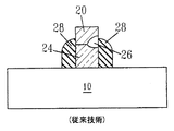
上述の問題に加えて、通常の自己整合シリサイド工程はまた、Si含有ゲート幅が70nmより薄いときに、Si含有ゲートのボイド生成の問題を引き起こす。ボイド生成の問題は図3に示される。この図において、参照番号10はSi含有基板、参照番号24はSi含有ゲート、参照番号20はSi含有ゲート24上に形成されたコバルト・ジシリサイド膜、参照番号26はSi含有ゲート24内のボイド、参照番号28はSi含有ゲート24の側壁上に存在する絶縁体スペーサである。上述され、図3に描かれたボイド生成の問題は、Si含有ゲート24の抵抗を増加させる。
In addition to the above problems, the normal self-aligned silicide process also causes Si-containing gate voiding problems when the Si-containing gate width is less than 70 nm. The problem of void generation is illustrated in FIG. In this figure,
通常の自己整合シリサイド工程における最近の改善は、同一出願人に譲渡されたBrodsky他による特許文献1に記載されている。具体的には、Brodsky他により開示された工程は、電気的に接触されるべき電子デバイスを含むシリコン含有基板上に、約30原子%より少ないSiを含み、残りがCo及び/又はNiである金属シリコン合金層を形成するステップと、金属シリコン合金又は純金属に比べて実質的にエッチング不可能な金属リッチのシリサイド層を形成するために、約300℃から約500℃までの温度で金属シリコン合金層をアニール処理する第1のアニール・ステップと、非シリコン領域上のあらゆる未反応金属シリコン合金を選択的に除去するステップと、最低抵抗相にある金属シリサイド相を形成するのに効果的な条件下で金属リッチのシリサイド層をアニール処理する第2のアニール・ステップとを含む。随意的な酸素拡散バリヤ層を、第1のアニール・ステップの前に、金属シリコン合金層の上に形成することができる。 A recent improvement in a conventional self-aligned silicide process is described in US Pat. Specifically, the process disclosed by Brodsky et al. Includes less than about 30 atomic percent Si on the silicon-containing substrate containing the electronic device to be electrically contacted with the remainder being Co and / or Ni. Forming a metal silicon alloy layer and metal silicon at a temperature from about 300 ° C. to about 500 ° C. to form a metal-rich silicide layer that is substantially non-etchable compared to a metal silicon alloy or pure metal. Effective to form a first annealing step for annealing the alloy layer, selectively removing any unreacted metal silicon alloy on the non-silicon region, and forming a metal silicide phase in the lowest resistance phase. A second annealing step of annealing the metal rich silicide layer under conditions. An optional oxygen diffusion barrier layer can be formed on the metal silicon alloy layer prior to the first annealing step.
Brodsky他によって説明された工程は、第1のアニール・ステップにおいて、通常の自己整合シリサイド工程に関して上述された双方向拡散機構とは異なる拡散機構を受ける。特に、Brodsky他によって開示された工程においては、Coだけが下方に拡散して金属リッチのシリサイド層を形成する。結果として得られ、Brodsky他の工程を用いて達成される一方向機構が図4に示される。この図において、参照番号10はSi含有材料、参照番号30は金属シリコン合金層、参照番号14は自然酸化物層、そして参照番号18はCoの拡散方向を示す。
The process described by Brodsky et al. Undergoes a different diffusion mechanism in the first annealing step than the bidirectional diffusion mechanism described above with respect to the normal self-aligned silicide process. In particular, in the process disclosed by Brodsky et al., Only Co diffuses downward to form a metal-rich silicide layer. The resulting one-way mechanism achieved using the Brodsky et al. Process is shown in FIG. In this figure,
通常の自己整合シリサイド工程と同様に、Brodsky他によって開示された工程においては、第1アニール・ステップの後、あらゆる未反応のCo金属が除去される。Brodsky他のカラム5、19行−21行に示されるように、金属リッチのシリサイド相に変換されなかった‘残留’Coを除去するためのエッチャントとして、過酸化水素と硫酸の混合物を用いることができる。このエッチング工程の間に、Co金属中のSiは酸化されて金属リッチのシリサイドの上にSiO2表面層を形成する。その構造体は、例えば図5に示され、参照番号32は金属リッチのシリサイド相、参照番号22は表面SiO2層を示す。
Similar to the normal self-aligned silicide process, in the process disclosed by Brodsky et al., Any unreacted Co metal is removed after the first annealing step. As shown in Brodsky et al. Column 5, lines 19-21, a mixture of hydrogen peroxide and sulfuric acid may be used as an etchant to remove 'residual' Co that has not been converted to a metal-rich silicide phase. it can. During this etching process, Si in the Co metal is oxidized to form a SiO 2 surface layer on the metal-rich silicide. The structure is shown, for example, in FIG. 5, where reference number 32 indicates a metal-rich silicide phase and
次に、Brodsky他の工程において、金属リッチのシリサイドをコバルト・ジシリサイドに変換する第2のアニールが実施される。第2のアニールは、約600℃から約900℃までの温度で実施される。 Next, in a Brodsky et al. Process, a second anneal is performed to convert the metal rich silicide to cobalt disilicide. The second anneal is performed at a temperature from about 600 ° C. to about 900 ° C.
Brodsky他によって開示された工程を利用して達成される一方向拡散機構には、双方向拡散が起きる通常の自己整合シリサイド工程と比較して、いくつかの利点がある。第1に、自然酸化物上の過剰なCo金属がエッチング除去されるため、結果として生じるコバルト・ジシリサイド膜内にはSiO2の析出物はなく、このことが低シート抵抗をもたらす。第2に、一方向拡散では、Si内へのCoの拡散だけが生じ、Siは拡散しないため、狭いSi含有ゲートに伴うボイド生成の問題はない。 The unidirectional diffusion mechanism achieved using the process disclosed by Brodsky et al. Has several advantages compared to the normal self-aligned silicide process where bi-directional diffusion occurs. First, because excess Co metal on the native oxide is etched away, there is no SiO 2 deposit in the resulting cobalt disilicide film, which results in low sheet resistance. Second, in unidirectional diffusion, only Co diffusion into Si occurs, and Si does not diffuse, so there is no problem of void generation associated with a narrow Si-containing gate.
Brodsky他によって開示された工程によって達成される改善にもかかわらず、Brodsky他の工程は、自己制限的なCo拡散深度をもたらす。例えば、第1アニール・ステップにおいて、約3nmのコバルトリッチのシリサイド膜が形成される。剥離後及び第2アニールにより、3nmのコバルトリッチのシリサイドは、12nmのコバルト・ジシリサイド膜に変換される。通常の相補形金属酸化物半導体(CMOS)加工工程においては、接触反応性イオン・エッチング及びスパッタ洗浄のステップは、典型的には約10nmから約12nmまでのコバルト・ジシリサイドを、Brodsky他によって開示された工程に関してはコバルト・ジシリサイド形成の境界に直角に、除去する。コバルト・ジシリサイド膜が完全に除去されるとき、金属から拡散コンタクトへの接触抵抗の問題が現れる。 Despite the improvements achieved by the process disclosed by Brodsky et al., Brodsky et al. Process results in a self-limiting Co diffusion depth. For example, in the first annealing step, a cobalt-rich silicide film of about 3 nm is formed. After peeling and by the second annealing, the 3 nm cobalt-rich silicide is converted into a 12 nm cobalt disilicide film. In a typical complementary metal oxide semiconductor (CMOS) processing process, contact reactive ion etching and sputter cleaning steps are typically disclosed by Brodsky et al. From about 10 nm to about 12 nm of cobalt disilicide. In the case of the above process, it is removed at right angles to the boundary of cobalt disilicide formation. When the cobalt disilicide film is completely removed, the problem of contact resistance from metal to diffusion contact appears.
ほとんどのCMOS用途において、18nmから24nmまでのコバルト・ジシリサイドのプロセス・ウィンドウの結果を有することが好ましい。通常の工程では、拡散の厚さを増加するため、シリサイド工程に用いられる第1のアニール温度を上昇させることになる。しかしながら、この場合には、最大温度は約450℃に制限されるが、その理由は(i)より高温のアニールは、トレンチ分離領域において、コバルト・シリサイド合金からコバルト・ジシリサイドの形成をもたらすことになり、それが、基板上の異なる活性領域間、即ち活性領域とSi含有ゲートの間、及び、同じ基板上の異なるSi含有ゲート間のリーク、即ち短絡をもたらすこと、そして(ii)第1アニール・ステップにおけるより高温のアニールは双方向の拡散をもたらし、それが通常の自己整合シリサイド工程において前述されたのと同じ問題をもたらすことである。 In most CMOS applications, it is preferred to have a process window result of cobalt disilicide from 18 nm to 24 nm. In a normal process, in order to increase the diffusion thickness, the first annealing temperature used in the silicide process is increased. However, in this case, the maximum temperature is limited to about 450 ° C. because (i) higher temperature annealing results in the formation of cobalt disilicide from the cobalt silicide alloy in the trench isolation region. And that leads to leakage, i.e. a short circuit, between different active regions on the substrate, i.e. between the active region and the Si-containing gate, and between different Si-containing gates on the same substrate, and (ii) a first anneal A higher temperature anneal in the step results in bidirectional diffusion, which leads to the same problems as previously described in a normal self-aligned silicide process.
上述のことを考慮すると、通常の自己整合シリサイド工程及びBrodsky他によって示されたシリサイド工程に関連する問題を回避する、金属シリサイド・コンタクトを形成する改善された方法を提供する必要性がなお存在する。 In view of the foregoing, there is still a need to provide an improved method of forming metal silicide contacts that avoids the problems associated with the conventional self-aligned silicide process and the silicide process shown by Brodsky et al. .
本発明は、Brodsky他によって開示されたシリサイド工程をさらに改善する方法を提供する。従って、Brodsky他の工程において言及された利点、すなわち、シリサイド形成中のSi消費及び短絡の低減化は、本発明においても達成される。Brodsky他によって開示された工程と比較して、本発明の方法の改善点は、結果として得られる金属シリサイドが、増加した自己制限的厚さを有することである。即ち、本発明の方法は、増加した自己制限的厚さを有する金属シリサイド・コンタクトを作成し、それによって、金属シリサイド・コンタクトに対する金属相互接続の形成中に完全には除去されない金属シリサイドを形成する方法を提供する。 The present invention provides a method for further improving the silicide process disclosed by Brodsky et al. Therefore, the advantages mentioned in the Brodsky et al. Process, i.e. the reduction of Si consumption and shorting during silicide formation, are also achieved in the present invention. Compared to the process disclosed by Brodsky et al., An improvement of the method of the present invention is that the resulting metal silicide has an increased self-limiting thickness. That is, the method of the present invention creates a metal silicide contact having an increased self-limiting thickness, thereby forming a metal silicide that is not completely removed during formation of the metal interconnect to the metal silicide contact. Provide a method.
上述の様に、Brodsky他の工程は、厚さが約12nmの金属シリサイドを与える。このような薄い金属シリサイドは、その後の相互接続工程のステップ中に、完全に又は実質的に除去されることになる。金属シリサイドの完全な又は実質的な除去は、金属から拡散コンタクトへのコンタクト抵抗の問題を引き起こす。 As mentioned above, the Brodsky et al. Process provides a metal silicide with a thickness of about 12 nm. Such thin metal silicide will be completely or substantially removed during subsequent interconnect process steps. Complete or substantial removal of the metal silicide causes contact resistance problems from the metal to the diffusion contact.
このコンタクト抵抗の問題は、本発明では、形成される金属シリサイドが、約14nmから約25nmまでの厚さ、好ましくは約18nmから約25nmまでの厚さを有する故に回避される。金属シリサイド・コンタクトの増加した厚さは、半導体産業において重要であり、その理由は、シリサイド・コンタクトの内部に完全に埋め込まれた低位部分(側壁及び底壁を含む)を有する金属シリサイド・コンタクトへの金属コンタクトの形成のための余裕を見込んでいるためである。 This contact resistance problem is avoided in the present invention because the metal silicide formed has a thickness from about 14 nm to about 25 nm, preferably from about 18 nm to about 25 nm. The increased thickness of the metal silicide contact is important in the semiconductor industry because the metal silicide contact has a lower portion (including sidewalls and bottom wall) that is completely embedded inside the silicide contact. This is because a margin for forming the metal contact is expected.
さらに、本発明の方法は、低リークを示す厚い金属シリサイドを含む構造体を提供する。「低リーク」により、構造体内に存在するトレンチ分離領域の上に生ずる金属シリサイドが、殆ど又は全くないことを意味する。 Furthermore, the method of the present invention provides a structure comprising a thick metal silicide exhibiting low leakage. By “low leakage” is meant that there is little or no metal silicide formed on the trench isolation region present in the structure.
本発明は上記の事柄を、Brodsky他により開示された金属シリコン合金を用いることによって、そして、2つの別個の熱サイクルが実施される第1のアニールを利用することによって達成する。本発明によれば、第1アニールの第1熱サイクルは、Si含有層内への、Co、Ni、又は、Co及びNiのような耐火金属(高融点金属)の一方向拡散を増強することが可能な温度で実施される。第1熱サイクルは、アモルファス金属(例えば、Co、Ni、又は、Co及びNi)含有シリサイドの形成を引き起こす。第1アニールの第2熱サイクルは、アモルファス金属含有シリサイドを、金属含有シリコン合金層又は純金属含有層に比べて、実質的にエッチング不可能な結晶化された金属リッチのシリサイドに転化する温度で実施される。上述の2つの熱サイクルを含む第1アニールの後に、あらゆる未反応の金属含有シリコン合金層を構造体から除去するために、選択的エッチングが実施される。第2のアニールは、第1アニールの2つの熱サイクルによって形成された金属リッチ・シリサイド相を、最低抵抗相にある金属シリサイド相に転化するために実施される。Co、Ni及びこれらの合金は、シリサイド・コンタクトを形成することに用いられた金属として具体的に言及されているが、例えばPtなどの他の耐火金属(高融点金属)もここで考慮されている。 The present invention accomplishes the above by using a metal silicon alloy disclosed by Brodsky et al. And by utilizing a first anneal in which two separate thermal cycles are performed. According to the present invention, the first thermal cycle of the first anneal enhances unidirectional diffusion of refractory metals (refractory metals) such as Co, Ni, or Co and Ni into the Si-containing layer. Is carried out at a possible temperature. The first thermal cycle causes the formation of an amorphous metal (eg, Co, Ni, or Co and Ni) containing silicide. The second thermal cycle of the first anneal is at a temperature that converts the amorphous metal-containing silicide into a crystallized metal-rich silicide that is substantially non-etchable compared to a metal-containing silicon alloy layer or a pure metal-containing layer. To be implemented. After the first anneal including the two thermal cycles described above, a selective etch is performed to remove any unreacted metal-containing silicon alloy layer from the structure. The second anneal is performed to convert the metal rich silicide phase formed by the two thermal cycles of the first anneal to a metal silicide phase in the lowest resistance phase. Co, Ni and their alloys are specifically mentioned as the metals used to form the silicide contacts, but other refractory metals (refractory metals) such as Pt are also considered here. Yes.
概略的には、本発明の方法は、Si含有材料上に金属含有シリコン合金層を含む構造体を準備するステップと、前記の構造体に、前記のSi含有材料内への前記の金属の一方向拡散を増強し、それによってアモルファス金属含有シリサイドを形成する第1の温度で実施される第1の熱サイクル、及び、アモルファス金属含有シリサイドを、金属含有シリコン合金層に比べて実質的にエッチング不可能な結晶化金属リッチ・シリサイドに転化する第2の温度で実施される第2の熱サイクルを含む第1のアニールを施すステップと、あらゆる未反応の金属含有シリコン合金層を構造体から除去するステップと、前記の構造体に、前記の結晶化金属リッチ・シリサイドを最低抵抗相にある金属シリサイド相に転化する第3の温度において第2のアニールを施すステップとを含む。 In general, the method of the present invention comprises the steps of providing a structure comprising a metal-containing silicon alloy layer on a Si-containing material, and providing the structure with one of the metals in the Si-containing material. A first thermal cycle performed at a first temperature that enhances directional diffusion and thereby forms an amorphous metal-containing silicide, and the amorphous metal-containing silicide is substantially less etched compared to the metal-containing silicon alloy layer. Applying a first anneal that includes a second thermal cycle performed at a second temperature that converts to a possible crystallized metal rich silicide, and removing any unreacted metal-containing silicon alloy layer from the structure. And a second temperature at the third temperature at which the crystallized metal-rich silicide is converted to a metal silicide phase in the lowest resistance phase. And a step of subjecting Le.
上述の方法において、金属含有シリコン合金層の金属は、金属シリサイドを形成するようにシリコンと反応することが可能な任意の耐火金属(高融点金属)又は耐火金属(高融点金属)合金を含む。好ましい金属は、Co、Ni又はそれらの合金である。
酸素拡散を阻止する随意的なバリヤ層を、第1アニールの前に金属含有シリコン合金層上に形成することができる。
In the above method, the metal of the metal-containing silicon alloy layer comprises any refractory metal (refractory metal) or refractory metal (refractory metal) alloy capable of reacting with silicon to form a metal silicide. Preferred metals are Co, Ni or their alloys.
An optional barrier layer that prevents oxygen diffusion can be formed on the metal-containing silicon alloy layer prior to the first anneal.
Niが金属として使用されるときには、Niリッチのシリサイド相が、第1アニールの後に形成される。除去ステップ後に行われる第2アニールは、Niリッチのシリサイド相を、Niシリサイドの最低抵抗相であるNiモノシリサイドに転化する。他方、Coが使用されるときには、第1アニールは、Co−Si合金層をCoリッチのシリサイド層に転化し、第2アニールは、除去ステップ後、金属リッチ・シリサイド相を、Coシリサイドの最低抵抗相であるCoジシリサイド相に転化する。 When Ni is used as the metal, a Ni-rich silicide phase is formed after the first anneal. The second annealing performed after the removal step converts the Ni-rich silicide phase to Ni monosilicide, which is the lowest resistance phase of Ni silicide. On the other hand, when Co is used, the first anneal converts the Co—Si alloy layer to a Co-rich silicide layer, and the second anneal, after the removal step, converts the metal-rich silicide phase into the lowest resistance of Co silicide. The phase is converted to a Co disilicide phase.
図6−図11を参照すると、Si消費及び短絡が十分に低減された低抵抗の厚い金属シリサイドを含むCMOS構造体を形成することが可能な基本工程ステップが示されている。「厚い」によって、約14nmから約25nmまでの厚さを有する金属シリサイドを意味する。具体的には、図6は、第1のステップが実施された後に形成される最初の構造体50を示す。具体的には、構造体50は、その上に金属含有シリコン合金層56を有するSi含有材料52を含む。Si含有材料52は、Si含有基板、ゲート電極又はその両方とすることができ、Si含有材料52は、特にそれが基板である場合、合金層56の堆積の前に存在し、合金層56とSi含有材料52との間の界面54となる表面酸化物層を随意に含むことができる。
Referring to FIGS. 6-11, basic process steps are shown that can form a CMOS structure comprising a low resistance thick metal silicide with sufficiently reduced Si consumption and shorting. By “thick” is meant a metal silicide having a thickness from about 14 nm to about 25 nm. Specifically, FIG. 6 shows the
層52として用いることのできる適切なSi含有材料は、単結晶Si、多結晶Si、SiGe、アモルファスSi、シリコン・オン・インシュレータ(SOI)、シリコン・ゲルマニウム・オン・インシュレータ(SGOI)及び他の類似のSi含有材料を含むがそれらに限定はされない。Si含有材料52はドープしても、ドープしなくともよく、様々な分離領域及びデバイス領域を含むことができる。これらの領域は、図面には示されていないが、やはりSi含有材料52の中に含まれることが意図されている。
Suitable Si-containing materials that can be used as
Si含有材料52が基板として機能するとき、Si含有材料52は、例えば電界効果トランジスタ(EFT)のような少なくとも1つの電気的デバイスを含む。この実施形態においては、金属シリサイドは、EFTのソース/ドレイン拡散部を含む基板の領域内に形成される。Si含有材料52がゲート電極として機能するときには、金属シリサイドは、ゲート電極の上に形成することもできる。
When the Si-containing
随意的な表面酸化物層が存在するときは、それは約0.1nmから約0.3nmまでの厚さを有する薄い酸化物である。本発明の一実施形態において、表面酸化物層は、本発明の方法を使用する前に、構造体50から完全に除去される。この実施形態においては、その上に金属含有シリコン(Si)合金層56を形成する前に、構造体50から表面酸化物層を完全に除去するためにHFを用いることができる。
When an optional surface oxide layer is present, it is a thin oxide having a thickness from about 0.1 nm to about 0.3 nm. In one embodiment of the present invention, the surface oxide layer is completely removed from the
金属含有シリコン合金層56は、当業者には公知である通常の堆積工程を用いて、Si含有材料52の表面上に(又は、随意的表面酸化物層が存在する場合には、その上に)形成される。例えば、金属含有Si合金層56は、化学気相堆積法、プラズマ化学気相堆積法、蒸発法、スパッタリング法及び他の同様の堆積工程によって、堆積することができる。これらの方法の中で、通常はスパッタリング法が金属含有Si合金層56の形成に用いられる。代替的に、金属含有Si合金層56は、初めにSi含有材料52の表面上に金属層を堆積させ、その後に、イオン注入法又は別の同様のドープ工程を用いて、少なくともSiで金属層をドープすることによって、形成することができる。
The metal-containing
金属含有シリコン合金層56は、シリコン、及び、シリコンと反応するときに金属シリサイドを形成することができる耐火金属(高融点金属)又は金属合金を含む。層56内の金属は、Co、Ni及びそれらの混合物から構成される群から選択されることが好ましい。従って、好ましい実施形態においては、金属含有シリコン合金層56は、Co−Si合金、Ni−Si合金、又はCo−Ni−Siのような金属の混合物を含むことができる。好ましい合金のうち、金属含有シリコン合金層56はCo−Si合金を含むことが極めて好ましい。本発明によれば、金属含有シリコン合金層56は、典型的には、約30原子%より少ないSiを含む。より典型的には、シリコンは約0.1原子%から約20原子%までの量で合金層56内に存在する。
The metal-containing
金属含有シリコン合金層56の発明はまた、結果として生じるシリサイドの特性に影響を及ぼすことのできる少なくとも1つの添加物を含むことができる。合金層56中に存在することができる少なくとも1つの添加物は、例えば、シリサイドの抵抗を低下させるため、又は、シリサイドの凝集を防止するために用いることできる。本発明の合金層56の成分として用いることができる添加物の例は、C、Al、Ge、Sc、Ti、V、Cr、Mn、Fe、Cu、Y、Zr、Nb、Mo、Ru、Rh、Pd、In、Sn、La、Hf、Ta、W、Re、Ir、Pt、Ce、Pr、Nd、Sm、Eu、Gd、Tb、Dy、Ho、Er、Tm、Yb、Lu及びそれらの混合物を含むが、それらに限定はされない。これらの添加物のうち、C、Al、Ge、Sc、Ti、V、Cr、Mn、Fe、Cu、Y、Zr、Nb、Mo、Ru、Rh、Pd、In、Sn、La、Hf、Ta、W、Re、Ir、Pt及びそれらの混合物が好ましい。
The invention of the metal-containing
添加物が存在するときは、少なくとも1つの添加物は、典型的には、約0.01原子%から約50原子(at.)%までの量で合金56中に存在し、より典型的には、約0.1原子%から約20原子%までの範囲の量で存在する。少なくとも1つの合金添加物は、金蔵含有Si合金層56の堆積中又は堆積後に導入することができる。
When present, at least one additive is typically present in the
「金属含有シリコン合金」という用語は、ここでは、シリコンの均一又は不均一な分布を有する組成物、シリコンの勾配分布を有する組成物、又はそれらの混合物及び複合物を含むように用いられる。 The term “metal-containing silicon alloy” is used herein to include compositions having a uniform or non-uniform distribution of silicon, compositions having a gradient distribution of silicon, or mixtures and composites thereof.
次に、図7に示されるように、酸素拡散を阻止する随意のバリヤ層58を、金属含有シリコン合金層56の表面上に形成することができる。随意のバリヤ層58は、当業者には公知である通常の堆積工程を用いて形成することができる。随意のバリヤ層58を形成するのに用いることのできる適切な堆積工程の例証的な実施例は、化学気相堆積法、プラズマ化学気相堆積法、スパッタリング法、蒸発法、めっき法、スピン・オン・コーティング法及び他の同様の堆積工程を含むが、それらに限定はされない。随意のバリヤ層58の厚さは、随意のバリヤ層58が酸素又は別の雰囲気ガスを構造体50中へ拡散させないことができる限り、本発明には重要でない。典型的には、随意のバリヤ層58は、約10nmから約30nmまでの厚さを有する。
Next, an
随意のバリヤ層58は、酸素が構造体50中へ拡散することを妨げる、当業者には公知の通常の材料から構成される。例えば、TiN、Si3N4、TaN又は他の同様の材料は、バリヤ層58として使用することができる。図面は随意のバリヤ層58の存在を示すが、本方法は、随意のバリヤ層58が存在しない場合にも用いることができる。
第1のアニールは、図6又は図7に示される構造体に施される。完全のために、ここに描かれた図は、随意のバリヤ層58を含む構造体に施された第1アニールを示す。本発明の実施形態によれば、第1アニールは、2つの異なった熱サイクルを含む。第1熱サイクルは、合金層56からSi含有材料52への金属の一方向拡散、及び、その後のアモルファス金属含有シリサイド相の形成をもたらす。第1アニールの第1熱サイクルの後に形成される構造体は、図8に示される。具体的には、図8に示される構造体は、Si含有材料52、金属含有シリコン合金層56、アモルファス金属含有シリサイド相膜60及び随意のバリヤ層58を含む。参照番号62は金属拡散の方向を示す。
The first annealing is performed on the structure shown in FIG. 6 or FIG. For completeness, the figure depicted here shows a first anneal applied to the structure including an
第1熱サイクルは、金属の拡散を増強してアモルフファス金属シリサイド膜を形成する第1の温度T1で実施される。第1アニールの第1熱サイクルの温度は、結晶化膜の形成を引き起こさないことが重要である。本実施形態により、第1アニールの第1熱サイクルの温度が350℃より低いとき、金属拡散の増強及びアモルファス相の形成を達成することができる。第1アニールの第1熱サイクルの温度T1は、第1アニールの第2熱サイクルの温度T2より低いことに注目されたい。より典型的には、第1アニールの第1熱サイクルは、約270℃から約325℃までの温度で実施される。第1アニールの第1熱サイクルは、典型的には、約30秒から約120秒までの時間実施される。ここに例示された範囲以外の他の時間間隔も考慮されている。 The first thermal cycle is performed at a first temperature T1 that enhances metal diffusion to form an amorphous metal silicide film. It is important that the temperature of the first thermal cycle of the first annealing does not cause formation of a crystallized film. According to this embodiment, when the temperature of the first thermal cycle of the first annealing is lower than 350 ° C., enhanced metal diffusion and formation of an amorphous phase can be achieved. Note that the temperature T1 of the first thermal cycle of the first anneal is lower than the temperature T2 of the second thermal cycle of the first anneal. More typically, the first thermal cycle of the first anneal is performed at a temperature from about 270 ° C. to about 325 ° C. The first thermal cycle of the first anneal is typically performed for a period of about 30 seconds to about 120 seconds. Other time intervals outside the range illustrated here are also considered.
次に、図8に示される構造体は、アモルファス金属含有シリサイド相膜60を結晶化金属リッチ・シリサイド相膜64(図9参照)に転化する温度で実施される第2の熱サイクル(なお本明細書の用語に従って、第1アニールに伴うものと考えられる)を施される。
Next, the structure shown in FIG. 8 includes a second thermal cycle (note that the amorphous metal-containing
第1アニールの第2熱サイクルは、450℃より低く、まだT1よりは高い第2の温度T2で実施される。より典型的には、第1アニールの第2熱サイクルは、約350℃から約400℃までの温度で実施される。第1アニールの第2熱サイクルは、典型的には、約10秒から約30秒までの時間実施される。第1アニールの第2熱サイクルが第1熱サイクルよりも短い、即ち、時間2<時間1である限り、ここに例示された範囲以外の他の時間間隔も考慮されている。 The second thermal cycle of the first anneal is performed at a second temperature T2 that is lower than 450 ° C. and still higher than T1. More typically, the second thermal cycle of the first anneal is performed at a temperature from about 350 ° C. to about 400 ° C. The second thermal cycle of the first anneal is typically performed for a period of about 10 seconds to about 30 seconds. As long as the second thermal cycle of the first anneal is shorter than the first thermal cycle, i.e., time 2 <time 1, other time intervals outside the range illustrated here are also considered.
第1アニールの上記の2つの異なる熱サイクルは、例えば、He、Ar、Ne又はフォーミング・ガスの同じ又は異なるガス雰囲気中で実施される高速熱アニール(RTA)工程である。従って、第1アニールはまた、高速熱アニール・ステップであると考えることができる。第1アニールの第2熱サイクルは、第1熱サイクルの直後に、熱サイクルの間の如何なる冷却もなしに実施することができ、又は、T1から室温まで冷却した後の任意の時間に実施することができる。 The above two different thermal cycles of the first anneal are rapid thermal anneal (RTA) processes performed in the same or different gas atmosphere of, for example, He, Ar, Ne or forming gas. Thus, the first anneal can also be considered a rapid thermal anneal step. The second thermal cycle of the first anneal can be performed immediately after the first thermal cycle, without any cooling during the thermal cycle, or at any time after cooling from T1 to room temperature. be able to.
第1アニールの間に、金属含有シリコン合金層56の全てが消費される可能性、又は、代替的に、合金層56の一部がアニール後に残る可能性がある。この後の方の実施形態は図9に示される。さらに、第1アニールが完了した後、表面酸化物層が、金属リッチ・シリサイド膜64中に存在することになる。
During the first anneal, all of the metal-containing
上記の条件が、出発の金属含有シリコン合金56又は純金属に比べて実質的にエッチング不可能な、金属リッチ・シリサイド層64を形成し、そのため、このエッチング不可能な金属リッチ・シリサイド層を生ずる通常の自己適合シリサイド工程に一般的に用いられる、より高温のアニール温度が回避されることに注目されたい。Brodsky他によって以前に報告されたように、金属含有シリコン合金の使用は、従来技術の工程に利用可能であるよりも低い温度で、金属リッチ・シリサイド層の形成を可能にする。より低い温度が金属リッチ・シリサイド層の形成に用いられるため、短絡発生の傾向が激減する。さらに、最初の合金膜56がシリコンを含むため、シリコン消費の減少が本実施形態の方法を用いて観察される。
The above conditions form a metal
前述の2つの異なる熱サイクルを含む第1アニールの後、随意のバリヤ層58及びあらゆる残留金属含有シリコン合金層56(又は、任意の純金属層)は、当業者には公知の通常のエッチング法を用いて、構造体から選択的に除去される(図10参照)。
After the first anneal including the two different thermal cycles described above, the
例えば、任意の湿式エッチング工程は、随意のバリヤ層58及び金属含有シリコン合金層56を、構造体から除去するのに用いることができる。湿式エッチング工程に用いられる化学エッチャントは、金属リッチ・シリサイド層(又は膜)64に比べて、バリヤ層58及び金属含有シリコン合金層56を除去するのに高度に選択的でなければならない。本発明において用いることができる適切なエッチャントは、過酸化水素と硝酸又は硫酸の混合物である。他の化学エッチャントもまた、本発明において用いることができる。図10は、湿式エッチング工程後に形成される表面酸化物層66の存在を示す。表面酸化物層66は、約1nmから約5nmまでの厚さを有する薄層である。
For example, an optional wet etch process can be used to remove the
構造体から随意のバリヤ層58及びあらゆる残留金属含有シリコン合金層56を除去するのに、乾式エッチング工程を用いることもまた本発明の構想内にある。乾式エッチング工程は、表面酸化物層66の形成を回避する。ここで用いることができる適切な乾式エッチング法は、反応性イオン・エッチング、イオン・ビーム・エッチング、プラズマ・エッチング及び他の同様の乾式エッチング法を含むが、それらに限定はされない。
It is also within the concept of the present invention to use a dry etch process to remove the
随意のバリヤ層58及びあらゆる未反応の金属含有シリコン合金層56を構造体から除去した後、金属リッチ・シリサイド層64を、例えば、Coジシリサイド又はNiモノシリサイドの最低抵抗の金属シリサイド相に転化するために、本発明においては第2のアニールが用いられる。第2アニールは、第1アニールにおいて用いられた温度よりも高い第3の温度T3(即ち、T3は、T1及びT2よりも高い)で実施される。上述のように、第2アニールは、金属リッチ層64を、金属の最低抵抗のシリサイド相を有するシリサイド層68に転化するのに効果的な条件の下で実施される(図11参照)。本発明のこのステップが実施された後に、表面酸化物層66が構造体中に残ることに注目されたい。表面酸化物層66は、その後の工程ステップで当業者には公知の方法を用いて、構造体から除去することができる
After removal of the
この第2アニールは、ガス雰囲気を用いてRTAによっても実施される。典型的には、第2アニールは、約600℃から約900℃までの温度で、約300秒又はそれ以下の時間、連続加熱方式、又はランプ・ソーク加熱方式を用いて実施される。選択された条件が例えば、Co又はNiの耐火金属(高融点金属)の最低抵抗シリサイド相が構造体中に形成されるように第1アニール温度よりも高温である限り、他の温度及び時間もここで考慮されている。 This second annealing is also performed by RTA using a gas atmosphere. Typically, the second anneal is performed at a temperature from about 600 ° C. to about 900 ° C., for a time of about 300 seconds or less, using a continuous heating method or a lamp / soak heating method. As long as the selected conditions are higher than the first annealing temperature so that the lowest resistance silicide phase of, for example, a Co or Ni refractory metal (refractory metal) is formed in the structure, other temperatures and times are also possible. Is considered here.
本発明は次の3つの利点、即ち、Si消費の実質的な削減、短絡発生傾向の劇減、及びBrodsky他により開示された工程から得られるよりも厚い、例えばCo及び/又はNiの最低抵抗相における金属シリサイド、をもたらすことを再度強調する。上記のように、Brodsky他の特許において形成される結果として得られる金属シリサイドは約12nmであり、一方、本発明において形成される金属シリサイドは、約14nmから約25nmまでの厚さを有する。より典型的には、本実施形態において形成される金属シリサイドは、約18nmから約25nmまでの厚さを有する。 The present invention has the following three advantages: a substantial reduction in Si consumption, a drastic reduction in the tendency to short circuit, and a minimum resistance, eg, Co and / or Ni, that is thicker than obtained from the process disclosed by Brodsky et al. It is emphasized again that it results in metal silicide in the phase. As noted above, the resulting metal silicide formed in the Brodsky et al. Patent is about 12 nm, while the metal silicide formed in the present invention has a thickness from about 14 nm to about 25 nm. More typically, the metal silicide formed in this embodiment has a thickness from about 18 nm to about 25 nm.
上述の方法から結果として生ずる構造体は、従って、例えば、Coジシリサイド又はNiモノシリサイドなど、最低抵抗相にある金属シリサイドの層68を含む領域を有するSi含有材料52を含む。
The resulting structure from the above method thus includes a Si-containing
本発明は、その好ましい実施形態に関して特に図示され説明されてきたが、本発明の範囲を逸脱することなく、形状及び細部における前述及び他の変更を施すことができることを、当業者は理解するであろう。従って、本発明は、説明され図示された正確な形状及び細部には限定されず、添付の請求項の範囲内に含まれることが意図されている。 While the invention has been particularly shown and described with respect to preferred embodiments thereof, those skilled in the art will appreciate that the foregoing and other changes in shape and detail may be made without departing from the scope of the invention. I will. Accordingly, the invention is not limited to the precise forms and details described and illustrated, but is intended to be included within the scope of the following claims.
Claims (19)
Si含有材料の上に金属含有シリコン合金層を含む構造体を準備するステップと、
前記構造体に、前記Si含有材料中への前記金属の一方向拡散を増強してアモルファス金属含有シリサイドを形成する第1の温度で実施される第1の熱サイクルと、前記アモルファス金属含有シリサイドを、前記金属含有シリコン合金層に比べて実質的にエッチング不可能な結晶化金属リッチ・シリサイドに転化する第2の温度で実施される第2の熱サイクルとを含む第1のアニール処理を施すステップと、
あらゆる未反応金属含有シリコン合金層を前記構造体から除去するステップと、
前記構造体に、前記結晶化金属リッチ・シリサイドを最低抵抗相にある金属シリサイド相に転化する第3の温度で第2のアニール処理を施すステップと
を含む方法。 A method of forming a metal silicide on a surface of a Si-containing material, comprising:
Providing a structure including a metal-containing silicon alloy layer on a Si-containing material;
A first thermal cycle performed at a first temperature that enhances unidirectional diffusion of the metal into the Si-containing material to form an amorphous metal-containing silicide; and the amorphous metal-containing silicide. Applying a first annealing process including a second thermal cycle performed at a second temperature that converts to a crystallized metal rich silicide that is substantially non-etchable compared to the metal-containing silicon alloy layer. When,
Removing any unreacted metal-containing silicon alloy layer from the structure;
Subjecting the structure to a second annealing treatment at a third temperature that converts the crystallized metal rich silicide to a metal silicide phase in the lowest resistance phase.
Applications Claiming Priority (2)
| Application Number | Priority Date | Filing Date | Title |
|---|---|---|---|
| US10/711,365 US7208414B2 (en) | 2004-09-14 | 2004-09-14 | Method for enhanced uni-directional diffusion of metal and subsequent silicide formation |
| PCT/EP2005/054087 WO2006029950A1 (en) | 2004-09-14 | 2005-08-18 | Uni-directional diffusion of metal silicide in semiconductor devices |
Publications (2)
| Publication Number | Publication Date |
|---|---|
| JP2008513977A true JP2008513977A (en) | 2008-05-01 |
| JP2008513977A5 JP2008513977A5 (en) | 2010-09-09 |
Family
ID=35170075
Family Applications (1)
| Application Number | Title | Priority Date | Filing Date |
|---|---|---|---|
| JP2007530694A Withdrawn JP2008513977A (en) | 2004-09-14 | 2005-08-18 | Unidirectional diffusion of metal silicide in semiconductor devices. |
Country Status (7)
| Country | Link |
|---|---|
| US (2) | US7208414B2 (en) |
| EP (1) | EP1800332A1 (en) |
| JP (1) | JP2008513977A (en) |
| KR (1) | KR20070053234A (en) |
| CN (1) | CN100505168C (en) |
| TW (1) | TW200616051A (en) |
| WO (1) | WO2006029950A1 (en) |
Cited By (2)
| Publication number | Priority date | Publication date | Assignee | Title |
|---|---|---|---|---|
| JP2006147897A (en) * | 2004-11-22 | 2006-06-08 | Samsung Electronics Co Ltd | Method of manufacturing semiconductor apparatus |
| JP2007067225A (en) * | 2005-08-31 | 2007-03-15 | Toshiba Corp | Semiconductor device and manufacturing method therefor |
Families Citing this family (23)
| Publication number | Priority date | Publication date | Assignee | Title |
|---|---|---|---|---|
| US7238611B2 (en) * | 2005-04-13 | 2007-07-03 | United Microelectronics Corp. | Salicide process |
| KR100715267B1 (en) * | 2005-06-09 | 2007-05-08 | 삼성전자주식회사 | Stacked semiconductor device and method for manufacturing the same |
| US7419907B2 (en) * | 2005-07-01 | 2008-09-02 | International Business Machines Corporation | Eliminating metal-rich silicides using an amorphous Ni alloy silicide structure |
| US7538029B2 (en) * | 2005-07-06 | 2009-05-26 | International Business Machines Corporation | Method of room temperature growth of SiOx on silicide as an etch stop layer for metal contact open of semiconductor devices |
| JP4755894B2 (en) * | 2005-12-16 | 2011-08-24 | 株式会社東芝 | Semiconductor device and manufacturing method thereof |
| US7485572B2 (en) * | 2006-09-25 | 2009-02-03 | International Business Machines Corporation | Method for improved formation of cobalt silicide contacts in semiconductor devices |
| US7622386B2 (en) * | 2006-12-06 | 2009-11-24 | International Business Machines Corporation | Method for improved formation of nickel silicide contacts in semiconductor devices |
| US7553762B2 (en) * | 2007-02-09 | 2009-06-30 | United Microelectronics Corp. | Method for forming metal silicide layer |
| JP5214261B2 (en) * | 2008-01-25 | 2013-06-19 | ルネサスエレクトロニクス株式会社 | Manufacturing method of semiconductor device |
| KR101384111B1 (en) * | 2009-01-09 | 2014-04-10 | 주식회사 에스앤에스텍 | A Blank Mask, A Photomask using the Same and Method of Fabricating the Same |
| JP5332947B2 (en) * | 2009-06-25 | 2013-11-06 | 富士通セミコンダクター株式会社 | Manufacturing method of semiconductor device |
| US8021982B2 (en) | 2009-09-21 | 2011-09-20 | International Business Machines Corporation | Method of silicide formation by adding graded amount of impurity during metal deposition |
| CN102044422B (en) * | 2009-10-19 | 2012-07-04 | 中芯国际集成电路制造(上海)有限公司 | Method for forming self-aligned metallic silicide |
| CN102110624B (en) * | 2009-12-23 | 2012-05-30 | 中芯国际集成电路制造(上海)有限公司 | Method for detecting nickel and platinum removing device |
| CN101764058B (en) * | 2009-12-31 | 2013-07-31 | 复旦大学 | Method for forming ultrathin controllable metal silicide |
| US8304319B2 (en) * | 2010-07-14 | 2012-11-06 | Taiwan Semiconductor Manufacturing Company, Ltd. | Method for making a disilicide |
| CN102427052B (en) * | 2011-11-03 | 2013-12-18 | 上海新傲科技股份有限公司 | Silicon-on-insulator (SOI) material substrate with high-efficiency recombination center and preparation method for silicon-on-insulator (SOI) material substrate |
| CN103137462B (en) * | 2011-11-25 | 2015-11-25 | 中芯国际集成电路制造(上海)有限公司 | The formation method of self-aligned metal silicate |
| CN104934468B (en) * | 2014-03-17 | 2018-07-20 | 中芯国际集成电路制造(上海)有限公司 | Grid and preparation method thereof |
| US9865466B2 (en) * | 2015-09-25 | 2018-01-09 | Applied Materials, Inc. | Silicide phase control by confinement |
| JP2018078212A (en) * | 2016-11-10 | 2018-05-17 | 三重富士通セミコンダクター株式会社 | Method for manufacturing semiconductor device |
| US10453750B2 (en) | 2017-06-22 | 2019-10-22 | Globalfoundries Inc. | Stacked elongated nanoshapes of different semiconductor materials and structures that incorporate the nanoshapes |
| CN112585763B (en) * | 2020-11-27 | 2024-04-05 | 英诺赛科(苏州)半导体有限公司 | Semiconductor device and method for manufacturing the same |
Family Cites Families (13)
| Publication number | Priority date | Publication date | Assignee | Title |
|---|---|---|---|---|
| US5027185A (en) * | 1988-06-06 | 1991-06-25 | Industrial Technology Research Institute | Polycide gate FET with salicide |
| US5536684A (en) * | 1994-06-30 | 1996-07-16 | Intel Corporation | Process for formation of epitaxial cobalt silicide and shallow junction of silicon |
| US5780361A (en) | 1995-06-23 | 1998-07-14 | Nec Corporation | Salicide process for selectively forming a monocobalt disilicide film on a silicon region |
| US5780362A (en) * | 1996-06-04 | 1998-07-14 | Wang; Qingfeng | CoSi2 salicide method |
| US6022801A (en) * | 1998-02-18 | 2000-02-08 | International Business Machines Corporation | Method for forming an atomically flat interface for a highly disordered metal-silicon barrier film |
| US6413859B1 (en) * | 2000-03-06 | 2002-07-02 | International Business Machines Corporation | Method and structure for retarding high temperature agglomeration of silicides using alloys |
| US6323130B1 (en) * | 2000-03-06 | 2001-11-27 | International Business Machines Corporation | Method for self-aligned formation of silicide contacts using metal silicon alloys for limited silicon consumption and for reduction of bridging |
| US6251779B1 (en) * | 2000-06-01 | 2001-06-26 | United Microelectronics Corp. | Method of forming a self-aligned silicide on a semiconductor wafer |
| US6605513B2 (en) * | 2000-12-06 | 2003-08-12 | Advanced Micro Devices, Inc. | Method of forming nickel silicide using a one-step rapid thermal anneal process and backend processing |
| US6444578B1 (en) * | 2001-02-21 | 2002-09-03 | International Business Machines Corporation | Self-aligned silicide process for reduction of Si consumption in shallow junction and thin SOI electronic devices |
| JP3515556B2 (en) * | 2001-12-04 | 2004-04-05 | 株式会社東芝 | Programmable element, programmable circuit and semiconductor device |
| US6657244B1 (en) * | 2002-06-28 | 2003-12-02 | International Business Machines Corporation | Structure and method to reduce silicon substrate consumption and improve gate sheet resistance during silicide formation |
| US6905560B2 (en) * | 2002-12-31 | 2005-06-14 | International Business Machines Corporation | Retarding agglomeration of Ni monosilicide using Ni alloys |
-
2004
- 2004-09-14 US US10/711,365 patent/US7208414B2/en not_active Expired - Fee Related
-
2005
- 2005-08-18 WO PCT/EP2005/054087 patent/WO2006029950A1/en active Application Filing
- 2005-08-18 EP EP05774200A patent/EP1800332A1/en not_active Withdrawn
- 2005-08-18 CN CNB2005800246778A patent/CN100505168C/en not_active Expired - Fee Related
- 2005-08-18 KR KR1020077004641A patent/KR20070053234A/en active IP Right Grant
- 2005-08-18 JP JP2007530694A patent/JP2008513977A/en not_active Withdrawn
- 2005-09-09 TW TW094131071A patent/TW200616051A/en unknown
-
2007
- 2007-02-07 US US11/672,363 patent/US20070128867A1/en not_active Abandoned
Cited By (2)
| Publication number | Priority date | Publication date | Assignee | Title |
|---|---|---|---|---|
| JP2006147897A (en) * | 2004-11-22 | 2006-06-08 | Samsung Electronics Co Ltd | Method of manufacturing semiconductor apparatus |
| JP2007067225A (en) * | 2005-08-31 | 2007-03-15 | Toshiba Corp | Semiconductor device and manufacturing method therefor |
Also Published As
| Publication number | Publication date |
|---|---|
| US7208414B2 (en) | 2007-04-24 |
| CN1989598A (en) | 2007-06-27 |
| TW200616051A (en) | 2006-05-16 |
| EP1800332A1 (en) | 2007-06-27 |
| WO2006029950A1 (en) | 2006-03-23 |
| KR20070053234A (en) | 2007-05-23 |
| CN100505168C (en) | 2009-06-24 |
| US20060057844A1 (en) | 2006-03-16 |
| US20070128867A1 (en) | 2007-06-07 |
Similar Documents
| Publication | Publication Date | Title |
|---|---|---|
| JP2008513977A (en) | Unidirectional diffusion of metal silicide in semiconductor devices. | |
| CN101432860B (en) | Method for forming self-aligned metal silicide contacts | |
| TWI321831B (en) | Method for integration of silicide contacts and silicide gate metals | |
| JP2586345B2 (en) | Semiconductor device comprising cobalt silicide film and method of manufacturing the device | |
| US8154130B2 (en) | Self-aligned metal to form contacts to Ge containing substrates and structure formed thereby | |
| JP2005019943A (en) | Nickel alloy salicide process, method for manufacturing semiconductor device using the same, nickel alloy silicide film formed therefrom and semiconductor device manufactured by using the same | |
| JP2007150293A (en) | Method for forming semiconductor structure comprising different species of silicide/germanide with cmos technique | |
| JP4146859B2 (en) | Manufacturing method of semiconductor device | |
| JP3394927B2 (en) | Method for forming metal silicide layer | |
| JPH10195643A (en) | Sputtering target, sputtering device, semiconductor device and its production | |
| JP3659330B2 (en) | Method and structure for preventing high temperature agglomeration of alloys using silicides | |
| US8580686B1 (en) | Silicidation and/or germanidation on SiGe or Ge by cosputtering Ni and Ge and using an intralayer for thermal stability | |
| US6432805B1 (en) | Co-deposition of nitrogen and metal for metal silicide formation | |
| US20060003534A1 (en) | Salicide process using bi-metal layer and method of fabricating semiconductor device using the same | |
| JP2000243726A (en) | Manufacture of semiconductor device | |
| JP5186701B2 (en) | Manufacturing method of semiconductor device | |
| JPH05315286A (en) | Electrode section of semiconductor device and its formation | |
| TW586152B (en) | Semiconductor device and manufacturing method thereof | |
| JP2900897B2 (en) | Method for manufacturing semiconductor device | |
| JP3640079B2 (en) | Manufacturing method of CMOS transistor | |
| JP4102709B2 (en) | Manufacturing method of semiconductor device | |
| JP2004363257A (en) | Method of manufacturing semiconductor device | |
| JPH10294292A (en) | Manufacture of semiconductor device | |
| JP2006100326A (en) | Process for fabricating semiconductor device, electrode film, mos transistor, and semiconductor device | |
| JPH09219514A (en) | Manufacture of semiconductor device |
Legal Events
| Date | Code | Title | Description |
|---|---|---|---|
| A521 | Written amendment |
Free format text: JAPANESE INTERMEDIATE CODE: A523 Effective date: 20080523 |
|
| A621 | Written request for application examination |
Free format text: JAPANESE INTERMEDIATE CODE: A621 Effective date: 20080523 |
|
| A521 | Written amendment |
Free format text: JAPANESE INTERMEDIATE CODE: A523 Effective date: 20100720 |
|
| A871 | Explanation of circumstances concerning accelerated examination |
Free format text: JAPANESE INTERMEDIATE CODE: A871 Effective date: 20100720 |
|
| A975 | Report on accelerated examination |
Free format text: JAPANESE INTERMEDIATE CODE: A971005 Effective date: 20100811 |
|
| A761 | Written withdrawal of application |
Free format text: JAPANESE INTERMEDIATE CODE: A761 Effective date: 20100827 |