JP2008502282A - Orthogonal frequency division multiplex receiver - Google Patents
Orthogonal frequency division multiplex receiver Download PDFInfo
- Publication number
- JP2008502282A JP2008502282A JP2007527622A JP2007527622A JP2008502282A JP 2008502282 A JP2008502282 A JP 2008502282A JP 2007527622 A JP2007527622 A JP 2007527622A JP 2007527622 A JP2007527622 A JP 2007527622A JP 2008502282 A JP2008502282 A JP 2008502282A
- Authority
- JP
- Japan
- Prior art keywords
- receiver
- demodulator
- data stream
- components
- fft
- Prior art date
- Legal status (The legal status is an assumption and is not a legal conclusion. Google has not performed a legal analysis and makes no representation as to the accuracy of the status listed.)
- Withdrawn
Links
Images


Classifications
-
- H—ELECTRICITY
- H04—ELECTRIC COMMUNICATION TECHNIQUE
- H04L—TRANSMISSION OF DIGITAL INFORMATION, e.g. TELEGRAPHIC COMMUNICATION
- H04L27/00—Modulated-carrier systems
- H04L27/26—Systems using multi-frequency codes
- H04L27/2601—Multicarrier modulation systems
- H04L27/2647—Arrangements specific to the receiver only
- H04L27/2655—Synchronisation arrangements
- H04L27/2657—Carrier synchronisation
-
- H—ELECTRICITY
- H04—ELECTRIC COMMUNICATION TECHNIQUE
- H04L—TRANSMISSION OF DIGITAL INFORMATION, e.g. TELEGRAPHIC COMMUNICATION
- H04L27/00—Modulated-carrier systems
- H04L27/26—Systems using multi-frequency codes
- H04L27/2601—Multicarrier modulation systems
- H04L27/2647—Arrangements specific to the receiver only
- H04L27/2655—Synchronisation arrangements
- H04L27/2662—Symbol synchronisation
Abstract
受信器アナログ信号をディジタル信号データ・ストリームに変換するA/D変換器(52)を含み、ディジタル信号データ・ストリームに、ガード・セグメントによって分離されたシンボルが含まれる、直交周波数分割多重信号用の受信器。この受信器に、ディジタル・データ・ストリームから複素I成分および複素Q成分の第1セットを作るI/Qデモジュレータ(54)と、I成分およびQ成分の第1セットを使用するガード・セグメント長デテクタ(58)も含まれる。この受信器に、さらに、ディジタル信号データ・ストリームから検出された長さのガード・セグメントを抽出し、除去するエクストラクタ(62)と、複素I成分および複素Q成分の第2セットを作るためにディジタル信号データ・ストリームのシンボルを復調するFFTデモジュレータ(64)が含まれる。An A / D converter (52) that converts a receiver analog signal into a digital signal data stream, the digital signal data stream including symbols separated by guard segments, for an orthogonal frequency division multiplexed signal Receiver. The receiver uses an I / Q demodulator (54) to create a first set of complex I and Q components from the digital data stream, and a guard segment length using the first set of I and Q components. A detector (58) is also included. The receiver further extracts an extracted length guard segment from the digital signal data stream and removes it (62) to create a second set of complex I and complex Q components. An FFT demodulator (64) is included that demodulates the symbols of the digital signal data stream.
Description
本願は、参照により本明細書に組み込まれている、2004年6月8日に出願した米国仮出願第60/577602号の利益を主張するものである。 This application claims the benefit of US Provisional Application No. 60 / 576,602, filed Jun. 8, 2004, which is incorporated herein by reference.
本発明は、全般的には通信受信器に関し、具体的には、直交周波数分割多重(OFDM)受信器に関する。 The present invention relates generally to communication receivers, and more particularly to orthogonal frequency division multiplexing (OFDM) receivers.
次の開示では、地上波デジタルテレビジョン(DTV)用のデジタルビデオ放送(DVB)受信器を説明する。この概念は、DTV受信器の送信のすべての他のチャネルにおよび直交周波数分割多重(OFDM)を使用する他の受信器または標準規格に同等に適用可能である。これには、無線LAN 802.11aおよび802.11g、HIPERLAN/2、Digital Audio Broadcasting(DAB)、Digital Video Broadcasting Terrestrial(DVB−T)、Digital Video Broadcasting for handheld(DVB−H)、802.16 Broadband Wireless Accessなどの国際無線標準規格を含めることができるが、これらに制限はされない。 The following disclosure describes a digital video broadcast (DVB) receiver for terrestrial digital television (DTV). This concept is equally applicable to all other channels of DTV receiver transmission and to other receivers or standards that use orthogonal frequency division multiplexing (OFDM). These include: Wireless LAN 802.11a and 802.11g, HIPERLAN / 2, Digital Audio Broadcasting (DAB), Digital Video Broadcasting Terrestrial (DVB-T), Digital VideoBroadBhDV80 International wireless standards such as Wireless Access can be included, but are not limited thereto.
欧州の地上波DTV標準規格DVB−T(ETS 300 744)は、マルチパス・フェージングと戦うためにCOFDMテクノロジに基づく。ETSI EN 300 744 V.1.4.1、「Digital Video Broadcasting(DVB):Framing Structures,channel coding,and modulation for digital terrestrial television」を参照されたい。この標準規格では、次の2つの動作モードが指定されている。
1)2048 FFTに基づき、OFDMシンボルあたり1705個の搬送波を有する2Kモード、および
2)8192 FFTに基づき、OFDMシンボルあたり6817個の搬送波を有する8Kモード。
The European terrestrial DTV standard DVB-T (ETS 300 744) is based on COFDM technology to combat multipath fading. ETSI EN 300 744 V.E. See 1.4.1, “Digital Video Broadcasting (DVB): Framing Structures, channel coding, and modulation for digital terrestrial television”. In this standard, the following two operation modes are specified.
1) 2K mode based on 2048 FFT with 1705 carriers per OFDM symbol, and 2) 8K mode based on 8192 FFT with 6817 carriers per OFDM symbol.
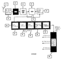
図1に、通常のDVBT受信器のブロック図を示す。DVBT受信器のディジタル信号処理は、3つの部分に区分することができる。第1部分10に、RFフロント・エンド12、A/D変換器14、OFDMデモジュレータ16、復調18、ならびにパイロットおよびTPSデコーダ19が含まれる。この受信器フロント・エンド信号処理部分は、さまざまな同期化とチャネル推定とOFDM復調を含む受信器トレーニングを実行する。第2部分20は、DVBT受信器バックエンド信号処理ブロックである。これは、DVBTのインナ・チャネル復号(inner channel decoding)およびアウタ・チャネル復号(outer channel decoding)を実行する。第3部分30は、MPEGデコーダである。例が、米国特許第6359938号に示されている。
DVBT受信器に必要な計算の複雑さおよび高いMIPsに起因して、最近まで、DVBT受信器は、ASICを使用してハードウェアで実装されてきた。マルチプロトコル通信システムの場合に、ハードウェア実装は、余分なチップ・コストおよび消費されるPC基板面積に起因して、より魅力的でなくなる。本開示では、DVBT受信器の改善されたソフトウェア実装を説明する。この設計では、DVBT受信器に関連するすべての機能を、Sandbridge Technologies社のMultithreaded SB9600プロセッサ内でソフトウェアで実装することができる。このデバイスは、携帯電話機およびPDAなどのハンドヘルド・デバイスで使用することができる。 Until recently, DVBT receivers have been implemented in hardware using ASICs due to the computational complexity and high MIPs required for DVBT receivers. In the case of a multi-protocol communication system, the hardware implementation becomes less attractive due to the extra chip cost and the PC board area consumed. This disclosure describes an improved software implementation of a DVBT receiver. In this design, all functions associated with the DVBT receiver can be implemented in software within the Sandwich Technologies Multithreaded SB9600 processor. This device can be used in handheld devices such as mobile phones and PDAs.
受信器に、受信器アナログ信号をディジタル信号データ・ストリームに変換するA/D変換器が含まれ、ここで、ディジタル信号データ・ストリームに、ガード・セグメントによって分離されたシンボルが含まれる。受信器に、ディジタル信号データ・ストリームから複素I成分および複素Q成分の第1セットを作るI/Qデモジュレータと、I成分およびQ成分の第1セットを使用するガード・セグメント長デテクタが含まれる。受信器に、さらに、ディジタル信号データ・ストリームから検出された長さのガード・セグメントを識別し、除去するエクストラクタと、複素I成分および複素Q成分の第2セットを作るためにディジタル信号データ・ストリームのシンボルを復調するFFTデモジュレータが含まれる。 The receiver includes an A / D converter that converts the receiver analog signal into a digital signal data stream, where the digital signal data stream includes symbols separated by guard segments. The receiver includes an I / Q demodulator that creates a first set of complex I and Q components from the digital signal data stream, and a guard segment length detector that uses the first set of I and Q components. . The receiver further includes an extractor that identifies and removes guard segments of a length detected from the digital signal data stream and a digital signal data signal to create a second set of complex I and Q components. An FFT demodulator that demodulates the symbols of the stream is included.
FFTデモジュレータは、直交周波数分割多重デモジュレータであり、受信器は、デジタルビデオ放送受信器とすることができる。FFTデモジュレータは、一時に2つのシンボルを復調して、複素I成分および複素Q成分の第2セットを作る。プロセッサは、I/Qデモジュレータ、ガード・セグメント長デテクタ、エクストラクタ、およびFFTデモジュレータとして働くようにプログラムされる。FFTデモジュレータは、直交周波数分割多重デモジュレータであり、受信器は、デジタルビデオ放送受信器とすることができる。 The FFT demodulator is an orthogonal frequency division multiplex demodulator, and the receiver can be a digital video broadcast receiver. The FFT demodulator demodulates two symbols at a time to create a second set of complex I and Q components. The processor is programmed to act as an I / Q demodulator, a guard segment length detector, an extractor, and an FFT demodulator. The FFT demodulator is an orthogonal frequency division multiplex demodulator, and the receiver can be a digital video broadcast receiver.
受信器に、めいめいの受信器フロント・エンドおよびA/D変換器にそれぞれ接続された少なくとも2つのアンテナを含めることができる。この少なくとも2つのアンテナは、直交して位置決めされ、受信器フロント・エンドに、位相シフタが含まれる。 The receiver may include at least two antennas each connected to a respective receiver front end and an A / D converter. The at least two antennas are positioned orthogonally and include a phase shifter at the receiver front end.
受信器に、少なくとも受信器の初期化フェーズ中に、I成分およびQ成分の第1セットを使用して、搬送波信号のオフセットを推定し、A/D変換器を調整する第1搬送波信号オフセット・エスティメータと、エクストラクタ用のシンボル同期化信号を生成する第1シンボル同期化信号ジェネレータとが含まれる。I/Qデモジュレータ、ガード・セグメント長デテクタ、第1搬送波信号オフセット・エスティメータ、および第1シンボル同期化信号ジェネレータは、受信器の初期化フェーズ中だけに動作する。受信器に、少なくとも受信器の初期化フェーズ後に、FFTデモジュレータからのI成分およびQ成分の第2セットを使用して、搬送波信号のオフセットを推定し、A/D変換器を調整する第2搬送波信号オフセット・エスティメータと、エクストラクタ用のシンボル同期化信号を生成する第2シンボル同期化信号ジェネレータとが含まれる。 The receiver uses a first set of I and Q components at least during the receiver initialization phase to estimate the offset of the carrier signal and adjust the A / D converter. An estimator and a first symbol synchronization signal generator that generates a symbol synchronization signal for the extractor are included. The I / Q demodulator, guard segment length detector, first carrier signal offset estimator, and first symbol synchronization signal generator operate only during the receiver initialization phase. The receiver uses the second set of I and Q components from the FFT demodulator to estimate the carrier signal offset and adjust the A / D converter at least after the receiver initialization phase. A carrier signal offset estimator and a second symbol synchronization signal generator that generates a symbol synchronization signal for the extractor are included.
本開示の上記および他の態様は、添付図面と共に検討される時に、開示の次の詳細な説明から明白になる。 These and other aspects of the disclosure will become apparent from the following detailed description of the disclosure when considered in conjunction with the accompanying drawings.
従来技術のデジタルビデオ放送/地上波受信器が、図1に示されている。第1部分10に、アンテナ11からUHF信号およびVHF信号を受け取るRF受信器フロント・エンド12と、A/D変換器14が含まれる。信号は、次に、OFDMデモジュレータ16に供給される。OFDMデモジュレータ16の出力は、デモジュレータ18ならびにパイロットおよびTPSデコーダ19に接続される。これらのブロックは、さまざまな同期化とチャネル推定とOFDM復調を含む受信器トレーニングを実行する。
A prior art digital video broadcast / terrestrial receiver is shown in FIG. The
さまざまな信号(例えば、ディジタル信号の複素I成分および複素Q成分を含む)が、受信器バックエンド信号処理ブロック20に供給される。これには、インナ・デインタリーバ21、ビタビ・デコーダ22、アウタ・デインタリーバ24、RSデコーダ26、およびエネルギ分散除去(energy disperse removal)28が含まれる。バックエンド信号処理ブロック20の出力は、MPEGデコーダ/マルチプレクサ部分30に供給される。出力信号は、例えば、ビデオ・サービス、オーディオ・サービス、およびデータ・サービスとすることができる。
Various signals (eg, including the complex I and Q components of the digital signal) are provided to the receiver backend
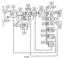
フロント・エンド10のより詳細な説明を、図2に示す。RFフロント・エンド受信器12からのRF処理されたアナログ信号が、A/D変換器14に供給される。ディジタル信号が、サンプリング・レート訂正補間デシメーション・プロセス52に供給される。52の出力は、ディジタルI/Qジェネレータ54に供給され、ディジタルI/Qジェネレータ54は、OFDMデモジュレータ64に必要な複素I成分または複素I信号および複素Q成分または複素Q信号を生成する。複素I/Q信号は、初期粗・シンボル同期化部分56と、ガード・セグメント長デテクタおよび粗周波数オフセット・エスティメータ58に供給される。搬送波周波数オフセットは、周波数オフセット訂正60でI/Q信号を正しくデローテート(de−rotating)することによって、ディジタルに訂正することができる。これは、58の初期粗周波数オフセットを使用する。ガード・セグメント長を、58で検出でき、対応するガード・セグメント期間を、62でI/Q信号ストリームから除去することができる。
A more detailed description of the
ディジタル信号データ・ストリーム(ガード・セグメントなし)が、FFTデモジュレータ64によって処理され、このFFTデモジュレータ64は、複素I/Q信号に対して高速フーリエ周波数変換(FFT)を実行する。2Kモードでは2048ポイント複素FFTが実行され、8Kモードでは8192ポイント複素FFTが実行される。これらは、前に述べた標準規格で使用されるモードである。
The digital signal data stream (without guard segments) is processed by an
複素I/Q成分としての復調されたOFDMシンボルが、TPSデコーダ66、チャネル訂正68、およびチャネル推定70に供給される。チャネル訂正68は、チャネル推定70からの入力も有するが、QAMデマッパ72に出力を供給し、QAMデマッパ72は、受信器バックエンド処理ブロック20に出力を供給する。OFDMデモジュレータ64からのI/Q信号は、SNRエスティメータ74にも供給され、SNRエスティメータ74は、ビタビ・デコーダ76への入力を供給する。復調されたI/Q信号は、ポストFFT周波数オフセット推定78にも供給され、ポストFFT周波数オフセット推定78は、周波数オフセット訂正部分60にフィードバックを供給する。復調されたI/Q信号は、ポストFFTサンプリング・レート・エスティメータ80にも供給され、ポストFFTサンプリング・レート・エスティメータ80は、サンプリング・レート訂正補間デシメーション部分52にフィードバック信号を供給する。復調されたI/Q信号は、ポストFFTシンボル・タイミング推定トラッキング部分82に供給され、ポストFFTシンボル・タイミング推定トラッキング部分82は、ガード期間除去62にフィードバックを供給する。
The demodulated OFDM symbol as a complex I / Q component is provided to a
ポストFFTサンプリング・レート推定回路80が、電圧制御発振器84にも信号を供給し、電圧制御発振器84が、アナログ受信器回路12の最終LO周波数の調整のためにRF受信器12に、およびA/Dサンプリング・レートの調整のためにA/D変換器14に信号を供給することに留意されたい。
A post-FFT sampling rate estimation circuit 80 also provides a signal to the voltage-controlled oscillator 84, which in turn adjusts the
54での複素I/Q信号のディジタル生成は、計算の複雑さおよび受信器に必要な高いMIPsをもたらす。 Digital generation of complex I / Q signals at 54 results in computational complexity and the high MIPs required for the receiver.
本開示では、下で注記するように、初期シンボル同期化、ガード長デテクタ、および初期粗周波数オフセット推定に必要な初期化フェーズ中のディジタル複素I/Q信号生成だけを使用する。その後、OFDMデモジュレータ64の動作が、ディジタルI/Qジェネレータ54なしで必要な復調された複素I/Q成分を作る形で実行される。
In this disclosure, as noted below, only the initial symbol synchronization, guard length detector, and digital complex I / Q signal generation during the initialization phase required for initial coarse frequency offset estimation are used. Thereafter, the operation of the
変更されたOFDMフロント・エンド信号処理アーキテクチャを、図3に示す。受信器は、受信されたOFDMシンボルごとに2*N実数入力FFT(2KモードでN=2048、8KモードでN=8192)を実行する。さらに、受信器は、処理ごとに2つのOFDMシンボルを処理することができ、その結果、1つの2*N複素入力FFTを犠牲にして2つの2*N実数入力FFTを計算できるようになる。図2の従来のDVBT OFDMフロント・エンド信号処理アーキテクチャと比較して、図3の本アーキテクチャは、FFT復調の前のすべてのMIP集中型処理を、初期化の後に不必要にする。 A modified OFDM front end signal processing architecture is shown in FIG. The receiver performs 2 * N real input FFT (N = 2048 in 2K mode, N = 8192 in 8K mode) for each received OFDM symbol. Furthermore, the receiver can process two OFDM symbols per process, so that it can calculate two 2 * N real input FFTs at the expense of one 2 * N complex input FFT. Compared to the conventional DVBT OFDM front end signal processing architecture of FIG. 2, the present architecture of FIG. 3 makes all MIP intensive processing prior to FFT demodulation unnecessary after initialization.
ディジタルI/Q生成が、当初は、初期粗シンボル同期化ブロック56およびガード長検出/粗分数搬送波周波数オフセット推定ブロック58に必要であるが、これは、本発明のすべてのソフトウェアDVBT受信器の初期スタートアップで1回だけ実行され、初期化の後には、ディジタル信号プロセッサMIPリソース全体が、使用のために利用可能になる。
Digital I / Q generation is initially required for the initial coarse
DVBT信号は、約7.61MHzの帯域幅を占める。中央搬送波に変調された信号は、DVB標準規格で定義されているように実数である。しかし、ベースバンドDVBT信号には複素表現が必要である。これは、DVBTベースバンド・スペクトルが、中央周波数をはさんで対称ではないという事実に起因する。これが、従来のDVBT受信器でI/Q複素信号を生成するのにMIP集中型前処理が必要な理由である。しかし、DVBT信号が、FFT入力の通過帯域内に保たれる場合に、FFT入力を実数にすることができ、その結果、I/Q生成が不要になる。 The DVBT signal occupies a bandwidth of about 7.61 MHz. The signal modulated on the center carrier is a real number as defined in the DVB standard. However, the baseband DVBT signal requires a complex representation. This is due to the fact that the DVBT baseband spectrum is not symmetrical across the center frequency. This is the reason why MIP centralized preprocessing is required to generate an I / Q complex signal in a conventional DVBT receiver. However, when the DVBT signal is kept within the pass band of the FFT input, the FFT input can be made a real number, and as a result, I / Q generation becomes unnecessary.
さらに、最終ステージLOおよびA/Dサンプリング・レートは、従来のDVBT受信器で時々必要になる高価な補間およびデシメーションを避けるために、注意深く選択されなければならない。2Kモードでは、搬送波間隔がf=4464Hzであり、サンプリング・レートfsが、正確に2*2048*f=18.284544MHzでなければならない。最終LO周波数f_LOは、正確にfs=4*f_LOとしてセットされなければならない。 Furthermore, the final stage LO and A / D sampling rate must be carefully selected to avoid expensive interpolation and decimation that is sometimes required with conventional DVBT receivers. In 2K mode, the carrier spacing must be f = 4464 Hz and the sampling rate fs must be exactly 2 * 2048 * f = 18.284544 MHz. The final LO frequency f_LO must be set exactly as fs = 4 * f_LO.
4Kモードでは、搬送波間隔がf=2232Hzであり、サンプリング・レートfsは、正確に2*4096*f=18.284544MHzでなければならない。最終LO周波数f_LOは、正確にfs=4*f_LOとしてセットされなければならない。 In 4K mode, the carrier spacing is f = 2232 Hz and the sampling rate fs must be exactly 2 * 4096 * f = 18.284544 MHz. The final LO frequency f_LO must be set exactly as fs = 4 * f_LO.
上のサンプリング・レートfsおよび最終LO周波数のセッティングは、8Kモードについても働かなければならない。というのは、搬送波間隔がf=1116Hzであり、サンプリング・レートfsを正確に2*8192*f=18.284544MHzにしなければならず、最終LO周波数をfs=4*f_LOにしなければならないからである。 The above sampling rate fs and final LO frequency settings must also work for the 8K mode. This is because the carrier spacing is f = 1116 Hz, the sampling rate fs must be exactly 2 * 8192 * f = 18.284544 MHz, and the final LO frequency must be fs = 4 * f_LO. is there.
図3の要素は、図2の要素と同一の機能または関連する機能を有する。受信器12からのアナログ信号が、A/D変換器14に供給される。A/D変換器14の出力が、ディジタルI/Qジェネレータ54ならびにガード期間除去62に供給される。これによって、図3が図2から区別され、ここで、ガード期間除去セクション62は、周波数オフセット訂正の後のディジタル生成されたI/Q信号を受け取る。このディジタルI/Q信号は、初期粗シンボル同期化部分56ならびにガード長デテクタおよび粗周波数オフセット・エスティメータ58に供給される。デテクタおよび初期粗周波数オフセット推定58は、ガード期間除去セクション62に供給される。
The elements of FIG. 3 have the same or related functions as the elements of FIG. An analog signal from the
ガード期間除去62の出力は、ディジタル・ストリームであり、OFDM FFTデモジュレータ64に供給される。図2から区別されるように、これは、I/Q複素シンボルではなく、単に、ガード期間なしのディジタル信号データ・ストリームである。図3では、前に述べたように、OFDMデモジュレータ64が、一時に2つのシンボルを処理し、複素I/Q成分を(ディジタルI/Q生成54なしで)作る。
The output of the
これらのI/Q成分が、TPSデコーダ66、チャネル訂正68、チャネル推定70、SNR推定74、ポストFFT周波数オフセット推定78、およびポストFFTシンボル・タイミング推定トラッキング82に供給される。図2と同様に、チャネル訂正68は、チャネル推定70からも信号を受け取り、入力をQAMデマッパ72に供給する。SNR推定74は、ビタビ・デコーダ76に入力を供給する。ポストFFT周波数オフセット推定78は、電圧制御発振器VCXO 84にフィードバック信号を供給し、電圧制御発振器VCXO 84は、サンプリング・レート信号をA/D変換器14に、フィードバック信号をRF受信器12に供給する。電圧制御発振器84は、初期粗周波数オフセット・エスティメータ58から初期周波数オフセット推定も受け取る。ポストFFTシンボル・タイミング推定トラッキング82は、図2と同様にガード期間除去部分62にフィードバック信号を供給する。
These I / Q components are provided to a
初期粗シンボル同期化部分56ならびにガード長デテクタおよび初期粗周波数オフセット推定58は、図2と同様に初期化中だけに実行されるが、ディジタルI/Q生成54も、初期化ステージ中だけに実行される。I/Qまたはデモジュレータ54、ガード・セグメント長デテクタおよび初期粗周波数オフセット推定58、初期粗シンボル同期化56、ガード期間除去62、ならびにOFDMデモジュレータのすべてが、ソフトウェアで実行されることに留意されたい。
Initial coarse
図4に、OFDMシンボルがA/D入力信号データ・ストリームからどのように抽出されるかを示す。fsでのA/D入力データ・ストリーム・サンプリングが、rx_inと呼ばれるバッファに保管されるものとする。rx_inを保持するバッファは、すべての可能なガード長を含む、3つ以上のOFDMシンボル分のデータ・サンプルを保持するのに十分に大きいものでなければならない。rx_in読み取りポインタrx_in_rdは、シンボル同期化アルゴリズムによって制御され、現在のOFDMシンボルの開始位置をポイントしなければならない。図4に示されているように、2つの2Nポイントが、シンボル1およびシンボル2について入力信号ストリームから抽出される。1つの複素入力FFTを犠牲にして、2つの2Nポイント実数入力FFTを実行できることが周知である。2つのOFDMシンボルを一時に処理して、I/Qデモジュレータ/ジェネレータ部分54が必要とする集中型処理なしでI/Qを作る。
FIG. 4 shows how OFDM symbols are extracted from the A / D input signal data stream. Assume that the A / D input data stream sampling at fs is stored in a buffer called rx_in. The buffer holding rx_in must be large enough to hold three or more OFDM symbol data samples, including all possible guard lengths. The rx_in read pointer rx_in_rd is controlled by the symbol synchronization algorithm and must point to the start position of the current OFDM symbol. As shown in FIG. 4, two 2N points are extracted from the input signal stream for symbol 1 and
より多くの受信器パスを追加することによるSISOの拡張としてのMIMOOFDM受信器を、図5に示す。各受信器パスは、RFアンテナ11アンテナおよびアナログ・フロント・エンド回路の別々のセットと必要な計算の量に応じて同一のまたは別々のサイド・バンド・ディジタル信号プロセッサ内の別々の信号処理チャネルとを必要とする。複数のフロント・エンド信号処理ブロック10からのフロント・エンド処理された信号が、90で組み合わされ、単一の入力としてバックエンド信号処理ブロック20に供給される。各受信器信号処理チャネルは、別々のタイミング同期化、周波数オフセット推定、訂正、およびチャネル推定を実行しなければならない。図1〜3のSISO DVB−T受信器は、レイリ・フェージングとしてモデル化できるNLOS(No−Line Of Sight)ラジオ・チャネルの存在下では不完全に実行する。図5のMIMO−OFDM受信器のSNR/BER改善は、複数の受信器ブランチからの受信信号をコヒーレントに組み合わせることによって得られる。
A MIMO OFDM receiver as an extension of SISO by adding more receiver paths is shown in FIG. Each receiver path has a separate set of
図6に、受信器空間ダイバーシチを有するMIMO−OFDM受信器の性能改善を示す。シミュレーションには、ETSI EN 300 744 V1.4.1(2001−01)に準拠する、64 QAMモード、レート1/2、およびポータブル・レイリ・フェージング・チャネル・モデルをセットした。このプロットは、2つ、3つ、および4つの受信器アンテナからのSNR(DVB−T受信器がQEF条件を達成できる時の)改善を示す。一般的に言って、より多くのアンテナは、受信器複雑さの増加を犠牲にして、よりよいSNR改善をもたらす。 FIG. 6 shows the performance improvement of a MIMO-OFDM receiver with receiver space diversity. The simulation was set up with a 64 QAM mode, rate 1/2, and portable Rayleigh fading channel model according to ETSI EN 300 744 V1.4.1 (2001-01). This plot shows the SNR improvement (when the DVB-T receiver can achieve the QEF condition) from 2, 3, and 4 receiver antennas. Generally speaking, more antennas provide better SNR improvement at the expense of increased receiver complexity.
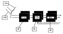
図6に示された性能から、第2の受信器を追加することによって、利得が2.3dB増えるが、3つの受信器を追加することによって、Riceanチャネル・フェージングの場合に利得が5.2dB増える。3つ以上の受信器を追加すると、関連する増加したコストの他に、もう1つ望ましくない現象すなわち、アンテナの相互結合も生じる。アンテナの結合を解除するためには、結合解除ネットワークをフロント・エンドに追加する必要がある。したがって、より多くのチャネルを追加することによって達成される利得は、主に追加の挿入損失によって失われる。よい妥協は、図7および8に示されている、相互に直交するアンテナを有する受信器だけを使用することである。 From the performance shown in FIG. 6, adding a second receiver increases the gain by 2.3 dB, but adding three receivers increases the gain in the case of Rician channel fading to 5.2 dB. Increase. The addition of more than two receivers also causes another undesirable phenomenon, namely antenna mutual coupling, in addition to the associated increased cost. To decouple the antenna, it is necessary to add a decoupling network to the front end. Thus, the gain achieved by adding more channels is lost mainly due to the additional insertion loss. A good compromise is to use only receivers with mutually orthogonal antennas as shown in FIGS.
図7では、アンテナ11Aおよび11Bから来るRF信号が、ブースタ92によって増幅され、その後、ディジタル信号プロセッサによって制御される位相シフタ94に供給される。位相シフタ94は、ディジタル信号プロセッサによって決定される角度だけ、着信波形をシフトし、2つのアンテナからの信号がコヒーレントに組み合わされるようにする。位相シフトされた信号は、整合回路96を介してA/D変換器14に供給される。
In FIG. 7, the RF signals coming from
図8に、ハンドヘルド・デバイス100での2つのアンテナ11Aおよび11Bの配置を示す。これらのアンテナは、直交して位置決めされる。
FIG. 8 shows the arrangement of two
本開示を詳細に説明し、図示したが、これが例示としてのみ行われ、制限と解釈されてはならないことを明瞭に理解されたい。本開示の範囲は、添付請求項の言葉だけによって制限される。 Although the present disclosure has been described and illustrated in detail, it should be clearly understood that this is done by way of example only and should not be construed as limiting. The scope of the present disclosure is limited only by the language of the appended claims.
Claims (11)
前記ディジタル信号データ・ストリームから複素I成分および複素Q成分の第1セットを作るI/Qデモジュレータと、
I成分およびQ成分の前記第1セットを使用するガード・セグメント長デテクタと、
前記ディジタル信号データ・ストリームから前記検出された長さの前記ガード・セグメントを識別し、除去するエクストラクタと、
複素I成分および複素Q成分の第2セットを作るために、前記ディジタル信号データ・ストリームの前記シンボルを復調するFFTデモジュレータと
を含む受信器。 An A / D converter for converting a received analog signal into a digital signal data stream, wherein the digital signal data stream includes symbols separated by guard segments;
An I / Q demodulator for creating a first set of complex I and Q components from the digital signal data stream;
A guard segment length detector using the first set of I and Q components;
An extractor for identifying and removing the guard segment of the detected length from the digital signal data stream;
An FFT demodulator that demodulates the symbols of the digital signal data stream to produce a second set of complex I and Q components.
Applications Claiming Priority (2)
| Application Number | Priority Date | Filing Date | Title |
|---|---|---|---|
| US57760204P | 2004-06-08 | 2004-06-08 | |
| PCT/US2005/019814 WO2005125136A1 (en) | 2004-06-08 | 2005-06-07 | Orthogonal frequency division multiplexing receiver |
Publications (2)
| Publication Number | Publication Date |
|---|---|
| JP2008502282A true JP2008502282A (en) | 2008-01-24 |
| JP2008502282A5 JP2008502282A5 (en) | 2008-04-03 |
Family
ID=35510109
Family Applications (1)
| Application Number | Title | Priority Date | Filing Date |
|---|---|---|---|
| JP2007527622A Withdrawn JP2008502282A (en) | 2004-06-08 | 2005-06-07 | Orthogonal frequency division multiplex receiver |
Country Status (5)
| Country | Link |
|---|---|
| US (1) | US7346114B2 (en) |
| EP (1) | EP1754355A1 (en) |
| JP (1) | JP2008502282A (en) |
| CN (1) | CN1860753A (en) |
| WO (1) | WO2005125136A1 (en) |
Families Citing this family (14)
| Publication number | Priority date | Publication date | Assignee | Title |
|---|---|---|---|---|
| US7952511B1 (en) | 1999-04-07 | 2011-05-31 | Geer James L | Method and apparatus for the detection of objects using electromagnetic wave attenuation patterns |
| US7643549B2 (en) * | 2004-09-28 | 2010-01-05 | Broadcom Corporation | Wireless device having a hardware accelerator to support equalization processing |
| US7765086B2 (en) * | 2004-12-09 | 2010-07-27 | Tektronix, Inc. | Modulation domain trigger |
| WO2007103099A1 (en) * | 2006-03-07 | 2007-09-13 | Interdigital Technology Corporation | Method and apparatus for correcting sample clock frequency offset in ofdm mimo systems |
| US7676207B2 (en) * | 2006-03-08 | 2010-03-09 | Newport Media, Inc. | System and method for digital autonomous automatic gain control (AGC) for DVB-H receivers |
| CN101455008B (en) * | 2006-04-03 | 2012-10-24 | 伟俄内克斯研究公司 | Frequency offset correction for an ultrawideband communication system |
| US7881398B2 (en) * | 2006-08-21 | 2011-02-01 | Agere Systems Inc. | FFT numerology for an OFDM transmission system |
| CN104113504A (en) * | 2007-03-29 | 2014-10-22 | 深圳赛意法微电子有限公司 | DRM receiver with analog and digital separation filter and demodulation method |
| US8174958B2 (en) * | 2008-08-01 | 2012-05-08 | Broadcom Corporation | Method and system for a reference signal (RS) timing loop for OFDM symbol synchronization and tracking |
| US8559296B2 (en) | 2008-08-01 | 2013-10-15 | Broadcom Corporation | Method and system for an OFDM joint timing and frequency tracking system |
| CN101969574B (en) * | 2009-05-20 | 2013-08-07 | 晨星软件研发(深圳)有限公司 | Circuit for detecting a digital data stream and associated method |
| GB2478143A (en) * | 2010-02-25 | 2011-08-31 | Sony Corp | Selective local data insertion using hierarchical modulation symbols on OFDM sub-carriers in DVB-NGH system |
| US9124396B2 (en) * | 2011-07-28 | 2015-09-01 | Allen LeRoy Limberg | COFDM digital television receivers for iterative-diversity reception |
| US8767855B2 (en) * | 2012-04-07 | 2014-07-01 | Greenvity Communications, Inc. | Method of estimating sampling clock offset, a sampling clock offset estimator and a receiver comprising the same |
Family Cites Families (12)
| Publication number | Priority date | Publication date | Assignee | Title |
|---|---|---|---|---|
| DE4240226C2 (en) | 1992-11-30 | 1996-12-12 | Deutsche Forsch Luft Raumfahrt | Process for the digital transmission of hierarchical HDTV, EDTV and SDTV television signals |
| JP3289610B2 (en) | 1996-07-31 | 2002-06-10 | 日本ビクター株式会社 | OFDM demodulator and method |
| US6359938B1 (en) | 1996-10-31 | 2002-03-19 | Discovision Associates | Single chip VLSI implementation of a digital receiver employing orthogonal frequency division multiplexing |
| TW465234B (en) | 1997-02-18 | 2001-11-21 | Discovision Ass | Single chip VLSI implementation of a digital receiver employing orthogonal frequency division multiplexing |
| US6005894A (en) | 1997-04-04 | 1999-12-21 | Kumar; Derek D. | AM-compatible digital broadcasting method and system |
| US6320917B1 (en) | 1997-05-02 | 2001-11-20 | Lsi Logic Corporation | Demodulating digital video broadcast signals |
| US6240146B1 (en) | 1997-05-02 | 2001-05-29 | Lsi Logic Corporation | Demodulating digital video broadcast signals |
| US6317470B1 (en) | 1998-09-15 | 2001-11-13 | Ibiquity Digital Corporation | Adaptive weighting method for orthogonal frequency division multiplexed soft symbols using channel state information estimates |
| GB2364865B (en) * | 2000-07-12 | 2004-01-21 | Conexant Systems Inc | Receiver circuit |
| JP2004112216A (en) * | 2002-09-17 | 2004-04-08 | Alps Electric Co Ltd | Ofdm receiver |
| JP4302410B2 (en) * | 2003-02-28 | 2009-07-29 | 独立行政法人情報通信研究機構 | Receiving device, receiving method, and program |
| KR100510549B1 (en) | 2003-09-26 | 2005-08-26 | 삼성전자주식회사 | Channel state measurement apparatus providing for detecting and suppressing of co-channel interference in digital video broadcasting receiver and method therefor |
-
2005
- 2005-06-07 US US10/574,585 patent/US7346114B2/en not_active Expired - Fee Related
- 2005-06-07 CN CNA2005800010036A patent/CN1860753A/en active Pending
- 2005-06-07 JP JP2007527622A patent/JP2008502282A/en not_active Withdrawn
- 2005-06-07 EP EP05757666A patent/EP1754355A1/en not_active Withdrawn
- 2005-06-07 WO PCT/US2005/019814 patent/WO2005125136A1/en not_active Application Discontinuation
Also Published As
| Publication number | Publication date |
|---|---|
| US20070183514A1 (en) | 2007-08-09 |
| WO2005125136A1 (en) | 2005-12-29 |
| CN1860753A (en) | 2006-11-08 |
| EP1754355A1 (en) | 2007-02-21 |
| US7346114B2 (en) | 2008-03-18 |
Similar Documents
| Publication | Publication Date | Title |
|---|---|---|
| US7346114B2 (en) | Receiver with signal offset estimator and symbol synchronizing generator | |
| KR101165873B1 (en) | Tps decoder in an orthogonal frequency division multiplexing receiver | |
| RU2450472C1 (en) | Synchronisation of ofdm symbols using preamble with frequency-shifted prefix and suffix for dvr-t2 receiver | |
| US8270502B2 (en) | Timing-frequency offset and carrier-frequency offset estimations for multi-carrier modulated signals using pilot tones | |
| JP2004032748A (en) | Multipath equalizing technique for orthogonal frequency division multiplexing communication system | |
| US9912456B2 (en) | Method and apparatus for transmitting a-priori information in a communication system | |
| US8781421B2 (en) | Time-domain diversity combining of signals for broadcast receivers | |
| KR101514099B1 (en) | Method and apparatus for signal discovery | |
| KR101395686B1 (en) | Apparatus and method for removing common phase error in a dvb-t/h receiver | |
| JP4317335B2 (en) | Diversity receiver | |
| KR101406160B1 (en) | Apparatus and method for removing common phase error in a dvb-t/h receiver | |
| US20120321021A1 (en) | Ofdm reception device, ofdm reception circuit, ofdm reception method, and ofdm reception program | |
| US9118533B2 (en) | Antenna diversity combining for differentially modulated orthogonal frequency division multiplexed (OFDM) signals | |
| JP2007208856A (en) | Ofdm demodulation apparatus, method of operating ofdm demodulation apparatus, program, and computer-readable recording medium | |
| KR20070020390A (en) | Orthogonal frequency division multiplexing receiver | |
| JP2005136471A (en) | Ofdm receiver using diversity, ofdm reception circuit using diversity, and ofdm reception method using diversity | |
| RU2577316C2 (en) | Signal processing device, signal processing method and programme | |
| US8699632B2 (en) | OFDM reception device, OFDM reception circuit, OFDM reception method, and OFDM reception program | |
| US10911289B1 (en) | Interface to provide selectable time domain or frequency domain information to downstream circuitry | |
| KR100860460B1 (en) | DSP apparatus and method in OFDM receiver using antenna diversity technique | |
| KR101011261B1 (en) | Apparatus and method for receiving in DMB | |
| JP2009212835A (en) | Ofdm receiver | |
| JP2009153220A (en) | Centralized buffer architecture for orthogonal frequency division multiplexing (ofdm) receiver |
Legal Events
| Date | Code | Title | Description |
|---|---|---|---|
| A521 | Request for written amendment filed |
Free format text: JAPANESE INTERMEDIATE CODE: A523 Effective date: 20080212 |
|
| A621 | Written request for application examination |
Free format text: JAPANESE INTERMEDIATE CODE: A621 Effective date: 20080212 |
|
| A761 | Written withdrawal of application |
Free format text: JAPANESE INTERMEDIATE CODE: A761 Effective date: 20081128 |