JP2008502150A - Improved dual damascene integrated structure and method of manufacturing the same - Google Patents
Improved dual damascene integrated structure and method of manufacturing the same Download PDFInfo
- Publication number
- JP2008502150A JP2008502150A JP2007515542A JP2007515542A JP2008502150A JP 2008502150 A JP2008502150 A JP 2008502150A JP 2007515542 A JP2007515542 A JP 2007515542A JP 2007515542 A JP2007515542 A JP 2007515542A JP 2008502150 A JP2008502150 A JP 2008502150A
- Authority
- JP
- Japan
- Prior art keywords
- layer
- gas cluster
- hard mask
- ion beam
- cluster ion
- Prior art date
- Legal status (The legal status is an assumption and is not a legal conclusion. Google has not performed a legal analysis and makes no representation as to the accuracy of the status listed.)
- Withdrawn
Links
- 230000009977 dual effect Effects 0.000 title claims abstract description 16
- 238000004519 manufacturing process Methods 0.000 title claims description 8
- 238000000034 method Methods 0.000 claims abstract description 118
- 239000000463 material Substances 0.000 claims abstract description 67
- 230000008569 process Effects 0.000 claims abstract description 63
- 238000005530 etching Methods 0.000 claims abstract description 51
- 238000010884 ion-beam technique Methods 0.000 claims abstract description 32
- 238000000280 densification Methods 0.000 claims abstract description 8
- 239000007789 gas Substances 0.000 claims description 96
- 229920002120 photoresistant polymer Polymers 0.000 claims description 40
- 230000000873 masking effect Effects 0.000 claims description 30
- 238000001020 plasma etching Methods 0.000 claims description 28
- 150000002500 ions Chemical class 0.000 claims description 21
- XKRFYHLGVUSROY-UHFFFAOYSA-N Argon Chemical compound [Ar] XKRFYHLGVUSROY-UHFFFAOYSA-N 0.000 claims description 18
- 239000011810 insulating material Substances 0.000 claims description 16
- QVGXLLKOCUKJST-UHFFFAOYSA-N atomic oxygen Chemical compound [O] QVGXLLKOCUKJST-UHFFFAOYSA-N 0.000 claims description 15
- 239000001301 oxygen Substances 0.000 claims description 15
- 229910052760 oxygen Inorganic materials 0.000 claims description 15
- IJGRMHOSHXDMSA-UHFFFAOYSA-N Atomic nitrogen Chemical compound N#N IJGRMHOSHXDMSA-UHFFFAOYSA-N 0.000 claims description 14
- 239000006117 anti-reflective coating Substances 0.000 claims description 12
- 239000000758 substrate Substances 0.000 claims description 11
- 229910004298 SiO 2 Inorganic materials 0.000 claims description 10
- 229910052786 argon Inorganic materials 0.000 claims description 9
- 229910052757 nitrogen Inorganic materials 0.000 claims description 7
- 239000004065 semiconductor Substances 0.000 claims description 7
- 238000012546 transfer Methods 0.000 claims description 7
- 239000001257 hydrogen Substances 0.000 claims description 3
- 229910052739 hydrogen Inorganic materials 0.000 claims description 3
- 238000003672 processing method Methods 0.000 claims description 3
- 238000011049 filling Methods 0.000 claims description 2
- VNWKTOKETHGBQD-UHFFFAOYSA-N methane Chemical compound C VNWKTOKETHGBQD-UHFFFAOYSA-N 0.000 claims 8
- PXGOKWXKJXAPGV-UHFFFAOYSA-N Fluorine Chemical compound FF PXGOKWXKJXAPGV-UHFFFAOYSA-N 0.000 claims 2
- UFHFLCQGNIYNRP-UHFFFAOYSA-N Hydrogen Chemical compound [H][H] UFHFLCQGNIYNRP-UHFFFAOYSA-N 0.000 claims 2
- 239000011737 fluorine Substances 0.000 claims 2
- 229910052731 fluorine Inorganic materials 0.000 claims 2
- 239000001307 helium Substances 0.000 claims 2
- 229910052734 helium Inorganic materials 0.000 claims 2
- SWQJXJOGLNCZEY-UHFFFAOYSA-N helium atom Chemical compound [He] SWQJXJOGLNCZEY-UHFFFAOYSA-N 0.000 claims 2
- 230000001678 irradiating effect Effects 0.000 claims 2
- 239000011148 porous material Substances 0.000 claims 1
- 238000012545 processing Methods 0.000 abstract description 41
- 238000004380 ashing Methods 0.000 abstract description 14
- 239000012212 insulator Substances 0.000 abstract description 13
- 238000007789 sealing Methods 0.000 abstract description 7
- 239000010410 layer Substances 0.000 description 135
- 230000015572 biosynthetic process Effects 0.000 description 20
- 238000010586 diagram Methods 0.000 description 15
- 230000000694 effects Effects 0.000 description 12
- 239000000203 mixture Substances 0.000 description 9
- RYGMFSIKBFXOCR-UHFFFAOYSA-N Copper Chemical compound [Cu] RYGMFSIKBFXOCR-UHFFFAOYSA-N 0.000 description 8
- 229910052802 copper Inorganic materials 0.000 description 8
- 239000010949 copper Substances 0.000 description 8
- 230000010354 integration Effects 0.000 description 8
- 238000011282 treatment Methods 0.000 description 8
- 230000004888 barrier function Effects 0.000 description 6
- 238000000151 deposition Methods 0.000 description 6
- 230000008021 deposition Effects 0.000 description 6
- 239000002184 metal Substances 0.000 description 6
- 229910052751 metal Inorganic materials 0.000 description 6
- 238000000231 atomic layer deposition Methods 0.000 description 5
- 238000005229 chemical vapour deposition Methods 0.000 description 5
- 238000011109 contamination Methods 0.000 description 5
- 239000000126 substance Substances 0.000 description 4
- 125000004429 atom Chemical group 0.000 description 3
- 230000032798 delamination Effects 0.000 description 3
- 238000009499 grossing Methods 0.000 description 3
- 230000006872 improvement Effects 0.000 description 3
- 239000013077 target material Substances 0.000 description 3
- CURLTUGMZLYLDI-UHFFFAOYSA-N Carbon dioxide Chemical compound O=C=O CURLTUGMZLYLDI-UHFFFAOYSA-N 0.000 description 2
- 230000001133 acceleration Effects 0.000 description 2
- 230000003667 anti-reflective effect Effects 0.000 description 2
- 239000003963 antioxidant agent Substances 0.000 description 2
- 230000003078 antioxidant effect Effects 0.000 description 2
- 238000006243 chemical reaction Methods 0.000 description 2
- 238000013461 design Methods 0.000 description 2
- 238000000605 extraction Methods 0.000 description 2
- 239000000178 monomer Substances 0.000 description 2
- 239000011265 semifinished product Substances 0.000 description 2
- 239000002904 solvent Substances 0.000 description 2
- 238000004381 surface treatment Methods 0.000 description 2
- 241000233805 Phoenix Species 0.000 description 1
- 230000003064 anti-oxidating effect Effects 0.000 description 1
- 239000001569 carbon dioxide Substances 0.000 description 1
- 229910002092 carbon dioxide Inorganic materials 0.000 description 1
- 150000001793 charged compounds Chemical class 0.000 description 1
- 238000004140 cleaning Methods 0.000 description 1
- 239000004020 conductor Substances 0.000 description 1
- 238000007796 conventional method Methods 0.000 description 1
- 238000009792 diffusion process Methods 0.000 description 1
- 239000006185 dispersion Substances 0.000 description 1
- 239000002305 electric material Substances 0.000 description 1
- 238000005516 engineering process Methods 0.000 description 1
- 239000000284 extract Substances 0.000 description 1
- 125000004435 hydrogen atom Chemical class [H]* 0.000 description 1
- 230000003116 impacting effect Effects 0.000 description 1
- 238000009413 insulation Methods 0.000 description 1
- WABPQHHGFIMREM-RKEGKUSMSA-N lead-214 Chemical compound [214Pb] WABPQHHGFIMREM-RKEGKUSMSA-N 0.000 description 1
- 238000011068 loading method Methods 0.000 description 1
- 238000012986 modification Methods 0.000 description 1
- 230000004048 modification Effects 0.000 description 1
- 230000002093 peripheral effect Effects 0.000 description 1
- 238000000206 photolithography Methods 0.000 description 1
- 238000005498 polishing Methods 0.000 description 1
- 229920000642 polymer Polymers 0.000 description 1
- 239000000047 product Substances 0.000 description 1
- 239000002356 single layer Substances 0.000 description 1
- 238000003860 storage Methods 0.000 description 1
Images


Classifications
-
- H—ELECTRICITY
- H01—ELECTRIC ELEMENTS
- H01L—SEMICONDUCTOR DEVICES NOT COVERED BY CLASS H10
- H01L21/00—Processes or apparatus adapted for the manufacture or treatment of semiconductor or solid state devices or of parts thereof
- H01L21/02—Manufacture or treatment of semiconductor devices or of parts thereof
- H01L21/04—Manufacture or treatment of semiconductor devices or of parts thereof the devices having potential barriers, e.g. a PN junction, depletion layer or carrier concentration layer
- H01L21/18—Manufacture or treatment of semiconductor devices or of parts thereof the devices having potential barriers, e.g. a PN junction, depletion layer or carrier concentration layer the devices having semiconductor bodies comprising elements of Group IV of the Periodic Table or AIIIBV compounds with or without impurities, e.g. doping materials
- H01L21/30—Treatment of semiconductor bodies using processes or apparatus not provided for in groups H01L21/20 - H01L21/26
- H01L21/31—Treatment of semiconductor bodies using processes or apparatus not provided for in groups H01L21/20 - H01L21/26 to form insulating layers thereon, e.g. for masking or by using photolithographic techniques; After treatment of these layers; Selection of materials for these layers
- H01L21/3105—After-treatment
- H01L21/311—Etching the insulating layers by chemical or physical means
- H01L21/31144—Etching the insulating layers by chemical or physical means using masks
-
- H—ELECTRICITY
- H01—ELECTRIC ELEMENTS
- H01L—SEMICONDUCTOR DEVICES NOT COVERED BY CLASS H10
- H01L21/00—Processes or apparatus adapted for the manufacture or treatment of semiconductor or solid state devices or of parts thereof
- H01L21/02—Manufacture or treatment of semiconductor devices or of parts thereof
- H01L21/04—Manufacture or treatment of semiconductor devices or of parts thereof the devices having potential barriers, e.g. a PN junction, depletion layer or carrier concentration layer
- H01L21/18—Manufacture or treatment of semiconductor devices or of parts thereof the devices having potential barriers, e.g. a PN junction, depletion layer or carrier concentration layer the devices having semiconductor bodies comprising elements of Group IV of the Periodic Table or AIIIBV compounds with or without impurities, e.g. doping materials
- H01L21/30—Treatment of semiconductor bodies using processes or apparatus not provided for in groups H01L21/20 - H01L21/26
- H01L21/31—Treatment of semiconductor bodies using processes or apparatus not provided for in groups H01L21/20 - H01L21/26 to form insulating layers thereon, e.g. for masking or by using photolithographic techniques; After treatment of these layers; Selection of materials for these layers
- H01L21/3105—After-treatment
- H01L21/311—Etching the insulating layers by chemical or physical means
- H01L21/31105—Etching inorganic layers
- H01L21/31111—Etching inorganic layers by chemical means
- H01L21/31116—Etching inorganic layers by chemical means by dry-etching
-
- H—ELECTRICITY
- H01—ELECTRIC ELEMENTS
- H01L—SEMICONDUCTOR DEVICES NOT COVERED BY CLASS H10
- H01L21/00—Processes or apparatus adapted for the manufacture or treatment of semiconductor or solid state devices or of parts thereof
- H01L21/02—Manufacture or treatment of semiconductor devices or of parts thereof
- H01L21/04—Manufacture or treatment of semiconductor devices or of parts thereof the devices having potential barriers, e.g. a PN junction, depletion layer or carrier concentration layer
- H01L21/18—Manufacture or treatment of semiconductor devices or of parts thereof the devices having potential barriers, e.g. a PN junction, depletion layer or carrier concentration layer the devices having semiconductor bodies comprising elements of Group IV of the Periodic Table or AIIIBV compounds with or without impurities, e.g. doping materials
- H01L21/30—Treatment of semiconductor bodies using processes or apparatus not provided for in groups H01L21/20 - H01L21/26
- H01L21/31—Treatment of semiconductor bodies using processes or apparatus not provided for in groups H01L21/20 - H01L21/26 to form insulating layers thereon, e.g. for masking or by using photolithographic techniques; After treatment of these layers; Selection of materials for these layers
- H01L21/3105—After-treatment
- H01L21/311—Etching the insulating layers by chemical or physical means
- H01L21/31127—Etching organic layers
- H01L21/31133—Etching organic layers by chemical means
- H01L21/31138—Etching organic layers by chemical means by dry-etching
-
- H—ELECTRICITY
- H01—ELECTRIC ELEMENTS
- H01L—SEMICONDUCTOR DEVICES NOT COVERED BY CLASS H10
- H01L21/00—Processes or apparatus adapted for the manufacture or treatment of semiconductor or solid state devices or of parts thereof
- H01L21/70—Manufacture or treatment of devices consisting of a plurality of solid state components formed in or on a common substrate or of parts thereof; Manufacture of integrated circuit devices or of parts thereof
- H01L21/71—Manufacture of specific parts of devices defined in group H01L21/70
- H01L21/768—Applying interconnections to be used for carrying current between separate components within a device comprising conductors and dielectrics
- H01L21/76801—Applying interconnections to be used for carrying current between separate components within a device comprising conductors and dielectrics characterised by the formation and the after-treatment of the dielectrics, e.g. smoothing
- H01L21/76802—Applying interconnections to be used for carrying current between separate components within a device comprising conductors and dielectrics characterised by the formation and the after-treatment of the dielectrics, e.g. smoothing by forming openings in dielectrics
- H01L21/76807—Applying interconnections to be used for carrying current between separate components within a device comprising conductors and dielectrics characterised by the formation and the after-treatment of the dielectrics, e.g. smoothing by forming openings in dielectrics for dual damascene structures
- H01L21/76808—Applying interconnections to be used for carrying current between separate components within a device comprising conductors and dielectrics characterised by the formation and the after-treatment of the dielectrics, e.g. smoothing by forming openings in dielectrics for dual damascene structures involving intermediate temporary filling with material
-
- H—ELECTRICITY
- H01—ELECTRIC ELEMENTS
- H01L—SEMICONDUCTOR DEVICES NOT COVERED BY CLASS H10
- H01L21/00—Processes or apparatus adapted for the manufacture or treatment of semiconductor or solid state devices or of parts thereof
- H01L21/70—Manufacture or treatment of devices consisting of a plurality of solid state components formed in or on a common substrate or of parts thereof; Manufacture of integrated circuit devices or of parts thereof
- H01L21/71—Manufacture of specific parts of devices defined in group H01L21/70
- H01L21/768—Applying interconnections to be used for carrying current between separate components within a device comprising conductors and dielectrics
- H01L21/76801—Applying interconnections to be used for carrying current between separate components within a device comprising conductors and dielectrics characterised by the formation and the after-treatment of the dielectrics, e.g. smoothing
- H01L21/76802—Applying interconnections to be used for carrying current between separate components within a device comprising conductors and dielectrics characterised by the formation and the after-treatment of the dielectrics, e.g. smoothing by forming openings in dielectrics
- H01L21/76814—Applying interconnections to be used for carrying current between separate components within a device comprising conductors and dielectrics characterised by the formation and the after-treatment of the dielectrics, e.g. smoothing by forming openings in dielectrics post-treatment or after-treatment, e.g. cleaning or removal of oxides on underlying conductors
-
- H—ELECTRICITY
- H01—ELECTRIC ELEMENTS
- H01L—SEMICONDUCTOR DEVICES NOT COVERED BY CLASS H10
- H01L21/00—Processes or apparatus adapted for the manufacture or treatment of semiconductor or solid state devices or of parts thereof
- H01L21/70—Manufacture or treatment of devices consisting of a plurality of solid state components formed in or on a common substrate or of parts thereof; Manufacture of integrated circuit devices or of parts thereof
- H01L21/71—Manufacture of specific parts of devices defined in group H01L21/70
- H01L21/768—Applying interconnections to be used for carrying current between separate components within a device comprising conductors and dielectrics
- H01L21/76801—Applying interconnections to be used for carrying current between separate components within a device comprising conductors and dielectrics characterised by the formation and the after-treatment of the dielectrics, e.g. smoothing
- H01L21/7682—Applying interconnections to be used for carrying current between separate components within a device comprising conductors and dielectrics characterised by the formation and the after-treatment of the dielectrics, e.g. smoothing the dielectric comprising air gaps
-
- H—ELECTRICITY
- H01—ELECTRIC ELEMENTS
- H01L—SEMICONDUCTOR DEVICES NOT COVERED BY CLASS H10
- H01L21/00—Processes or apparatus adapted for the manufacture or treatment of semiconductor or solid state devices or of parts thereof
- H01L21/70—Manufacture or treatment of devices consisting of a plurality of solid state components formed in or on a common substrate or of parts thereof; Manufacture of integrated circuit devices or of parts thereof
- H01L21/71—Manufacture of specific parts of devices defined in group H01L21/70
- H01L21/768—Applying interconnections to be used for carrying current between separate components within a device comprising conductors and dielectrics
- H01L21/76801—Applying interconnections to be used for carrying current between separate components within a device comprising conductors and dielectrics characterised by the formation and the after-treatment of the dielectrics, e.g. smoothing
- H01L21/76822—Modification of the material of dielectric layers, e.g. grading, after-treatment to improve the stability of the layers, to increase their density etc.
- H01L21/76825—Modification of the material of dielectric layers, e.g. grading, after-treatment to improve the stability of the layers, to increase their density etc. by exposing the layer to particle radiation, e.g. ion implantation, irradiation with UV light or electrons etc.
-
- H—ELECTRICITY
- H01—ELECTRIC ELEMENTS
- H01L—SEMICONDUCTOR DEVICES NOT COVERED BY CLASS H10
- H01L21/00—Processes or apparatus adapted for the manufacture or treatment of semiconductor or solid state devices or of parts thereof
- H01L21/70—Manufacture or treatment of devices consisting of a plurality of solid state components formed in or on a common substrate or of parts thereof; Manufacture of integrated circuit devices or of parts thereof
- H01L21/71—Manufacture of specific parts of devices defined in group H01L21/70
- H01L21/768—Applying interconnections to be used for carrying current between separate components within a device comprising conductors and dielectrics
- H01L21/76801—Applying interconnections to be used for carrying current between separate components within a device comprising conductors and dielectrics characterised by the formation and the after-treatment of the dielectrics, e.g. smoothing
- H01L21/76829—Applying interconnections to be used for carrying current between separate components within a device comprising conductors and dielectrics characterised by the formation and the after-treatment of the dielectrics, e.g. smoothing characterised by the formation of thin functional dielectric layers, e.g. dielectric etch-stop, barrier, capping or liner layers
- H01L21/76831—Applying interconnections to be used for carrying current between separate components within a device comprising conductors and dielectrics characterised by the formation and the after-treatment of the dielectrics, e.g. smoothing characterised by the formation of thin functional dielectric layers, e.g. dielectric etch-stop, barrier, capping or liner layers in via holes or trenches, e.g. non-conductive sidewall liners
-
- H—ELECTRICITY
- H01—ELECTRIC ELEMENTS
- H01J—ELECTRIC DISCHARGE TUBES OR DISCHARGE LAMPS
- H01J2237/00—Discharge tubes exposing object to beam, e.g. for analysis treatment, etching, imaging
- H01J2237/06—Sources
- H01J2237/08—Ion sources
- H01J2237/0812—Ionized cluster beam [ICB] sources
-
- H—ELECTRICITY
- H01—ELECTRIC ELEMENTS
- H01L—SEMICONDUCTOR DEVICES NOT COVERED BY CLASS H10
- H01L21/00—Processes or apparatus adapted for the manufacture or treatment of semiconductor or solid state devices or of parts thereof
- H01L21/02—Manufacture or treatment of semiconductor devices or of parts thereof
- H01L21/02041—Cleaning
- H01L21/02043—Cleaning before device manufacture, i.e. Begin-Of-Line process
- H01L21/02046—Dry cleaning only
Landscapes
- Engineering & Computer Science (AREA)
- Physics & Mathematics (AREA)
- Computer Hardware Design (AREA)
- Condensed Matter Physics & Semiconductors (AREA)
- General Physics & Mathematics (AREA)
- Manufacturing & Machinery (AREA)
- Microelectronics & Electronic Packaging (AREA)
- Power Engineering (AREA)
- Chemical & Material Sciences (AREA)
- Chemical Kinetics & Catalysis (AREA)
- General Chemical & Material Sciences (AREA)
- Plasma & Fusion (AREA)
- Inorganic Chemistry (AREA)
- Internal Circuitry In Semiconductor Integrated Circuit Devices (AREA)
- Drying Of Semiconductors (AREA)
Abstract
ガスクラスターイオンビーム処理を用いた多孔質超低k値(ULK)絶縁体材料内に二重ダマシン構造を形成する方法に関して開示する。これらの方法においては二重ダマシンULK処理中におけるハードマスク層を最小にし、最終的なULK二重ダマシン構造内には、ハードマスク層が存在しない。ガスクラスターイオンビームのエッチング処理、緻密化処理、孔のシーリング処理、アッシング処理の各方法が記載されており、該方法は、材料の除去と同時にULKインターフェースの緻密化を進行させる。緻密なインターフェースとハードマスクがない新規なULK二重ダマシン構造が含まれている。
【選択図】なしDisclosed is a method for forming a dual damascene structure in a porous ultra low k value (ULK) insulator material using gas cluster ion beam processing. These methods minimize the hard mask layer during double damascene ULK processing, and there is no hard mask layer in the final ULK double damascene structure. A gas cluster ion beam etching process, a densification process, a hole sealing process, and an ashing process are described. The method advances the densification of the ULK interface simultaneously with the material removal. A new ULK double damascene structure without a precise interface and hard mask is included.
[Selection figure] None
Description
本発明は、低い誘電率(low dielectric constant (low-k) )の絶縁体を利用した半導体集積回路(semiconductor integrated circuits)のための改善された二重ダマシン集積構造(dual damascene integration structures)および、低いk値(low-k)を有する絶縁体とガスクラスターイオンビーム処理を用いた前記構造の製造方法に関する。 The present invention provides an improved dual damascene integration structure for semiconductor integrated circuits utilizing low dielectric constant (low-k) insulators, and The present invention relates to a method for manufacturing the structure using an insulator having a low k value (low-k) and gas cluster ion beam processing.
半導体産業は、スケーリング(scaling)を用いることによって市場に費用対効果の高いチップ(chips)を供給することにより、すさまじい成功を収めた。スケーリングは装置や半導体プロセッサのフロントエンド(front end)に重要な役割を果たしたが、装置の配線はスケーリングに追随できず、内部抵抗や静電容量(キャパシタンス(capacitance))の低下を招いた。この問題を緩和するために、低抵抗コンダクタ(銅など)を使用したり、低いk値を持つ絶縁体を導入してキャパシタンスの問題を低減した。近年、非常に多孔性(30〜50%)であることによって特徴的な超低k値(ULK;k<2.5)の絶縁体が発展した。これらの材料は他の湿性な化合物やガス(wet chemicals and gases)により汚染されやすいので集積が非常に難しい。 The semiconductor industry has achieved tremendous success by providing cost-effective chips to the market by using scaling. Scaling played an important role in the front end of devices and semiconductor processors, but the wiring of the device could not follow the scaling, leading to a decrease in internal resistance and capacitance. To alleviate this problem, low resistance conductors (such as copper) were used, or insulators with low k values were introduced to reduce capacitance problems. In recent years, insulators with characteristic ultra-low k values (ULK; k <2.5) have evolved due to their very porosity (30-50%). These materials are very difficult to accumulate because they are easily contaminated by other wet chemicals and gases.
通常の二重ダマシン−ULK集積は、多孔性でもろいULKフィルムの表面を高k値ハードマスクフィルムにより保護されて得られる。最も広く利用される二つのプロセスは、“ヴィアファースト(via first)”と通常の“二重ハードマスク”である。 Normal double damascene-ULK integration is obtained by protecting the surface of a porous, brittle ULK film with a high-k hard mask film. The two most widely used processes are “via first” and the usual “double hard mask”.
図2A−2Fは、二重ダマシンULK集積処理のための“ヴィアファースト”の各段階(300A−300F)を示した図である。“ヴィアファースト”処理は、従来の金属配線上に絶縁フィルム連続層を形成するところから始まる(図示していない)。図2Aに示すように、この絶縁堆積層300Aは、エッチングストップフィルム302、ULK絶縁層304、第一ハードマスク層306、第二ハードマスク層308、反射防止膜310、フォトレジスト層312よりなる。エッチングストップフィルム302は、適当な低いk値を有し、ULK絶縁層304は、エッチングストップフィルム302に対して高いエッチ速度を持っている。もし最初(基板)の金属配線層が銅であると、エッチングストップフィルム302は銅の拡散バリアでもある必要がある。この明細書ではエッチングストップフィルムとしてはほとんどSiCN、Si3N4である。
FIGS. 2A-2F are diagrams showing the “via first” stages (300A-300F) for dual damascene ULK integration processing. The “via first” process begins with the formation of a continuous layer of insulating film on a conventional metal wiring (not shown). As shown in FIG. 2A, the
第一ハードマスク層306は、後のケミカルメカニカルポリッシング(chemical mechanical polishing (CMP))工程の効果から、もろくて多孔性のULK絶縁層304を保護するするために二重ダマシン構造の一部として残される。第二ハードマスク層308は、抗酸化性を有し、フォトリワーク工程で反射防止膜310およびフォトレジスト312の除去ができるような材料である。典型的な材料としては、第一ハードマスク層306はSiCOH、SiCが、第二ハードマスク層308にはSiO2、、Si3N4が用いられる。第二ハードマスク層308は、犠牲層であり、銅およびバリア材料がCMPの間に除去されるである。
The first
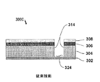
図2Bの300Bの構造は、フォトレジスト層312に所望のヴィアパターンが描かれ、反応イオンエッチング(RIE)によりそのパターンが反射防止膜310と、ハードマスク層306および308と、ULK絶縁層304を通してSiCNエッチングストップまで転写し、ヴィア324が形成された状態である。図2Cは酸素その他の混合ガスのプラズマアッシング(plasma ashing)により残ったフォトレジスト層312と反射防止膜310が除去され、構造300Cが得られた状態を示す。他の従来技術ではプラズマアッシングでも残る部分について、反射防止膜の除去のために溶媒を使用する。ヴィア側壁314上のRIEポリマーはウェットクリーンにより除去される。酸素プラズマアッシングおよびウェットクリーンは、ともに、SiO2絶縁体とともに使用され、多孔質のULK絶縁層材料304に損傷を与え、処理過程での損失や、形成される回路の信頼性や機能を損なうおそれがあるので、最高のものではないと思われる。
In the structure of 300B of FIG. 2B, a desired via pattern is drawn on the
図2Dに示したように、反射防止膜とフォトレジスト材料が、構造300Dを得るためにパターン化ウエハに対して再度適用される。底部の反射防止膜316は、エッチングされたヴィア(例えばヴィア324)を満たし、最初に平坦化するために使用される。フォトリワークにより処理される第三ハードマスク層318が形成され、続いて標準的な反射防止膜320とフォトレジスト層322が形成される。一つの従来技術では、前記の代わりに、フォトリワーク処理中に全ての反射防止膜およびフォトレジストが再適用される。
As shown in FIG. 2D, the anti-reflective coating and photoresist material are again applied to the patterned wafer to obtain
図2Eには、フォトレジスト層322に所望のトレンチパターンが描かれ、反応イオンエッチング(RIE)によりそのパターンが第三ハードマスク層、底部の反射防止膜316、第二ハードマスク層308、第一ハードマスク層306を通して、さらにULK絶縁層304の一部を通してトレンチ326が構成された、堆積層(構造304E)を示す。底部の反射防止膜316の材料は、ULK絶縁層304やヴィアの周囲に残るエッチングされていない突出部よりもやや早くRIEエッチングされることに注意すべきである。
In FIG. 2E, a desired trench pattern is drawn on the
図2を参照すると、RIEは残ったフォトレジスト層322、反射防止膜320、第三ハードマスク層318、底部の反射防止層316、を除去し、基板エッチングストップフィルム302を開口させることにより、ヴィア324が完成し構造300Fが得られる。酸素RIE処理および必要なウェットクリーンが、多孔質なULK層304材料に浸透しあるいはこれを削取するので、こうして形成された回路の信頼性と機能が低下する原因となりうる。
Referring to FIG. 2, the RIE removes the remaining
図3A〜3Gには、従来技術のうち広く利用されている第二の技術である、“二重ハードマスク”による二重ダマシンULK集積構造の形成に関し、構造体400A〜400Gとともに図示されている。
FIGS. 3A to 3G illustrate the formation of a double damascene ULK integrated structure using a “double hard mask”, which is a second widely used technique of the prior art, together with
図3Aには、金属配線層の上に連続する層が堆積される“二重ハードマスク”処理の第一段階が示されている。“ヴィアファースト”で述べたと同様に、この“二重ハードマスク”堆積層(構造400A)は、エッチングストップ402、ULK絶縁層404、第一ハードマスク406、第二ハードマスク408、反射防止膜410、フォトレジスト層412よりなる。この集積構造の第一ハードマスク層406は、後のCMP工程の効果から、もろくて多孔性のULK絶縁層404を保護するために二重ダマシン構造の一部として残される。第二ハードマスク層408が第一ハードマスク層406よりも早くエッチングされるというRIEエッチングの反応が起こり、続いて第二ハードマスク層408がULK絶縁層404よりも遅くエッチングされるという反応が起こる。第二ハードマスク層408は、犠牲層であり、銅のCMPの間に除去されるバリア材料である。
FIG. 3A shows the first stage of a “double hard mask” process in which a continuous layer is deposited over the metal wiring layer. As described in “via first”, this “dual hard mask” deposition layer (
図3Bを参照すると、フォトレジスト層412に所望のトレンチパターンが描かれた後、RIEにより反射防止膜410、第二ハードマスク層408を通って第一ハードマスク層406までパターンを転写し、構造400Bの第二ハードマスク層408内にトレンチパターン414が形成される。
Referring to FIG. 3B, after a desired trench pattern is drawn on the
図3Cに記載された構造400Cは、残ったフォトレジスト層412と反射防止膜410が、酸素と他のガスの混合ガスプラズマアッシングまたは(溶媒を用いた)ウェットクリーンにより除去される。
In the structure 400C described in FIG. 3C, the remaining
図3Dに示されるように、反射防止膜416やフォトレジスト層418が、パターン化されたウエハに再度適用されて構造400Dが得られる。
As shown in FIG. 3D,
図3Eにはフォトレジスト層418に所望のヴィアパターンを描き、RIEにより、反射防止膜416、第二ハードマスク層408、第一ハードマスク層406、そして部分的にULK絶縁層404内まで前記パターンを転写することで、ヴィア420が形成される。この処理の間、反射防止膜416の材料は第二ハードマスク層408と同様のエッチング速度を有することに注意すべきである。
In FIG. 3E, a desired via pattern is drawn on the
図3Fに示すように、アッシングまたはRIEプロセスにより、ワークピースから残ったフォトレジスト層418、反射防止膜416を除去するために用いられ、構造400Fが得られる。
As shown in FIG. 3F, an ashing or RIE process is used to remove the remaining
図3Gには、構造400Gが示され、第二ハードマスク層のトレンチパターン414が、第一ハードマスク層406を通ってULK絶縁層404の中に至るまでRIEプロセスを用いて延長され、トレンチ424が形成される。また同時にヴィアエッチングがなされ、基板エッチングストップフィルムを開口させ、ヴィア422が形成される。第二ハードマスク層408は、この処理の間に部分的に消費され、銅のCMP処理の間に完全に除去される。ヴィア422の部分はこのRIEプロセスの間にハードマスクなどにより保護されてはいないので、ヴィアの形が図3Gに示されるように伸びた、傾斜部426が形成される傾向があることに注意しなければならない。銅バリアや成長層のためのアルゴンプレクリーンプロセスが、この傾斜部426からヴィア422の底部にかけて材料をスパッタし、そのために銅金属層の汚染や信頼性が問題となる。
In FIG. 3G,
前記したこれら従来技術(“ヴィアファースト”と“二重ハードマスク”)の共通の問題は、RIEが、トレンチパターンの深さや形をコントロールすることが困難なことによりマイクロローディング効果(micro-loading effects)を受け、配線抵抗やキャパシタンスの制御が困難なことである。この配線抵抗やキャパシタンスの決定的な問題が、チップの機能にマイナスの効果を与える。 The common problem of these prior arts (“via first” and “double hard mask”) described above is that RIE has difficulty in controlling the depth and shape of the trench pattern, and thus micro-loading effects. ), It is difficult to control the wiring resistance and capacitance. This critical problem of wiring resistance and capacitance has a negative effect on the function of the chip.
RIEはULK絶縁層表面に多孔構造を残すので、これらの境界面が、後のバリアや成長層プロセスのために所望のALDやCVD技術を用いるのに際して、適合しなくなる。 Since RIE leaves a porous structure on the ULK insulating layer surface, these interfaces will not be compatible when using the desired ALD or CVD techniques for subsequent barrier and growth layer processes.
さらに、これらの多層ハードマスクによる集積技術は複雑でコストがかかる。最終的な二重ダマシン構造は、ハードマスク層を維持しているので、絶縁構造の効果的なk値を上げ、リーク、層間剥離の他、信頼性の問題を生じさせる。 Furthermore, the integration technology with these multilayer hard masks is complex and expensive. Since the final double damascene structure maintains the hard mask layer, it raises the effective k-value of the insulating structure and causes reliability problems as well as leakage and delamination.
これらの集積方式には多くの問題がある。第一に、これらのプロセスによって得られる最終的な構造には1以上のハードマスク層が残っている。これは、絶縁構造の効果的なk値を上げ、好ましくない。これらのハードマスク層の使用を最小にして他の材料を界面に用いると、リーク、層間剥離の他、信頼性の問題が生じる。トレンチおよびヴィア構造の表面をエッチングしてオープンにすることは、後の処理工程において汚染の問題がある。例えば、通常のウェットまたはドライストリッピングプロセスは、ULKフィルムの汚染が認められるのである。さらに、化学蒸着法(CVD)や原子層堆積(ALD)処理は、後の処理工程においてバリアフィルムを吸着させるために用いられるが、ALDやCVD処理によりRIEエッチングされた多孔質な側壁に侵入し、ULKフィルムのk値を上げてしまう。最後に、通常のRIEはトレンチの形や深さが様々に変化することでマイクロローディング効果を生じやすく、配線抵抗やキャパシタンスが安定しない。この配線抵抗やキャパシタンスが制御不能であると、半導体の設計においてはチップ機能に重大なマイナスとなる。 There are many problems with these integration schemes. First, one or more hard mask layers remain in the final structure obtained by these processes. This increases the effective k value of the insulating structure, which is not preferable. If other materials are used for the interface while minimizing the use of these hard mask layers, in addition to leakage and delamination, reliability problems arise. Etching the surface of the trench and via structure to make it open is a problem of contamination in later processing steps. For example, normal wet or dry stripping processes can cause contamination of the ULK film. Furthermore, chemical vapor deposition (CVD) and atomic layer deposition (ALD) processes are used to adsorb barrier films in later processing steps, but penetrate into porous sidewalls that have been RIE etched by ALD or CVD processes. The k value of the ULK film is increased. Finally, normal RIE tends to cause a microloading effect due to various changes in the shape and depth of the trench, and the wiring resistance and capacitance are not stable. If this wiring resistance or capacitance is uncontrollable, it becomes a serious negative effect on the chip function in semiconductor design.
本発明は前記の多くの問題点を解決した、ガスクラスターイオンビーム(GCIB)処理を用いた新規な集積構造の形成方法に関する。 The present invention relates to a method for forming a novel integrated structure using a gas cluster ion beam (GCIB) process, which has solved many of the problems described above.
表面処理にクラスターイオンビームを用いることは従来より公知である(例えば、米国特許5814194号、デグチら。本願にも参照している)。この記載の主体は、ガスクラスターが、通常の温度圧力下でガス状態である物質をナノサイズで集合させるものである。そのようなガスクラスターは、クラスターを形成するために数個から何千の分子が緩やかな結合により集合しているものである。このクラスターは電子衝撃または他の方法によりイオン化することができ、制御可能なエネルギーを有する直線的光線として形成することができる。そのようなエッチングには、q・e(eは電荷、qは1から数個の整数を表し、クラスターイオンの荷電状態を示す)で表される正電荷を運ぶ。イオン化されていないクラスターも無論、そのクラスターイオンビームの中に存在する。サイズの大きなクラスターイオンは、クラスターイオン当たりの搬送エネルギー能力の点でしばしば最も有用である。それらは分子当たりの適度なエネルギーである数エレクトロンボルトから数十エレクトロンボルトの、エネルギーを有するからである。クラスターは衝突により崩壊し、全クラスターイオンエネルギーのほんの一部を占める個々の分子に分解する。したがって、大きなクラスターイオンは相当の衝撃効果を有するが、表面から非常に浅い領域に限られる。従来のモノマーイオンビーム処理によると表面下深くまで損傷を与える傾向があったが、前記により各種の表面修飾処理に効果的なクラスターイオンが作られる。 The use of a cluster ion beam for the surface treatment is conventionally known (eg, US Pat. No. 5,814,194, Deguchi et al., Also referred to in this application). The main component of this description is that a gas cluster collects substances in a gas state under a normal temperature and pressure in a nano size. Such a gas cluster is one in which several to thousands of molecules are assembled by loose bonds to form a cluster. This cluster can be ionized by electron impact or other methods and can be formed as a linear beam with controllable energy. Such etching carries a positive charge represented by q · e (e is a charge, q is an integer of 1 to several integers and indicates the charge state of cluster ions). Of course, non-ionized clusters exist in the cluster ion beam. Larger cluster ions are often most useful in terms of their ability to transport energy per cluster ion. This is because they have energy of several electron volts to several tens of electron volts which is a moderate energy per molecule. Clusters collapse by collision and break down into individual molecules that account for only a fraction of the total cluster ion energy. Thus, large cluster ions have a considerable impact effect but are limited to a very shallow region from the surface. According to the conventional monomer ion beam treatment, there was a tendency to damage deeply below the surface. However, the cluster ions effective for various surface modification treatments can be produced as described above.
GCIBを加速する装置については既に文献(USP5814194)に記載されている。現在利用可能なクラスターイオン源は、サイズN(このNは、各クラスターイオン中の分子数を示す。アルゴンのような単原子ガスの場合、単原子ガスの原子は一つの分子としてみなされ、単原子ガスのイオン化された原子は一つの分子イオンまたはモノマーイオンとしてみなされる)が5000もしくはそれ以上の広い分散を有する。多くの有効な表面処理は、GCIBにより表面に衝突させることで得られる。この処理効果は、清浄化、平滑化、エッチング、ドーピング、フィルム形成、成長などがあり、これらに限定されるものではない A device for accelerating GCIB has already been described in the literature (USP 5814194). Currently available cluster ion sources are of size N (where N indicates the number of molecules in each cluster ion. In the case of a monoatomic gas such as argon, the atoms of the monoatomic gas are considered as one molecule, The ionized atoms of the atomic gas are considered as one molecular ion or monomer ion) and have a broad dispersion of 5000 or more. Many effective surface treatments are obtained by impacting the surface with GCIB. This treatment effect includes, but is not limited to, cleaning, smoothing, etching, doping, film formation, and growth.
この発明の目的は、低いk値を有する絶縁材料のGCIB処理方法を提供し、ハードマスクの使用を最小限に抑えて二重ダマシン集積構造を形成することである。 It is an object of the present invention to provide a GCIB processing method for insulating materials having low k values and to form a dual damascene integrated structure with minimal use of hard masks.
他の目的は、低いk値を有する絶縁材料のGCIB処理方法を提供し、最終エッチング処理後の構造にハードマスクを含まない二重ダマシン集積構造を形成することである。 Another object is to provide a GCIB processing method of an insulating material having a low k value and to form a double damascene integrated structure that does not include a hard mask in the structure after the final etching process.
また、別の目的は、すべてのエッチング表面を、緻密化し(densifying)、シーリングする(sealing)方法を提供し、後のプロセスにおいて汚染される影響を減少させることである。 Another object is to provide a method of densifying and sealing all etched surfaces to reduce the effects of contamination in later processes.
さらに別の目的は、エッチングによるトレンチの深さと形を制御して、内部抵抗やキャパシタンスを安定化することである。 Yet another objective is to stabilize the internal resistance and capacitance by controlling the depth and shape of the etched trench.
またさらに別の目的は、改善されたULK集積構造の形成に際し、二重ダマシン形成プロセスにおいてハードマスクを使用しないかまたは減らすこと及び、最終のエッチング処理された構造には殆どハードマスクが残らないようにすることである。 Yet another object is to avoid or reduce the use of hard masks in the dual damascene formation process in forming an improved ULK integrated structure and to leave little hard mask in the final etched structure. Is to do.
図1には、以下に述べるGCIB処理装置100の典型的な基本構成が示されている。真空空間102は、三つの連結したチャンバに分けられ、ソースチャンバ104と、イオン化/加速化チャンバ106、処理チャンバ108を有する。三つのチャンバは真空ポンプシステム146a、146b、146cによって好適な操作圧力に調整されている。圧縮されたソースガス112(例えばアルゴンまたは窒素)がガス貯蔵容器111内に保存され、ガス供給管114とガスメータバルブ113を通ってスタグネーションチャンバ(stagnation chamber)116に送られ、適切な形状のノズル110を通って実質的にかなり低い圧力中へ放出される。その結果、超音速ガスジェット118が生じる。ジェット内に膨張することで冷却され、ガスジェット118の一部が、数個から数千の原子や分子が緩やかに結合したクラスターに凝縮する。ガススキマ開口部(gas skimmer aperture)120は、クラスタージェットから凝縮していないガス分子を部分的に分離し、高い圧力が好ましくない下流域(例えば、イオナイザ122、高電圧電極126、処理チャンバ108など)の圧力を最小にする。圧縮されたソースガス112としては、アルゴン、窒素、二酸化炭素、酸素、およびその他のガスまたはそれらの混合物が好ましいが、これらに限定されるものではない。
FIG. 1 shows a typical basic configuration of a
ガスクラスターを含む超音速ガスジェット118が形成された後、クラスターはイオナイザ122でイオン化される。イオナイザ122は典型的には電子衝撃イオナイザであり、一つ以上の白熱フィラメント124から熱電子を生じる。ジェットがイオナイザ122を通過する際、加速され、ガスジェット118中のガスクラスターに直接電子を衝突させる。電子衝撃によりクラスターから電子を放出させ、クラスターの一部が正にイオン化される。いくらかのクラスターは一以上の電子が放出され、マルチイオン化される。好適なバイアス高電圧電極126がイオナイザからクラスターイオンを引き出し、ビームを形成させ、所望のエネルギー(典型的には数百Vから数十kVの加速ポテンシャル)に加速し、GCIB128を形成するように合焦させる。フィラメント電源136はイオナイザフィラメント124を加熱するためフィラメント電圧Vfを与える。アノード電源134はアノード電圧VAを与えて、フィラメント124から加速された熱電子を放出し、クラスターを含むガスジェット118に照射してイオンを生じさせる。抽出電源138は抽出電圧VEを与えて、高電圧電極をバイアスし、イオナイザ122のイオン化領域でイオンを抽出してGCIB128を形成する。加速化電源140は加速電圧VAccを与えて、高電圧電極をバイアスし、全GCIB加速化ポテンシャルをVAccと等しくする。一つ以上のレンズ電源(142および144として例示される)は、高電圧電極をバイアスし、焦点電圧(VL1、VL2)を与えてGCIB128を合焦させる。
After the
半導体ウエハや他の製品となるためにGCIB処理がなされる対象物152は、対象物ホルダ150に固定され、GCIBの通路上に保持される。従って、大きな対象物に適用して均一に処理するためには、GCIB128の通路を空間的に横切るようにスキャンすることで処理することができる。
An
GCIB128は固定されており軸129に対して、対象物152を機械的に動かし、対象物152の表面全体にGCIB128処理の効果を均一に分散させる。
The
Xスキャンアクチエータ202は、対象物ホルダ150を直線的に動かし、Xスキャン動作208(紙面に対して垂直方向)を行う。Yスキャンアクチエータ204は、対象物150を直線的に動かし、Xスキャン動作208に対して直交する方向にYスキャン動作210を行う。XスキャンとYスキャンを組み合わせて対象物を動かすことにより、対象物ホルダ150に保持された対象物152が動かされ、GCIB128を通してラスターの様な(raster(ブラウン管の走査線の交光点の軌跡)-like)なスキャン動作をすることにより、GCIB128による対象物152表面の均質な(もしくはプログラムされた)照射が行われる。対象物152をGCIB128の軸に対して傾斜して、対象物ホルダ150に保持することにより対象物152の表面に対するビーム入射角206を持たせる。ビーム入射角206は好適な角度でよく、典型的には90度または90度近辺である。Yスキャン処理の間に、対象物ホルダー150に保持された対象物152は152Aと150Aで示された位置を交互に移動する。これら2つの位置間での移動中に対象物152がGCIB128のスキャンを受け、両端の位置においてはGCIB128の通路から完全にはずれている(オーバースキャン)ことが分かる。図1には明確に示されてはいないけれども、Xスキャン動作の方向208(紙面に対して垂直方向)に対しても同様にスキャンおよびオーバースキャンがされているのである。
The
ビーム電流センサ218はGCIB128の通路の対象物ホルダ150の後ろに設けられ、対象物ホルダ150がGCIB128の通路をスキャンアウトされたときGCIB128のサンプルをとらえる(intercept)。ビーム電流センサ218は典型的にはファラデーカップなどであり、ビームの入射口を除いて閉じられており、電気絶縁マウント212で真空容器102の壁に固定されている。
A beam
マイコンベースのコントローラ220はXスキャンアクチュエータ202とYスキャンアクチュエータ204に電気的ケーブル216を介して接続され、両アクチュエーターを制御して対象物152がGCIB128の内外に出入りさせ、GCIB128に対して均一にスキャンし、GCIB128による対象物152の適切な処理を実現する。コントローラ220はリード214を介してビーム電流センサ218で集められるビーム電流のサンプルを受信し、GCIBをモニターし、所定のGCIB照射量が投射されたときにGCIB128から対象物152を取り除くことによりGCIBの照射量を制御する。
The microcomputer-based
半導体の集積各工程において、本発明のGCIB処理が有効である。これらには、エッチング処理、フォトレジストのアッシング、多孔質ULK絶縁体の緻密化、シーリングする工程が含まれる。 The GCIB process of the present invention is effective in each process of semiconductor integration. These include etching, photoresist ashing, densification and sealing of the porous ULK insulator.
表1は有用なガスおよび混合ガスの一例であるが、他のガスおよび混合ガスもまた、異なるエッチング処理において有効であり、本発明において表1に記載のガスおよび条件に限定されるものではない。最適なガスの流速はGCIB処理システムの特徴により異なる。表1に記載のガスの流速は、エピオンコーポレーション(マサチューセッツ州、ビルリカ)製のnFusionTM型GCIB200処理システムまたはnFusionTM型GCIB300処理システムを使用したときの最適条件の一例である。 Table 1 is an example of useful gases and gas mixtures, but other gases and gas mixtures are also useful in different etching processes and are not limited to the gases and conditions described in Table 1 in the present invention. . The optimum gas flow rate depends on the characteristics of the GCIB processing system. Gas flow rate described in Table 1, Epion Corporation (MA, Billerica) is an example of the optimum conditions when using nFusion TM type GCIB200 processing system or nFusion TM type GCIB300 processing system made.

GCIBによるエッチング処理条件は、対象材料およびエッチングの深さにより決定されるが、典型的には1×10¹⁵ions/cm2オーダーである。ただし、一種以上の材料を同時期にエッチングしたり、エッチング処理速度を制御するために調整されることに留意すべきである。そうした場合、混合ガスを用いるのが特に効果的で、混合ガスの比率を制御するなどにより、異なる材料の異なるエッチング処理を制御可能である。例えば、1〜10%のNF3と、99〜90%のO2混合ガスが表1に記載されているが、この混合ガスを変化させることによりエッチング速度の制御に有効なのである。 The etching process conditions by GCIB are determined by the target material and the etching depth, but are typically on the order of 1 × 10 15 ions / cm 2 . However, it should be noted that one or more materials may be etched at the same time or adjusted to control the etch process rate. In such a case, it is particularly effective to use a mixed gas, and it is possible to control different etching processes of different materials by controlling the ratio of the mixed gas. For example, 1 to 10% of NF 3 and 99 to 90% of O 2 mixed gas are listed in Table 1, and it is effective for controlling the etching rate by changing this mixed gas.
表2は有用なガスおよび混合ガスの一例であるが、他のガスおよび混合ガスもまた、異なるアッシング処理(ashing situation)において有効であり、本発明において表2に記載のガスおよび条件に限定されるものではない。最適なガスの流速はGCIB処理システムの特徴により異なる。表2に記載のガスの流速は、nFusionTM型GCIB200処理システムまたはnFusionTM型GCIB300処理システムを使用したときの最適条件の一例である。GCIBによるアッシング処理条件は、対象材料およびエッチングの深さにより決定されるが、典型的には1×10¹⁵ions/cm2オーダーである。 Table 2 is an example of useful gases and gas mixtures, but other gases and gas mixtures are also useful in different ashing situations and are limited to the gases and conditions described in Table 2 in the present invention. It is not something. The optimum gas flow rate depends on the characteristics of the GCIB processing system. Gas flow rate in Table 2 is an example of the optimum conditions when using nFusion TM type GCIB200 processing system or nFusion TM type GCIB300 processing system. The ashing conditions by GCIB are determined by the target material and the etching depth, but are typically on the order of 1 × 10 15 ions / cm 2 .
表3は有用なガスおよび混合ガスの一例であるが、他のガスおよび混合ガスもまた、異なるULK絶縁体の表面の緻密化およびシーリング処理において有効であり、本発明において表3に記載のガスおよび条件に限定されるものではない。最適なガスの流速はGCIB処理システムの特徴により異なる。表3に記載のガスの流速は、nFusionTM型GCIB200処理システムまたはnFusionTM型GCIB300処理システムを使用したときの最適条件の一例である。GCIBによるULK絶縁体の表面の緻密化およびシーリング処理条件は、対象材料およびエッチングの深さにより決定されるが、典型的には1×10¹⁴〜5×10¹⁴ions/cm2オーダーである。5×1014ions/cm2より高くても使用できるが、飽和(サチュレーション:saturation)が起こり、高くしたことによる更なる改善がほとんど認められなくなる。GCIBの状態(VACC、気体、その他表3に示される各種の)を制御すること、およびULK材料に適した条件を採用すると、実際に緻密化層の厚みが約50〜約350オングストローム程度となる。 Table 3 is an example of useful gases and gas mixtures, but other gases and gas mixtures are also useful in densification and sealing processes of different ULK insulator surfaces, and the gases described in Table 3 in the present invention. It is not limited to the conditions. The optimum gas flow rate depends on the characteristics of the GCIB processing system. Gas flow rate described in Table 3 is an example of the optimum conditions when using nFusion TM type GCIB200 processing system or nFusion TM type GCIB300 processing system. The conditions of densification and sealing treatment of the surface of the ULK insulator by GCIB are determined by the target material and the depth of etching, but are typically on the order of 1 × 10 14 to 5 × 10 14 ions / cm 2 . Even if it is higher than 5 × 10 14 ions / cm 2 , it can be used, but saturation (saturation) occurs, and further improvement due to the increase is hardly recognized. Controlling the state of GCIB (V ACC , gas, etc., as shown in Table 3) and adopting conditions suitable for the ULK material, the thickness of the densified layer is actually about 50 to about 350 angstroms Become.
図4A〜4Gには、本発明の第一実施例により処理された各工程の集積構造500A〜500Gが示され、これらの製造法によって多孔質ULK絶縁体に形成された二重ダマシン集積構造500Hが、図4Hに示されている。以下に述べる実施例は本発明の理解にのみ用いられ、本発明を限定するものではない。
4A-4G show the
図4Aを参照すると、本発明の第一実施例において、金属配線上(図には示されていないが、構造500Aのストップフィルム層502の下にある)に絶縁フィルムが堆積されることから始められる。絶縁堆積層はエッチングストップフィルム502、多孔質ULK絶縁層504、ハードマスク層506からなる。エッチングストップの材料は従来のプロセスで使用されていると同様のものであり典型的には、Si3N4またはSiCNよりなる。エッチングストップフィルム502は厚み約35nmである。多孔質のULK絶縁層504は厚み(実施例では)約300nmである。
Referring to FIG. 4A, in the first embodiment of the present invention, an insulating film is deposited on the metal wiring (not shown in the figure but under the
ハードマスク層506は、処理後の二重ダマシン構造には残留しない。従って、従来の集積法とは異なり、ハードマスク層として比較的高いk値を有するSiO2や、Si3N4を用いることができる。SiO2や、Si3N4は抗酸化性があり、フォトリワークが可能である。ハードマスク層506は厚み(実施例では)約40nmである。
The
SiO2や、Si3N4に加えて他の好適なハードマスク材料として、SiCOH、SiC、SiCNなどが挙げられるが、これらに限定されるものではない。ハードマスク層506が形成される前に、GCIB処理(表3に示す典型的な処理条件)により多孔質ULK絶縁層504の表面が緻密化およびシーリング処理される。
In addition to SiO 2 and Si 3 N 4 , other suitable hard mask materials include, but are not limited to, SiCOH, SiC, SiCN, and the like. Before the
図4Bは、反射防止膜508とフォトレジスト層510を公知の方法により堆積して、絶縁堆積層500Bを形成した状態を示す。反射防止膜508およびフォトレジスト510は共に公知の材料を適用できるが、反射防止膜の形成については必須ではない。反射防止膜508とフォトレジスト510はここでは“マスキング材料”として共通のものであり、同じ用語としてフォトレジスト単独層の場合にも使用する。反射防止膜508は(典型的には)約40nmの厚みを有し、フォトレジスト層510は、膜508の表面から(例えば)約200nmの厚みである。反射防止膜508は(限定するものではないが)“AR40Anti−Reflectant”より成り、フォトレジスト層510は(これも限定するものではないが)“EpicTM2210ArF Photoresist”より成り、ロームアンドハースエレクトリックマテリアルズ社(アリゾナ州 フェニックス)より供給されている。
FIG. 4B shows a state in which an
図4Cには、レジストにヴィアパターンを描いた後、RIEまたは好ましくはGCIBエッチング処理(例えば表1に示す処理条件で)により反射防止膜508、ハードマスク層506、多孔質ULK絶縁層504を通して、エッチングストップフィルム502までパターンを転写させ、ヴィア512が形成された構造500Cが示されている。
In FIG. 4C, after a via pattern is drawn on the resist, it is passed through the
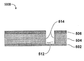
図4Dには、残るフォトレジスト層510と反射防止膜508が、酸素その他の混合気体による通常のプラズマまたはGCIBアッシング処理(例えば表2に示す処理条件で)され、得られる構造500Dが示されている。好ましい実施例として、多孔質ULK絶縁層504内のヴィア512の側壁を、GCIB処理(例えば表3に示す処理条件で)により清浄化、緻密化され、多孔質部分が表面に無い状態にすることができる。これによって、ウェットクリーン工程や、多孔質絶縁体のウェットプロセスによる汚染される機会を避けることができる。
In FIG. 4D, the remaining
図4Eには、ウエハに次のパターンを形成するために、反射防止膜516とフォトレジスト層518より成る別のマスキング材料層が堆積した構造500Eが示されている。マスキング材料層の反射防止膜の一部はエッチングされたヴィア(ヴィア512として示される)を充填し、表面を平坦にした上にフォトレジストが形成される。反射防止膜516およびフォトレジスト層518は共に前記同様の材料より成る。ヴィア充填層を除いて、反射防止膜516は(例えば)約200nmの厚みを有する。フォトレジスト層518は(例えば)約200nmの厚みを有する。この構造は従来技術の2Dに示す構造よりもシンプルで改善されており、フォトリワーク(photo rework)を実行すれば、GCIBアッシング処理によりフォトレジストおよび反射防止膜を除去することができる。
FIG. 4E shows a
図4Fには、所望のトレンチパターンをレジストに描いた後、RIEまたはGCIBエッチング処理によって、反射防止膜516、ハードマスク層506、多孔質なULK絶縁層504の一部を除去して形成されたトレンチ520が示されている。反射防止膜516の材料は、多孔質ULK絶縁層504の材料よりもエッチング速度が速く、ヴィア512の上側周辺部にエッチングされない突出部“フェンス(fences)”が残らないようになっている。(例えば表1に示される処理条件では、反射防止膜516と多孔質ULK絶縁層504のエッチング速度がNF3と、O2の混合ガスの組成により制御される)図4Gには、アッシング処理、好ましくはGCIBアッシング処理(例えば表3に示す処理条件)により、半製品500Gの表面から残っているフォトレジスト層518、反射防止膜516を除去した状態が示されている。さらにRIEまたはGCIBエッチング処理(例えば表1に示す処理条件)によりハードマスク層506を除去し、基板エッチングストップフィルム502を開口してヴィア512が完成するまでが示されている。
In FIG. 4F, after a desired trench pattern is drawn on a resist, the
図4Hには、最後のGCIB処理(例えば表3に示す処理条件)により全てのULK絶縁層の表面522が緻密化、平滑化されて完成した、第一の実施例である改良された二重ダマシン構造500Hが示されている。
FIG. 4H shows the improved double layer of the first embodiment, which is completed by densifying and smoothing the
図5A〜5Gには多孔質ULK絶縁体を用いて最終的に二重ダマシン集積構造600Gを形成した過程である本発明の第二の実施例が示されている。それは初めにトレンチパターンをハードマスクに形成したものである。
FIGS. 5A to 5G show a second embodiment of the present invention which is a process of finally forming a double damascene
図5Aには、第二の実施例として金属配線の上に絶縁フィルムを堆積した状態が示されている。この絶縁堆積層600Aはエッチングストップフィルム602、多孔質ULK絶縁層604、ハードマスク層606を有する。マスキング材料層は所望により反射防止膜608、フォトレジスト層610が前記絶縁堆積層上に形成され、図に示すような構造となっている。エッチングストップ材料は、従来公知の材料と同様であり、典型的には、Si3N4、SiCNである。エッチングストップフィルム602は厚み(例えば)約35nmである。多孔質ULK絶縁層604は厚み(例えば)約300nmである。ハードマスク層606はプロセス終了後において、二重ダマシン構造の一部として残留することはない。従って、従来の集積法とは異なり、ハードマスク層606として比較的高いk値を有するSiO2や、Si3N4を用いることができる。SiO2や、Si3N4は抗酸化性があり、フォトリワークが可能である。ハードマスク層606は厚み(例えば)約80nmである。この厚みは、ULKや基板エッチングストップに対するハードマスク材料のエッチング速度によって調製することができる。SiO2や、Si3N4に加えて他の好適なハードマスク材料として、SiCOH、SiC、SiCNなどが挙げられるが、これらに限定されるものではない。反射防止膜608は(例えば)約40nmの厚み、フォトレジスト層610は(例えば)約200nmの厚みを有する。反射防止膜608とフォトレジスト層610は、前記の他、公知の材料を用いることができる(限定されるものではない)。また、場合によっては、ハードマスク層506が形成される前に、ガスクラスターイオンビーム処理(表3に示す典型的な処理条件)により多孔質ULK絶縁層504の表面が緻密化およびシーリング処理することもできる。
FIG. 5A shows a state in which an insulating film is deposited on a metal wiring as a second embodiment. The insulating
図5Bには、フォトレジスト層610に所望のトレンチパターンを描き、RIEまたはGCIBエッチング処理(例えば表1に示す処理条件)により反射防止膜608、ハードマスク層606を通して、多孔質ULK絶縁層604までエッチングして、ハードマスク層606内にトレンチパターン612が形成された構造600Bを示している。
In FIG. 5B, a desired trench pattern is drawn on the
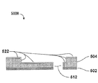
図5Cには、残っていたマスキング材料層が、酸素、窒素、水素、アルゴン、その他のガス(例えば表2に示す処理条件)を用いた通常のプラズマまたはGCIBアッシング処理によって除去され、同時に多孔質ULK絶縁層604の表面614が緻密化されている構造600Cを示している。
In FIG. 5C, the remaining masking material layer is removed by a normal plasma or GCIB ashing process using oxygen, nitrogen, hydrogen, argon, or other gases (for example, the processing conditions shown in Table 2) and at the same time porous. A structure 600C in which the
図5Dには、次のパターンをウエハに適用するために、別のマスキング材料層として反射防止膜616とフォトレジスト層618を含む層が形成された状態(構造600D)が示されている。反射防止膜616は(限定するものではないが)“AR40Anti−Reflectant”より成り、フォトレジスト層618は(これも限定するものではないが)“EpicTM2210ArF Photoresist”より成る。
FIG. 5D shows a state (
図5Eには、フォトレジスト層618に所望のヴィアパターンが描かれた後、RIEまたはGCIBエッチング処理によって、反射防止膜616、ハードマスク層606、多孔質ULK絶縁層604の一部を除去して、パターンを転写した状態が示されている。反射防止膜の材料はこの工程においてハードマスク層606と同程度のエッチング速度を有する。(例えば表1に示される処理条件では、反射防止膜616と多孔質ULK絶縁層604のエッチング速度がNF3と、O2の混合ガスの組成により制御される。)
In FIG. 5E, after a desired via pattern is drawn on the
図5Fには、通常のプラズマまたは、好ましくはGCIBアッシング処理(例えば表2の処理条件)により残存したマスキング材料を除去した半製品(構造600F)が示されている。
FIG. 5F shows a semi-finished product (
図5Gには、RIEまたはGCIBエッチング処理によりハードマスク層606を除去して、トレンチパターン612を多孔質ULK絶縁層604の中に形成してトレンチ624とし、同時にヴィアをエッチングして基板エッチングストップを開口しヴィア620を完成させた(例えば表1に示される処理条件)状態を示している。ハードマスク層606はこのプロセス中に完全に除去される。最後に、別のGCIB処理により、ULKの全表面622を平滑化、緻密化、シーリングを行う(例えば表2に示される処理条件)。GCIBエッチングは非常に指向性であり、従来のRIE処理では生じていたヴィアの側壁に、浅い斜面(従来技術の問題として示した図3G参照)が形成されることはない(実質的に斜面なし)。
In FIG. 5G, the
GCIB処理の重要な効果は、GCIB処理は、エッチングされたULK絶縁材料の平滑化、緻密化、シーリングができることにより、多孔質ULK絶縁材料を覆うハードマスクの必要性を失くした事である。ULK絶縁材料のハードマスクをRIEにより除去すると、多孔質ULK絶縁材料の表面が荒らされる。ULK絶縁材料のハードマスクをCMPにより除去すれば平滑化は可能であるが、緻密化、孔のシーリングができないために、多孔質ULK絶縁材料にウェット化学物質が侵入するという問題がある。 An important effect of the GCIB process is that the GCIB process can smooth, densify, and seal the etched ULK insulating material, thereby eliminating the need for a hard mask covering the porous ULK insulating material. When the hard mask of the ULK insulating material is removed by RIE, the surface of the porous ULK insulating material is roughened. Smoothing is possible if the hard mask of the ULK insulating material is removed by CMP, but there is a problem that wet chemical substances invade into the porous ULK insulating material because densification and hole sealing cannot be performed.
本発明の他の効果として、二重ダマシン構造の製造に際しハードマスクの使用数を最小にできること及び、最終のエッチングされた二重ダマシン構造からはハードマスクが除去されていることが挙げられる。従って、最終の二重ダマシン構造は十分に低いk値を有し、リークや層間剥離その他の関連する問題発生を最小にすることができるのである。多孔質なエッチングされたULK絶縁体の表面をすべて緻密化、シーリングすることで、後工程におけるCVDやALD処理中の汚染の影響を受け難くなる。最後に、GCIBエッチング処理は、マイクロローディング効果を受けることなく、トレンチの深さ、形状の制御が容易であり、共通の設計から抵抗とキャパシタンスのより正確な仕様が可能になる。 Other advantages of the present invention include the ability to minimize the number of hard masks used in the manufacture of the double damascene structure and the removal of the hard mask from the final etched double damascene structure. Thus, the final dual damascene structure has a sufficiently low k value to minimize the occurrence of leaks, delamination and other related problems. By densifying and sealing the entire surface of the porous etched ULK insulator, it becomes less susceptible to contamination during CVD or ALD processing in a later step. Finally, the GCIB etching process is easy to control the depth and shape of the trench without receiving the microloading effect, and allows more accurate specifications of resistance and capacitance from a common design.
以上、本発明を様々な具体例を示して説明したが、本発明の思想の範囲内でその他の改良・改善が可能であると理解されるべきである。 While the present invention has been described with reference to various specific examples, it should be understood that other improvements and improvements are possible within the scope of the idea of the present invention.
Claims (37)
基板エッチングストップフィルム層上に多孔質の極めて低いk値を有する絶縁フィルム層を形成する工程;
前記多孔質絶縁フィルム層上にハードマスク層を形成する工程;
前記ハードマスク層の上に第一のマスキング材料層を適用する工程;
前記第一のマスキング材料層の中にヴィアパターンを形成する工程;
側壁を露出するとともに1以上のヴィアを形成するために、前記ハードマスク層および前記多孔質絶縁フィルム層を通して第一のマスキング材料層内のヴィアパターンをエッチングストップフィルム層まで転写させる工程、;
ガスクラスターイオンビームの照射によって前記多孔質な絶縁フィルム層内の1以上のヴィアの側壁の上に緻密化層を形成する工程;
前記第一マスキング材料層の残部を除去する工程;
1以上の形成されたヴィアを充填し、前記ハードマスク層の上に層を形成するために第二のマスキング材料層を適用する工程;
前記第二のマスキング材料層内にトレンチパターンを形成する工程;
露出された表面と側壁に1以上のトレンチを形成するために、前記ハードマスク層および少なくとも一部の前記多孔質絶縁フィルム層を通して前記第二のマスキング材料層内のトレンチパターンを転写させる工程;
前記第二マスキング材料層の残部を除去する工程;
1以上のトレンチの表面および側壁上に緻密化層を形成する工程;
ハードマスク層の一部もしくは全部を除去して、1以上のヴィアを基板エッチングストップ層に開けるためにガスクラスターイオンビームの照射によってエッチングする工程
とを含むことを特徴とする、二重ダマシン集積構造を製造する方法。 A method of manufacturing a dual damascene integrated structure comprising:
Forming a porous insulating film layer having a very low k value on the substrate etching stop film layer;
Forming a hard mask layer on the porous insulating film layer;
Applying a first masking material layer over the hardmask layer;
Forming a via pattern in the first masking material layer;
Transferring the via pattern in the first masking material layer through the hard mask layer and the porous insulating film layer to an etch stop film layer to expose the sidewall and form one or more vias;
Forming a densified layer on one or more via sidewalls in the porous insulating film layer by irradiation with a gas cluster ion beam;
Removing the remainder of the first masking material layer;
Filling a one or more formed vias and applying a second masking material layer to form a layer over the hardmask layer;
Forming a trench pattern in the second masking material layer;
Transferring a trench pattern in the second masking material layer through the hard mask layer and at least a portion of the porous insulating film layer to form one or more trenches in exposed surfaces and sidewalls;
Removing the remainder of the second masking material layer;
Forming a densified layer on the surface and sidewalls of the one or more trenches;
A dual damascene integrated structure comprising: removing part or all of the hard mask layer and etching by irradiation with a gas cluster ion beam to open one or more vias in the substrate etching stop layer. How to manufacture.
基板エッチングストップフィルム層上に多孔質の極めて低いk値を有する絶縁フィルム層を形成する工程;
前記多孔質絶縁フィルム層上にハードマスク層を形成する工程;
前記ハードマスク層の上に第一のマスキング材料層を適用する工程;
前記第一のマスキング材料層の中にトレンチパターンを形成する工程;
多孔質絶縁フィルム層の表面を露出するとともに1以上のトレンチ開口を形成するために、前記ハードマスク層を通して、前記第一のマスキング材料層内のトレンチパターンを、少なくとも前記多孔質絶縁フィルム層内に転写させる工程;
ガスクラスターイオンビームの照射によって、前記多孔質絶縁フィルム層の1以上のトレンチ開口の露出された表面に、緻密化層を形成する工程;
前記第一マスキング材料層の残部を除去する工程;
1以上のトレンチ開口と、前記ハードマスク層の上に第二のマスキング材料層を適用する工程;
前記第二のマスキング材料層内にヴィアパターンを形成する工程;
1以上のヴィア開口を形成するために、少なくとも一部の前記多孔質絶縁フィルム層を通して、前記第二のマスキング材料層内のヴィアパターンを転写させる工程;
前記第二マスキング材料層の残部を除去する工程;
露出された側壁と表面を有する1以上のトレンチを完成するために1以上のトレンチ開口を深くし、露出された側壁を有する1以上のヴィアを完成するために1以上のヴィア開口を深くして、1以上のヴィア内に基板エッチングストップ層を開口することを含む、エッチング工程;
ハードマスク層を除去する工程;
露出された前記絶縁フィルム層の全ての表面および側壁上に、ガスクラスターイオンビーム照射により緻密化層を形成する工程;
とを含むことを特徴とする、二重ダマシン集積構造を製造する方法。 A method of manufacturing a dual damascene integrated structure comprising:
Forming a porous insulating film layer having a very low k value on the substrate etching stop film layer;
Forming a hard mask layer on the porous insulating film layer;
Applying a first masking material layer over the hardmask layer;
Forming a trench pattern in the first masking material layer;
To expose the surface of the porous insulating film layer and to form one or more trench openings, through the hard mask layer, a trench pattern in the first masking material layer is at least in the porous insulating film layer. A transferring step;
Forming a densified layer on the exposed surface of one or more trench openings of the porous insulating film layer by irradiation with a gas cluster ion beam;
Removing the remainder of the first masking material layer;
Applying a second masking material layer over the one or more trench openings and the hard mask layer;
Forming a via pattern in the second masking material layer;
Transferring a via pattern in the second masking material layer through at least a portion of the porous insulating film layer to form one or more via openings;
Removing the remainder of the second masking material layer;
One or more trench openings are deepened to complete one or more trenches having exposed sidewalls and surfaces, and one or more via openings are deepened to complete one or more vias having exposed sidewalls. An etching process comprising opening a substrate etch stop layer in one or more vias;
Removing the hard mask layer;
Forming a densified layer by gas cluster ion beam irradiation on all exposed surfaces and sidewalls of the insulating film layer;
A method of manufacturing a dual damascene integrated structure.
前記絶縁材料層が、実質的に緻密化され、実質的に孔が無い表面および側壁を有する、ことを特徴とする二重ダマシン構造。 The double damascene trench and via pattern includes a porous, very low k-value insulating material layer and a substrate etch stop material layer;
A double damascene structure wherein the insulating material layer has a substantially densified surface and sidewalls that are substantially free of holes.
ガスクラスターイオンビームを一部に照射することによって、多孔質で極めて低いk値を有する絶縁材料層の少なくとも一部をエッチングする工程;
とを含むことを特徴とする処理方法。 Forming a porous insulating material layer having a very low k value;
Etching at least a portion of the porous insulating material layer having a very low k value by irradiating a portion with a gas cluster ion beam;
The processing method characterized by including these.
Applications Claiming Priority (2)
| Application Number | Priority Date | Filing Date | Title |
|---|---|---|---|
| US57643904P | 2004-06-03 | 2004-06-03 | |
| PCT/US2005/019316 WO2005122224A2 (en) | 2004-06-03 | 2005-06-02 | Improved dual damascene integration structures and method of forming improved dual damascene integration structures |
Publications (2)
| Publication Number | Publication Date |
|---|---|
| JP2008502150A true JP2008502150A (en) | 2008-01-24 |
| JP2008502150A5 JP2008502150A5 (en) | 2008-09-11 |
Family
ID=35503817
Family Applications (1)
| Application Number | Title | Priority Date | Filing Date |
|---|---|---|---|
| JP2007515542A Withdrawn JP2008502150A (en) | 2004-06-03 | 2005-06-02 | Improved dual damascene integrated structure and method of manufacturing the same |
Country Status (4)
| Country | Link |
|---|---|
| US (3) | US20050272237A1 (en) |
| EP (1) | EP1759407A2 (en) |
| JP (1) | JP2008502150A (en) |
| WO (1) | WO2005122224A2 (en) |
Cited By (7)
| Publication number | Priority date | Publication date | Assignee | Title |
|---|---|---|---|---|
| JP2010003955A (en) * | 2008-06-23 | 2010-01-07 | Japan Aviation Electronics Industry Ltd | Processing device for solid surface |
| JP2010157379A (en) * | 2008-12-26 | 2010-07-15 | Japan Aviation Electronics Industry Ltd | Pore-sealing method of solid surface |
| WO2010147141A1 (en) * | 2009-06-16 | 2010-12-23 | 東京エレクトロン株式会社 | Film deposition method, pretreatment device, and treating system |
| JP2011171736A (en) * | 2010-02-17 | 2011-09-01 | Renesas Electronics Corp | Semiconductor device and method of manufacturing the same |
| JP2012204591A (en) * | 2011-03-25 | 2012-10-22 | Toshiba Corp | Film formation method and non-volatile storage device |
| JP2013055336A (en) * | 2011-09-01 | 2013-03-21 | Tel Epion Inc | Gas cluster ion beam etching process for achieving target etch process characteristics for composite materials |
| WO2015087689A1 (en) * | 2013-12-13 | 2015-06-18 | 富士フイルム株式会社 | Pattern formation method, and method for producing electronic device |
Families Citing this family (42)
| Publication number | Priority date | Publication date | Assignee | Title |
|---|---|---|---|---|
| US20040229452A1 (en) * | 2003-05-15 | 2004-11-18 | Johnston Steven W. | Densifying a relatively porous material |
| US7709344B2 (en) * | 2005-11-22 | 2010-05-04 | International Business Machines Corporation | Integrated circuit fabrication process using gas cluster ion beam etching |
| US20070218698A1 (en) * | 2006-03-16 | 2007-09-20 | Tokyo Electron Limited | Plasma etching method, plasma etching apparatus, and computer-readable storage medium |
| US7816253B2 (en) * | 2006-03-23 | 2010-10-19 | International Business Machines Corporation | Surface treatment of inter-layer dielectric |
| US7838428B2 (en) * | 2006-03-23 | 2010-11-23 | International Business Machines Corporation | Method of repairing process induced dielectric damage by the use of GCIB surface treatment using gas clusters of organic molecular species |
| US7781154B2 (en) * | 2006-03-28 | 2010-08-24 | Applied Materials, Inc. | Method of forming damascene structure |
| US8034722B2 (en) * | 2006-04-07 | 2011-10-11 | Taiwan Semiconductor Manufacturing Co., Ltd. | Method of forming dual damascene semiconductor device |
| US20080124924A1 (en) * | 2006-07-18 | 2008-05-29 | Applied Materials, Inc. | Scheme for copper filling in vias and trenches |
| US7618889B2 (en) * | 2006-07-18 | 2009-11-17 | Applied Materials, Inc. | Dual damascene fabrication with low k materials |
| US7884026B2 (en) * | 2006-07-20 | 2011-02-08 | United Microelectronics Corp. | Method of fabricating dual damascene structure |
| US7815815B2 (en) | 2006-08-01 | 2010-10-19 | Sony Corporation | Method and apparatus for processing the peripheral and edge portions of a wafer after performance of a surface treatment thereon |
| US7329956B1 (en) * | 2006-09-12 | 2008-02-12 | Taiwan Semiconductor Manufacturing Company, Ltd. | Dual damascene cleaning method |
| US20080090402A1 (en) * | 2006-09-29 | 2008-04-17 | Griselda Bonilla | Densifying surface of porous dielectric layer using gas cluster ion beam |
| US7622403B2 (en) * | 2006-12-19 | 2009-11-24 | Chartered Semiconductor Manufacturing Ltd. | Semiconductor processing system with ultra low-K dielectric |
| US8618663B2 (en) * | 2007-09-20 | 2013-12-31 | International Business Machines Corporation | Patternable dielectric film structure with improved lithography and method of fabricating same |
| US7709370B2 (en) | 2007-09-20 | 2010-05-04 | International Business Machines Corporation | Spin-on antireflective coating for integration of patternable dielectric materials and interconnect structures |
| US8084862B2 (en) | 2007-09-20 | 2011-12-27 | International Business Machines Corporation | Interconnect structures with patternable low-k dielectrics and method of fabricating same |
| JP2009094378A (en) * | 2007-10-11 | 2009-04-30 | Panasonic Corp | Semiconductor device and method for fabricating the same |
| US7981308B2 (en) * | 2007-12-31 | 2011-07-19 | Robert Bosch Gmbh | Method of etching a device using a hard mask and etch stop layer |
| US8202435B2 (en) * | 2008-08-01 | 2012-06-19 | Tel Epion Inc. | Method for selectively etching areas of a substrate using a gas cluster ion beam |
| US7947582B2 (en) * | 2009-02-27 | 2011-05-24 | Tel Epion Inc. | Material infusion in a trap layer structure using gas cluster ion beam processing |
| US8226835B2 (en) * | 2009-03-06 | 2012-07-24 | Tel Epion Inc. | Ultra-thin film formation using gas cluster ion beam processing |
| US8288271B2 (en) * | 2009-11-02 | 2012-10-16 | International Business Machines Corporation | Method for reworking antireflective coating over semiconductor substrate |
| US8334203B2 (en) * | 2010-06-11 | 2012-12-18 | International Business Machines Corporation | Interconnect structure and method of fabricating |
| US8835324B2 (en) * | 2011-07-01 | 2014-09-16 | United Microelectronics Corp. | Method for forming contact holes |
| US8513138B2 (en) | 2011-09-01 | 2013-08-20 | Tel Epion Inc. | Gas cluster ion beam etching process for Si-containing and Ge-containing materials |
| US8557710B2 (en) | 2011-09-01 | 2013-10-15 | Tel Epion Inc. | Gas cluster ion beam etching process for metal-containing materials |
| US8946081B2 (en) | 2012-04-17 | 2015-02-03 | International Business Machines Corporation | Method for cleaning semiconductor substrate |
| JP2013251358A (en) * | 2012-05-31 | 2013-12-12 | Toshiba Corp | Semiconductor device manufacturing method and semiconductor device |
| US8722542B2 (en) | 2012-06-08 | 2014-05-13 | Tel Epion Inc. | Gas cluster ion beam process for opening conformal layer in a high aspect ratio contact via |
| US8728947B2 (en) | 2012-06-08 | 2014-05-20 | Tel Epion Inc. | Gas cluster ion beam process for opening conformal layer in a high aspect ratio contact via |
| US9058983B2 (en) | 2013-06-17 | 2015-06-16 | International Business Machines Corporation | In-situ hardmask generation |
| US9209033B2 (en) | 2013-08-21 | 2015-12-08 | Tel Epion Inc. | GCIB etching method for adjusting fin height of finFET devices |
| US9330915B2 (en) * | 2013-12-10 | 2016-05-03 | Taiwan Semiconductor Manufacturing Co., Ltd. | Surface pre-treatment for hard mask fabrication |
| US9385086B2 (en) | 2013-12-10 | 2016-07-05 | Taiwan Semiconductor Manufacturing Co., Ltd. | Bi-layer hard mask for robust metallization profile |
| US9613906B2 (en) * | 2014-06-23 | 2017-04-04 | GlobalFoundries, Inc. | Integrated circuits including modified liners and methods for fabricating the same |
| US20160064239A1 (en) * | 2014-08-28 | 2016-03-03 | Taiwan Semiconductor Manufacturing Company, Ltd. | Method for Integrated Circuit Patterning |
| CN105789111B (en) * | 2014-12-18 | 2019-03-12 | 中芯国际集成电路制造(上海)有限公司 | The forming method of semiconductor structure |
| WO2016176569A1 (en) * | 2015-04-30 | 2016-11-03 | Tel Epion Inc. | Method of surface profile correction using gas cluster ion beam |
| US10535566B2 (en) | 2016-04-28 | 2020-01-14 | Taiwan Semiconductor Manufacturing Company, Ltd. | Semiconductor device and method of manufacture |
| US10522349B2 (en) | 2017-11-30 | 2019-12-31 | Taiwan Semiconductor Manufacturing Company, Ltd. | Anti-reflective coating by ion implantation for lithography patterning |
| US20230317468A1 (en) * | 2022-03-31 | 2023-10-05 | Nanya Technology Corporation | Reworking process for fabricating semiconductor device |
Family Cites Families (34)
| Publication number | Priority date | Publication date | Assignee | Title |
|---|---|---|---|---|
| US4423547A (en) | 1981-06-01 | 1984-01-03 | International Business Machines Corporation | Method for forming dense multilevel interconnection metallurgy for semiconductor devices |
| JP3169151B2 (en) * | 1992-10-26 | 2001-05-21 | 三菱電機株式会社 | Thin film forming equipment |
| JP3152018B2 (en) * | 1993-06-24 | 2001-04-03 | 双葉電子工業株式会社 | Method of manufacturing field emission device |
| US5814194A (en) * | 1994-10-20 | 1998-09-29 | Matsushita Electric Industrial Co., Ltd | Substrate surface treatment method |
| US5731624A (en) | 1996-06-28 | 1998-03-24 | International Business Machines Corporation | Integrated pad and fuse structure for planar copper metallurgy |
| US5985762A (en) | 1997-05-19 | 1999-11-16 | International Business Machines Corporation | Method of forming a self-aligned copper diffusion barrier in vias |
| US6492732B2 (en) * | 1997-07-28 | 2002-12-10 | United Microelectronics Corp. | Interconnect structure with air gap compatible with unlanded vias |
| SG70654A1 (en) | 1997-09-30 | 2000-02-22 | Ibm | Copper stud structure with refractory metal liner |
| US6171951B1 (en) * | 1998-10-30 | 2001-01-09 | United Microelectronic Corp. | Dual damascene method comprising ion implanting to densify dielectric layer and forming a hard mask layer with a tapered opening |
| US6159842A (en) * | 1999-01-11 | 2000-12-12 | Taiwan Semiconductor Manufacturing Company | Method for fabricating a hybrid low-dielectric-constant intermetal dielectric (IMD) layer with improved reliability for multilevel interconnections |
| JP2003521812A (en) * | 1999-12-06 | 2003-07-15 | エピオン コーポレイション | Gas cluster ion beam smoother |
| US6331227B1 (en) * | 1999-12-14 | 2001-12-18 | Epion Corporation | Enhanced etching/smoothing of dielectric surfaces |
| US6426249B1 (en) | 2000-03-16 | 2002-07-30 | International Business Machines Corporation | Buried metal dual damascene plate capacitor |
| US6452251B1 (en) | 2000-03-31 | 2002-09-17 | International Business Machines Corporation | Damascene metal capacitor |
| US6503827B1 (en) | 2000-06-28 | 2003-01-07 | International Business Machines Corporation | Method of reducing planarization defects |
| US6426304B1 (en) * | 2000-06-30 | 2002-07-30 | Lam Research Corporation | Post etch photoresist strip with hydrogen for organosilicate glass low-κ etch applications |
| US6537606B2 (en) * | 2000-07-10 | 2003-03-25 | Epion Corporation | System and method for improving thin films by gas cluster ion beam processing |
| US6455411B1 (en) * | 2000-09-11 | 2002-09-24 | Texas Instruments Incorporated | Defect and etch rate control in trench etch for dual damascene patterning of low-k dielectrics |
| US6475929B1 (en) * | 2001-02-01 | 2002-11-05 | Advanced Micro Devices, Inc. | Method of manufacturing a semiconductor structure with treatment to sacrificial stop layer producing diffusion to an adjacent low-k dielectric layer lowering the constant |
| JP4623934B2 (en) * | 2001-05-09 | 2011-02-02 | エクソジェネシス コーポレーション | Method and system to improve the action of artificial joints applying gas cluster ion beam technology |
| US6426558B1 (en) | 2001-05-14 | 2002-07-30 | International Business Machines Corporation | Metallurgy for semiconductor devices |
| EP1442153A4 (en) * | 2001-10-11 | 2007-05-02 | Epion Corp | Gcib processing to improve interconnection vias and improved interconnection via |
| JP3881562B2 (en) * | 2002-02-22 | 2007-02-14 | 三井造船株式会社 | SiC monitor wafer manufacturing method |
| US6936551B2 (en) * | 2002-05-08 | 2005-08-30 | Applied Materials Inc. | Methods and apparatus for E-beam treatment used to fabricate integrated circuit devices |
| US6888251B2 (en) | 2002-07-01 | 2005-05-03 | International Business Machines Corporation | Metal spacer in single and dual damascene processing |
| US6846741B2 (en) | 2002-07-24 | 2005-01-25 | International Business Machines Corporation | Sacrificial metal spacer damascene process |
| JP2006507670A (en) | 2002-11-08 | 2006-03-02 | エピオン コーポレーション | GCIB processing of integrated circuit interconnect structures |
| WO2004053945A2 (en) | 2002-12-12 | 2004-06-24 | Epion Corporation | Re-crystallization of semiconductor surface film and doping of semiconductor by energetic cluster irradiation |
| JP3895281B2 (en) * | 2003-02-18 | 2007-03-22 | Tdk株式会社 | Pattern forming method, magnetoresistive effect element and magnetic head manufacturing method using the same, head suspension assembly and magnetic disk apparatus |
| US7238604B2 (en) * | 2003-04-24 | 2007-07-03 | Intel Corporation | Forming thin hard mask over air gap or porous dielectric |
| US7223705B2 (en) * | 2003-05-06 | 2007-05-29 | Intel Corporation | Ambient gas treatment of porous dielectric |
| US20040229452A1 (en) * | 2003-05-15 | 2004-11-18 | Johnston Steven W. | Densifying a relatively porous material |
| US7088003B2 (en) * | 2004-02-19 | 2006-08-08 | International Business Machines Corporation | Structures and methods for integration of ultralow-k dielectrics with improved reliability |
| US7244674B2 (en) * | 2004-04-27 | 2007-07-17 | Agency For Science Technology And Research | Process of forming a composite diffusion barrier in copper/organic low-k damascene technology |
-
2005
- 2005-06-02 JP JP2007515542A patent/JP2008502150A/en not_active Withdrawn
- 2005-06-02 EP EP05755487A patent/EP1759407A2/en not_active Withdrawn
- 2005-06-02 US US11/143,831 patent/US20050272237A1/en not_active Abandoned
- 2005-06-02 WO PCT/US2005/019316 patent/WO2005122224A2/en not_active Application Discontinuation
- 2005-06-02 US US11/143,421 patent/US7759251B2/en not_active Expired - Fee Related
-
2008
- 2008-10-06 US US12/246,352 patent/US20090130861A1/en not_active Abandoned
Cited By (11)
| Publication number | Priority date | Publication date | Assignee | Title |
|---|---|---|---|---|
| JP2010003955A (en) * | 2008-06-23 | 2010-01-07 | Japan Aviation Electronics Industry Ltd | Processing device for solid surface |
| JP2010157379A (en) * | 2008-12-26 | 2010-07-15 | Japan Aviation Electronics Industry Ltd | Pore-sealing method of solid surface |
| WO2010147141A1 (en) * | 2009-06-16 | 2010-12-23 | 東京エレクトロン株式会社 | Film deposition method, pretreatment device, and treating system |
| JP2011003569A (en) * | 2009-06-16 | 2011-01-06 | Tohoku Univ | Film deposition method, pretreatment device, and treating system |
| CN102460653A (en) * | 2009-06-16 | 2012-05-16 | 东京毅力科创株式会社 | Film deposition method, pretreatment device, and treating system |
| US8865590B2 (en) | 2009-06-16 | 2014-10-21 | Tokyo Electron Limited | Film forming method, pretreatment device, and processing system |
| JP2011171736A (en) * | 2010-02-17 | 2011-09-01 | Renesas Electronics Corp | Semiconductor device and method of manufacturing the same |
| JP2012204591A (en) * | 2011-03-25 | 2012-10-22 | Toshiba Corp | Film formation method and non-volatile storage device |
| JP2013055336A (en) * | 2011-09-01 | 2013-03-21 | Tel Epion Inc | Gas cluster ion beam etching process for achieving target etch process characteristics for composite materials |
| WO2015087689A1 (en) * | 2013-12-13 | 2015-06-18 | 富士フイルム株式会社 | Pattern formation method, and method for producing electronic device |
| JP2015132811A (en) * | 2013-12-13 | 2015-07-23 | 富士フイルム株式会社 | Pattern formation method, and method for producing electronic device |
Also Published As
| Publication number | Publication date |
|---|---|
| EP1759407A2 (en) | 2007-03-07 |
| WO2005122224A3 (en) | 2006-11-09 |
| US20050272265A1 (en) | 2005-12-08 |
| US20050272237A1 (en) | 2005-12-08 |
| US20090130861A1 (en) | 2009-05-21 |
| US7759251B2 (en) | 2010-07-20 |
| WO2005122224A2 (en) | 2005-12-22 |
Similar Documents
| Publication | Publication Date | Title |
|---|---|---|
| JP2008502150A (en) | Improved dual damascene integrated structure and method of manufacturing the same | |
| US6812147B2 (en) | GCIB processing to improve interconnection vias and improved interconnection via | |
| US7115511B2 (en) | GCIB processing of integrated circuit interconnect structures | |
| KR101019356B1 (en) | Methods and apparatus of creating airgap in dielectric layers for the reduction of rc delay | |
| KR101184529B1 (en) | Copper interconnect wiring and method of forming thereof | |
| US6015760A (en) | Method for enhancing oxide to nitride selectivity through the use of independent heat control | |
| US7563379B2 (en) | Dry etching method and photonic crystal device fabricated by use of the same | |
| US7799683B2 (en) | Copper interconnect wiring and method and apparatus for forming thereof | |
| US8992785B2 (en) | Method for modifying an etch rate of a material layer using energetic charged particles | |
| TWI476862B (en) | Method for forming trench isolation using a gas cluster ion beam growth process | |
| US20070184656A1 (en) | GCIB Cluster Tool Apparatus and Method of Operation | |
| CN1624881A (en) | Selective etching of carbon-doped low-k dielectrics | |
| JP5539883B2 (en) | Method for improving electrical leakage characteristics and suppressing electromigration in semiconductor devices | |
| WO2009045718A1 (en) | Method to improve a copper/dielectric interface in semiconductor devices | |
| EP0814501A2 (en) | Method for etching metal silicide with high selectivity to polysilicon | |
| WO2007092856A2 (en) | Copper interconnect wiring and method and apparatus for forming thereof | |
| CN112490127A (en) | Method for correcting etching rate of material layer by using charged particles | |
| Kojima et al. | Dual-frequency superimposed RF capacitive-coupled plasma etch process | |
| JP7503650B2 (en) | Systems and methods for tungsten-containing film removal | |
| JP5227734B2 (en) | Method and apparatus for low energy electron enhanced etching and cleaning of substrates | |
| JP4607328B2 (en) | Method and apparatus for low energy electron enhanced etching and cleaning of substrates |
Legal Events
| Date | Code | Title | Description |
|---|---|---|---|
| A621 | Written request for application examination |
Free format text: JAPANESE INTERMEDIATE CODE: A621 Effective date: 20080602 |
|
| A521 | Request for written amendment filed |
Free format text: JAPANESE INTERMEDIATE CODE: A523 Effective date: 20080716 |
|
| A761 | Written withdrawal of application |
Free format text: JAPANESE INTERMEDIATE CODE: A761 Effective date: 20101102 |