JP2008293979A - Light source module and backlight assembly, display device with these, and method for reducing thickness of backlight assembly - Google Patents
Light source module and backlight assembly, display device with these, and method for reducing thickness of backlight assembly Download PDFInfo
- Publication number
- JP2008293979A JP2008293979A JP2008136336A JP2008136336A JP2008293979A JP 2008293979 A JP2008293979 A JP 2008293979A JP 2008136336 A JP2008136336 A JP 2008136336A JP 2008136336 A JP2008136336 A JP 2008136336A JP 2008293979 A JP2008293979 A JP 2008293979A
- Authority
- JP
- Japan
- Prior art keywords
- power supply
- supply plate
- light emitting
- emitting chip
- light
- Prior art date
- Legal status (The legal status is an assumption and is not a legal conclusion. Google has not performed a legal analysis and makes no representation as to the accuracy of the status listed.)
- Pending
Links
Images


Classifications
-
- H—ELECTRICITY
- H01—ELECTRIC ELEMENTS
- H01L—SEMICONDUCTOR DEVICES NOT COVERED BY CLASS H10
- H01L33/00—Semiconductor devices with at least one potential-jump barrier or surface barrier specially adapted for light emission; Processes or apparatus specially adapted for the manufacture or treatment thereof or of parts thereof; Details thereof
- H01L33/48—Semiconductor devices with at least one potential-jump barrier or surface barrier specially adapted for light emission; Processes or apparatus specially adapted for the manufacture or treatment thereof or of parts thereof; Details thereof characterised by the semiconductor body packages
- H01L33/483—Containers
- H01L33/486—Containers adapted for surface mounting
-
- G—PHYSICS
- G02—OPTICS
- G02F—OPTICAL DEVICES OR ARRANGEMENTS FOR THE CONTROL OF LIGHT BY MODIFICATION OF THE OPTICAL PROPERTIES OF THE MEDIA OF THE ELEMENTS INVOLVED THEREIN; NON-LINEAR OPTICS; FREQUENCY-CHANGING OF LIGHT; OPTICAL LOGIC ELEMENTS; OPTICAL ANALOGUE/DIGITAL CONVERTERS
- G02F1/00—Devices or arrangements for the control of the intensity, colour, phase, polarisation or direction of light arriving from an independent light source, e.g. switching, gating or modulating; Non-linear optics
- G02F1/01—Devices or arrangements for the control of the intensity, colour, phase, polarisation or direction of light arriving from an independent light source, e.g. switching, gating or modulating; Non-linear optics for the control of the intensity, phase, polarisation or colour
- G02F1/13—Devices or arrangements for the control of the intensity, colour, phase, polarisation or direction of light arriving from an independent light source, e.g. switching, gating or modulating; Non-linear optics for the control of the intensity, phase, polarisation or colour based on liquid crystals, e.g. single liquid crystal display cells
- G02F1/133—Constructional arrangements; Operation of liquid crystal cells; Circuit arrangements
- G02F1/1333—Constructional arrangements; Manufacturing methods
- G02F1/1335—Structural association of cells with optical devices, e.g. polarisers or reflectors
-
- G—PHYSICS
- G02—OPTICS
- G02B—OPTICAL ELEMENTS, SYSTEMS OR APPARATUS
- G02B6/00—Light guides; Structural details of arrangements comprising light guides and other optical elements, e.g. couplings
- G02B6/0001—Light guides; Structural details of arrangements comprising light guides and other optical elements, e.g. couplings specially adapted for lighting devices or systems
- G02B6/0011—Light guides; Structural details of arrangements comprising light guides and other optical elements, e.g. couplings specially adapted for lighting devices or systems the light guides being planar or of plate-like form
- G02B6/0081—Mechanical or electrical aspects of the light guide and light source in the lighting device peculiar to the adaptation to planar light guides, e.g. concerning packaging
- G02B6/0083—Details of electrical connections of light sources to drivers, circuit boards, or the like
-
- G—PHYSICS
- G02—OPTICS
- G02B—OPTICAL ELEMENTS, SYSTEMS OR APPARATUS
- G02B6/00—Light guides; Structural details of arrangements comprising light guides and other optical elements, e.g. couplings
- G02B6/0001—Light guides; Structural details of arrangements comprising light guides and other optical elements, e.g. couplings specially adapted for lighting devices or systems
- G02B6/0011—Light guides; Structural details of arrangements comprising light guides and other optical elements, e.g. couplings specially adapted for lighting devices or systems the light guides being planar or of plate-like form
- G02B6/0081—Mechanical or electrical aspects of the light guide and light source in the lighting device peculiar to the adaptation to planar light guides, e.g. concerning packaging
- G02B6/0086—Positioning aspects
- G02B6/009—Positioning aspects of the light source in the package
-
- G—PHYSICS
- G02—OPTICS
- G02F—OPTICAL DEVICES OR ARRANGEMENTS FOR THE CONTROL OF LIGHT BY MODIFICATION OF THE OPTICAL PROPERTIES OF THE MEDIA OF THE ELEMENTS INVOLVED THEREIN; NON-LINEAR OPTICS; FREQUENCY-CHANGING OF LIGHT; OPTICAL LOGIC ELEMENTS; OPTICAL ANALOGUE/DIGITAL CONVERTERS
- G02F1/00—Devices or arrangements for the control of the intensity, colour, phase, polarisation or direction of light arriving from an independent light source, e.g. switching, gating or modulating; Non-linear optics
- G02F1/01—Devices or arrangements for the control of the intensity, colour, phase, polarisation or direction of light arriving from an independent light source, e.g. switching, gating or modulating; Non-linear optics for the control of the intensity, phase, polarisation or colour
- G02F1/13—Devices or arrangements for the control of the intensity, colour, phase, polarisation or direction of light arriving from an independent light source, e.g. switching, gating or modulating; Non-linear optics for the control of the intensity, phase, polarisation or colour based on liquid crystals, e.g. single liquid crystal display cells
- G02F1/133—Constructional arrangements; Operation of liquid crystal cells; Circuit arrangements
- G02F1/1333—Constructional arrangements; Manufacturing methods
- G02F1/1335—Structural association of cells with optical devices, e.g. polarisers or reflectors
- G02F1/1336—Illuminating devices
- G02F1/133615—Edge-illuminating devices, i.e. illuminating from the side
-
- H—ELECTRICITY
- H01—ELECTRIC ELEMENTS
- H01L—SEMICONDUCTOR DEVICES NOT COVERED BY CLASS H10
- H01L2224/00—Indexing scheme for arrangements for connecting or disconnecting semiconductor or solid-state bodies and methods related thereto as covered by H01L24/00
- H01L2224/01—Means for bonding being attached to, or being formed on, the surface to be connected, e.g. chip-to-package, die-attach, "first-level" interconnects; Manufacturing methods related thereto
- H01L2224/42—Wire connectors; Manufacturing methods related thereto
- H01L2224/47—Structure, shape, material or disposition of the wire connectors after the connecting process
- H01L2224/48—Structure, shape, material or disposition of the wire connectors after the connecting process of an individual wire connector
- H01L2224/4805—Shape
- H01L2224/4809—Loop shape
- H01L2224/48095—Kinked
-
- H—ELECTRICITY
- H01—ELECTRIC ELEMENTS
- H01L—SEMICONDUCTOR DEVICES NOT COVERED BY CLASS H10
- H01L33/00—Semiconductor devices with at least one potential-jump barrier or surface barrier specially adapted for light emission; Processes or apparatus specially adapted for the manufacture or treatment thereof or of parts thereof; Details thereof
- H01L33/48—Semiconductor devices with at least one potential-jump barrier or surface barrier specially adapted for light emission; Processes or apparatus specially adapted for the manufacture or treatment thereof or of parts thereof; Details thereof characterised by the semiconductor body packages
- H01L33/52—Encapsulations
- H01L33/56—Materials, e.g. epoxy or silicone resin
-
- H—ELECTRICITY
- H01—ELECTRIC ELEMENTS
- H01L—SEMICONDUCTOR DEVICES NOT COVERED BY CLASS H10
- H01L33/00—Semiconductor devices with at least one potential-jump barrier or surface barrier specially adapted for light emission; Processes or apparatus specially adapted for the manufacture or treatment thereof or of parts thereof; Details thereof
- H01L33/48—Semiconductor devices with at least one potential-jump barrier or surface barrier specially adapted for light emission; Processes or apparatus specially adapted for the manufacture or treatment thereof or of parts thereof; Details thereof characterised by the semiconductor body packages
- H01L33/58—Optical field-shaping elements
- H01L33/60—Reflective elements
-
- H—ELECTRICITY
- H01—ELECTRIC ELEMENTS
- H01L—SEMICONDUCTOR DEVICES NOT COVERED BY CLASS H10
- H01L33/00—Semiconductor devices with at least one potential-jump barrier or surface barrier specially adapted for light emission; Processes or apparatus specially adapted for the manufacture or treatment thereof or of parts thereof; Details thereof
- H01L33/48—Semiconductor devices with at least one potential-jump barrier or surface barrier specially adapted for light emission; Processes or apparatus specially adapted for the manufacture or treatment thereof or of parts thereof; Details thereof characterised by the semiconductor body packages
- H01L33/62—Arrangements for conducting electric current to or from the semiconductor body, e.g. lead-frames, wire-bonds or solder balls
Abstract
Description
本発明は、光源モジュールとバックライトアセンブリ及びこれらを有する表示装置に関し、より詳細には、導光板の厚さを減少して表示装置をスリム化することのできる光源モジュールとバックライトアセンブリ及びこれらを有する表示装置並びにバックライトアセンブリの厚さを減少させる方法に関する。 The present invention relates to a light source module, a backlight assembly, and a display device having the same, and more specifically, a light source module, a backlight assembly, and a light source module that can reduce the thickness of a light guide plate and slim the display device. And a method of reducing the thickness of a backlight assembly.
一般的に液晶表示装置は、厚さが薄くて重さが軽く、電力消費が低いという長所があり、モニター、ノートブック、携帯電話のみならず、大型TVにも用いられる。液晶表示装置は、液晶の光透過率を用いて画像を表示する液晶表示パネル及び液晶表示パネルの下部に配置され、液晶表示パネルに光を提供するバックライトアセンブリを含む。 In general, a liquid crystal display device has the advantages of being thin, light in weight, and low in power consumption, and is used not only for monitors, notebooks and mobile phones, but also for large TVs. The liquid crystal display device includes a liquid crystal display panel that displays an image using light transmittance of the liquid crystal, and a backlight assembly that is disposed under the liquid crystal display panel and provides light to the liquid crystal display panel.
特に中小型液晶表示装置に用いられるバックライトアセンブリは、一般的に、光を発生する発光チップを有する光源モジュール及び側面が光源モジュールと向い合うように配置された導光板を含む。ここで、導光板の側面が光源モジュールと向い合うように配置されることによって、導光板は一般的に光源モジュールと対応する厚さを有する。 In particular, a backlight assembly used in a small-to-medium-sized liquid crystal display device generally includes a light source module having a light emitting chip that generates light and a light guide plate that is disposed so that a side surface faces the light source module. Here, the light guide plate generally has a thickness corresponding to that of the light source module by being disposed so that the side surface of the light guide plate faces the light source module.
しかしながら、このように、導光板が光源モジュールと対応する厚さを有することによって、バックライトアセンブリの合計厚さが増加し、それによって液晶表示装置の合計厚さが増加するという問題点がある。 However, since the light guide plate has a thickness corresponding to that of the light source module, the total thickness of the backlight assembly is increased, thereby increasing the total thickness of the liquid crystal display device.
そこで、本発明は上記従来の液晶表示装置における問題点に鑑みてなされたものであって、本発明の目的は、導光板の厚さを減少して表示装置をスリム化することのできる光源モジュールを提供することにある。
本発明の他の目的は、上記光源モジュールを具備するバックライトアセンブリを提供することにある。
本発明の更に他の目的は、上記バックライトアセンブリを具備する表示装置を提供することにある。
本発明の更に他の目的は、バックライトアセンブリの厚さを減少させる方法を提供することにある。
Accordingly, the present invention has been made in view of the above-mentioned problems in the conventional liquid crystal display device, and an object of the present invention is to reduce the thickness of the light guide plate and slim the display device. Is to provide.
Another object of the present invention is to provide a backlight assembly including the light source module.
Still another object of the present invention is to provide a display device having the above backlight assembly.
Still another object of the present invention is to provide a method for reducing the thickness of a backlight assembly.
上記目的を達成するためになされた本発明による光源モジュールは、電源供給板と、前記電源供給板の第1方向の中心から一側に片寄るように前記電源供給板上に配置され、前記電源供給板と電気的に接続される発光チップと、前記発光チップが露出するように前記電源供給板と結合される本体モールドとを有することを特徴とする。 The light source module according to the present invention, which has been made to achieve the above object, is disposed on the power supply plate so as to be offset from the center in the first direction of the power supply plate and the power supply plate. A light emitting chip electrically connected to the plate, and a main body mold coupled to the power supply plate so that the light emitting chip is exposed.
前記電源供給板は、前記第1方向と直交する第2方向に長く延長された形状を有することが好ましい。
前記電源供給板は、前記発光チップに第1電圧を供給する第1電圧供給板と、前記第1電圧供給板から前記第2方向に離隔し、前記発光チップに前記第1電圧と異なる第2電圧を供給する第2電圧供給板とを含むことが好ましい。
前記第1電圧供給板は、前記発光チップと電気的に接続される第1メイン本体部と、前記第1メイン本体部と結合され、外部の装置から前記第1電圧の供給を受ける第1サブ本体部とを含み、前記第2電圧供給板は、前記第1メイン本体部から前記第2方向に離隔し、前記発光チップと電気的に接続される第2メイン本体部と、前記第2メイン本体部と結合され、外部の装置から前記第2電圧の供給を受ける第2サブ本体部とを含むことが好ましい。
It is preferable that the power supply plate has a shape extending long in a second direction orthogonal to the first direction.
The power supply plate is separated from the first voltage supply plate in the second direction by supplying a first voltage supply plate for supplying a first voltage to the light emitting chip, and a second voltage different from the first voltage in the light emitting chip. It is preferable to include a second voltage supply plate that supplies a voltage.
The first voltage supply plate is coupled to the first main body part electrically connected to the light emitting chip, and the first sub body is coupled to the first main body part and receives the first voltage from an external device. A second main body part that is spaced apart from the first main body part in the second direction and is electrically connected to the light emitting chip; and a second main body part. It is preferable to include a second sub main body unit coupled to the main body unit and receiving the supply of the second voltage from an external device.
前記第1及び第2メイン本体部それぞれの前記第1方向の幅は、0.25〜0.4mmの範囲を有し、前記発光チップの前記第1方向の幅は、0.075mm〜0.125mmの範囲を有することが好ましい。
前記第1及び第2メイン本体部の前記第2方向の合計長さは、3〜4mmの範囲を有することが好ましい。
前記電源供給板の一側は、前記電源供給板の第1長辺であり、前記発光チップは電源供給板の他側である第2長辺より前記電源供給板の第1長辺に近接して配置されることが好ましい。
前記電源供給板に電気的に接続され、前記発光チップが過電圧を受けることを防止するツェナー(Zener)ダイオードを更に有することが好ましい。
Each of the first and second main main body portions has a width in the first direction of 0.25 to 0.4 mm, and the light emitting chip has a width in the first direction of 0.075 mm to 0.00 mm. Preferably it has a range of 125 mm.
The total length of the first and second main body portions in the second direction is preferably in the range of 3 to 4 mm.
One side of the power supply plate is a first long side of the power supply plate, and the light emitting chip is closer to the first long side of the power supply plate than a second long side which is the other side of the power supply plate. Are preferably arranged.
It is preferable to further include a Zener diode that is electrically connected to the power supply plate and prevents the light emitting chip from receiving an overvoltage.
一方、前記光源モジュールは、前記本体モールドの開口部を満たして前記発光チップを覆う蛍光物質を更に含むことができる。ここで、前記発光チップは、青色光を発光する青色発光ダイオードであるとき、前記蛍光物質は、前記青色光を白色光に変更するイエローフォスパー(yellow phosphor)を含むことが望ましい。 Meanwhile, the light source module may further include a fluorescent material that fills the opening of the body mold and covers the light emitting chip. Here, when the light emitting chip is a blue light emitting diode that emits blue light, the fluorescent material may include a yellow phosphor that changes the blue light into white light.
上記目的を達成するためになされた本発明によるバックライトアセンブリは、電源供給板と、前記電源供給板の第1方向の中心から一側に片寄るように前記電源供給板上に配置され前記電源供給板と電気的に接続される発光チップと、前記発光チップが露出するように前記電源供給板と結合する本体モールドとを含む光源モジュールと、前記発光チップと向い合うように配置され前記発光チップから発生した光を入射する側面と該側面から入射した光を出射する光出射面とを含む導光板とを有することを特徴とする。 The backlight assembly according to the present invention made to achieve the above object includes a power supply plate and the power supply plate disposed on the power supply plate so as to be shifted to one side from the center in the first direction of the power supply plate. A light source chip including a light emitting chip electrically connected to the plate, a main body mold coupled to the power supply plate so as to expose the light emitting chip, and a light source module disposed to face the light emitting chip. And a light guide plate including a side surface on which the generated light is incident and a light emitting surface on which the light incident from the side surface is emitted.
前記電源供給板は、前記第1方向と直交する第2方向に長く延長された形状を有することが好ましい。
前記導光板の厚さは、前記発光チップの前記第1方向の幅と同一であるか、或いは大きいことが好ましい。
前記導光板の厚さは、前記本体モールドに形成される開口部の前記第1方向の幅と同一であるか、或いは大きいことが好ましい。
It is preferable that the power supply plate has a shape extending long in a second direction orthogonal to the first direction.
The thickness of the light guide plate is preferably equal to or larger than the width of the light emitting chip in the first direction.
The thickness of the light guide plate is preferably equal to or larger than the width of the opening formed in the main body mold in the first direction.
前記導光板の一面に配置され、前記一面から出射される光の特性を向上させる少なくとも一枚の光学シートを更に有し、前記少なくとも一枚の光学シートと前記導光板の合計厚さは、前記光源モジュールの第1方向の幅と同一であるか、或いは小さいことが好ましい。 The light guide plate further includes at least one optical sheet disposed on one surface of the light guide plate to improve the characteristics of light emitted from the one surface, and the total thickness of the at least one optical sheet and the light guide plate is The width of the light source module is preferably equal to or smaller than the width in the first direction.
前記光源モジュールと電気的に接続され、前記光源モジュールに電源を供給する可撓性回路基板を更に有することが好ましい。
前記可撓性回路基板は、前記電源供給板の一側に片寄るように配置された前記発光チップと対向する電源供給板の他側に前記本体モールドと向い合うように配置されることが好ましい。
It is preferable to further include a flexible circuit board that is electrically connected to the light source module and supplies power to the light source module.
Preferably, the flexible circuit board is disposed on the other side of the power supply plate facing the light emitting chip so as to be offset toward one side of the power supply plate so as to face the main body mold.
上記目的を達成するためになされた本発明による表示装置は、光を用いて画像を表示する表示パネルと、電源供給板と、前記電源供給板の第1方向の中心から一側に片寄るように前記電源供給板上に配置され前記電源供給板と電気的に接続される発光チップと、前記発光チップが露出するように前記電源供給板と結合する本体モールドとを含む光源モジュールと、前記発光チップと向い合うように配置され前記発光チップから発生した光を入射する側面と該側面から入射した光を出射する光出射面とを含む導光板とを含むバックライトアセンブリとを有することを特徴とする。 In order to achieve the above object, a display device according to the present invention includes a display panel that displays an image using light, a power supply plate, and a power supply plate that is offset from the center in the first direction to one side. A light source module including a light emitting chip disposed on the power supply plate and electrically connected to the power supply plate, and a main body mold coupled to the power supply plate so that the light emitting chip is exposed, and the light emitting chip And a backlight assembly including a light guide plate including a side surface on which light generated from the light emitting chip is incident and a light emitting surface that emits light incident from the side surface. .
前記バックライトアセンブリは、前記光源モジュールと電気的に接続され前記光源モジュールに電源を供給する可撓性回路基板を更に含み、前記可撓性回路基板は、前記一側に片寄るように配置された前記発光チップと対向する他側に前記本体モールドと向い合うように配置されることが好ましい。
前記可撓性回路基板は、前記表示パネルの下面に少なくとも一部分が付着されて固定されることが好ましい。
前記導光板の厚さは、前記本体ホールドに形成される開口部の前記第1方向の幅と同一であるか、或いは大きいことが好ましい。
前記バックライトアセンブリは、前記導光板上に配置され、前記導光板から出射される光の特性を向上させる少なくとも一枚の光学シートを更に含み、前記少なくとも一枚の光学シートと前記導光板の合計厚さは、前記光源モジュールの第1方向の幅と同一であるか、或いは小さいことが好ましい。
The backlight assembly further includes a flexible circuit board that is electrically connected to the light source module and supplies power to the light source module, and the flexible circuit board is disposed to be offset toward the one side. It is preferable that the other side facing the light emitting chip is disposed so as to face the main body mold.
It is preferable that at least a part of the flexible circuit board is fixed to the lower surface of the display panel.
The thickness of the light guide plate is preferably equal to or larger than the width of the opening formed in the main body hold in the first direction.
The backlight assembly further includes at least one optical sheet disposed on the light guide plate and improving characteristics of light emitted from the light guide plate, and the total of the at least one optical sheet and the light guide plate. The thickness is preferably equal to or smaller than the width of the light source module in the first direction.
上記目的を達成するためになされた本発明によるバックライトアセンブリの厚さを減少させる方法は、第1方向の幅と第2方向の長さを有し、前記第2方向に延長された第1長辺及び第2長辺を備える電源供給板を提供する段階と、前記第1方向の幅と前記第2方向の長さを有する発光チップを前記第2長辺より前記第1長辺に近接して前記電源供給板上に配置する段階と、本体モールドで前記電源供給板を囲み、前記本体モールドに形成されて前記第1方向の幅を有する開口部を通じて前記発光チップを露出する段階と、前記本体モールドの開口部と隣接するように前記開口部の幅より小さい厚さを有する導光板を配置する段階とを有することを特徴とする。 In order to achieve the above object, a method for reducing the thickness of a backlight assembly according to the present invention has a width in a first direction and a length in a second direction, the first extending in the second direction. Providing a power supply plate having a long side and a second long side, and a light emitting chip having a width in the first direction and a length in the second direction closer to the first long side than the second long side And placing on the power supply plate, surrounding the power supply plate with a body mold, and exposing the light emitting chip through an opening formed in the body mold and having a width in the first direction, Disposing a light guide plate having a thickness smaller than the width of the opening so as to be adjacent to the opening of the main body mold.
本発明に係る光源モジュールとバックライトアセンブリ及びこれらを有する表示装置並びにバックライトアセンブリの厚さを減少させる方法よれば、発光チップが電源供給板の中心から第1方向の一側に片寄るように配置されることによって、発光チップで発生した光をガイドする導光板の厚さが減少して表示装置の厚さを更に減少させることができるという効果がある。
また、可撓性回路基板が表示パネルの下面に付着されて固定されることによって、可撓性回路基板上に配置された光源モールドが外部からの衝撃などによって動いてしまうことを防止することができるという効果がある。
According to the light source module, the backlight assembly, the display device having the light source module, and the method of reducing the thickness of the backlight assembly according to the present invention, the light emitting chip is disposed so as to be shifted to one side in the first direction from the center of the power supply plate. By doing so, there is an effect that the thickness of the light guide plate for guiding the light generated in the light emitting chip can be reduced and the thickness of the display device can be further reduced.
In addition, by attaching and fixing the flexible circuit board to the lower surface of the display panel, it is possible to prevent the light source mold disposed on the flexible circuit board from moving due to an external impact or the like. There is an effect that can be done.
次に、本発明に係る光源モジュールとバックライトアセンブリ及びこれらを有する表示装置並びにバックライトアセンブリの厚さを減少させる方法を実施するための最良の形態の具体例を図面を参照しながら説明する。
図1は、本発明の第1の実施形態による表示装置の一部を示す断面図である。
Next, a specific example of the best mode for carrying out the light source module, the backlight assembly, the display device having these, and the method for reducing the thickness of the backlight assembly according to the present invention will be described with reference to the drawings.
FIG. 1 is a cross-sectional view showing a part of a display device according to a first embodiment of the present invention.
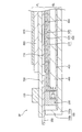
図1を参照すると、本実施形態による表示装置(DP)は、光を発生するバックライトアセンブリ(BL)及びバックライトアセンブリ(BL)で発生した光を用いて画像を表示する表示パネル(PL)を含む。 Referring to FIG. 1, the display device (DP) according to the present embodiment includes a backlight assembly (BL) that generates light and a display panel (PL) that displays an image using light generated by the backlight assembly (BL). including.
バックライトアセンブリ(BL)は、収納容器100、光源モジュール200、可撓性回路基板300、導光板400、反射シート450、光学部材500、及び接着シート600を含む。
The backlight assembly (BL) includes a
収納容器100は、底面部100a及び底面部のエッジから延長された少なくとも一つの側壁100bを含み、底面部100a及び側壁100bによって収納空間を形成する。
収納容器100は、収納空間に光源モジュール200、可撓性回路基板300、導光板400、反射シート450、光学部材500、接着シート600などを収納する。
The
The
光源モジュール200は、収納容器100内に収納され、具体的には、収納容器100の一側壁100bと隣接して配置される。光源モジュール200は、収納容器100の底部と平行方向に収納容器100の中心に向って光を出射する。ここで、光源モジュール200についての詳細な説明は別途の図面を参照して後述する。
The
可撓性回路基板300は、光源モジュール200と電気的に接続され、光源モジュール200に電源を供給する。即ち、光源モジュール200は、可撓性回路基板300上に配置され、可撓性回路基板300と電気的に接続され、可撓性回路基板300から電源の供給を受ける。ここで、可撓性回路基板300についてのより詳細な位置関係は、表示パネル(PL)について説明した後で説明する。
The
導光板400は、上面、上面と対向する下面、及び上面と下面とを連結する側面で構成する。導光板400は、側面が光源モジュール200と向い合うように収納容器100内に配置される。
導光板400は、光源モジュール200で発生した光を側面から入射し、入射した光をガイドして上面に出射する。また、導光板400の下面には複数の反射ドット(図示せず)を形成してもよい。
The
The
反射シート450は、導光板400と収納容器100の底面部100aとの間に配置される。反射シート450は、導光板400の下面から出射される光を反射して導光板400内に再入射させる。反射シート450は、光源モジュール200の下部を覆うように収納容器100の側面に沿って延長させることもできる。
The
光学部材500は、導光板400の上面上に配置され、上面から出射される光の光学特性を向上させる。即ち、光学部材500は、上面から出射される光の光学特性を向上させることができる少なくとも一枚の光学シートを含む。
The
一例として、光学部材500は、光を拡散して輝度均一性を向上させる拡散シート510、及び光の正面輝度を増加させる第1及び第2プリズムシート(520、530)を含む。具体的には、例えば、拡散シート510の厚さは、約58μmであってもよく、第1及び第2プリズムシート(520、530)の各厚さは約65μmであってもよい。よって、光学部材500の合計厚さは約0.188mmであってもよい。
As an example, the
接着シート600は、光学部材500と表示パネル(PL)との間に配置される。接着シート600は、一例として、光が透過するように中央が開口された四角形のフレーム形状を有することが望ましく、これとは違って、光の透過可能な透明な材質で形成することもできる。
The
接着シート600は、光学部材500のエッジ及び収納容器100の側面に付着され、光学シート500を収納容器100に固定することができる。このように、接着シート600が光学部材500を収納容器100に固定する場合、収納容器100内に収納されたその他の構成要素も収納容器100に固定することができる。また、接着シート600は、光学部材500を表示パネル(PL)の下面に付着することができる。それによって、バックライトアセンブリ(BL)を表示パネル(PL)の下面に付着することができる。
The
表示パネル(PL)は、第1基板700、第1基板700と対向する第2基板800、及び第1及び第2基板(700、800)の間に介在する液晶層(図示せず)を含む。
The display panel (PL) includes a
第1基板700は、画像駆動信号が伝送される信号線、信号線と電気的に接続された薄膜トランジスタ、及び薄膜トランジスタと電気的に接続され、透明な導電性物質からなる画素電極を含む。ここで、第1基板700の下面には第1偏光軸を有する第1偏光板710を配置することができ、第1基板700の上面には画像駆動信号を信号線に印加するための駆動チップ720が配置される。
The
第2基板800は、画素電極と対応するカラーフィルタ及び基板の全面に形成され、透明な導電性物質からなる共通電極を含む。ここで、カラーフィルタは、一例として、赤色カラーフィルタ、緑色カラーフィルタ、及び青色カラーフィルタを含む。あるいは、カラーフィルは、第2基板800ではない第1基板700に含んでもよい。ここで、第2基板800の上面には第1偏光軸と直交する第2偏光軸を有する第2偏光板810を配置することができる。
The
液晶層は、第1及び第2基板(700、800)の間に介在し、画素電極と共通電極との間に形成された電場によって液晶分子の配列が変更される。液晶層は、電場によって液晶分子の配列を変更させることによって、液晶層を透過する光の透過率を変更させる。 The liquid crystal layer is interposed between the first and second substrates (700 and 800), and the arrangement of liquid crystal molecules is changed by an electric field formed between the pixel electrode and the common electrode. The liquid crystal layer changes the transmittance of light transmitted through the liquid crystal layer by changing the arrangement of liquid crystal molecules by an electric field.
次に、可撓性回路基板300の位置関係を説明すると、可撓性回路基板300は、表示パネル(PL)の下面に付着されて固定される。具体的には、可撓性回路基板300の上面は、第1基板700の下面のエッジに付着させることができる。反面、可撓性回路基板300の下面には光源モジュール200が配置される。ここで、可撓性回路基板300の下面は、図1とは違って、少なくとも一部分が接着シート600のエッジに付着してもよい。
Next, the positional relationship of the
このように、可撓性回路基板300が表示パネル(PL)の下面に付着されて固定されることによって、可撓性回路基板300上に配置された光源モジュール200が外部からの衝撃などによって動いてしまうことを防止することができる。
As described above, the
図2は、図1の光源モジュールを示した斜視図であり、図3は、図2の光源モジュールから本体モールドを除いた状態を示した斜視図であり、図4は、図2のI−I’線に沿って見た断面図である。 2 is a perspective view showing the light source module of FIG. 1, FIG. 3 is a perspective view showing a state in which the main body mold is removed from the light source module of FIG. 2, and FIG. It is sectional drawing seen along I 'line.
図1、図2、図3、及び図4を参照すると、光源モジュール200は、電源供給板210、電源供給板210上に配置された発光チップ220、及び電源供給板210と結合される本体モールド230を含む。
Referring to FIGS. 1, 2, 3, and 4, the
電源供給板210は、第1方向に所定の幅を有し、第1方向と直交する第2方向に所定の長さを有することができる。即ち、電源供給板210は、第1方向より第2方向に長く延長された形状を有することができる。
The
具体的には、電源供給板210は、発光チップ220に第1電圧を印加する第1電圧供給板212及び発光チップ220に第1電圧と異なる第2電圧を印加する第2電圧供給板214を含む。
Specifically, the
第1電圧供給板212は、発光チップ220と直接電気的に接続される第1メイン本体部212a及び第1メイン本体部212aと接続されて外部から第1電圧の印加を受ける第1サブ本体部212bを含む。
The first
また、第2電圧供給板214は、第1メイン本体部212aから第2方向に離隔して発光チップ220と直接電気的に接続される第2メイン本体部214a及び第2メイン本体部214aと連結されて外部から第2電圧の印加を受ける第2サブ本体部214bを含む。
In addition, the second
第1及び第2メイン本体部(212a、214a)は、第1方向より第2方向に長い形状を有することが望ましい。ここで、第1メイン本体部212aの第1方向の幅は、第2メイン本体部214aの第1方向の幅と互いに同一であることが望ましい。
The first and second main body portions (212a, 214a) preferably have a shape that is longer in the second direction than in the first direction. Here, the width of the first
第1及び第2メイン本体部(212a、214a)それぞれの第1方向の幅は製造上の限界で最小0.25mm以上を有しなければならない。一例として、第1及び第2メイン本体部(212a、214a)それぞれの幅は、0.25mm〜0.4mmの範囲を有することができる。 The width in the first direction of each of the first and second main body portions (212a, 214a) must have a minimum of 0.25 mm or more due to manufacturing limitations. As an example, the width of each of the first and second main body parts (212a, 214a) may have a range of 0.25 mm to 0.4 mm.
一方、第1メイン本体部212aの第2方向の長さは、第2メイン本体部214aの第2方向の長さと同一であってもよいが、互いに異なってもよい。一例として、第1及び第2メイン本体部(212a、214a)の第2方向の合計長さは3mm〜4mmの範囲を有することができ、望ましくは約3.8mmを有する。
On the other hand, the length of the first
一方、第1メイン本体部212aと第2メイン本体部214aとの間に形成された離隔空間(SS)は、第1方向に沿って形成してもよいが、図3のように第1方向に傾いた方向に形成してもよい。
Meanwhile, the separation space (SS) formed between the first
第1サブ本体部212bは、第1メイン本体部212aの一端と接続され、第2サブ本体部214bは、第1サブ本体部212bと対向する第2メイン本体部214aの一端と接続される。例えば、第1サブ本体部212bは、第1メイン本体部212aに対して垂直になるように第1メイン本体部212aの一端と接続され、第2サブ本体部214bは、第2メイン本体部214aに対して垂直になるように第2メイン本体部214aの一端と接続される。
The
第1サブ本体部212bは、可撓性回路基板300と電気的に接続され、可撓性回路基板300から第1電圧の供給を受ける。第2サブ本体部214bは、可撓性回路基板300と電気的に接続されて可撓性回路基板300から第2電圧の供給を受ける。
The
発光チップ220は、第1及び第2メイン本体部(212a、214a)のうち、少なくとも一方の本体部上に配置される。即ち、発光チップ220は、図3のように、離隔空間(SS)をオーバーラップして第1及び第2メイン本体部(212a、214a)上に架けて配置してもよいが、第1及び第2メイン本体部(212a、214a)のうち、一方の本体部上にのみ配置してもよい。
The
発光チップ220は、第1方向より第2方向に長い形状を有することが望ましい。ここで、発光チップ220の第1方向の幅は一例として、0.075mm〜0.125mmの範囲を有することができる。
The
発光チップ220は、第1メイン本体部212aまたは第2メイン本体部214aの幅である第1方向の中心から一側である第1長辺に片寄るように配置される。具体的には、例えば、発光チップ220は、第1メイン本体部212aまたは第2メイン本体部214aの第1及び第2サブ本体部(212a、212b)が接続された辺と対向する第1長辺に近接するように配置される。
The
一方、第1メイン本体部212aの第1方向の他側である第2長辺には、第1サブ本体部212bが連結されることが望ましく、第2メイン本体部214aの第1方向のの他側である第2長辺には、第2サブ本体部214bが連結されることが望ましい。
On the other hand, the
発光チップ220は、一対の接続ワイヤ222によって第1及び第2メイン本体部(212a、214a)それぞれと電気的に接続することができる。その結果、発光チップ220は、第1メイン本体部212aから第1電圧の印加を受け、第2メイン本体部214aから第2電圧の印加を受ける。ここで、発光チップ220は、接続ワイヤ222によってではなく他の接続手段によって第1及び第2メイン本体部(212a、214a)それぞれと電気的に接続することもできる。
The
発光チップ220は、青色、緑色、及び赤色発光ダイオードのうち、少なくとも一つを含むことができる。具体的には、例えば、一つの光源モジュール200に白色光を発生するために青色、緑色、及び赤色発光ダイオードすべてを含むことができる。
これとは違って、一つの光源モジュール200が青色発光ダイオードを含み、他の光源モジュール200が緑色発光ダイオードを含み、更に他の光源モジュール200が赤色発光ダイオードを含むことができる。あるいは、発光チップ220は白色光を発生させるために白色発光ダイオードを含むこともできる。
The
In contrast, one
本体モールド230は、発光チップ220が露出されるように第1及び第2メイン本体部(212a、214a)の少なくとも一部を囲む。即ち、本体モールド230には発光チップ220を露出させるための開口部232が形成される。ここで、発光チップ220から発生した光は、開口部232を通じて導光板400の側面に入射される。
The
本体モールド230は、例えば、金型にモールディング液を注入してモールド成型物を形成するインジェクションモールド(injection mold)方式によって形成することができる。
本体モールド230がインジェクションモールド方式によって形成された後、第1及び第2サブ本体部(212b、214b)を本体モールド230の外郭に沿って折り曲げる。結果として、第1及び第2サブ本体部(212b、214b)は、一例として、「L」字形状を有して折り曲げることができる。
The
After the
図5は、図2のII−II’線に沿って見た断面図である。
図1、図2、及び図5を参照すると、導光板400の側面と向い合う本体モールド230の一面は、図1における配置から見て開口部232を境として上側面234及び下側面236に区分される。即ち、上側面234は本体モールド230の一面のうち、開口部232の上側に形成された部分を示し、下側面236は本体モールド230の一面のうち、開口部232の下側に形成された部分を示す。ここで、下側面236は図5とは違って形成しなくてもよい。
FIG. 5 is a cross-sectional view taken along the line II-II ′ of FIG.
Referring to FIGS. 1, 2, and 5, one surface of the
開口部232の第1方向の幅(W1)は、発光チップ220の第1方向の幅と同一であるか大きいことが望ましい。発光チップ220が電源供給部210の第1方向の中心から一側に片寄って配置されるので、上側面234の第1方向の幅(W2)は、下側面236の第1方向の幅(W3)より大きくなる。従って、本体モールドの第1方向の幅(TW)は第1及び第2メイン本体部(212a、214a)それぞれの第1方向の幅と同一であるか大きいことが望ましい。
The width (W1) of the
具体的には、例えば、開口部232の第1方向の幅(W1)は約0.1mmであり、上側面234の第1方向の幅(W2)は約0.27mmであり、下側面236の第1方向の幅(W3)は、0.03mmであってもよい。従って、本体モールドの第1方向の幅(TW)は、0.4mmであってもよい。
Specifically, for example, the width (W1) in the first direction of the
導光板400の厚さ及び光学部材500の厚さを光源モジュール200の厚さと比較を下記に示す。
導光板400の厚さは発光チップ220の第1方向の幅と対応することができる。即ち、導光板400の厚さは発光チップ220の第1方向の幅と同一であるか、あるいは若干大きいことが望ましい。
A comparison of the thickness of the
The thickness of the
または、導光板400の厚さは、本体モールド230の開口部232の第1方向の幅(W1)と対応することができる。即ち、導光板400の厚さは、開口部232の第1方向の幅(W1)と同一であるか若干大きいことが望ましい。
Alternatively, the thickness of the
あるいはまた、導光板400の厚さは、開口部232の第1方向の幅(W1)と下側面236の第1方向の幅(W3)との和と対応することができる。即ち、導光板400の厚さは、開口部232の第1方向の幅(W1)と下側面236の第1方向の幅(W3)との和と同一であるか、あるいは若干大きいことが望ましい。
Alternatively, the thickness of the
一方、導光板400と光学部材500の合計厚さは、光源モジュール200、即ち、本体モールド230の第1方向の幅(TW)と同一であるか、或いは小さいことが望ましい。ここで、光学部材500の厚さは上側面234の第1方向の幅(W2)と同一であるか、小さいことが望ましい。
Meanwhile, the total thickness of the
図6は、図4とは異なる本発明の第2の実施形態を示した断面図である。
図2、図4、及び図6を参照すると、光源モジュール200は、本体モールド230の開口部232を満たして発光チップ220を覆う蛍光物質240を更に含むことができる。ここで、蛍光物質240は、発光チップ220で発生した光を白色光に変更させることが望ましい。
FIG. 6 is a cross-sectional view showing a second embodiment of the present invention different from FIG.
Referring to FIGS. 2, 4, and 6, the
具体的には例えば、発光チップ220は、青色光を発光させる青色発光ダイオードであり、蛍光物質240は青色光を白色光に変更させる黄色蛍光体(yellow phosphor)を含むことができる。
Specifically, for example, the
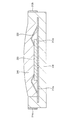
図7は、図3とは異なる本発明の第3の実施形態を示した斜視図である。
図2、図3、及び図7を参照すると、光源モジュール200は、電源供給板210と電気的に接続され、発光チップ220に過電圧が加わることを防止するツェナーダイオード250を更に含むことができる。
FIG. 7 is a perspective view showing a third embodiment of the present invention different from FIG.
Referring to FIGS. 2, 3, and 7, the
具体的に説明すると、ツェナーダイオード250は、発光チップ220と並列になるように第1及び第2メイン本体部(212a、214a)とそれぞれ電気的に接続することができる。即ち、ツェナーダイオード250は、一対の接続ワイヤ252によって第1及び第2メイン本体部(212a、214a)とそれぞれ電気的に接続することができる。ここで、発光チップ220が第1及び第2メイン本体部(212a、214a)のいずれの本体部上に配置されるとき、ツェナーダイオード250は、第1及び第2メイン本体部(212a、214a)の残りの本体部上に配置されることが望ましい。
Specifically, the
上述したように、これら本発明の実施形態によれば、発光チップ220が電源供給板210の第1方向の中心から一側に片寄るように配置されることによって、発光チップ220から発生した光をガイドする導光板400の厚さをより減少させることができる。
As described above, according to the embodiments of the present invention, the
また、光学部材500の側面が本体モールド230の上側面234と向い合うように配置され、光学部材500の厚さが上側面234の第1方向の幅(W2)と同一であるか、或いは小さい大きさを有することによって、バックライトアセンブリ(BL)の厚さをより減少させることができる。
Further, the side surface of the
また、可撓性回路基板300が表示パネル100の下面に付着されて固定されることによって、可撓性回路基板300上に配置された光源モジュール200が外部からの衝撃などによって動いてしまうことを防止することができる。
In addition, since the
尚、本発明は、上述の実施形態に限られるものではない。本発明の技術的範囲から逸脱しない範囲内で多様に変更実施することが可能である。 The present invention is not limited to the embodiment described above. Various modifications can be made without departing from the technical scope of the present invention.
100 収納容器
100a 底面部
100b 側壁
200 光源モジュール
210 電源供給板
212 第1電圧供給板
212a 第1メイン本体部
212b 第1サブ本体部
214 第2電圧供給板
214a 第2メイン本体部
214b 第2サブ本体部
220 発光チップ
222、252 接続ワイヤ
230 本体モールド
232 開口部
234 上側面
236 下側面
240 蛍光物質
250 ツェナーダイオード
300 可撓性回路基板
400 導光板
450 反射シート
500 光学部材
510 拡散シート
520、530 (第1及び第2)プリズムシート
600 接着シート
700 第1基板
710 第1偏光板
720 駆動チップ
800 第2基板
810 第2偏光板
DESCRIPTION OF
Claims (21)
前記電源供給板の第1方向の中心から一側に片寄るように前記電源供給板上に配置され、前記電源供給板と電気的に接続される発光チップと、
前記発光チップが露出するように前記電源供給板と結合される本体モールドとを有することを特徴とする光源モジュール。 A power supply plate;
A light emitting chip disposed on the power supply plate so as to be offset from the center in the first direction of the power supply plate, and electrically connected to the power supply plate;
A light source module comprising: a main body mold coupled to the power supply plate so that the light emitting chip is exposed.
前記第1電圧供給板から前記第2方向に離隔し、前記発光チップに前記第1電圧と異なる第2電圧を供給する第2電圧供給板とを含むことを特徴とする請求項2に記載の光源モジュール。 The power supply plate includes a first voltage supply plate that supplies a first voltage to the light emitting chip;
The second voltage supply plate according to claim 2, further comprising a second voltage supply plate that is spaced apart from the first voltage supply plate in the second direction and supplies a second voltage different from the first voltage to the light emitting chip. Light source module.
前記第1メイン本体部と結合され、外部の装置から前記第1電圧の供給を受ける第1サブ本体部とを含み、
前記第2電圧供給板は、前記第1メイン本体部から前記第2方向に離隔し、前記発光チップと電気的に接続される第2メイン本体部と、
前記第2メイン本体部と結合され、外部の装置から前記第2電圧の供給を受ける第2サブ本体部とを含むことを特徴とする請求項3に記載の光源モジュール。 The first voltage supply plate includes a first main body portion electrically connected to the light emitting chip;
A first sub body unit coupled to the first main body unit and receiving the first voltage from an external device;
The second voltage supply plate is spaced apart from the first main body portion in the second direction and electrically connected to the light emitting chip;
4. The light source module according to claim 3, further comprising: a second sub body unit coupled to the second main body unit and receiving the second voltage from an external device.
前記発光チップの前記第1方向の幅は、0.075mm〜0.125mmの範囲を有することを特徴とする請求項4に記載の光源モジュール。 The width in the first direction of each of the first and second main body portions has a range of 0.25 to 0.4 mm,
The light source module according to claim 4, wherein a width of the light emitting chip in the first direction has a range of 0.075 mm to 0.125 mm.
前記発光チップと向い合うように配置され前記発光チップから発生した光を入射する側面と該側面から入射した光を出射する光出射面とを含む導光板とを有することを特徴とするバックライトアセンブリ。 A power supply plate, a light emitting chip disposed on the power supply plate so as to be shifted to one side from the center in the first direction of the power supply plate, and the light emitting chip exposed. A light source module including a main body mold coupled to the power supply plate,
A backlight assembly, comprising: a light guide plate that is disposed to face the light emitting chip and includes a side surface on which light generated from the light emitting chip is incident; and a light emitting surface that emits light incident on the side surface. .
前記少なくとも一枚の光学シートと前記導光板の合計厚さは、前記光源モジュールの第1方向の幅と同一であるか、或いは小さいことを特徴とする請求項10に記載のバックライトアセンブリ。 It further includes at least one optical sheet disposed on one surface of the light guide plate and improving the characteristics of light emitted from the one surface,
The backlight assembly of claim 10, wherein a total thickness of the at least one optical sheet and the light guide plate is equal to or smaller than a width of the light source module in the first direction.
電源供給板と、前記電源供給板の第1方向の中心から一側に片寄るように前記電源供給板上に配置され前記電源供給板と電気的に接続される発光チップと、前記発光チップが露出するように前記電源供給板と結合する本体モールドとを含む光源モジュールと、
前記発光チップと向い合うように配置され前記発光チップから発生した光を入射する側面と該側面から入射した光を出射する光出射面とを含む導光板とを含むバックライトアセンブリとを有することを特徴とする表示装置。 A display panel for displaying an image using light;
A power supply plate, a light emitting chip disposed on the power supply plate so as to be shifted to one side from the center in the first direction of the power supply plate, and the light emitting chip exposed. A light source module including a main body mold coupled to the power supply plate,
A backlight assembly including a light guide plate that is disposed to face the light emitting chip and includes a side surface on which light generated from the light emitting chip is incident and a light emitting surface that emits light incident on the side surface. Characteristic display device.
前記可撓性回路基板は、前記一側に片寄るように配置された前記発光チップと対向する他側に前記本体モールドと向い合うように配置されることを特徴とする請求項16に記載の表示装置。 The backlight assembly further includes a flexible circuit board that is electrically connected to the light source module and supplies power to the light source module.
The display according to claim 16, wherein the flexible circuit board is disposed so as to face the main body mold on the other side facing the light emitting chip disposed so as to be offset toward the one side. apparatus.
前記少なくとも一枚の光学シートと前記導光板の合計厚さは、前記光源モジュールの第1方向の幅と同一であるか、或いは小さいことを特徴とする請求項16に記載の表示装置。 The backlight assembly further includes at least one optical sheet disposed on the light guide plate and improving characteristics of light emitted from the light guide plate,
The display device according to claim 16, wherein a total thickness of the at least one optical sheet and the light guide plate is equal to or smaller than a width in the first direction of the light source module.
前記第1方向の幅と前記第2方向の長さを有する発光チップを前記第2長辺より前記第1長辺に近接して前記電源供給板上に配置する段階と、
本体モールドで前記電源供給板を囲み、前記本体モールドに形成されて前記第1方向の幅を有する開口部を通じて前記発光チップを露出する段階と、
前記本体モールドの開口部と隣接するように前記開口部の幅より小さい厚さを有する導光板を配置する段階とを有することを特徴とするバックライトアセンブリの厚さを減少させる方法。
Providing a power supply plate having a width in a first direction and a length in a second direction and having a first long side and a second long side extended in the second direction;
Arranging a light emitting chip having a width in the first direction and a length in the second direction on the power supply plate closer to the first long side than the second long side;
Surrounding the power supply plate with a body mold, exposing the light emitting chip through an opening formed in the body mold and having a width in the first direction;
Disposing a light guide plate having a thickness smaller than the width of the opening adjacent to the opening of the main body mold, and reducing the thickness of the backlight assembly.
Applications Claiming Priority (1)
| Application Number | Priority Date | Filing Date | Title |
|---|---|---|---|
| KR1020070050619A KR101352921B1 (en) | 2007-05-25 | 2007-05-25 | Light source module, back-light assembly having the light source module and display apparatus having the back-light assembly |
Publications (2)
| Publication Number | Publication Date |
|---|---|
| JP2008293979A true JP2008293979A (en) | 2008-12-04 |
| JP2008293979A5 JP2008293979A5 (en) | 2011-07-07 |
Family
ID=39714129
Family Applications (1)
| Application Number | Title | Priority Date | Filing Date |
|---|---|---|---|
| JP2008136336A Pending JP2008293979A (en) | 2007-05-25 | 2008-05-26 | Light source module and backlight assembly, display device with these, and method for reducing thickness of backlight assembly |
Country Status (5)
| Country | Link |
|---|---|
| US (1) | US8053968B2 (en) |
| EP (1) | EP1995795A3 (en) |
| JP (1) | JP2008293979A (en) |
| KR (1) | KR101352921B1 (en) |
| CN (1) | CN101311616B (en) |
Cited By (1)
| Publication number | Priority date | Publication date | Assignee | Title |
|---|---|---|---|---|
| KR101295146B1 (en) | 2008-12-19 | 2013-08-09 | 엘지디스플레이 주식회사 | Liquid crystal display device |
Families Citing this family (12)
| Publication number | Priority date | Publication date | Assignee | Title |
|---|---|---|---|---|
| TWI368336B (en) * | 2007-07-12 | 2012-07-11 | Chi Mei Lighting Tech Corp | Light emitting diode device and applications thereof |
| JP5499905B2 (en) * | 2010-05-28 | 2014-05-21 | 三菱電機株式会社 | Display / lighting device |
| TWI531840B (en) * | 2011-05-24 | 2016-05-01 | 友達光電股份有限公司 | Backlight module |
| US20140232945A1 (en) * | 2011-09-30 | 2014-08-21 | Sharp Kabushiki Kaisha | Display device and television device |
| KR102023457B1 (en) * | 2011-12-21 | 2019-09-20 | 엘지이노텍 주식회사 | Reflector plate and backlight unit including the plate |
| JP5927056B2 (en) * | 2012-06-14 | 2016-05-25 | ルネサスエレクトロニクス株式会社 | Semiconductor device |
| KR102068766B1 (en) * | 2013-01-22 | 2020-01-21 | 엘지디스플레이 주식회사 | LED assembly and liquid crystal display device using the same |
| DE102014208960A1 (en) * | 2014-05-12 | 2015-11-12 | Osram Opto Semiconductors Gmbh | Surface-mountable optoelectronic component and method for producing a surface-mountable optoelectronic component |
| JP6323806B2 (en) * | 2014-06-30 | 2018-05-16 | パナソニックIpマネジメント株式会社 | Light emitting device and moving body |
| CN104360528B (en) * | 2014-11-18 | 2017-06-06 | 深圳市华星光电技术有限公司 | A kind of display module |
| US11019412B2 (en) | 2018-05-04 | 2021-05-25 | Red E Innovations, Llc | System for monitoring an injection mold or stamping die |
| CN110174801B (en) * | 2019-05-30 | 2024-03-26 | 武汉华星光电技术有限公司 | Display module |
Citations (1)
| Publication number | Priority date | Publication date | Assignee | Title |
|---|---|---|---|---|
| JP2001345485A (en) * | 2000-06-02 | 2001-12-14 | Toyoda Gosei Co Ltd | Light emitting device |
Family Cites Families (19)
| Publication number | Priority date | Publication date | Assignee | Title |
|---|---|---|---|---|
| JPH08201805A (en) | 1995-01-31 | 1996-08-09 | Minolta Co Ltd | Illumination structure of liquid crystal display surface |
| US6054716A (en) * | 1997-01-10 | 2000-04-25 | Rohm Co., Ltd. | Semiconductor light emitting device having a protecting device |
| KR100708511B1 (en) * | 2000-03-17 | 2007-04-16 | 마츠시타 덴끼 산교 가부시키가이샤 | Light-emitting semiconductor device and surface-emitting device |
| EP1204151A4 (en) | 2000-04-24 | 2006-10-18 | Rohm Co Ltd | Edge-emitting light-emitting semiconductor device and method of manufacture thereof |
| JP3930710B2 (en) * | 2000-09-13 | 2007-06-13 | シチズン電子株式会社 | Chip-type light emitting diode and manufacturing method thereof |
| JP4379786B2 (en) * | 2003-11-11 | 2009-12-09 | 株式会社エンプラス | Surface light source device |
| JP2005260276A (en) * | 2003-12-03 | 2005-09-22 | Sumitomo Electric Ind Ltd | Light-emitting device |
| JP2005191530A (en) | 2003-12-03 | 2005-07-14 | Sumitomo Electric Ind Ltd | Light emitting device |
| JP4070795B2 (en) | 2004-03-24 | 2008-04-02 | 株式会社ルネサス柳井セミコンダクタ | Method for manufacturing light emitting device |
| JP4902114B2 (en) * | 2004-12-16 | 2012-03-21 | 日亜化学工業株式会社 | Light emitting device |
| KR20060104795A (en) | 2005-03-31 | 2006-10-09 | 삼성에스디아이 주식회사 | Back light unit of flat panel display device |
| KR100665216B1 (en) * | 2005-07-04 | 2007-01-09 | 삼성전기주식회사 | Side-view light emitting diode having improved side-wall reflection structure |
| KR100638874B1 (en) | 2005-07-06 | 2006-10-27 | 삼성전기주식회사 | Light source-guide structure of backlight apparatus with led light source inserted into light guide plate and backlight apparatus having the same |
| JP4701904B2 (en) * | 2005-08-03 | 2011-06-15 | ソニー株式会社 | Electro-optical device and electronic apparatus |
| KR100736670B1 (en) | 2005-08-08 | 2007-07-06 | 희성전자 주식회사 | High-efficient LED Back Light Unit |
| JP4966199B2 (en) * | 2005-09-20 | 2012-07-04 | ルネサスエレクトロニクス株式会社 | LED light source |
| DE102006032416A1 (en) * | 2005-09-29 | 2007-04-05 | Osram Opto Semiconductors Gmbh | Radiation-emitting component |
| JP2009510230A (en) * | 2005-09-30 | 2009-03-12 | ザ リージェンツ オブ ザ ユニバーシティ オブ カリフォルニア | Nitrido and oxynitridocerium-based phosphor materials for solid-state lighting applications |
| TWI368336B (en) * | 2007-07-12 | 2012-07-11 | Chi Mei Lighting Tech Corp | Light emitting diode device and applications thereof |
-
2007
- 2007-05-25 KR KR1020070050619A patent/KR101352921B1/en active IP Right Grant
-
2008
- 2008-03-27 EP EP08005720A patent/EP1995795A3/en not_active Ceased
- 2008-04-28 US US12/110,486 patent/US8053968B2/en not_active Expired - Fee Related
- 2008-05-23 CN CN200810098330.3A patent/CN101311616B/en not_active Expired - Fee Related
- 2008-05-26 JP JP2008136336A patent/JP2008293979A/en active Pending
Patent Citations (1)
| Publication number | Priority date | Publication date | Assignee | Title |
|---|---|---|---|---|
| JP2001345485A (en) * | 2000-06-02 | 2001-12-14 | Toyoda Gosei Co Ltd | Light emitting device |
Cited By (1)
| Publication number | Priority date | Publication date | Assignee | Title |
|---|---|---|---|---|
| KR101295146B1 (en) | 2008-12-19 | 2013-08-09 | 엘지디스플레이 주식회사 | Liquid crystal display device |
Also Published As
| Publication number | Publication date |
|---|---|
| CN101311616A (en) | 2008-11-26 |
| CN101311616B (en) | 2014-04-23 |
| EP1995795A3 (en) | 2009-02-11 |
| KR20080103634A (en) | 2008-11-28 |
| KR101352921B1 (en) | 2014-01-24 |
| EP1995795A2 (en) | 2008-11-26 |
| US8053968B2 (en) | 2011-11-08 |
| US20080291365A1 (en) | 2008-11-27 |
Similar Documents
| Publication | Publication Date | Title |
|---|---|---|
| JP2008293979A (en) | Light source module and backlight assembly, display device with these, and method for reducing thickness of backlight assembly | |
| KR101620024B1 (en) | Display apparatus and method of assembling the same | |
| JP5367995B2 (en) | Backlight assembly, display module including the same, and manufacturing method thereof | |
| JP2008304887A (en) | Liquid crystal display | |
| US10488689B2 (en) | Display device | |
| US20160103267A1 (en) | Display apparatus | |
| CN106896554B (en) | Display device | |
| US7880825B2 (en) | Backlight assembly and liquid crystal display device having the same | |
| US8654274B2 (en) | Backlight assembly and liquid crystal display device including the same | |
| KR102268966B1 (en) | Display apparatus | |
| KR101834350B1 (en) | Display apparatus | |
| JP2008181135A (en) | Display apparatus and method for assembling the same | |
| KR20150051470A (en) | Back light assembly and display apparatus having the same | |
| KR20080070279A (en) | Back light assembly and display apparatus having the same | |
| KR102211702B1 (en) | Display panel and display apparatus having the same | |
| KR101920760B1 (en) | Liquid crystal display module inculding backlight unit | |
| JP2015068972A (en) | Liquid crystal display device | |
| KR102073649B1 (en) | Back light assembly and display apparatus having the same | |
| KR20130015792A (en) | Flexible printed circuit and liquid crystal display device | |
| KR102170086B1 (en) | Connector | |
| KR101740735B1 (en) | Liquid crystal display device | |
| KR102465447B1 (en) | LED FPCB Tape module and Display device having the same | |
| KR20070074889A (en) | Back light unit and liquid crystaldisplay device using the same | |
| KR20080075573A (en) | Liquid crystal display device | |
| KR20170080321A (en) | Display device |
Legal Events
| Date | Code | Title | Description |
|---|---|---|---|
| A521 | Request for written amendment filed |
Free format text: JAPANESE INTERMEDIATE CODE: A523 Effective date: 20110524 |
|
| A621 | Written request for application examination |
Free format text: JAPANESE INTERMEDIATE CODE: A621 Effective date: 20110524 |
|
| A521 | Request for written amendment filed |
Free format text: JAPANESE INTERMEDIATE CODE: A523 Effective date: 20120508 |
|
| A977 | Report on retrieval |
Free format text: JAPANESE INTERMEDIATE CODE: A971007 Effective date: 20121119 |
|
| A131 | Notification of reasons for refusal |
Free format text: JAPANESE INTERMEDIATE CODE: A131 Effective date: 20121127 |
|
| A711 | Notification of change in applicant |
Free format text: JAPANESE INTERMEDIATE CODE: A712 Effective date: 20121213 |
|
| A601 | Written request for extension of time |
Free format text: JAPANESE INTERMEDIATE CODE: A601 Effective date: 20130227 |
|
| A602 | Written permission of extension of time |
Free format text: JAPANESE INTERMEDIATE CODE: A602 Effective date: 20130304 |
|
| A521 | Request for written amendment filed |
Free format text: JAPANESE INTERMEDIATE CODE: A523 Effective date: 20130327 |
|
| A02 | Decision of refusal |
Free format text: JAPANESE INTERMEDIATE CODE: A02 Effective date: 20130611 |