JP2008290355A - Printing apparatus - Google Patents
Printing apparatus Download PDFInfo
- Publication number
- JP2008290355A JP2008290355A JP2007138663A JP2007138663A JP2008290355A JP 2008290355 A JP2008290355 A JP 2008290355A JP 2007138663 A JP2007138663 A JP 2007138663A JP 2007138663 A JP2007138663 A JP 2007138663A JP 2008290355 A JP2008290355 A JP 2008290355A
- Authority
- JP
- Japan
- Prior art keywords
- laser
- output
- laser output
- current
- monitor
- Prior art date
- Legal status (The legal status is an assumption and is not a legal conclusion. Google has not performed a legal analysis and makes no representation as to the accuracy of the status listed.)
- Pending
Links
Images


Abstract
Description
本発明は、レーザを感光体に照射することにより感光体上に潜像を作成する印刷装置において、印刷装置の制御部が予め設定された値でのレーザの特性を測定し、その測定されたレーザの特性を使ってレーザのパワーコントロールを行うことを特徴とする印刷装置に関する。 According to the present invention, in a printing apparatus that creates a latent image on a photosensitive member by irradiating the photosensitive member with a laser, the control unit of the printing apparatus measures a laser characteristic at a preset value, and the measurement is performed. The present invention relates to a printing apparatus that performs laser power control using characteristics of a laser.
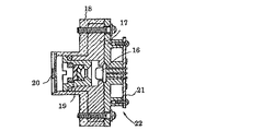
図5はレーザビームプリンタ等の電子写真装置に使われる半導体レーザユニットの構造を示す断面図である。この図において、16は半導体レーザ(レーザダイオード)、17はこの半導体レーザ16を支持しているベース金属板、18は電気的絶縁材、19は半導体レーザ16からの発散性光束を平行光束に変換するコリメータレンズ、20はビーム整形用のアパーチャ、21はプリンタ回路基板(PCB)を各々示し、これらは一体的なユニットとして組立てられて半導体レーザユニット22を構成している。
FIG. 5 is a sectional view showing the structure of a semiconductor laser unit used in an electrophotographic apparatus such as a laser beam printer. In this figure, 16 is a semiconductor laser (laser diode), 17 is a base metal plate supporting the
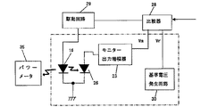
図6は、この半導体レーザユニット22をレーザプリンタ等の画像形成装置に装着してフイードバック制御ループを形成した状態のブロック図である。 FIG. 6 is a block diagram showing a state in which the semiconductor laser unit 22 is mounted on an image forming apparatus such as a laser printer to form a feedback control loop.
この図において、26は半導体レーザ16の発光出力をモニタするためのフォトダイオードで、そのモニタ電流をモニタ出力増幅器23に入力する。
In this figure,
比較器28と駆動回路29はレーザユニット以外の外部ボードに設けられており、比較器28はモニタ出力増幅器23の出力電圧Vmと基準電圧発生回路25が出力する内部基準電圧Vrとを比較し、両電圧が一致するように、半導体レーザ16に駆動電流を流して発光させる駆動回路29を制御する。
The
前記モニタ出力増幅器23は図7に示すように、オペアンプ31とその帰還回路を形成する利得調整用可変抵抗器32によって構成されている。
As shown in FIG. 7, the
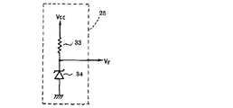
また、基準電圧発生回路25は図8に示すように、電源電圧Vccが供給される電源端子とアース間に直列に接続した抵抗33とツェナダイオード34とによって構成され、そのツェナダイオード34のツェナ電圧を内部基準電圧Vrとして出力する。
Further, as shown in FIG. 8, the reference
このように、半導体レーザユニット22に一体的に、利得調整可能な出力増幅器23及び基準電圧発生回路25を備えており、予め個々の半導体レーザユニット毎に、モニタ出力増幅器23の出力電圧Vmが、半導体レーザ16の出力パワーが感光体上で所期の値(標準設定パワー)となった時に、内部基準電圧Vrと一致するようにその利得を調整すると共に、基準電圧発生回路25を設定しておく。それによって、半導体レーザユニット交換の際に現場で調整をする必要がない。
As described above, the semiconductor laser unit 22 is integrally provided with the
この半導体レーザユニット22の製造段階では、個々の半導体レーザユニット22について次のような調整が行なわれる。図6において半導体レーザ16から出射したレーザ光の一部はモニタ用フォトダイオード26にも入射され、そのモニタ電流がモニタ出力増幅器23に入力される。
In the manufacturing stage of the semiconductor laser unit 22, the following adjustment is performed for each semiconductor laser unit 22. In FIG. 6, part of the laser light emitted from the
ここで、同じく半導体レーザ16から出射されたレーザ光を感光体上で受光するように配置したパワーメータ35で測定して、その測定値を確認しつつ、所定の標準設定パワーが得られるようにモニタ出力増幅器23の利得調整用可変抵抗32を調整する。その標準設定パワーが得られたときのモニタ出力増幅器23の出力電圧Vmに相当する電圧(同じ電圧)を内部基準電圧Vrとして発生するように基準電圧発生回路25を設定する。例えば、図8に示すツェナダイオード34のツェナ電圧を選択しておく。
Here, the laser beam emitted from the
このように、調整された半導体レーザユニット22を使用し、製品出荷後の保守作業でレーザユニット22を交換する場合でもパワーメータ35を用いることなく、レーザプリンタ本体側に設けられている図2の比較器28と駆動回路29にこの半導体レーザユニット22を接続することで、モニタ出力増幅器23の出力電圧Vmは基準電圧発生回路25から発生される基準電圧Vrと比較器28で比較され、これらの差を零にするように選択された電流が駆動回路29から半導体レーザ16に流されて、モニタ出力増幅器23の出力電圧Vmが内部基準電圧Vrと一致するように、半導体レーザ16の出力が制御され、標準設定パワーが得られる。
As described above, even when the adjusted semiconductor laser unit 22 is used and the laser unit 22 is replaced in maintenance work after product shipment, the
この種の技術に関しては、例えば下記のような特許文献を挙げることができる。 For example, the following patent documents can be cited regarding this type of technology.
背景技術に示すレーザ制御方法は、レーザ出力制御の基準値はレーザ出力を予めレーザ出力メータを使用して設定した固定値である。そのため実使用状況により、例えば印刷濃度を出荷時に調整した値より濃くしたい場合にレーザ強度を強くしたいとき、レーザ出力を合わせるためにレーザ光が当たる位置にレーザ出力メータを設置して調整を行うことが必要であり、製品出荷後の稼動状態にレーザ出力の変更を行うことは困難であった。 In the laser control method shown in the background art, the reference value for laser output control is a fixed value in which the laser output is set in advance using a laser output meter. Therefore, depending on the actual usage situation, for example, if you want to increase the laser intensity when you want to make the print density higher than the value adjusted at the time of shipment, install a laser output meter at the position where the laser light hits and adjust it to match the laser output Therefore, it is difficult to change the laser output to the operating state after product shipment.
例えば、レーザ出力制御の基準値となる基準電圧を複数搭載して切り替えることによってレーザ出力の切り替えは可能であるが、予め搭載している基準電圧値に対応した設定のみであり、用紙の種類や使用用途に対応するには不十分なものとなっていた。そのためオペレータがレーザ出力の変更は行うことができず、印刷濃度やコントラストの調整を行う場合は現像バイアスの電圧や感光体を感光させるチャージャ電圧を変えていた。現像バイアスの電圧やチャージャ電圧を変えた場合、印刷全体が薄くなってしまったりカブリが発生したりすることが多く、高品質の印刷は困難であった。 For example, it is possible to switch the laser output by mounting and switching a plurality of reference voltages as reference values for laser output control, but only the setting corresponding to the reference voltage value mounted in advance, the type of paper and It was insufficient for the purpose of use. For this reason, the operator cannot change the laser output, and when adjusting the print density and contrast, the voltage of the developing bias and the charger voltage for exposing the photosensitive member are changed. When the developing bias voltage and the charger voltage are changed, the whole printing often becomes thin or fog occurs, and high quality printing is difficult.
本発明の目的は、このような従来技術の欠点を解消し、優れた印刷品質を有する印刷装置を提供することにある。 An object of the present invention is to eliminate such drawbacks of the prior art and provide a printing apparatus having excellent print quality.
上記目的を達成するため本発明の第1の手段は、半導体レーザを感光体に照射することにより感光体上に潜像を作成する印刷装置において、前記半導体レーザのスロープ効率を考慮したパワーコントロールを行うことを特徴とするものである。 In order to achieve the above object, a first means of the present invention is a printing apparatus that creates a latent image on a photoconductor by irradiating the photoconductor with a semiconductor laser, and performs power control in consideration of the slope efficiency of the semiconductor laser. It is characterized by doing.
本発明の第2の手段は前記第1の手段において、前記パワーコントロールは、レーザ発光強度を検出するフォトダイオードまたはフォトトランジスタの特性、およびレーザダイオードとフォトダイオードまたはフォトトランジスタ間の伝達係数の個体差によってレーザ発光強度が同じでもフォトダイオードまたはフォトトランジスタのモニタ電流が異なってくることを補正してレーザ出力を制御することを特徴とするものである。 According to a second means of the present invention, in the first means, the power control includes a characteristic of a photodiode or a phototransistor for detecting a laser emission intensity, and an individual difference in a transfer coefficient between the laser diode and the photodiode or the phototransistor. The laser output is controlled by correcting that the monitor current of the photodiode or phototransistor differs even when the laser emission intensity is the same.
本発明のレーザ出力制御は、工場出荷時に調整されるレーザ出力とレーザ出力のモニタ電流の関係を記憶し、レーザユニットの特性を把握することによって希望するレーザ出力時に出力されるモニタ電流を算出し、算出されたモニタ電流を出力するレーザ出力で制御することにより任意のレーザ出力での制御を行い、印刷品質を向上することを可能とする。 The laser output control of the present invention stores the relationship between the laser output adjusted at the time of factory shipment and the monitor current of the laser output, and calculates the monitor current output at the desired laser output by grasping the characteristics of the laser unit. By controlling with the laser output that outputs the calculated monitor current, it is possible to control with an arbitrary laser output and improve the print quality.
本発明では、工場出荷時に調整されるレーザ出力とレーザ出力のモニタ電流によりレーザユニットの特性を把握し、希望するレーザ出力設定を連続的に切り替えることを可能として、希望するレーザ出力での制御が可能となる。 In the present invention, it is possible to grasp the characteristics of the laser unit from the laser output adjusted at the time of shipment from the factory and the monitor current of the laser output, and to continuously switch the desired laser output setting. It becomes possible.
前記レーザ出力とレーザ出力のモニタ電流の関係を記憶して、レーザユニットの特性を把握することによって希望するレーザ出力時に出力されるモニタ電流を算出し、算出されたモニタ電流を出力するレーザ出力で制御することを簡単な回路で実現した。 The relationship between the laser output and the monitor current of the laser output is stored, the monitor current output at the desired laser output is calculated by grasping the characteristics of the laser unit, and the calculated monitor current is output by the laser output. Control was realized with a simple circuit.
本発明における実施例を図1ないし図4を用いて説明する。図1は本発明におけるレーザ出力制御の概略フローチャート、図2はレーザ出力制御のブロック図、図3はレーザ電流とレーザ出力の特性図、図4はレーザ出力とモニタ電流の特性図である。 An embodiment of the present invention will be described with reference to FIGS. 1 is a schematic flowchart of laser output control in the present invention, FIG. 2 is a block diagram of laser output control, FIG. 3 is a characteristic diagram of laser current and laser output, and FIG. 4 is a characteristic diagram of laser output and monitor current.
本発明では、まずレーザユニットの特定のレーザ出力時のモニタ電流を制御部に記録しておく。図1ではこの特定のレーザ出力時のモニタ電流を使ったパワー調整方法を説明する。レーザユニットの起動時に特定のレーザ出力時のモニタ電流から伝達関数の算出を行う(Step1)。次に算出した伝達関数と実際に使用したいレーザ出力の値から実際に使用する条件でのモニタ電流の算出を行う(Step2)。次にモニタ電流の算出で算出したモニタ電流の値と実際のモニタ電流が一致するようにレーザ出力調整を行う(Step3)。 In the present invention, first, the monitor current at the time of a specific laser output of the laser unit is recorded in the control unit. FIG. 1 illustrates a power adjustment method using a monitor current at the time of outputting a specific laser. When the laser unit is activated, a transfer function is calculated from the monitor current at the time of specific laser output (Step 1). Next, the monitor current is calculated under the conditions of actual use from the calculated transfer function and the value of the laser output that is actually desired (Step 2). Next, laser output adjustment is performed so that the monitor current value calculated in the monitor current calculation matches the actual monitor current (Step 3).
モニタ電流がモニタ電流の算出の値と一致するということは、実際に使用したいレーザ出力になっているということである。またレーザビームを使用した印刷装置では印刷中にレーザ出力のパワー調整を定期的に行うが、実際に使用するレーザ出力の設定を変えない場合は、一度算出したモニタ電流を記録しておくことによりパワーの伝達関数の算出やモニタ電流の算出の処理は省略することができる。 The fact that the monitor current matches the value calculated for the monitor current means that the laser output is actually desired to be used. In printers that use laser beams, the laser output power is periodically adjusted during printing. If you do not want to change the actual laser output settings, record the monitor current once calculated. The process of calculating the power transfer function and the monitor current can be omitted.
図3は、レーザダイオード14の電流とレーザ出力との関係を示す特性図である。この図に示すようにレーザは閾値電流を超えると出力が上昇し、閾値以上ではレーザ電流とレーザ出力はほぼリニアな関係を示すが閾値電流および電流とレーザ出力の関係を示すスロープ効率はレーザの個体差があり一定ではない。
FIG. 3 is a characteristic diagram showing the relationship between the current of the
図4は、レーザ出力とモニタ電流との関係を示す特性図である。この図に示すように、レーザが30mWの出力時にはモニタ電流は最大で6mA、最小で4mAとなる。レーザの個体の特性によりこのレーザ出力とモニタ電流の関係も一定ではないが比例関係となる。 FIG. 4 is a characteristic diagram showing the relationship between laser output and monitor current. As shown in this figure, when the laser output is 30 mW, the monitor current is 6 mA at the maximum and 4 mA at the minimum. Depending on the characteristics of the individual laser, the relationship between the laser output and the monitor current is not constant but proportional.
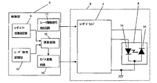
図2に示す本発明の代表的なブロック図を用いて本発明のレーザ出力の切り替えの説明を行う。本発明はレーザ出力任意設定値9とレーザ特性記憶部10とレーザ発光回路11と演算回路12とレーザ強度設定回路13からなる制御部5、およびレーザドライバ7とレーザ8からなるレーザユニット6で構成され、レーザ8はレーザダイオード14とレーザの発光強度をモニタするフォトダイオード15から構成される。図2ではレーザ8はレーザダイオード14とフォトダイオード15を有する形としているが、レーザダイオード14とフォトダイオード15は別体式でも本発明の実施は可能である。
The switching of laser output according to the present invention will be described with reference to a typical block diagram of the present invention shown in FIG. The present invention comprises a laser output arbitrary setting value 9, a laser
図3に示すように、レーザダイオード14は電流が一定の閾値電流に達するまで発光しないが、閾値電流を超えるとレーザ出力と電流はほぼ比例関係となり、このときの電流とレーザ出力の比がスロープ効率となる。但し、レーザダイオード14は個体差によって前記の閾値電流とスロープ効率が異なっているため、電流の値を一定としてもレーザダイオード14が異なるとレーザ出力が異なってくる。そのため電流でフイードバックを行ってもレーザダイオード14の出力を一定に保つことはできず、正確なレーザ出力の制御を行うためにフォトダイオード15でレーザ光を電流に変換する。フォトダイオード15はレーザ出力を電流に変換する。図4に示すようにフォトダイオード15はレーザ出力とモニタ電流は線形の関係にありレーザユニット6の固有の値となる。
As shown in FIG. 3, the
そのため図4で示す特性では、レーザ出力30mWの値はモニタ電流は最大6mA、最小4mAとなる。したがってレーザユニット6の個体ごとの特性(モニタ電流I/レーザ出力P)が個々のレーザユニット6の重要なパラメータとなる。
Therefore, in the characteristics shown in FIG. 4, the value of the laser output of 30 mW has a maximum monitor current of 6 mA and a minimum of 4 mA. Therefore, the characteristics of each laser unit 6 (monitor current I / laser output P) are important parameters of the
次に、制御部5の説明を行う。制御部5内のレーザ出力任意設定値9は実際に使用するオペレータなどが設定できる値であり、印刷装置のオペレータパネル(図示せず)より設定、もしくは印刷装置自身が温度や湿度などの環境条件を検出し設定する値である。レーザ特性記憶部10は前記のレーザユニット6のパラメータ(モニタ電流I/レーザ出力P)を記憶する部分でありNV−SRAM等の記憶素子が使用される。演算回路12はレーザ出力任意設定値9に設定された値とレーザ特性記憶部10の値を演算する部位であり、(モニタ電流I/レーザ出力P)×(レーザ出力任意設定値)からレーザダイオード14のレーザ出力任意設定値9でのフォトダイオード15のモニタ電流を算出する。算出はデジタルデータで行われるためD/A変換回路13でアナログ変換され、レーザ出力任意設定値9でレーザ14が発光した場合のフォトダイオード15のモニタ電流をレーザドライバ7に出力する。
Next, the control unit 5 will be described. The laser output arbitrary setting value 9 in the control unit 5 is a value that can be set by an operator or the like actually used, and is set from an operator panel (not shown) of the printing apparatus, or the printing apparatus itself has environmental conditions such as temperature and humidity. Is a value to detect and set The laser
レーザドライバ7は前述の算出されたフォトダイオード15のモニタ電流と実際のフォトダイオード15の出力が一致するように、レーザダイオード14を駆動するレーザドライバである。レーザダイオード14のレーザ出力はD/A変換回路13によって決定されるが、レーザのON/OFFはレーザ駆動信号発生回路11からの信号で行う。
The laser driver 7 is a laser driver that drives the
本発明では、レーザ7の特性を制御部5が持っているため希望するパワーをレーザ出力任意設定値9に設定するだけで、レーザ出力メータ等の器具を使わず調整が可能である。また、D/A変換回路13の分解能力で決まる分解能でレーザ出力を切り替えることができる。たとえばD/A変換回路13が10ビットのD/A変換器であれば1024段階のレーザ出力調整が可能である。
In the present invention, since the control unit 5 has the characteristics of the laser 7, the desired power can be set to the laser output arbitrary setting value 9 and adjustment can be performed without using a tool such as a laser output meter. Further, the laser output can be switched with a resolution determined by the resolution capability of the D /
したがって印刷装置が写真などのイメージを印刷する場合などの階調性を良くしたい場合はレーザ出力を弱く調整し、バーコードなど明瞭なコントラストが必要な場合はレーザ出力を強くするといった微細な調整が可能となる。レーザ出力任意設定値9をオペレータパネルにインジケータのバーもしくはパーセント表示の数字で表示することを行えばオペレータ自身が使用する目的に合わせて設定することが可能であり多目的な印刷で高品質な印刷を実現できる。 Therefore, fine adjustments such as adjusting the laser output weakly when the printing device wants to improve gradation such as printing an image such as a photo, and increasing the laser output when a clear contrast such as a barcode is required. It becomes possible. If the laser output arbitrary setting value 9 is displayed on the operator panel as an indicator bar or percentage number, it can be set according to the purpose of use by the operator himself, and high-quality printing can be achieved with multipurpose printing. realizable.
レーザビームプリンタや複写機などの電子写真方式印刷装置のレーザ強度を容易に調整出来ることにより高品質な印刷が実現できる。 High-quality printing can be realized by easily adjusting the laser intensity of an electrophotographic printing apparatus such as a laser beam printer or a copying machine.
5…制御部、6…レーザユニット、7…レーザドライバ、8…レーザ、9…レーザ出力任意設定値、10…レーザ特性記憶部、11…レーザ発光回路、12…演算回路、13…D/A変換回路、14…レーザダイオード、15…フォトダイオード、16…半導体レーザ、17…ベース金属板、18…電気的絶縁材、19…コリメータレンズ、20…アパーチャ、21…プリンタ回路基板、22…レーザユニット、23…モニタ出力増幅器、25…基準電圧発生回路、26…フォトダイオード、28…比較器、29…駆動回路、31…オペアンプ、32…利得調整用可変抵抗器、33…抵抗、34…ツェナダイオード、35…パワーメータ。
DESCRIPTION OF SYMBOLS 5 ... Control part, 6 ... Laser unit, 7 ... Laser driver, 8 ... Laser, 9 ... Laser output arbitrary setting value, 10 ... Laser characteristic memory | storage part, 11 ... Laser light emission circuit, 12 ... Arithmetic circuit, 13 ... D / A Conversion circuit, 14 ... laser diode, 15 ... photodiode, 16 ... semiconductor laser, 17 ... base metal plate, 18 ... electrical insulating material, 19 ... collimator lens, 20 ... aperture, 21 ... printer circuit board, 22 ... laser unit , 23 ... monitor output amplifier, 25 ... reference voltage generation circuit, 26 ... photodiode, 28 ... comparator, 29 ... drive circuit, 31 ... operational amplifier, 32 ... variable resistor for gain adjustment, 33 ... resistor, 34 ...
Claims (2)
Priority Applications (1)
| Application Number | Priority Date | Filing Date | Title |
|---|---|---|---|
| JP2007138663A JP2008290355A (en) | 2007-05-25 | 2007-05-25 | Printing apparatus |
Applications Claiming Priority (1)
| Application Number | Priority Date | Filing Date | Title |
|---|---|---|---|
| JP2007138663A JP2008290355A (en) | 2007-05-25 | 2007-05-25 | Printing apparatus |
Publications (2)
| Publication Number | Publication Date |
|---|---|
| JP2008290355A true JP2008290355A (en) | 2008-12-04 |
| JP2008290355A5 JP2008290355A5 (en) | 2009-12-17 |
Family
ID=40165587
Family Applications (1)
| Application Number | Title | Priority Date | Filing Date |
|---|---|---|---|
| JP2007138663A Pending JP2008290355A (en) | 2007-05-25 | 2007-05-25 | Printing apparatus |
Country Status (1)
| Country | Link |
|---|---|
| JP (1) | JP2008290355A (en) |
Cited By (1)
| Publication number | Priority date | Publication date | Assignee | Title |
|---|---|---|---|---|
| CN114654079A (en) * | 2020-12-22 | 2022-06-24 | 达航科技股份有限公司 | Method for adjusting power of machining point and laser machining apparatus for printed circuit board |
Citations (3)
| Publication number | Priority date | Publication date | Assignee | Title |
|---|---|---|---|---|
| JPH04189058A (en) * | 1990-11-22 | 1992-07-07 | Tokyo Electric Co Ltd | Image forming device |
| JPH07266612A (en) * | 1994-03-31 | 1995-10-17 | Toshiba Corp | Image forming apparatus |
| JP2002190641A (en) * | 2000-12-21 | 2002-07-05 | Ricoh Co Ltd | Image generator |
-
2007
- 2007-05-25 JP JP2007138663A patent/JP2008290355A/en active Pending
Patent Citations (3)
| Publication number | Priority date | Publication date | Assignee | Title |
|---|---|---|---|---|
| JPH04189058A (en) * | 1990-11-22 | 1992-07-07 | Tokyo Electric Co Ltd | Image forming device |
| JPH07266612A (en) * | 1994-03-31 | 1995-10-17 | Toshiba Corp | Image forming apparatus |
| JP2002190641A (en) * | 2000-12-21 | 2002-07-05 | Ricoh Co Ltd | Image generator |
Cited By (1)
| Publication number | Priority date | Publication date | Assignee | Title |
|---|---|---|---|---|
| CN114654079A (en) * | 2020-12-22 | 2022-06-24 | 达航科技股份有限公司 | Method for adjusting power of machining point and laser machining apparatus for printed circuit board |
Similar Documents
| Publication | Publication Date | Title |
|---|---|---|
| JP2011187494A (en) | Semiconductor laser-driving device and image forming device equipped with the same | |
| US7920609B2 (en) | Exposure device and circuit board for laser controller | |
| JP4582199B2 (en) | Optical output device and image forming apparatus provided with the same | |
| JP2008290355A (en) | Printing apparatus | |
| JP2009182050A (en) | Laser light intensity control device, laser light intensity control method, and image forming apparatus | |
| US8933979B2 (en) | Electrophotographic-type image forming apparatus | |
| JP2012040779A (en) | Semiconductor laser driving device, and image forming apparatus | |
| US8289356B2 (en) | Light output device and image forming apparatus including the same | |
| JP2010045061A (en) | Semiconductor integrated circuit device, optical scanning device using semiconductor integrated circuit device and method for identifying return light, and image forming apparatus using optical scanning device | |
| KR100555728B1 (en) | Method for controlling laser beam power balence in laser scanning unit | |
| JP2005153451A (en) | Method and apparatus for adjusting light quantity and imaging apparatus | |
| JP2001232852A (en) | Image forming apparatus, method for adjusting light quantity and method for correcting light quantity | |
| JP5357118B2 (en) | Semiconductor laser drive control circuit | |
| JPH052316A (en) | Method for adjusting output of semiconductor laser | |
| JP2009239032A (en) | Laser diode driving circuit and laser welding power source | |
| JP2839889B2 (en) | Semiconductor laser unit | |
| JP6886235B2 (en) | Recording device and light emitting element drive substrate | |
| JP2005041224A (en) | Optical power control device and method | |
| JP2010165981A (en) | Semiconductor laser driving device and light scanning device with the same, and image forming apparatus | |
| JP2007019397A (en) | Semiconductor-laser driving apparatus, and reference-voltage generating method | |
| JP5134386B2 (en) | Light quantity control device and image forming apparatus using the same | |
| JP2005059251A (en) | Quantity-of-light controlling device and image formation apparatus | |
| JP2008166665A (en) | Bias-current setting method for semiconductor laser in electrophotography apparatus | |
| JP2007147538A (en) | Device for detecting light-emitting drive current, and image forming apparatus | |
| JP2005159205A (en) | Method and device for light quantity adjustment and image forming apparatus |
Legal Events
| Date | Code | Title | Description |
|---|---|---|---|
| A711 | Notification of change in applicant |
Effective date: 20081028 Free format text: JAPANESE INTERMEDIATE CODE: A712 |
|
| A521 | Written amendment |
Free format text: JAPANESE INTERMEDIATE CODE: A523 Effective date: 20091030 |
|
| A621 | Written request for application examination |
Free format text: JAPANESE INTERMEDIATE CODE: A621 Effective date: 20100119 |
|
| A977 | Report on retrieval |
Free format text: JAPANESE INTERMEDIATE CODE: A971007 Effective date: 20120120 |
|
| A131 | Notification of reasons for refusal |
Free format text: JAPANESE INTERMEDIATE CODE: A131 Effective date: 20120131 |
|
| A521 | Written amendment |
Effective date: 20120308 Free format text: JAPANESE INTERMEDIATE CODE: A523 |
|
| A02 | Decision of refusal |
Free format text: JAPANESE INTERMEDIATE CODE: A02 Effective date: 20120904 |