JP2008250737A - Electromagnetic radiation detection circuit, semiconductor device, IC card - Google Patents
Electromagnetic radiation detection circuit, semiconductor device, IC card Download PDFInfo
- Publication number
- JP2008250737A JP2008250737A JP2007091920A JP2007091920A JP2008250737A JP 2008250737 A JP2008250737 A JP 2008250737A JP 2007091920 A JP2007091920 A JP 2007091920A JP 2007091920 A JP2007091920 A JP 2007091920A JP 2008250737 A JP2008250737 A JP 2008250737A
- Authority
- JP
- Japan
- Prior art keywords
- voltage
- circuit
- electromagnetic wave
- nonvolatile memory
- memory transistor
- Prior art date
- Legal status (The legal status is an assumption and is not a legal conclusion. Google has not performed a legal analysis and makes no representation as to the accuracy of the status listed.)
- Withdrawn
Links
Images


Landscapes
- Storage Device Security (AREA)
- Read Only Memory (AREA)
Abstract
【課題】 利便性を低下させることなく高セキュリティ性の実現が可能な半導体装置を提供する。
【解決手段】 一端に電源電圧VCC、他端に接地電圧が印加された2つの直列回路SC1及びSC2を有する。各直列回路は、抵抗とフラッシュメモリトランジスタとで構成される。コンパレータ71の反転入力端子72imには第1対象電圧VOUT1が、反転入力端子72ipには第1対象電圧VOUT2が夫々入力され、両者の大小関係に基づいて検出信号ERRが出力される。電磁波が照射されていない状態の下での検出信号ERRの電圧レベルと、電磁波が照射された状態下での検出信号ERRの電圧レベルとが変化するように、両抵抗R1及びR2の抵抗値、及び両フラッシュメモリトランジスタ71a及び71bの閾値電圧を所定の条件下に調整する。
【選択図】 図1PROBLEM TO BE SOLVED: To provide a semiconductor device capable of realizing high security without deteriorating convenience.
SOLUTION: Two series circuits SC1 and SC2 having a power supply voltage V CC at one end and a ground voltage applied at the other end are provided. Each series circuit includes a resistor and a flash memory transistor. The first target voltage V OUT1 is input to the inverting input terminal 72im of the comparator 71, and the first target voltage V OUT2 is input to the inverting input terminal 72ip, and the detection signal ERR is output based on the magnitude relationship between the two. The resistance values of both resistors R1 and R2 so that the voltage level of the detection signal ERR under the state where the electromagnetic wave is not irradiated and the voltage level of the detection signal ERR under the state where the electromagnetic wave is irradiated are changed. The threshold voltages of the flash memory transistors 71a and 71b are adjusted under a predetermined condition.
[Selection] Figure 1
Description
本発明は、外部からの電磁波照射を検知する電磁波照射検出回路、及びこの電磁波照射検出回路を備える半導体装置、ICカードに関する。 The present invention relates to an electromagnetic wave irradiation detection circuit that detects electromagnetic wave irradiation from the outside, a semiconductor device including the electromagnetic wave irradiation detection circuit, and an IC card.
近年、普段の生活において、キャッシュカード、クレジットカード、或いは、プリペイドカード等を使用する機会が増えている。このようなカードに対し、従前は情報を記憶するために磁気カードが利用されていたが、個人情報に関する取り扱いをより慎重に行う観点から、近年、磁気カードに替わってセキュリティ対策を取り易いICカードが利用されるようになって来ている。ICカードには、通常、情報を記憶するために電源を遮断しても記憶が保持される不揮発性半導体記憶装置が使用されており、この不揮発性半導体記憶装置としてEEPROM(Electronically Erasable and Programmable Read Only Memory)、或いはフラッシュメモリを用いたICカードが従来より提供されている。 In recent years, there are increasing opportunities to use cash cards, credit cards, prepaid cards, etc. in everyday life. In contrast to these cards, magnetic cards were previously used to store information. However, from the viewpoint of handling personal information more carefully, in recent years, IC cards that have become easier to take security measures in place of magnetic cards. Has come to be used. The IC card normally uses a nonvolatile semiconductor memory device that retains memory even when the power is turned off to store information. As the nonvolatile semiconductor memory device, an EEPROM (Electronically Erasable and Programmable Read Only) is used. Memory) or an IC card using a flash memory has been conventionally provided.
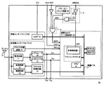
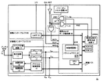
図8は、典型的な従来のICカード90の概略的構成を示すブロック図である。ICカード用LSIの内部ブロックは、演算及びデータ格納部40、非接触インタフェース10、接触インタフェース60、パワーオンリセット回路80、及びアンテナ15を備えて構成される。
FIG. 8 is a block diagram showing a schematic configuration of a typical
非接触インタフェース10は、整流回路11、変調回路12、復調回路13、クロック分離回路14、レギュレータ16、レギュレータ17、及びプロトコル制御回路18を備える。接触インタフェース60は、UART(Universal Asynchronous Receiver Transmitter)61を備える。演算及びデータ格納部40は、通常のマイクロコンピュータの構成と殆ど同じであり、CPU41、ROM42、RAM43、及びフラッシュマクロ20を備える。ROM42はプログラムを格納するものであり、RAM43はワーキングメモリとして演算中に使用される。フラッシュマクロ20はプログラムを格納、またはデータを保持するのに使用される。
The non-contact interface 10 includes a
尚、フラッシュマクロ20は、外部からの電磁波照射を検出する電磁波照射検出回路70を内部に備える。当該回路70の構成については後述する。
The flash macro 20 includes an electromagnetic wave
以下、上記構成を有する非接触型ICカード90に内装されるICモジュールの基本的動作について、図8を参照して説明する。
The basic operation of the IC module built in the non-contact
先ず、外部のリーダライタ装置(図示せず)より非接触ICカード90の制御信号が電磁波に変換されて与えられる。非接触ICカードが、当該電磁波に変換された制御信号を受信すると、非接触ICカード90内部に埋め込まれたアンテナ15において電磁誘導を生じさせる。この電磁誘導により発生した信号は、演算及びデータ格納部40を動作させるための供給電力、クロック信号、制御信号に変換される。
First, a control signal for the
又、前記電磁誘導により発生した信号は、整流回路11を介して正の電圧に変換され、更にレギュレータ16(VPPを発生)、レギュレータ17(VCCを発生)を介して平滑化され、演算及びデータ格納部40に電源電圧として供給される。尚、一般的なICモジュールの電源電圧(VCC及びVPP)は5V或いは3Vである。
Further, the signal generated by the electromagnetic induction is converted to a positive voltage through a
又、前記電磁誘導により発生した信号は、クロック分離回路14により、内部クロックに変換される。内部クロックの周波数はおよそ1MHz〜15MHzである。 The signal generated by the electromagnetic induction is converted into an internal clock by the clock separation circuit 14. The frequency of the internal clock is approximately 1 MHz to 15 MHz.
更に、前記電磁誘導により発生した信号は、復調回路13を通して、プロトコル制御回路18に入力される。プロトコル制御回路18は、非接触ICカードの通信プロトコル(例えば近傍型非接触ICカードの場合、TypeA、TypeB、TypeC)の制御、およびCPU41とデータの送受信を行う。CPU41は、前記データに基づき、ROM42、RAM43、フラッシュマクロ20を制御し演算等の処理を行う。CPU41で演算された結果は、プロトコル制御回路18を介して、変調回路12により変調され、所定の帯域を持った交流信号に変換された後、アンテナ15から電磁波として出力される。外部のリーダライタ装置はこの電磁波を受け取り、リーダライタ装置内の復調回路を通して信号に変換し、ICカードとの情報の授受を完了する。
Further, the signal generated by the electromagnetic induction is input to the
パワーオンリセット回路80は主に非接触動作におけるリセット信号を出力する回路である。ICカード90がリーダライタ装置に対して所定範囲内の距離に近接すると、リーダライタ装置から発せされる電磁波が電磁誘導されることで生成される電圧が上昇する。この電圧に基づいて生成される電源電圧VCCが所望の電圧に達した場合(例えば2.3V)、リセット状態が解除される。
The power-on reset circuit 80 is a circuit that mainly outputs a reset signal in a non-contact operation. When the
一方、外部リセット信号RSTは、接触動作時におけるリセット信号である。接触型のリーダライタ装置により制御される。電圧値が所定のレベルを下回ると外部リセット信号RSTが活性化される(ロウアクティブ)。 On the other hand, the external reset signal RST is a reset signal during the contact operation. It is controlled by a contact type reader / writer device. When the voltage value falls below a predetermined level, the external reset signal RST is activated (low active).
尚、パワーオンリセット回路80の出力信号、並びに外部リセット信号RST(の否定信号)は、共に内部で論理和回路で構成されるリセット信号生成回路9によってOR接続されている。このリセット信号生成回路9の出力信号がリセット信号RST1として演算及びデータ格納部40に与えられる。演算及びデータ格納部40は、活性状態であるリセット信号RST1が与えられると、リセット処理を実行する。リセット信号生成回路9に入力される電磁波照射検出回路70からの出力信号ERRについては後述する。
Note that the output signal of the power-on reset circuit 80 and the external reset signal RST (negative signal thereof) are both OR-connected by a reset
上述したように、近年のICカードには不揮発性半導体記憶装置が搭載されており、当該記憶装置内において種々の情報が記録されている。かかる情報には、暗証番号等の個人情報の他、秘密保持の必要性の高い情報が含まれているため、これらの情報の改ざんや漏洩等の不正目的のために外部からICカード内の当該記憶装置に対してアクセスが行われることを防止する措置を施す必要性がある。 As described above, a non-volatile semiconductor memory device is mounted on a recent IC card, and various information is recorded in the memory device. Since such information includes personal information such as personal identification numbers and other information that is highly necessary to maintain confidentiality, the information in the IC card is externally used for unauthorized purposes such as falsification or leakage of such information. There is a need to take measures to prevent access to the storage device.
ICカードに対して電磁波等の照射による回路動作の不正な解析を阻止し、内部データの漏洩、改ざん、並びに複製等の防止に関する従来の技術としては下記特許文献1に開示されているものがある。特許文献1に記載の半導体装置は、半導体基板上に形成された集積回路に対して照射される電磁波を検出するための不揮発性メモリを含む検出回路(以下、「電磁波照射検出回路」と記載)を備えており、前記不揮発性メモリの読み出した値が所定の値と一致しない場合に以降の動作を停止させるものである。以下、図面を参照して、特許文献1に記載されている電磁波照射検出回路の基本的動作について説明を行う。尚、この電磁波照射検出回路は、図8に示されている電磁波照射検出回路70に相当する。
As a conventional technique for preventing illegal analysis of circuit operation by irradiating an IC card with electromagnetic waves or the like and preventing leakage, falsification, and duplication of internal data, there is one disclosed in
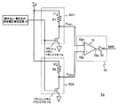
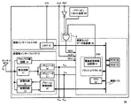
図9は、従来の電磁波照射検出回路70の概略的構成を示す回路ブロック図である。図9に示される電磁波等検出回路70は、抵抗R1、フラッシュメモリトランジスタ71、及び比較回路74を備えて構成される。
FIG. 9 is a circuit block diagram showing a schematic configuration of a conventional electromagnetic wave
抵抗R1とフラッシュメモリトランジスタ71とは、直列に配列されて直列回路を構成している。より具体的には、抵抗R1の一端に電源電圧VCCが印加され、抵抗R1の他端にフラッシュメモリトランジスタ71のドレインが接続され、フラッシュメモリトランジスタ71のソースが接地されている。尚、この電源電圧VCCは、フラッシュメモリトランジスタ71のゲートにも印加される構成である。
The resistor R1 and the
比較回路74は、コンパレータ72と否定回路73とで構成される。コンパレータ72は、反転入力端子72im、非反転入力端子72ip、及び出力端子72oを備える。反転入力端子72imには所定の基準電圧VREFが入力される。又、非反転入力端子72ipには、抵抗R1とフラッシュメモリトランジスタ71の接続ノードが示す電圧(以下、「対象電圧」と記載する)VOUTが印加される。そして、非反転入力端子72ipに入力される対象電圧VOUTと、反転入力端子72imに入力される基準電圧VREFとを比較し、その大小関係に基づく2値の電圧信号を出力端子72oから出力する。ここでは、VOUT>VREFの場合には出力端子72oから高レベル電圧(例えば3V)を出力し、逆にVOUT<VREFの場合には出力端子72oから低レベル電圧(例えば接地電圧)を出力するものとする。又、否定回路73は、コンパレータ72の出力端子72oから出力される電圧が入力され、入力電圧の高低の結果を反転し、検出信号ERRとして出力する。即ち、電磁波照射検出回路70は、VOUT>VREFの場合には検出信号ERRとして低レベル電圧(例えば接地電圧)を出力し、VOUT<VREFの場合には検出信号ERRとして高レベル電圧(例えば3V)を出力する。
The
図9に示されるような構成を有する電磁波照射検出回路70に対し、電磁波が照射されることによる対象電圧VOUTの変化について以下に説明する。
A change in the target voltage VOUT due to the electromagnetic wave irradiation to the electromagnetic wave
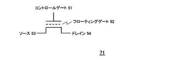
電磁波が照射されることによる対象電圧VOUTの変化を説明するに際し、先ず、フラッシュメモリトランジスタの動作原理について説明を行う。図10は、フラッシュメモリトランジスタ71の概念的な構造図である。図10に示されるように、フラッシュメモリトランジスタ71は、コントロールゲート51、フローティングゲート52、ソース53、及びドレイン54の各電極(端子)を備える。
In describing the change in the target voltage VOUT due to the irradiation of electromagnetic waves, first, the operation principle of the flash memory transistor will be described. FIG. 10 is a conceptual structural diagram of the
フラッシュメモリトランジスタ71は、フローティングゲート52内の電子の多寡によって閾値電圧が変化するため、この閾値電圧の大小によって書き込み状態と消去状態を夫々定義することで、2値或いは多値の情報の記憶が可能となる。即ち、フローティングゲート52内に蓄積されている電荷(以下、電子とする)が多い状態を書き込み状態とし、電子が蓄積されていない状態(又は蓄積されている電子が少ない状態)を消去状態とすることで、フローティングゲート52内に対して電子(ホットエレクトロン)の注入によって情報の書き込みが行われ、逆にフローティングゲート52内に蓄積されている電子が引き抜かれることで情報の消去が行われることとなる。
Since the threshold voltage of the
例えば、フラッシュメモリトランジスタ71に対して情報の書き込みを行う場合には、コントロールゲート51に高電圧(例えば12V)を、ドレイン54に高電圧(例えば7V)を、ソース53に低電圧(例えば0V)を夫々印加することで、ドレイン接合近傍で発生されたホットエレクトロンをフローティングゲート52に注入することにより行う。
For example, when information is written to the
逆に、フラッシュメモリトランジスタ71に書き込まれている情報の消去を行う場合には、コントロールゲート51に低電圧(例えば0V)を、ドレイン54に低電圧(例えば0V)を、ソース53に高電圧(例えば12V)を夫々印加し、フローティングゲート52とソース53間に高電界を発生させ、トンネル現象を利用してフローティングゲート52内の電子をソース側に引き抜くことにより行う。
On the other hand, when erasing information written in the
又、フラッシュメモリトランジスタ71から情報の読み出しを行う場合には、コントロールゲート51に高電圧(例えば5V)を、ドレイン54に低電圧(例えば1V)を、ソース53に低電圧(例えば0V)を夫々印加し、ドレイン54を流れるドレイン電流の大小を内部のセンスアンプによって増幅して、データの「1」及び「0」の判定(2値データの場合)を行う。上記電圧が印加された場合、フローティングゲート52に電子が蓄積されている(情報が書き込まれている)場合には、閾値電圧が高いため、フラッシュメモリトランジスタ71のオン抵抗が大きく、これによって前記ドレイン電流は小さくなる。逆に、フローティングゲート52に電子が蓄積されていない又は蓄積電子量が少ない(情報が消去されている)場合には、閾値電圧が低いため、フラッシュメモリトランジスタ71のオン抵抗が小さく、これによって前記ドレイン電流は大きくなる。従って、ドレイン電流の大小を検出することで、フラッシュメモリトランジスタ71の記憶状態の判別が可能となる。
When reading information from the
ICカードに備えられる不揮発性半導体記憶装置(フラッシュマクロ20)は、上述したフラッシュメモリトランジスタ71を一のメモリセルとし、かかるメモリセルを行方向並びに列方向に複数配列することで構成されたメモリセルアレイによって実現されている。図11は、図10に示すフラッシュメモリトランジスタ71をマトリクス状に配列して構成されたメモリセルアレイの概略構成図である。
A non-volatile semiconductor memory device (flash macro 20) provided in an IC card is a memory cell array configured by using the above-described
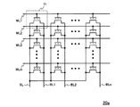
図11では、上述したフラッシュメモリトランジスタ71と同一の構成を有するトランジスタをm行n列のマトリクス状に配列したものである。図11に示されるメモリセルアレイ20aは、行方向に延伸する複数のワード線WL1、WL2、…、WLmと、列方向に延伸する複数のビット線BL1、BL2、…、BLn、及びソース線SLを備える。そして、同一行のフラッシュメモリトランジスタの各コントロールゲート夫々が同一のワード線に接続され、同一列のフラッシュメモリトランジスタの各ドレイン夫々が同一のビット線に接続され、全てのトランジスタのソースが共通のソース線SLに接続される。
In FIG. 11, transistors having the same configuration as the
このように構成されるメモリセルアレイを有するフラッシュメモリに対し、書き込み、消去、読み出し対象となるメモリセルに接続されているワード線、ビット線、並びにソース線を介して夫々処理に応じた上記電圧を印加することで、選択メモリセルに対する情報の書き込み、消去、或いは読み出しの各処理を実行する。 For the flash memory having the memory cell array configured as described above, the voltage corresponding to the processing is applied via the word line, the bit line, and the source line connected to the memory cell to be written, erased, or read. By applying this, each process of writing, erasing, or reading information on the selected memory cell is executed.
上述したような原理に基づいて情報の記憶を行うフラッシュメモリは、フローティングゲート52内に蓄積された電子の多寡によって書き込み状態と消去状態の区別を行う構成であるところ、フローティングゲート52が周囲の導電性材料と絶縁状態にある(フローティング状態にある)構成であるため、一度フローティングゲート52内に注入された電子は新たな電圧印加を行わない限り当該フローティングゲート52内に安定的に留まり、
又、新たな電圧印加を行わない限り外部の導電性材料から電子がフローティングゲート52内に注入されるようなことはなく、これによって情報を安定的に保持することができる構成である。
A flash memory that stores information based on the above-described principle is configured to distinguish between a written state and an erased state based on the number of electrons accumulated in the floating gate 52. Since the structure is in an insulating state (floating state) with the conductive material, electrons once injected into the floating gate 52 remain stably in the floating gate 52 unless a new voltage is applied,
Further, unless a new voltage is applied, electrons are not injected into the floating gate 52 from an external conductive material, and thus information can be stably held.
ところが、このようなフラッシュメモリに対して外部より電磁波が照射されると、照射された電磁波に含まれるエネルギがフローティングゲート52に与えられる結果、フローティングゲート52内に蓄積されている電子が高エネルギ状態となり、フローティングゲート52外に脱出するという事態が起こり得る。このような事態が発生すると、正しく書き込まれていた情報が不正に消去されたり、書換えられたり、或いは読み出されるという懸念が招来する。 However, when an electromagnetic wave is irradiated from the outside to such a flash memory, the energy contained in the irradiated electromagnetic wave is given to the floating gate 52, so that the electrons accumulated in the floating gate 52 are in a high energy state. Thus, a situation of escape from the floating gate 52 may occur. When such a situation occurs, there is a concern that correctly written information is illegally erased, rewritten, or read.
図9に示される電磁波照射検出回路70は、このような懸念に対処すべく、電磁波が照射された場合にフラッシュメモリセルトランジスタの閾値電圧が変化することを利用して、閾値電圧の変化を検知することで電磁波の照射を検出することを可能にするものである。
The electromagnetic wave
図9に示されるような回路構成において、電磁波が照射されていない状態(以下、「非照射状態」と記載)の下で、対象電圧VOUTが基準電圧VREFよりも大きい値(VOUT>VREF)を示すように、抵抗R1及びフラッシュメモリトランジスタ71の閾値電圧を予め設定しているものとする。この場合、上述したように、電磁波照射検出回路70から出力される検出信号ERRは低レベル電圧を示す。
In the circuit configuration shown in FIG. 9, the target voltage V OUT is larger than the reference voltage V REF (V OUT >> under a state where no electromagnetic wave is irradiated (hereinafter referred to as “non-irradiation state”). It is assumed that the threshold voltage of the resistor R1 and the
ここで、電磁波が照射されることでフローティングゲート52内に蓄積されている電子がフローティングゲート52外に脱出したとする。このとき、フラッシュメモリトランジスタ71の閾値電圧が低下し、これによってフラッシュメモリトランジスタ71のオン抵抗(以下、適宜「RON」と符号を付す)も減少する。図9に示される対象電圧VOUTは、電源電圧VCCを抵抗R1とオン抵抗RONの抵抗比で分圧することで算出される値となるため、オン抵抗RONが低下すると、抵抗R1の両端の電位差が大きくなる。この結果、抵抗R1とフラッシュメモリトランジスタ71のドレインの接続ノードの電圧で定義される対象電圧VOUTは、電源電圧VCCから抵抗R1の両端の電位差に相当する電圧が低下した値と算出できるため、かかるVOUTの値はオン抵抗RONの低下に伴って減少することとなる。
Here, it is assumed that the electrons accumulated in the floating gate 52 escape from the floating gate 52 by being irradiated with electromagnetic waves. At this time, the threshold voltage of the
ここで、電磁波が照射されることで対象電圧VOUTが基準電圧VREFを下回る程度に低下した場合、コンパレータ72の出力端子からは低レベル電圧が出力されるため、かかる信号が反転される結果、高レベル電圧の検出信号ERRが電磁波照射検出回路70から出力されることとなる。つまり、電磁波照射検出回路70からの出力される検出信号ERRが高レベル電圧であることを検出することにより、電磁波が照射されたことを認識することができる。
Here, when the target voltage V OUT is lowered to a level lower than the reference voltage V REF due to the irradiation with the electromagnetic wave, a low level voltage is output from the output terminal of the
尚、図8に示されるように、電磁波等検出回路70の出力信号であるERRは、接触動作時における外部リセット信号RSTの反転信号、並びに非接触動作時におけるリセット信号であるパワーオンリセット回路80の出力信号と共に、論理和回路で構成されるリセット信号生成回路9においてOR接続されており、このリセット信号生成回路9の出力信号がリセット信号RST1として演算及びデータ格納部40に与えられる構成である。従って、電磁波照射検出回路70によって電磁波の照射が検出された場合、高レベル電圧のERR信号がリセット信号生成回路9を介してリセット信号RST1として演算及びデータ格納部40に与えられ、これによって演算及びデータ格納部40はリセット処理が実行される。即ち、電磁波の照射を検出すると、演算及びデータ格納部40は強制的にリセット状態となるため、電磁波の照射によって内部の記録情報に対する不正な書換え、消去、或いは読み出し等が行われることを防止することができる。
As shown in FIG. 8, an ERR that is an output signal of the electromagnetic
ところが、上記従来構成においては、電源電圧VCCが変動した場合に、電磁波照射検出回路70が所望の動作を実現しない場合があった。
However, in the above-described conventional configuration, the electromagnetic wave
即ち、図9における構成において、例えば不正の目的により電源電圧VCCが仕様値よりも高く設定された場合、フラッシュメモリトランジスタ71のゲート電圧がこれに伴って高くなる。すると、フラッシュメモリトランジスタ71(を含む直列回路)を流れる電流が増加することとなり、この結果、抵抗R1の両端における電圧降下が大きくなるため、対象電圧VOUTの値は低下する。これにより、対象電圧VOUTが基準電圧VREFよりも小さい値になりやすく(VOUT<VREF)、この結果、電磁波照射検出回路70から出力される検出信号ERRは高レベルを出力しやすくなる。
That is, in the configuration in FIG. 9, for example, when the power supply voltage VCC is set higher than the specification value for an illegal purpose, the gate voltage of the
逆に、電源電圧VCCが使用値よりも低く設定された場合、フラッシュメモリトランジスタ71のゲート電圧がこれに伴って低くなるため、フラッシュメモリトランジスタ71(を含む直列回路)を流れる電流が減少し、対象電圧VOUTの値は上昇する。これにより、対象電圧VOUTが基準電圧VREFよりも大きい値になりやすく(VOUT>VREF)、この結果、電磁波照射検出回路70から出力される検出信号ERRは低レベルを出力しやすくなる。
On the contrary, when the power supply voltage VCC is set lower than the use value, the gate voltage of the
又、ICカード90は、非接触動作を行う場合、上記のように非接触型のリーダライタが発生した磁場に当該ICカードをかざすことで、電磁誘導によって発生された電力を利用して給電、クロック供給、データ通信等を行う構成である。このため、ICカード90のかざし方によっては、ICカード90とリーダタイタとの距離が変化する場合がある。ICカード90とリーダライタとの距離が離れると、磁界強度が低下し、これに伴って電流供給能力が低下してしまう。このため、消費電流が大きい動作(例えばフラッシュメモリの読み出し動作)を行うと、動作開始時には電源電圧VCCが所望の電圧に到達していても、レギュレータ17が電源電圧VCCの降下を引き起こし、この結果、前記のように電磁波照射検出回路70の誤動作を生じる場合が考えられる。
When the
又、かかる誤動作が生じると、ICカード90はリセット状態となるため、電圧の回復を待って再度読み出しを行う等の復帰処理が必要となり、重複した動作が要求される。このことはICカードの利便性を低下させるという問題を招来する。
In addition, when such a malfunction occurs, the
本発明は、上記の問題点に鑑み、電源電圧が変化した場合でも誤動作を生じることのない電磁波照射検出回路を提供することを目的とする。又、本発明は、かかる電磁波照射検出回路を備えることで、利便性を低下させることなく高セキュリティ性の実現が可能な半導体装置、並びにICカードを提供することを目的とする。 In view of the above problems, an object of the present invention is to provide an electromagnetic wave irradiation detection circuit that does not cause a malfunction even when a power supply voltage changes. It is another object of the present invention to provide a semiconductor device and an IC card that are provided with such an electromagnetic wave irradiation detection circuit and can achieve high security without deteriorating convenience.
上記目的を達成するための本発明に係る電磁波照射検出回路は、第1抵抗と第1不揮発性メモリトランジスタが直列に配列された第1直列回路と、第2抵抗と第2不揮発性メモリトランジスタが直列に配列された第2直列回路と、一対の差動入力端子の内の一方の入力端子に前記第1直列回路の前記第1抵抗と前記第1不揮発性メモリトランジスタの中間点が接続し、他方の入力端子に前記第2直列回路の前記第2抵抗と前記第2不揮発性メモリトランジスタの中間点が接続し、前記両入力端子に入力される電圧差に応じた2値の検出信号を出力する比較回路と、を備え、前記第1抵抗と前記第1不揮発性メモリトランジスタの中間点の電位、並びに前記第2直列回路の前記第2抵抗と前記第2不揮発性メモリトランジスタの中間点の電位が共に電源電圧に応じて決定される構成であり、電磁波が照射されることで所定量以上のエネルギが与えられると、前記第1及び第2不揮発性メモリトランジスタのオン抵抗が変化して、電磁波が照射されていない非照射状態と電磁波が照射された照射状態の間で、前記両入力端子に入力される電圧差が変化して、前記検出信号が変化することを第1の特徴とする。 In order to achieve the above object, an electromagnetic wave irradiation detection circuit according to the present invention includes a first series circuit in which a first resistor and a first nonvolatile memory transistor are arranged in series, a second resistor and a second nonvolatile memory transistor. An intermediate point of the first resistor of the first series circuit and the first nonvolatile memory transistor is connected to one input terminal of the second series circuit arranged in series and the pair of differential input terminals, An intermediate point of the second resistor of the second series circuit and the second nonvolatile memory transistor is connected to the other input terminal, and a binary detection signal corresponding to the voltage difference input to the two input terminals is output. A comparison circuit, and a potential at an intermediate point between the first resistor and the first nonvolatile memory transistor, and a potential at an intermediate point between the second resistor and the second nonvolatile memory transistor in the second series circuit. But The on-resistance of the first and second nonvolatile memory transistors changes when the energy of a predetermined amount or more is given by irradiation with electromagnetic waves, and the electromagnetic waves are generated. The first characteristic is that the detection signal changes between a non-irradiated state and an irradiated state in which electromagnetic waves are irradiated, in which a voltage difference inputted to both the input terminals changes.
本発明に係る電磁波照射検出回路の上記第1の特徴構成によれば、第1及び第2直列回路における所定のノード(抵抗と不揮発性メモリトランジスタの接続ノード、以下単に「中間点」と記載)の電位に基づく両電圧信号が、比較回路の両入力端子に入力され、かかる入力電圧の電圧差に基づいて検出信号が出力される。又、両直列回路は、夫々抵抗と不揮発性メモリトランジスタを有しており、電磁波が照射されることで不揮発性メモリトランジスタのオン抵抗が変化すると、直列回路を流れる電流が変化するため、前記中間点の電位が変化する構成である。このため、非照射状態の下で予め両抵抗の抵抗値、並びに両不揮発性メモリトランジスタの閾値電圧を所定の値に設定しておくことで、電磁波が照射された際に両直列回路の中間点の電位差が減少する。従って、かかる電位差の変化を検出することで、検出信号の電圧レベルが変化するため、これを確認することにより電磁波が照射されたことを認識することができる。 According to the first characteristic configuration of the electromagnetic wave irradiation detection circuit according to the present invention, a predetermined node in the first and second series circuits (a connection node between the resistor and the nonvolatile memory transistor, hereinafter simply referred to as “middle point”). Both voltage signals based on this potential are input to both input terminals of the comparison circuit, and a detection signal is output based on the voltage difference between the input voltages. Each series circuit has a resistor and a non-volatile memory transistor, and when the on-resistance of the non-volatile memory transistor changes due to irradiation with electromagnetic waves, the current flowing through the series circuit changes. In this configuration, the potential at the point changes. Therefore, by setting the resistance value of both resistors and the threshold voltage of both nonvolatile memory transistors to a predetermined value in a non-irradiated state in advance, the intermediate point between the two series circuits when the electromagnetic wave is irradiated The potential difference decreases. Therefore, since the voltage level of the detection signal changes by detecting such a change in potential difference, it can be recognized that the electromagnetic wave has been irradiated by confirming this.
そして、本特徴構成によれば、両中間点の電位が電源電圧に応じて決定される構成であるため、電源電圧が変化した場合であっても、比較回路に入力される両電圧信号の電圧差が、前記検出信号の電圧レベルを変化させる程度にまで変化することはない。このため、不正の目的で電源電圧を変更された場合や、利用状態によって電源電圧が変化した場合においても、これらの影響を受けることなく、正しく電磁波照射の検出を行うことができる。 According to this feature configuration, since the potential at both intermediate points is determined according to the power supply voltage, even if the power supply voltage changes, the voltage of both voltage signals input to the comparison circuit The difference does not change to such an extent that the voltage level of the detection signal is changed. For this reason, even when the power supply voltage is changed for an illegal purpose or when the power supply voltage changes depending on the usage state, the electromagnetic wave irradiation can be correctly detected without being affected by these effects.
又、本発明に係る電磁波照射検出回路は、上記第1の特徴構成に加えて、前記比較回路が、反転入力端子、非反転入力端子、及び出力端子を有するコンパレータを備え、前記反転入力端子が、前記第1直列回路の前記第1抵抗と前記第1不揮発性メモリトランジスタの中間点と接続され、前記非反転入力端子が、前記第2直列回路の前記第2抵抗と前記第2不揮発性メモリトランジスタの中間点と接続され、前記出力端子が、前記反転入力端子と前記非反転入力端子に入力される2電圧の大小関係に応じて決定される2値の電圧信号を出力する構成であり、前記検出信号の電圧レベルが、前記出力端子から出力される電圧信号の電圧レベルに基づいて決定され、電磁波が照射されることで所定量以上のエネルギが与えられると、前記第1及び第2不揮発性メモリトランジスタのオン抵抗が変化して、電磁波が照射されていない非照射状態と電磁波が照射された照射状態の間で、前記反転入力端子と前記非反転入力端子に入力される電圧の大小関係が変化して、前記出力端子より出力される前記検出信号が変化することを第2の特徴とする。 According to the electromagnetic wave irradiation detection circuit of the present invention, in addition to the first characteristic configuration, the comparison circuit includes a comparator having an inverting input terminal, a non-inverting input terminal, and an output terminal. The first resistor of the first series circuit is connected to an intermediate point of the first nonvolatile memory transistor, and the non-inverting input terminal is connected to the second resistor of the second series circuit and the second nonvolatile memory. It is connected to an intermediate point of a transistor, and the output terminal outputs a binary voltage signal determined according to a magnitude relationship between two voltages input to the inverting input terminal and the non-inverting input terminal, When the voltage level of the detection signal is determined based on the voltage level of the voltage signal output from the output terminal, and energy of a predetermined amount or more is given by being irradiated with electromagnetic waves, the first and 2 The on-resistance of the non-volatile memory transistor is changed, and the voltage input to the inverting input terminal and the non-inverting input terminal is changed between a non-irradiated state where no electromagnetic wave is irradiated and an irradiated state where the electromagnetic wave is irradiated. A second feature is that the detection signal output from the output terminal changes as the magnitude relationship changes.
本発明に係る電磁波照射検出回路の上記第2の特徴構成によれば、電磁波が照射されると、前記反転入力端子と前記非反転入力端子に入力される2電圧の大小関係が変化し、これによって検出信号が変化する。従って、この検出信号の電圧レベルの変化を確認することにより電磁波が照射されたことを認識することができる。 According to the second characteristic configuration of the electromagnetic wave irradiation detection circuit according to the present invention, when electromagnetic waves are irradiated, the magnitude relationship between the two voltages input to the inverting input terminal and the non-inverting input terminal changes. Changes the detection signal. Therefore, it can be recognized that the electromagnetic wave has been irradiated by confirming the change in the voltage level of the detection signal.
そして、本特徴構成によれば、両中間点の電位が電源電圧に応じて決定される構成であるため、電源電圧が変化した場合であっても、比較回路に入力される両電圧信号の大小関係が非照射状態の下での大小関係と逆転することがない。このため、不正の目的で電源電圧を変更された場合や、利用状態によって電源電圧が変化した場合においても、これらの影響を受けることなく、正しく電磁波照射の検出を行うことができる。 According to this feature configuration, since the potential at both intermediate points is determined according to the power supply voltage, the magnitude of both voltage signals input to the comparison circuit is large even when the power supply voltage changes. The relationship does not reverse with the magnitude relationship under non-irradiation conditions. For this reason, even when the power supply voltage is changed for an illegal purpose or when the power supply voltage changes depending on the usage state, the electromagnetic wave irradiation can be correctly detected without being affected by these effects.
ここで、前記比較回路が更に否定回路を備えると共に、前記コンパレータの出力端子に否定回路が接続されることで、コンパレータの出力端子から出力される信号の電圧レベルを反転させて前記検出信号を生成する構成としても良い。 Here, the comparison circuit further includes a negative circuit, and a negative circuit is connected to the output terminal of the comparator, thereby generating the detection signal by inverting the voltage level of the signal output from the output terminal of the comparator. It is good also as composition to do.
又、本発明に係る電磁波照射検出回路は、上記第2の特徴構成に加えて、前記第1抵抗の抵抗値が前記第2抵抗の抵抗値よりも小さく、前記非照射状態において、前記第1不揮発性メモリセルの閾値電圧が前記第2不揮発性メモリセルの閾値電圧よりも小さいことを第3の特徴とする In addition to the second characteristic configuration, the electromagnetic wave irradiation detection circuit according to the present invention has a resistance value of the first resistor smaller than a resistance value of the second resistor. A third feature is that a threshold voltage of the nonvolatile memory cell is smaller than a threshold voltage of the second nonvolatile memory cell.
本発明に係る電磁波照射検出回路の上記第3の特徴構成によれば、非照射状態の下では非反転入力端子に入力される電圧レベルが、反転入力端子に入力される電圧レベルよりも高くなる。そして、かかる構成の下で、電磁波が照射されると、両不揮発性メモリトランジスタの閾値電圧が共に低下するため、両直列回路を流れる電流は共に上昇する。この結果、所定量以上のエネルギが電磁波の照射によって与えられると、抵抗値が大きい第2抵抗の両端の電位差が、抵抗値の小さい第1抵抗の両端の電位差を上回り、両入力端子に入力される電圧レベルの大小関係が逆転し、検出信号の電圧レベルもこれに応じて変化する。従って、出力される検出信号の電圧レベルの変化を確認することで、電磁波が照射されたことを認識することができる。 According to the third characteristic configuration of the electromagnetic wave irradiation detection circuit according to the present invention, the voltage level input to the non-inverting input terminal is higher than the voltage level input to the inverting input terminal under the non-irradiation state. . Under such a configuration, when electromagnetic waves are irradiated, both the threshold voltages of both nonvolatile memory transistors are lowered, so that both currents flowing through both series circuits are increased. As a result, when energy of a predetermined amount or more is given by irradiation of electromagnetic waves, the potential difference between both ends of the second resistor having a large resistance value exceeds the potential difference between both ends of the first resistor having a small resistance value, and is input to both input terminals. The magnitude relationship between the voltage levels is reversed, and the voltage level of the detection signal also changes accordingly. Therefore, it is possible to recognize that the electromagnetic wave has been irradiated by confirming the change in the voltage level of the output detection signal.
又、本発明に係る電磁波照射検出回路は、上記第2又は第3の特徴構成に加えて、所定領域に電磁波遮蔽手段を備えており、前記電磁波遮蔽手段によって照射された電磁波の一部が反射されることで、前記第1不揮発性メモリトランジスタに対して与えられるエネルギ量が前記第2不揮発性メモリトランジスタに対して与えられるエネルギ量よりも少なくなるように構成されていることを第4の特徴とする。 In addition to the second or third feature configuration, the electromagnetic wave irradiation detection circuit according to the present invention further includes an electromagnetic wave shielding means in a predetermined area, and a part of the electromagnetic wave irradiated by the electromagnetic wave shielding means is reflected. Thus, the fourth feature is that the amount of energy given to the first nonvolatile memory transistor is smaller than the amount of energy given to the second nonvolatile memory transistor. And
本発明に係る電磁波照射検出回路の上記第4の特徴構成によれば、両不揮発性メモリトランジスタに対して電磁波が照射された場合であっても、当該照射によって両不揮発性トランジスタに与えられるエネルギ量に差異が生じる。この結果、両不揮発性メモリトランジスタ間の閾値電圧の変化に差異を設けることができる。従って、非照射状態の下で中間点の電位が低く設定されている側の直列回路が有する不揮発性メモリトランジスタを、他の不揮発性メモリトランジスタよりも電磁波の遮蔽能力を高く設定しておくことで、電磁波が照射されると比較回路の両入力端子に入力される両入力電圧の大小関係が逆転するため、検出信号の電圧レベルが変化し、これによって電磁波の照射を検出することができる。 According to the fourth characteristic configuration of the electromagnetic wave irradiation detection circuit according to the present invention, even when electromagnetic waves are irradiated to both nonvolatile memory transistors, the amount of energy given to both nonvolatile transistors by the irradiation There will be a difference. As a result, a difference can be provided in the change in threshold voltage between the two nonvolatile memory transistors. Therefore, the non-irradiation state of the non-volatile memory transistor of the series circuit on the side where the potential at the intermediate point is set low is set higher than the other non-volatile memory transistors. When the electromagnetic wave is irradiated, the magnitude relationship between the two input voltages input to both input terminals of the comparison circuit is reversed, so that the voltage level of the detection signal is changed, thereby detecting the electromagnetic wave irradiation.
尚、電磁波の遮蔽能力を高く設定したい側の不揮発性メモリトランジスタに対してのみ電磁波遮蔽手段を備える構成としても構わないし、例えば遮蔽面積や遮蔽部材に差異を設けることで両不揮発性メモリトランジスタに対して電磁波遮蔽手段を備える構成としても構わない。 The electromagnetic wave shielding means may be provided only for the nonvolatile memory transistor on the side where the electromagnetic wave shielding capability is desired to be set high. For example, by providing a difference in the shielding area and the shielding member, The electromagnetic wave shielding means may be provided.
又、本特徴構成の場合には、電磁波の照射によって両不揮発性メモリトランジスタの閾値電圧の変化程度が異なるため、第1及び第2抵抗の抵抗値を同一値とした場合であっても、電磁波が照射されることで比較回路に入力される両入力電圧の大小関係を変化させることができる。 In the case of this characteristic configuration, the degree of change in the threshold voltage of both nonvolatile memory transistors differs depending on the irradiation of electromagnetic waves, so that even when the resistance values of the first and second resistors are the same, , The magnitude relationship between the two input voltages input to the comparison circuit can be changed.
又、本発明に係る電磁波照射検出回路は、上記第4の特徴構成に加えて、前記電磁波遮蔽手段が、前記第1不揮発性メモリセルの形成領域の上層に備えられており、前記第2不揮発性メモリセルの形成領域の上層に備えられていないことを第5の特徴とする。 According to the electromagnetic wave irradiation detection circuit of the present invention, in addition to the fourth characteristic configuration, the electromagnetic wave shielding means is provided in an upper layer of the formation area of the first nonvolatile memory cell, and the second nonvolatile memory is provided. The fifth feature is that it is not provided in the upper layer of the formation region of the memory cell.
又、本発明に係る電磁波照射検出回路は、上記第4又は第5の特徴構成に加えて、前記電磁波遮蔽手段が金属配線層で構成されることを第6の特徴とする。 In addition to the fourth or fifth characteristic configuration, the electromagnetic wave irradiation detection circuit according to the present invention has a sixth characteristic that the electromagnetic wave shielding means is formed of a metal wiring layer.
又、本発明に係る電磁波照射検出回路は、上記第1〜第6の何れか一の特徴構成に加えて、前記第1直列回路と前記第2直列回路が並列に接続されており、夫々の一方の端子には第1基準電圧が、他方の端子には第2基準電圧が印加され、前記第1基準電圧が、電源電圧、又は当該電源電圧に応じて決定される電圧であり、前記第1不揮発性メモリトランジスタ及び前記第2不揮発性メモリトランジスタの両コントロールゲートに対して、前記第1基準電圧が印加される構成であることを第7の特徴とする。 Further, in the electromagnetic wave irradiation detection circuit according to the present invention, the first series circuit and the second series circuit are connected in parallel in addition to any one of the first to sixth feature configurations, A first reference voltage is applied to one terminal, a second reference voltage is applied to the other terminal, and the first reference voltage is a power supply voltage or a voltage determined according to the power supply voltage. A seventh feature is that the first reference voltage is applied to both control gates of the first nonvolatile memory transistor and the second nonvolatile memory transistor.
本発明に係る電磁波照射検出回路の上記第7の特徴構成によれば、両直列回路の両端は夫々同一の電位を示すため、電源電圧が変化した場合には、当該変化に応じて両直列回路の中間点の電位が同様の変化を示すこととなる。即ち、電源電圧の変化によって中間点の電位の大小関係が変化することがないため、誤動作を生じることなく正しく電磁波照射の検出を実行することができる。 According to the seventh characteristic configuration of the electromagnetic wave irradiation detection circuit according to the present invention, both ends of both series circuits exhibit the same potential, so that when the power supply voltage changes, both series circuits correspond to the change. That is, the potential at the intermediate point of FIG. That is, since the magnitude relation of the potential at the intermediate point does not change due to the change in the power supply voltage, the electromagnetic wave irradiation can be correctly detected without causing a malfunction.
尚、前記第2基準電圧は、例えば接地電圧とすることができる。 The second reference voltage can be a ground voltage, for example.
又、本発明に係る電磁波照射検出回路は、上記第1〜第6の何れか一の特徴構成に加えて、前記第1直列回路と前記第2直列回路が並列に接続されており、夫々の一方の端子には第1基準電圧が、他方の端子には第2基準電圧が印加され、前記第1基準電圧が、電源電圧、又は当該電源電圧に応じて決定される電圧であり、前記第1不揮発性メモリトランジスタ及び前記第2不揮発性メモリトランジスタの両コントロールゲートに対して、前記第1或いは第2不揮発性メモリトランジスタに対する読み出し、書き込み、或いは消去処理を行うための電圧発生回路からの出力電圧が印加されることを第8の特徴とする。 Further, in the electromagnetic wave irradiation detection circuit according to the present invention, the first series circuit and the second series circuit are connected in parallel in addition to any one of the first to sixth feature configurations, A first reference voltage is applied to one terminal, a second reference voltage is applied to the other terminal, and the first reference voltage is a power supply voltage or a voltage determined according to the power supply voltage. An output voltage from a voltage generation circuit for performing read, write, or erase processing on the first or second nonvolatile memory transistor with respect to both control gates of the first nonvolatile memory transistor and the second nonvolatile memory transistor The eighth characteristic is that is applied.
本発明に係る電磁波照射検出回路の上記第8の特徴構成によれば、両不揮発性メモリトランジスタのフローティングゲートに蓄積される電子量を多くすることができるため、閾値電圧を上昇させることができる。これにより、電磁波が照射されたときの閾値電圧並びに両直流回路を流れる電流に対する影響を大きくすることができるため、電磁波照射の検出精度を高めることができる。 According to the eighth characteristic configuration of the electromagnetic wave irradiation detection circuit according to the present invention, the amount of electrons stored in the floating gates of both the nonvolatile memory transistors can be increased, so that the threshold voltage can be increased. Thereby, since the influence with respect to the threshold voltage when an electromagnetic wave is irradiated and the electric current which flows through both DC circuits can be enlarged, the detection accuracy of an electromagnetic wave irradiation can be improved.
又、本発明に係る電磁波照射検出回路は、上記第1〜第8の何れか一の特徴構成に加えて、前記第1及び第2不揮発性メモリトランジスタのソース・ドレイン端子間にバイアス電圧を印加するためのバイアス発生回路を備えることを第9の特徴とする。 The electromagnetic wave irradiation detection circuit according to the present invention applies a bias voltage between the source and drain terminals of the first and second nonvolatile memory transistors in addition to any one of the first to eighth characteristic configurations. It is a ninth feature that a bias generation circuit is provided.
本発明に係る電磁波照射検出回路の上記第9の特徴構成によれば、非照射状態の下では両不揮発性メモリトランジスタのドレイン・ソース間に所定のバイアス電圧が印加されるように構成することができるため、かかるバイアス電圧を予め低い電圧に設定しておくことにより、非照射状態の下でソフトプログラム(弱い書き込み)が発生するのを防止することができる。これにより、非照射状態の下で各不揮発性メモリトランジスタのフローティングゲート内に蓄積されている電子量の変動を防止され、電磁波照射検出精度を更に向上させることができる。 According to the ninth characteristic configuration of the electromagnetic wave irradiation detection circuit according to the present invention, it is configured that a predetermined bias voltage is applied between the drain and the source of both nonvolatile memory transistors under the non-irradiation state. Therefore, by setting the bias voltage to a low voltage in advance, it is possible to prevent a soft program (weak writing) from occurring under a non-irradiation state. As a result, fluctuations in the amount of electrons accumulated in the floating gate of each nonvolatile memory transistor under non-irradiation conditions can be prevented, and electromagnetic wave irradiation detection accuracy can be further improved.
又、本発明に係る電磁波照射検出回路は、上記第1〜第9の何れか一の特徴構成に加えて、前記第1及び第2不揮発性メモリトランジスタがフラッシュメモリトランジスタで構成されることを第10の特徴とする。 According to the electromagnetic wave irradiation detection circuit of the present invention, in addition to any one of the first to ninth characteristic configurations, the first and second nonvolatile memory transistors are configured by flash memory transistors. Ten features.
又、本発明に係る電磁波照射検出回路は、上記第1〜第10の何れか一の特徴構成に加えて、前記第1及び第2不揮発性メモリトランジスタが、ゲート及びドレインに金属配線層との接続を構成しており、前記第1不揮発性メモリトランジスタのゲート端子及びドレイン端子に接続されている金属配線層の面積と、前記第2不揮発性メモリトランジスタのゲート端子及びドレイン端子に接続されている金属配線層の面積と、が異なっていることを第11の特徴とする。 According to the electromagnetic wave irradiation detection circuit of the present invention, in addition to any one of the first to tenth characteristic configurations, the first and second nonvolatile memory transistors may include a metal wiring layer at a gate and a drain. The area of the metal wiring layer connected to the gate terminal and the drain terminal of the first nonvolatile memory transistor and the gate terminal and the drain terminal of the second nonvolatile memory transistor. The eleventh feature is that the area of the metal wiring layer is different.
上記第11の特徴構成を有する本発明に係る電磁波照射検出回路を製造する際、ゲート電極並びにドレイン拡散層に対して金属配線層を接続させることで、この金属配線層を堆積する際に、当該金属配線層内に電荷が蓄積されることとなる。このため、製造された本発明に係る電磁波照射検出回路が有する両不揮発性メモリトランジスタに対して書き込み処理を行うと、金属配線層内に蓄積されていた電荷もフローティングゲート内に取り込まれるため、金属配線層を有しない構成と比較して閾値電圧を変化させることができる。 When manufacturing the electromagnetic wave irradiation detection circuit according to the present invention having the eleventh feature configuration, the metal wiring layer is connected to the gate electrode and the drain diffusion layer, and when the metal wiring layer is deposited, Charges are accumulated in the metal wiring layer. For this reason, when writing processing is performed on both nonvolatile memory transistors included in the manufactured electromagnetic wave irradiation detection circuit according to the present invention, the charge accumulated in the metal wiring layer is also taken into the floating gate. The threshold voltage can be changed as compared with a configuration having no wiring layer.
ゲート電極並びにドレイン拡散層に対して接続されている金属配線層の配線量(配線長、配線面積)が多いほど、当該金属配線層内に取り込まれる電子量は増大するため、かかる配線量を第1及び第2不揮発性メモリトランジスタ間で差異を持たせることにより、予め両不揮発性メモリトランジスタ間の閾値電圧に差異を生じさせることができる。即ち、本特徴構成によれば、製造された時点で既に両不揮発性メモリトランジスタの閾値電圧の調整がされているため、改めて閾値電圧の調整を行う必要がない。このため、本発明に係る電磁波照射検出回路を半導体装置内に実装する際において、当該半導体装置は、両不揮発性メモリトランジスタの閾値電圧の調整のための調整手段を設ける必要がなく、装置規模の縮小化の実現に寄与することができる。 As the amount of wiring (wiring length, wiring area) of the metal wiring layer connected to the gate electrode and the drain diffusion layer increases, the amount of electrons taken into the metal wiring layer increases. By making a difference between the first and second nonvolatile memory transistors, it is possible to cause a difference in the threshold voltage between the two nonvolatile memory transistors in advance. That is, according to this characteristic configuration, since the threshold voltages of both nonvolatile memory transistors have already been adjusted at the time of manufacture, there is no need to adjust the threshold voltage again. For this reason, when the electromagnetic wave irradiation detection circuit according to the present invention is mounted in a semiconductor device, the semiconductor device does not need to be provided with an adjusting means for adjusting the threshold voltage of both nonvolatile memory transistors, and the scale of the device is large. It can contribute to realization of reduction.
又、上記目的を達成するための本発明に係る半導体装置は、上記第1〜第11の何れか一の特徴構成の電磁波照射検出回路と、前記比較回路から出力される前記検出信号の活性/不活性状態に基づいて、リセット信号を生成するリセット信号生成回路と、を備え、前記リセット信号生成回路から出力される前記リセット信号に基づいてリセット動作が行われることを第1の特徴とする。 In order to achieve the above object, a semiconductor device according to the present invention includes an electromagnetic wave irradiation detection circuit having any one of the first to eleventh characteristic configurations, and an activity / activity of the detection signal output from the comparison circuit. A reset signal generation circuit for generating a reset signal based on an inactive state, and a reset operation is performed based on the reset signal output from the reset signal generation circuit.
本発明に係る半導体装置の上記第1の特徴構成によれば、電源電圧の変動の影響を受けることなく電磁波照射の検出を行うことができる電磁波照射検出回路を備える構成であるため、電源電圧の変動によって電磁波照射検出回路が誤動作してリセット処理が実行されるということがない。従って、電源電圧の変動によって当該リセット処理後の復帰処理を要求されることがないため、利便性を低下させることなくセキュリティ性の高い半導体装置の実現が可能となる。 According to the first characteristic configuration of the semiconductor device according to the present invention, the configuration includes the electromagnetic wave irradiation detection circuit that can detect the electromagnetic wave irradiation without being affected by the fluctuation of the power source voltage. There is no possibility that the electromagnetic wave irradiation detection circuit malfunctions due to fluctuations and the reset process is executed. Accordingly, since a return process after the reset process is not required due to fluctuations in the power supply voltage, a highly secure semiconductor device can be realized without deteriorating convenience.
又、上記目的を達成するための本発明に係る半導体装置は、上記第1〜第11の何れか一の特徴構成の電磁波照射検出回路と、前記比較回路から出力される前記検出信号の活性/不活性状態に基づいて、リセット信号を生成するリセット信号生成回路と、前記電磁波照射検出回路の検出結果の無効化処理が可能な無効化回路と、を備えると共に、前記リセット信号生成回路から出力される前記リセット信号に基づいてリセット動作が行われる構成であって、前記無効化回路が、前記電磁波照射検出回路の検出結果の無効化処理を実行するか否かの指示を示す無効化指示信号と前記検出信号とが入力される構成であって、前記無効化処理を実行しない旨の前記無効化指示信号が入力されている場合には、前記検出信号を前記リセット信号生成回路に入力し、前記無効化処理を実行する旨の前記無効化指示信号が入力されている場合には、前記検出信号の活性/不活性に拘らず、不活性状態を示す電圧信号を前記リセット信号生成回路に入力することを第2の特徴とする。 In order to achieve the above object, a semiconductor device according to the present invention includes an electromagnetic wave irradiation detection circuit having any one of the first to eleventh characteristic configurations, and an activity / activity of the detection signal output from the comparison circuit. A reset signal generation circuit that generates a reset signal based on an inactive state; and an invalidation circuit that can invalidate a detection result of the electromagnetic wave irradiation detection circuit, and is output from the reset signal generation circuit. A reset operation is performed based on the reset signal, the invalidation instruction signal indicating an instruction as to whether or not the invalidation circuit executes invalidation processing of the detection result of the electromagnetic wave irradiation detection circuit; When the invalidation instruction signal indicating that the invalidation processing is not performed is input, the detection signal is input to the reset signal generation circuit. When the invalidation instruction signal for executing the invalidation process is input, a voltage signal indicating an inactive state is supplied to the reset signal regardless of activation / inactivation of the detection signal. The second feature is to input to the generation circuit.
本発明に係る半導体装置の上記第2の特徴構成によれば、本発明に係る電磁波照射検出回路の検出結果を無効化することができる。このため、電磁波照射検出回路が備える不揮発性メモリトランジスタの閾値電圧が所定の条件を充足せず、非照射状態下においても電磁波の照射を検出した旨の検出信号を出力してしまう場合に、当該無効化処理を実行して、電磁波照射検出回路の検出結果を無効化した上で、電磁波照射検出の機能を奏するように両不揮発性メモリトランジスタの閾値電圧を調整することができる。 According to the second characteristic configuration of the semiconductor device according to the present invention, the detection result of the electromagnetic wave irradiation detection circuit according to the present invention can be invalidated. For this reason, the threshold voltage of the nonvolatile memory transistor included in the electromagnetic wave irradiation detection circuit does not satisfy the predetermined condition, and the detection signal indicating that the electromagnetic wave irradiation is detected even in the non-irradiation state is output. The threshold voltage of both nonvolatile memory transistors can be adjusted so as to perform the function of electromagnetic wave irradiation detection after executing the invalidation process to invalidate the detection result of the electromagnetic wave irradiation detection circuit.
又、本発明に係る半導体装置は、上記第2の特徴構成に加えて、前記無効化回路が、外部からテストパッドにより前記無効化指示信号の入力受付を可能に構成されていることを第3の特徴とする。 According to a third aspect of the present invention, in addition to the second feature configuration, the invalidation circuit is configured such that the invalidation instruction signal can be received from the outside by a test pad. It is characterized by.
本発明に係る半導体装置の上記第3の特徴構成によれば、不揮発性メモリトランジスタの閾値電圧の調整の際、簡易な処理によって電磁波照射検出回路の検出結果の無効化を実行することができる。 According to the third characteristic configuration of the semiconductor device of the present invention, the detection result of the electromagnetic wave irradiation detection circuit can be invalidated by a simple process when adjusting the threshold voltage of the nonvolatile memory transistor.
又、本発明に係る半導体装置は、上記第2の特徴構成に加えて、一定の動作条件が充足されると高レベルの動作リセット指示信号を出力する動作リセット回路と、2値の電圧レベルの前記無効化指示信号を生成し、前記無効化回路に対して出力する無効化指示信号生成回路と、を備え、前記リセット信号生成回路が、前記無効化回路の出力信号と前記動作リセット指示信号とが入力されると共に、何れか一の信号が活性状態であるか否かに基づいて前記リセット信号を生成する構成であり、前記無効化指示信号生成回路が、所定の無効化指示用不揮発性メモリトランジスタの記憶状態に応じた高低2値の無効化副指示信号、並びに前記動作リセット指示信号が入力されると共に、当該入力される電圧レベルの高低に応じた2値の一時記憶情報を記憶可能な構成であって、記憶している前記一時記憶情報と異なる情報に対応付けられた電圧レベルの前記無効化指示信号を出力することを第4の特徴とする。 In addition to the second characteristic configuration, the semiconductor device according to the present invention includes an operation reset circuit that outputs a high level operation reset instruction signal when a certain operation condition is satisfied, and a binary voltage level. An invalidation instruction signal generation circuit that generates the invalidation instruction signal and outputs the invalidation instruction signal to the invalidation circuit, wherein the reset signal generation circuit includes the output signal of the invalidation circuit, the operation reset instruction signal, Is input, and the reset signal is generated based on whether any one of the signals is in an active state, and the invalidation instruction signal generation circuit has a predetermined invalidation instruction nonvolatile memory. Temporary binary storage information corresponding to the level of the input voltage level is input together with a high / low binary invalidation sub-instruction signal corresponding to the storage state of the transistor and the operation reset instruction signal. A storable configuration, the fourth being to output the invalidation instruction signal voltage level associated with the temporary storage information different from information stored.
本発明に係る半導体装置の上記第4の特徴構成によれば、無効化指示用不揮発性メモリトランジスタの記憶状態に応じて無効化処理を実行するか否かを決定することができる。このため、パッケージ等にアセンブリする前段階において、無効化指示用不揮発性メモリトランジスタに対して、無効化処理が実行される状態を示す記憶状態にしておき、閾値電圧の調整後、当該無効化指示用不揮発性メモリトランジスタの記憶状態を再度変化させて、無効化処理を実行しない旨の記憶状態に変化させることができる。不揮発性メモリトランジスタの記憶状態の変化、並びに当該記憶状態の読み出しは、通常の不揮発性半導体記憶装置の書き込み、消去、読み出しの各処理で実行が可能であるため、予めプログラム化することが可能である。従って、本特徴構成によれば、電磁波照射検出回路からの検出結果の無効化と有効化の切換を自動的に行うことができる。 According to the fourth characteristic configuration of the semiconductor device according to the present invention, it is possible to determine whether or not to execute the invalidation process according to the storage state of the invalidation instruction nonvolatile memory transistor. For this reason, before the assembly into a package or the like, the invalidation instruction nonvolatile memory transistor is set in a storage state indicating a state in which the invalidation process is executed, and after the threshold voltage is adjusted, the invalidation instruction is performed. The storage state of the non-volatile memory transistor can be changed again to change to a storage state indicating that the invalidation process is not executed. The change in the storage state of the nonvolatile memory transistor and the reading of the storage state can be executed in the writing, erasing, and reading processes of a normal nonvolatile semiconductor memory device, and can be programmed in advance. is there. Therefore, according to this characteristic configuration, it is possible to automatically switch between invalidation and validation of the detection result from the electromagnetic wave irradiation detection circuit.
又、上記目的を達成するための本発明に係るICカードは、上記第1〜第4の何れか一の特徴構成の半導体装置と、非接触型外部装置と非接触で通信されることで情報の授受が行われると共に前記非接触型外部装置から電磁結合によって電力が供給される非接触型通信インタフェース、或いは、接触型外部装置との接触によって情報の授受が行われると共に前記接触型外部装置から電力が供給される接触型通信インタフェースの内の何れか一方又は双方を備えることを特徴とする。 In order to achieve the above object, the IC card according to the present invention communicates in a non-contact manner with the semiconductor device having any one of the first to fourth characteristic configurations and the non-contact type external device. Is exchanged, and information is exchanged by contact with the contact-type external device and power is supplied from the non-contact-type external device by electromagnetic coupling. One or both of contact-type communication interfaces to which power is supplied are provided.
本発明に係るICカードの上記特徴構成によれば、電源電圧の変動によって強制的にリセット処理が実行されることがないため、誤動作によって生じたリセット処理後の復帰処理を要求されることがなく、これによって、利便性の低下をさせることなくセキュリティ性の高いICカードを実現することが可能となる。 According to the above characteristic configuration of the IC card according to the present invention, the reset process is not forcibly executed due to the fluctuation of the power supply voltage, so that the return process after the reset process caused by the malfunction is not required. As a result, an IC card with high security can be realized without reducing convenience.
本発明の構成によれば、電源電圧が変化した場合でも誤動作を生じることのない電磁波照射検出回路を実現することができる。又、本発明に係る電磁波照射検出回路を備えることで、利便性を低下させることなく高セキュリティ性の実現が可能な半導体装置を実現することができる。 According to the configuration of the present invention, it is possible to realize an electromagnetic wave irradiation detection circuit that does not cause a malfunction even when the power supply voltage changes. In addition, by providing the electromagnetic wave irradiation detection circuit according to the present invention, a semiconductor device capable of realizing high security without reducing convenience can be realized.
以下において、本発明に係る電磁波照射検出回路(以下、適宜「本発明回路」と称する)、本発明に係る半導体装置(以下、適宜「本発明装置」と称する)の各実施形態について図面を参照して説明する。 In the following, referring to the drawings, each embodiment of an electromagnetic wave irradiation detection circuit according to the present invention (hereinafter referred to as “the present circuit” as appropriate) and a semiconductor device according to the present invention (hereinafter referred to as “the present apparatus” as appropriate) To explain.
尚、以下の各実施形態において、図8〜図11を参照して上述した従来技術と同一の構成については、同一の符号を付して、その詳細な説明を省略する。 In the following embodiments, the same components as those in the prior art described above with reference to FIGS. 8 to 11 are denoted by the same reference numerals, and detailed description thereof is omitted.
《本発明回路の構成》
先ず、本発明回路の各実施形態につき、以下に説明する。
<< Configuration of the Circuit of the Present Invention >>
First, each embodiment of the circuit of the present invention will be described below.
[第1実施形態]
本発明回路の第1実施形態(以下、適宜「本実施形態」と称する)につき、図1及び図2を参照して説明する。
[First Embodiment]
A first embodiment of the circuit of the present invention (hereinafter referred to as “this embodiment” as appropriate) will be described with reference to FIGS.
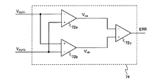
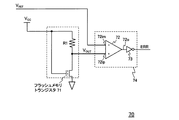
図1は、本実施形態における本発明回路の概略的構成を示す回路ブロック図である。本発明回路1は、図9に示される従来の電磁波照射検出回路70と比較して、抵抗とフラッシュメモリトランジスタからなる直列回路を2回路有する点が異なる。
FIG. 1 is a circuit block diagram showing a schematic configuration of a circuit of the present invention in this embodiment. The
即ち、本発明回路1は、抵抗R1とフラッシュメモリトランジスタ71aとが直列に配列されて構成される直列回路SC1、及び、抵抗R2とフラッシュメモリトランジスタ71bとが直列に配列されて構成される直列回路SC2、の2つの直列回路を有する構成である。尚、以下において、抵抗R1、フラッシュメモリトランジスタ71a、直列回路SC1を夫々、「第1抵抗R1」、「第1フラッシュメモリトランジスタ71a」、「第1直列回路SC1」と称し、抵抗R2、フラッシュメモリトランジスタ71b、直列回路SC2を夫々、「第2抵抗R2」、「第2フラッシュメモリトランジスタ71b」、「第2直列回路SC2」と称する。又、記号が増加することによる煩雑さを回避すべく、各抵抗に付されている符号(R1、R2)がそのまま当該抵抗の抵抗値を示しているものとして説明する。
That is, the
尚、第1抵抗R1と第2抵抗R2は、同一の構造で抵抗値のみが異なる(R1≠R2)ものとし、第1フラッシュメモリトランジスタ71aと第2フラッシュメモリトランジスタ71bは、同一の構造で閾値電圧のみが異なるものとする。 The first resistor R1 and the second resistor R2 have the same structure and differ only in the resistance value (R1 ≠ R2), and the first flash memory transistor 71a and the second flash memory transistor 71b have the same structure and threshold values. Only the voltage is different.
第1直列回路SC1、及び第2直列回路SC2は、夫々一端に接地電圧が、他端に電源電圧VCCが印加されており、両者は並列接続を構成している。第1直列抵抗SC1を例にとれば、第1抵抗R1の一端に電源電圧VCCが印加され、第1抵抗R1の他端に第1フラッシュメモリトランジスタ71aのドレイン端子が接続され、第1フラッシュメモリトランジスタ71aのソース端子が接地されている。又、図9の構成と同様、第1フラッシュメモリトランジスタ71aのゲート電極には電源電圧VCCが印加される。第2直列回路SC2においても同様とする。 Each of the first series circuit SC1 and the second series circuit SC2 has a ground voltage applied to one end and a power supply voltage VCC applied to the other end, and the both constitute a parallel connection. Taking the first series resistor SC1 as an example, the power supply voltage VCC is applied to one end of the first resistor R1, the drain terminal of the first flash memory transistor 71a is connected to the other end of the first resistor R1, and the first flash The source terminal of the memory transistor 71a is grounded. Similarly to the configuration of FIG. 9, the power supply voltage VCC is applied to the gate electrode of the first flash memory transistor 71a. The same applies to the second series circuit SC2.
又、本発明回路1は、図9に示される従来の電磁波照射検出回路70と比較して、コンパレータ72の入力端子に入力される電圧が異なる。即ち、図1に示されるように、本発明回路1が備えるコンパレータ72は、第1直列回路SC1における第1抵抗R1と第1フラッシュメモリトランジスタ71aの接続ノードが示す電圧(以下、「第1対象電圧」と記載する)VOUT1が反転入力端子72imに入力され、第2直列回路SC2における第2抵抗R2と第2フラッシュメモリトランジスタ71bの接続ノードが示す電圧(以下、「第2対象電圧」と記載する)VOUT2が非反転入力端子72ipに入力される構成である。即ち、コンパレータ72の一方の入力端子に基準電圧VREFが入力されない構成である。
The
上記接続関係の下では、第1対象電圧VOUT1と第2対象電圧VOUT2の大小関係によって検出信号ERRのレベルが決定される。即ち、本発明回路1は、VOUT1<VOUT2の場合には検出信号ERRとして低レベル電圧(例えば接地電圧)を出力し、VOUT1>VOUT2の場合には検出信号ERRとして高レベル電圧(例えば3V)を出力する。
Under the above connection relation, the level of the detection signal ERR is determined by the magnitude relation between the first target voltage V OUT1 and the second target voltage V OUT2 . That is, the
第1対象電圧VOUT1と第2対象電圧VOUT2の何れかが大きい電圧値となるかは、各抵抗R1及びR2の抵抗値、並びに各フラッシュメモリトランジスタ71a及び71bの閾値電圧に依存する。ここで、両抵抗R1及びR2がR1<R2の関係を有するものとし、非照射状態の下、VOUT1<VOUT2となるように、各フラッシュメモリトランジスタ71a及び71bの閾値電圧が設定されているものとする。即ち、第1フラッシュメモリトランジスタ71aの閾値電圧をVth1とし、第2フラッシュメモリトランジスタ71bの閾値電圧をVth2とすると、非照射状態の下で、少なくともVth1<Vth2が成立しているものとする。このとき、本発明回路1は、非照射状態の下では低レベル電圧を出力しており、電磁波照射を検出していない旨の信号を出力していることとなる。
Whether one of the first target voltage V OUT1 and the second target voltage V OUT2 has a large voltage value depends on the resistance values of the resistors R1 and R2 and the threshold voltage of the flash memory transistors 71a and 71b. Here, it is assumed that both resistors R1 and R2 have a relationship of R1 <R2, and the threshold voltages of the flash memory transistors 71a and 71b are set so that V OUT1 <V OUT2 in a non-irradiation state. Shall. That is, when the threshold voltage of the first flash memory transistor 71a is V th1 and the threshold voltage of the second flash memory transistor 71b is V th2 , at least V th1 <V th2 is established under the non-irradiation state. And At this time, the
このような構成下で、本発明回路1に対して電磁波が照射された場合について検討する。上述したように、フラッシュメモリトランジスタに対して紫外線が照射されると、閾値電圧が低下する。しかし、この閾値電圧は、ある一定の値(例えば2V、以下適宜「最小閾値電圧」と称する)を境としてそれ以下には低下しなくなる。即ち、両フラッシュメモリトランジスタ71a、71bに対して電磁波が照射された場合、何れの閾値電圧も当該電磁波照射に伴って低下するものの、所定量以上の照射がされた段階で、閾値電圧の低下が見られなくなる。ここで、上述したように、両フラッシュメモリトランジスタ71a及び71bを同一の構造で構成しているため、両フラッシュメモリトランジスタの最小閾値電圧は略同程度の値を示すこととなる。
The case where electromagnetic waves are irradiated to the
従って、電磁波の照射に伴って、両フラッシュメモリトランジスタの閾値電圧が低下していくと、非照射状態の下で予め閾値電圧を低く設定されていた第1フラッシュメモリトランジスタ71aの閾値電圧が、第2フラッシュメモリトランジスタ71bの閾値電圧よりも先に前記最小閾値電圧近傍の値になる。閾値電圧が最小閾値電圧に近付くに連れ、閾値電圧の低下速度は遅くなるため、徐々に第1フラッシュメモリトランジスタ71aの閾値電圧の低下速度は、第2フラッシュメモリトランジスタ71bの低下速度と比べて遅くなる。この結果、両フラッシュメモリトランジスタの閾値電圧の差が徐々に縮まってくる。 Therefore, when the threshold voltage of both flash memory transistors decreases with the irradiation of the electromagnetic wave, the threshold voltage of the first flash memory transistor 71a, which has been set low in advance under the non-irradiation state, becomes the first threshold voltage. The value becomes near the minimum threshold voltage before the threshold voltage of the two flash memory transistor 71b. As the threshold voltage approaches the minimum threshold voltage, the threshold voltage decreases at a slower rate. Therefore, the threshold voltage of the first flash memory transistor 71a gradually decreases than the second flash memory transistor 71b. Become. As a result, the difference between the threshold voltages of both flash memory transistors is gradually reduced.
上述したように、フラッシュメモリトランジスタの閾値電圧が低下すると、オン抵抗が減少するため、ドレイン電流、即ち各直列回路を流れる電流が上昇する。そして、第1フラッシュメモリトランジスタ71aの閾値電圧が最小閾値電圧に近付くに連れ、第1直列回路SC1を流れる電流(以下、「第1電流I1」と記載)の上昇速度は第2直列回路SC2を流れる電流(以下、「第2電流I2」と記載)の上昇速度よりも遅くなる。 As described above, when the threshold voltage of the flash memory transistor is lowered, the on-resistance is reduced, so that the drain current, that is, the current flowing through each series circuit increases. Then, as the threshold voltage of the first flash memory transistor 71a approaches the minimum threshold voltage, the rising speed of the current flowing through the first series circuit SC1 (hereinafter referred to as “first current I1”) causes the second series circuit SC2 to increase. It becomes slower than the rising speed of the flowing current (hereinafter referred to as “second current I2”).
ここで、各対象電圧VOUT1、VOUT2は、共通の電源電圧VCCから抵抗R1或いはR2の両端の電位差に相当する電圧が低下した値であるため、各抵抗の両端の電位差が大きいほど各対象電圧は低下することとなる。上記のとおり、R1<R2であり、第2電流I2の上昇速度が第1電流I1の上昇速度よりも速いため、所定時間が経過すると、抵抗R2の両端の電位差が抵抗R1の両端の電位差を上回ることとなる。即ち、このとき、第1対象電圧VOUT1と第2対象電圧VOUT2の大小関係が逆転し(VOUT1>VOUT2)、検出信号ERRとして高レベル電圧(例えば3V)を出力する。これにより、本発明回路1は、電磁波照射を検出した旨の信号を出力する。
Here, each of the target voltages V OUT1 and V OUT2 is a value obtained by reducing a voltage corresponding to the potential difference between both ends of the resistor R1 or R2 from the common power supply voltage VCC. The target voltage will decrease. As described above, since R1 <R2 and the rising speed of the second current I2 is faster than the rising speed of the first current I1, when a predetermined time elapses, the potential difference between both ends of the resistor R2 becomes the potential difference between both ends of the resistor R1. It will exceed. That is, at this time, the magnitude relationship between the first target voltage V OUT1 and the second target voltage V OUT2 is reversed (V OUT1 > V OUT2 ), and a high level voltage (for example, 3 V) is output as the detection signal ERR. Thereby, the
従って、上記構成によれば、本発明回路1は、電磁波が照射された場合には検出信号ERRのレベルを低電圧から高電圧に変化させるため、かかる電圧レベルの変化を確認することで、電磁波の照射がされたことを認識することができる。
Therefore, according to the above configuration, the
ここで、非照射状態の下で、電源電圧VCCが変動した場合における本発明回路1の動作について検討する。
Here, the operation of the
本発明回路1の構成においても、従来構成と同様、電源電圧VCCが直列回路を構成する抵抗の一端に入力されるため、電源電圧VCCが変動すれば、直列回路を流れる電流もこれに伴って変化する。しかしながら、本発明回路1の構成の場合、コンパレータ72には第1対象電圧VOUT1及び第2対象電圧VOUT2が入力される構成である。両対象電圧は第1電流I1並びに第2電流I2に基づいて決定される。電源電圧VCCが変化することで、両直列回路を流れる電流(I1並びにI2)は共に変化することとなるが、閾値電圧が高い方が直列回路を流れる電流が少ないことに変わりはない。上記の通り、非照射状態の下では、Vth1<Vth2となるように両フラッシュメモリトランジスタの閾値電圧が設定されているため、依然として閾値電圧が大きく設定されている第2フラッシュメモリトランジスタ71bを備える第2直列回路SC2を流れる第2電流I2が、第1フラッシュメモリトランジスタ71aを備える第1直列回路SC1を流れる第1電流I1よりも小さい値を示す。
Also in the configuration of the
そして、上記の通り、R2>R1であるため、電源電圧VCCが変動しても、依然として抵抗R2の両端の電位差が抵抗R1の両端の電位差よりも大きい状態が維持される。この結果、依然として、第1対象電圧VOUT1が第2対象電圧VOUT2よりも小さい値を示すこととなるため、本発明回路1は、検出信号ERRとして低レベル電圧を出力する。
Since R2> R1 as described above, even if the power supply voltage VCC varies, the potential difference between both ends of the resistor R2 is still maintained larger than the potential difference between both ends of the resistor R1. As a result, since the first target voltage V OUT1 still has a smaller value than the second target voltage V OUT2 , the
従って、本発明回路1の構成によれば、電源電圧VCCが変動した場合であっても、従来構成のように電源電圧の変動に対する影響を受けることがない。このため、不正の目的で電源電圧VCCを変更された場合や、利用状態によって電源電圧VCCが変化した場合においても、これらの影響を受けることなく、正しく電磁波照射の検出を行うことができる。
Therefore, according to the configuration of the
尚、本実施形態では、比較回路74がコンパレータ72と否定回路73とで構成されると共に、コンパレータ72の反転入力端子に第1対象電圧VOUT1が、非反転入力端子に第2対象電圧VOUT2が夫々入力される構成としたが、両対象電圧VOUT1及びVOUT2の大小関係を比較し、この関係が逆転したときにレベルの異なる電圧を発生させる手段を備えていれば、比較回路74の構成は必ずしも図1に示される構成に限定されるものではない。図1の構成とは異なる別の一例を図2に示す。
In the present embodiment, the
図2に示される比較回路74aは、コンパレータ72a、72b、72cを有して構成される。コンパレータ72aは、反転入力端子に第1対象電圧VOUT1が、非反転入力端子に第2対象電圧VOUT2が入力される。コンパレータ72bは、コンパレータ72aとは異なり、非反転入力端子に第1対象電圧VOUT1が、反転入力端子に第2対象電圧VOUT2が入力される。又、コンパレータ72cは、反転入力端子にコンパレータ72aの出力電圧Voaが、非反転入力端子にコンパレータ72bの出力電圧Vobが入力される。尚、少なくとも、コンパレータ72aが出力する高レベル電圧は、コンパレータ72bが出力する低レベル電圧よりも高く、コンパレータ72aが出力する低レベル電圧は、コンパレータ72bが出力する高レベル電圧よりも低いものとする。もちろん、コンパレータ72aと72bとが同一の回路で構成されていても良い。
The comparison circuit 74a shown in FIG. 2 includes
上記のような回路構成の場合、非照射状態の下では、VOUT1<VOUT2であるため、コンパレータ72aは出力電圧Voaとして高レベル電圧を出力し、コンパレータ72bは出力電圧Vobとして低レベル電圧を出力する。このとき、コンパレータ72cからは低レベル電圧が出力されるため、検出信号ERRは低レベル電圧を示す。
In the case of the circuit configuration as described above, since V OUT1 <V OUT2 under the non-irradiation state, the
一方、電磁波照射が検出されて両対象電圧の大小関係が逆転し、VOUT1>VOUT2となると、コンパレータ72aは出力電圧Voaとして低レベル電圧を出力し、コンパレータ72bは出力電圧Vobとして高レベル電圧を出力する。このとき、コンパレータ72cからは高レベル電圧が出力されるため、検出信号ERRは高レベル電圧を示す。このため、検出信号ERRの電圧レベルを確認することで、図1と同様、電磁波の照射がされたことを認識することができる。
On the other hand, when electromagnetic wave irradiation is detected and the magnitude relationship between the two target voltages is reversed and V OUT1 > V OUT2 , the
上述した本実施形態の場合、電磁波が照射されることで第1対象電圧VOUT1と第2対象電圧VOUT2の大小関係が反転した場合に高レベルの検出信号ERRが出力される。従って、逆に言えば、電磁波の照射量が前記両対象電圧の大小関係を反転させない範囲内である場合には、本発明回路1の構成では電磁波の照射を検出することができない。
In the case of this embodiment described above, a high-level detection signal ERR is output when the magnitude relationship between the first target voltage V OUT1 and the second target voltage V OUT2 is inverted by irradiation with electromagnetic waves. Therefore, in other words, when the irradiation amount of electromagnetic waves is within a range that does not reverse the magnitude relationship between the two target voltages, the configuration of the
しかし、上述したように、電磁波が照射されることで両直列回路SC1及びSC2を流れる電流が変化し、その変化速度は両直列回路において異なるものである。そして、両対象電圧VOUT1及びVOUT2は、夫々両直列回路SC1及びSC2を流れる電流によって決定される電圧値であるところ、電磁波が照射されると両対象電圧の電圧差に変化が生じることとなる。 However, as described above, the current flowing through both series circuits SC1 and SC2 changes due to irradiation with electromagnetic waves, and the rate of change differs between the two series circuits. Both target voltages V OUT1 and V OUT2 are voltage values determined by currents flowing through both series circuits SC1 and SC2, respectively. However, when electromagnetic waves are irradiated, the voltage difference between both target voltages changes. Become.
特に、図1の構成の場合、電磁波が照射されると、直列回路SC2を流れる電流I2の上昇速度が、直列回路SC1を流れる電流I1の上昇速度よりも速いため、抵抗R2両端の電位差は抵抗R1両端の電位差よりも速く上昇し、この結果、第2対象電圧VOUT2は、第1対象電圧VOUT1よりも速く低下することとなる。即ち、第1対象電圧VOUT1よりも高い電圧値を示していた第2対象電圧VOUT2が、第1対象電圧VOUT1よりも速く低下するため、両対象電圧の電圧差は縮まっていく。 In particular, in the case of the configuration of FIG. 1, when the electromagnetic wave is irradiated, the rising speed of the current I2 flowing through the series circuit SC2 is faster than the rising speed of the current I1 flowing through the series circuit SC1, so As a result, the second target voltage V OUT2 decreases faster than the first target voltage V OUT1 . That is, the second target voltage V OUT2 which showed a higher voltage value than the first target voltage V OUT1 is, to lower faster than the first target voltage V OUT1, the voltage difference between the target voltage is gradually narrowed.
従って、両対象電圧の電圧差が、所定の範囲内となった段階で、高レベルの検出信号ERRを出力するような構成とすることにより、両対象電圧の大小関係が逆転しない範囲内の電磁波照射量である場合においても、電磁波照射の検出が可能となる。一例として、コンパレータのオフセット電圧を利用することが可能である。 Therefore, when the voltage difference between the two target voltages is within a predetermined range, an electromagnetic wave within a range in which the magnitude relationship between the two target voltages is not reversed is configured by outputting a high level detection signal ERR. Even in the case of the irradiation amount, the electromagnetic wave irradiation can be detected. As an example, the offset voltage of the comparator can be used.
図1に示されるコンパレータ72が、所定のオフセットαを有する構成であるとする。このとき、反転入力端子72imの入力電圧にオフセットαを加えた電圧が、非反転入力端子72ipの入力電圧よりも低い場合には、高レベルの出力電圧を出力端子72ioから出力し、逆に、反転入力端子72imの入力電圧にオフセットαを加えた電圧が、非反転入力端子72ipの入力電圧よりも高い場合には、低レベルの出力電圧を出力端子72ioから出力する構成であるとする。
Assume that the
かかる場合、両対象電圧VOUT1及びVOUT2の大小関係が逆転しなくても、両電圧の電圧差がオフセットα以下になった時点で出力端子72ioから低レベルの出力電圧が出力されるため、検出信号ERRの電圧レベルが高レベルに変化する。これにより、電磁波の照射を検出することができる。 In such a case, even if the magnitude relationship between the two target voltages V OUT1 and V OUT2 is not reversed, a low level output voltage is output from the output terminal 72io when the voltage difference between the two voltages becomes equal to or less than the offset α. The voltage level of the detection signal ERR changes to a high level. Thereby, irradiation of electromagnetic waves can be detected.
但し、図1の構成の下でオフセット電圧αを用いた電圧検出を行う場合、出力端子72ioから出力される電圧レベルが変化する閾値近傍においては、コンパレータ72の後段に接続されている否定回路73から出力される検出信号ERRが安定化しない可能性もある。これに対し、図2のような差動増幅型のコンパレータのみで比較回路74が構成されている場合の方が、検出信号ERRの電圧レベルが変化する閾値近傍においても安定的な出力が示される。
However, when performing voltage detection using the offset voltage α under the configuration of FIG. 1, a
又、上記において、各メモリトランジスタ71a及び71bが、何れもフラッシュメモリトランジスタで構成されるものとしたが、EEPROM等の他の不揮発性メモリトランジスタで構成されるものとしても構わない。以下の各実施形態においても同様とする。 In the above description, each of the memory transistors 71a and 71b is constituted by a flash memory transistor, but may be constituted by another nonvolatile memory transistor such as an EEPROM. The same applies to the following embodiments.
更に、上述の実施形態では、本発明回路1が「電磁波」の照射の検出を行う機能を奏すると記載したが、ここでいう「電磁波」という呼称は紫外線、X線、ガンマ線等を含む一般的なエネルギ放射を示唆するものである。言い換えれば、本発明回路1は、紫外線、X線、ガンマ線等の電磁波の内、少なくとも何れか一のエネルギ照射の検出が可能である構成であるとして構わない。以下の各実施形態においても同様とする。
Further, in the above-described embodiment, it has been described that the
[第2実施形態]
本発明回路の第2実施形態(以下、適宜「本実施形態」と称する)につき、図3を参照して説明する。尚、第1実施形態と同一の構成要素については、同一の符号を付してその説明を省略する。
[Second Embodiment]
A second embodiment of the circuit of the present invention (hereinafter referred to as “this embodiment” as appropriate) will be described with reference to FIG. In addition, about the component same as 1st Embodiment, the same code | symbol is attached | subjected and the description is abbreviate | omitted.
図3は本実施形態における本発明回路の概略的構成を示す回路ブロック図である。本実施形態における1aは、第1実施形態における本発明回路1と比較して、更にバイアス発生回路30、MOSトランジスタ31a、31b(ここではNチャネル型とする)を備える点が異なる。
FIG. 3 is a circuit block diagram showing a schematic configuration of the circuit of the present invention in this embodiment. 1a in the present embodiment is different from the
MOSトランジスタ31aは、第1抵抗R1、第1フラッシュメモリトランジスタ71aと共に第1直列回路SC1を構成しており、第1抵抗R1と第1フラッシュメモリトランジスタ71aのドレインの間に介装される。より具体的には、MOSトランジスタ31は、ドレインが第1抵抗R1の一端と接続され、ソースが第1フラッシュメモリトランジスタ71aのドレインと接続され、ゲートにはバイアス発生回路30と接続される。同様に、MOSトランジスタ31bも、MOSトランジスタ31aと同様に、第2抵抗R2、第2フラッシュメモリトランジスタ71bと共に第2直列回路SC2を構成しており、ドレインが第2抵抗R2の一端と接続され、ソースが第2フラッシュメモリトランジスタ71bのドレインと接続され、ゲートにはバイアス発生回路30と接続される。
The
バイアス発生回路30は、非照射状態の下で、両フラッシュメモリトランジスタ71a、71bのドレイン・ソース間に最大で約1V程度のバイアス電圧が印加されるよう、両MOSトランジスタ31a、31bのゲート端子に所定の電圧を印加する。
The bias generation circuit 30 is applied to the gate terminals of both
このように構成されることで、非照射状態の下では、両フラッシュメモリトランジスタ71a、71bのドレイン・ソース間には予め設定された低いバイアス電圧が印加される構成となるため、非照射状態の下で当該フラッシュメモリトランジスタ71a、71bに対するソフトプログラム(弱い書き込み)を防止することができる。これにより、非照射状態の下で、各フラッシュメモリトランジスタ71a、71bのフローティングゲート内に蓄積されている電子の量が変動することを防止することができるため、電磁波照射検出精度を更に向上させることができる。 With this configuration, under the non-irradiation state, a low bias voltage set in advance is applied between the drain and source of both flash memory transistors 71a and 71b. Under this, it is possible to prevent a soft program (weak writing) for the flash memory transistors 71a and 71b. As a result, it is possible to prevent the amount of electrons accumulated in the floating gates of the flash memory transistors 71a and 71b from fluctuating in a non-irradiated state, thereby further improving electromagnetic wave irradiation detection accuracy. Can do.
又、両MOSトランジスタ31a、31bのゲートには、バイアス発生回路30から同一の電圧が印加される構成であるため、かかる電圧印加によって電磁波照射検出精度が低下することはなく、第1実施形態と同様、電源電圧VCCの変動に対する影響を受けることなく、正しく電磁波照射の検出を行うことができる。
Further, since the same voltage is applied from the bias generation circuit 30 to the gates of the
[第3実施形態]
本発明回路の第3実施形態(以下、適宜「本実施形態」と称する)につき以下において説明する。尚、第1実施形態と同一の構成要素については、同一の符号を付してその説明を省略する。
[Third Embodiment]
A third embodiment of the circuit of the present invention (hereinafter referred to as “this embodiment” as appropriate) will be described below. In addition, about the component same as 1st Embodiment, the same code | symbol is attached | subjected and the description is abbreviate | omitted.
本実施形態では、第1抵抗R1と第2抵抗R2の抵抗値が同一(R1=R2)で、第1フラッシュメモリトランジスタ71aの上層部に金属配線層を備える点を除けば、第1実施形態の構成(図1)と同一である。以下では、図1を参照して説明を行う。尚、第1実施形態に係る本発明回路1と区別するため、本実施形態における本発明回路を「本発明回路1b」と記載する(不図示)。
In the present embodiment, the first resistor R1 and the second resistor R2 have the same resistance value (R1 = R2), except that a metal wiring layer is provided in the upper layer portion of the first flash memory transistor 71a. This is the same as the configuration (FIG. 1). Hereinafter, description will be given with reference to FIG. In addition, in order to distinguish from the
R1=R2であるため、第1電流I1並びに第2電流I2は、各フラッシュメモリトランジスタの閾値電圧にのみ依存する。第1実施形態で上述したように、非照射状態の下では、Vth1<Vth2となるように設定されているため、かかる状態の下ではI1>I2が成立する。従って、第1抵抗R1の両端の電位差は、第2抵抗R2の両端の電位差より大きいため、VOUT1<VOUT2が成立し、低レベル電圧の検出信号ERRが出力される。 Since R1 = R2, the first current I1 and the second current I2 depend only on the threshold voltage of each flash memory transistor. As described above in the first embodiment, under the non-irradiation state, V th1 <V th2 is set so that I1> I2 is satisfied under this state. Therefore, since the potential difference between both ends of the first resistor R1 is larger than the potential difference between both ends of the second resistor R2, V OUT1 <V OUT2 is established, and the low level voltage detection signal ERR is output.
又、電源電圧VCCが変動した場合であっても、同一の電源電圧が両フラッシュメモリトランジスタのゲートに与えられる構成であるため、第1実施形態で上述したように、両フラッシュメモリトランジスタの閾値電圧の大小関係が逆転することはなく、検出信号ERRの電圧レベルに影響を与えることはない。 Even when the power supply voltage VCC varies, the same power supply voltage is applied to the gates of both flash memory transistors. Therefore, as described above in the first embodiment, the threshold values of both flash memory transistors are used. The magnitude relationship between the voltages is not reversed, and the voltage level of the detection signal ERR is not affected.
かかる構成の下、本発明回路1bに対して電磁波が照射された場合について検討する。このとき、第1フラッシュメモリトランジスタ71aの上層部には金属配線層が形成されているため、当該金属配線層によって照射される電磁波の内の一部が遮蔽される結果、第1フラッシュメモリトランジスタ71aに対して与えられる電磁波のエネルギ量は、当該金属配線層が存在しない場合よりも減少する。一方、第2フラッシュメモリトランジスタ71bの上層部には、かかる金属配線層は形成されていないため、当該電磁波照射によって第1フラッシュメモリトランジスタ71aよりも多いエネルギ量が第2フラッシュメモリトランジスタ71bに対して与えられる。 Considering the case where electromagnetic waves are irradiated to the circuit 1b of the present invention under such a configuration. At this time, since the metal wiring layer is formed on the first flash memory transistor 71a, a part of the electromagnetic wave irradiated by the metal wiring layer is shielded. As a result, the first flash memory transistor 71a The amount of electromagnetic wave energy applied to is reduced as compared with the case where the metal wiring layer is not present. On the other hand, since the metal wiring layer is not formed in the upper layer portion of the second flash memory transistor 71b, the amount of energy larger than that of the first flash memory transistor 71a is greater than that of the first flash memory transistor 71a due to the electromagnetic wave irradiation. Given.
この結果、第2フラッシュメモリトランジスタ71bの閾値電圧は、第1フラッシュメモリトランジスタ71aの閾値電圧よりも大きく減少する。この結果、第2電流I2の上昇速度は第1電流I1の上昇速度よりも速くなり、所定時間が経過すると、抵抗R2の両端の電位差が抵抗R1の両端の電位差を上回ることとなる。このとき、第1対象電圧VOUT1と第2対象電圧VOUT2の大小関係が逆転し(VOUT1>VOUT2)、検出信号ERRとして高レベル電圧(例えば3V)を出力する。これにより、本発明回路1は、電磁波照射を検出した旨の信号を出力する。
As a result, the threshold voltage of the second flash memory transistor 71b is greatly reduced than the threshold voltage of the first flash memory transistor 71a. As a result, the rising speed of the second current I2 becomes faster than the rising speed of the first current I1, and when a predetermined time elapses, the potential difference between both ends of the resistor R2 exceeds the potential difference between both ends of the resistor R1. At this time, the magnitude relationship between the first target voltage V OUT1 and the second target voltage V OUT2 is reversed (V OUT1 > V OUT2 ), and a high level voltage (for example, 3 V) is output as the detection signal ERR. Thereby, the
尚、本実施形態では、抵抗値を同一(R1=R2)とし、両フラッシュメモリトランジスタの閾値電圧のみを異ならせることとしたが、非照射状態の下で、VOUT1<VOUT2が成立するように設定されていれば、逆に抵抗値を異ならせて両フラッシュメモリトランジスタの閾値電圧を同一の電圧値に設定していても構わないし、第1実施形態のように、両抵抗値並びに両フラッシュメモリトランジスタの閾値電圧を共に異なる値に設定しても構わない。 In this embodiment, the resistance values are the same (R1 = R2), and only the threshold voltages of both flash memory transistors are different. However, V OUT1 <V OUT2 is established under the non-irradiation state. If the resistance value is set to be different, the threshold voltage of both flash memory transistors may be set to the same voltage value, and both resistance values and both flash values may be set as in the first embodiment. Both threshold voltages of the memory transistors may be set to different values.
又、本実施形態では、第1フラッシュメモリトランジスタ71aの上層部に金属配線層が設けられているものとしたが、電磁波を遮蔽する機能を有する構造体であれば良く、金属配線層に限定されるものではない。又、第2フラッシュメモリトランジスタ71bと比較して第1フラッシュメモリトランジスタ71aの方がより多くの電磁波を遮蔽することができる構成であれば良いため、かかる条件を充足する範囲内であれば、例えば第2フラッシュメモリトランジスタ71bの上層部にも金属配線層等の電磁波遮蔽手段が設けられる構成であっても構わない。 In the present embodiment, the metal wiring layer is provided in the upper layer portion of the first flash memory transistor 71a. However, any structure having a function of shielding electromagnetic waves may be used, and the structure is limited to the metal wiring layer. It is not something. In addition, since the first flash memory transistor 71a may be configured to shield more electromagnetic waves than the second flash memory transistor 71b, so long as such a condition is satisfied, for example, An electromagnetic shielding means such as a metal wiring layer may also be provided in the upper layer portion of the second flash memory transistor 71b.
更に、本実施形態においても、第2実施形態と同様、バイアス発生回路30、MOSトランジスタ31a、31bを備える構成としても良い。以下の第4及び第5実施形態においても同様とする。
Further, in the present embodiment, similarly to the second embodiment, the bias generation circuit 30 and the
[第4実施形態]
本発明回路の第4実施形態(以下、適宜「本実施形態」と称する)につき図4を参照して明する。尚、第1実施形態と同一の構成要素については、同一の符号を付してその説明を省略する。
[Fourth Embodiment]
A fourth embodiment of the circuit of the present invention (hereinafter referred to as “this embodiment” as appropriate) will be described with reference to FIG. In addition, about the component same as 1st Embodiment, the same code | symbol is attached | subjected and the description is abbreviate | omitted.
図4は本実施形態における本発明回路の概略的構成を示す回路ブロック図である。本実施形態における1cは、第1実施形態における本発明回路1と比較して、更に電圧発生回路21を備える点が異なる。
FIG. 4 is a circuit block diagram showing a schematic configuration of the circuit of the present invention in this embodiment. 1c in the present embodiment is different from the
電圧発生回路21は、本発明回路1cの外部に備えられるフラッシュメモリ等の不揮発性半導体記憶装置に対して読み出し、書き込み、或いは消去の各処理を実行するための電圧を発生する回路である。
The voltage generation circuit 21 is a circuit that generates a voltage for executing each process of reading, writing, or erasing with respect to a nonvolatile semiconductor memory device such as a flash memory provided outside the
本発明回路1cは、各フラッシュメモリトランジスタ71a及び71bが、ゲート端子に対し、電源電圧VCCではなく、電圧発生回路21からの出力電圧が印加される構成である。
The
電圧発生回路21からの出力電圧は電源電圧VCCよりも大きい値となるように設定されており、例えば、電源電圧VCCが3V程度である場合、電圧発生回路21からは5V程度の電圧が出力される。このような構成とすることで、電源電圧VCCがコントロールゲートに印加される第1実施形態と比較して、両フラッシュメモリトランジスタ71a及び71bのフローティングゲートに蓄積される電子量を多くすることができるため、閾値電圧を上昇させることができる。これにより、電磁波が照射されたときの閾値電圧並びに電流(I1及びI2)に対する影響を大きくすることができるため、電磁波照射の検出精度を高めることができる。 The output voltage from the voltage generation circuit 21 is set to be larger than the power supply voltage VCC . For example, when the power supply voltage VCC is about 3V, the voltage generation circuit 21 generates a voltage of about 5V. Is output. With such a configuration, the amount of electrons accumulated in the floating gates of both flash memory transistors 71a and 71b can be increased as compared with the first embodiment in which the power supply voltage VCC is applied to the control gate. Therefore, the threshold voltage can be increased. Thereby, since the influence with respect to the threshold voltage and electric current (I1 and I2) when electromagnetic waves are irradiated can be enlarged, the detection accuracy of electromagnetic wave irradiation can be improved.
[第5実施形態]
本発明回路の第5実施形態(以下、適宜「本実施形態」と称する)につき以下において説明する。尚、第1実施形態と同一の構成要素については、同一の符号を付してその説明を省略する。又、第1実施形態に係る本発明回路1と区別するため、本実施形態における本発明回路を「本発明回路1d」と記載する(不図示)。
[Fifth Embodiment]
A fifth embodiment of the circuit of the present invention (hereinafter referred to as “this embodiment” as appropriate) will be described below. In addition, about the component same as 1st Embodiment, the same code | symbol is attached | subjected and the description is abbreviate | omitted. In addition, in order to distinguish from the
本実施形態は、上記第1〜第4の各実施形態における本発明回路を製造する際、フラッシュメモリトランジスタ71a及び71bのゲート並びにドレインに、金属配線層が接続されている点が異なり、他は各実施形態と共通である。 This embodiment is different from the first to fourth embodiments in that the metal wiring layer is connected to the gate and drain of the flash memory transistors 71a and 71b when manufacturing the circuit of the present invention. Common to each embodiment.
即ち、上記各実施形態の場合、非照射状態の下でVOUT1<VOUT2となるように、各抵抗R1及びR2と共に、両フラッシュメモリトランジスタ71a及び71bの閾値電圧を所定の条件下に調整する必要があった。 That is, in the above embodiments, the threshold voltages of both the flash memory transistors 71a and 71b are adjusted under a predetermined condition together with the resistors R1 and R2 so that V OUT1 <V OUT2 in the non-irradiation state. There was a need.
本発明回路1dのように、製造時に予めゲート電極並びにドレイン拡散層に対して金属配線層を接続させる構成とすることで、例えばスパッタリング工程によって金属配線層を堆積する際、当該金属配線層内に電荷が蓄積される。この結果、本発明回路の製造が完成した後、ゲート及びドレインに高電圧が印加されると、当該金属配線層内に蓄積されていた電荷がフローティングゲート内に取り込まれ、書き込みが行われる。このため、金属配線層を有しない構成と比較して、フラッシュメモリトランジスタの閾値電圧を高くすることができる。 As in the circuit 1d of the present invention, the metal wiring layer is connected in advance to the gate electrode and the drain diffusion layer at the time of manufacturing. For example, when the metal wiring layer is deposited by a sputtering process, Charge is accumulated. As a result, when a high voltage is applied to the gate and drain after the manufacture of the circuit of the present invention is completed, the charge accumulated in the metal wiring layer is taken into the floating gate and writing is performed. For this reason, the threshold voltage of the flash memory transistor can be increased as compared with the configuration without the metal wiring layer.
ゲート電極或いはドレイン拡散層に対して接続される金属配線層の配線量(配線長、配線面積)が多いほど、当該金属配線層内に取り込まれる電子量は増大するため、その後にフローティングゲート内に取り込まれる電子量も増大することとなる。従って、ゲート電極或いはドレイン拡散層に対して接続される金属配線層の配線量を異ならせてフラッシュメモリトランジスタを製造することで、完成後のフラッシュメモリトランジスタの閾値電圧を異ならせることができる。従って、かかる製造条件を異ならせた2のフラッシュメモリトランジスタを夫々フラッシュメモリトランジスタ71a及び71bとして用いることで、電磁波照射の検出時に各フラッシュメモリトランジスタの閾値電圧の調整を行う必要がない。 As the wiring amount (wiring length, wiring area) of the metal wiring layer connected to the gate electrode or the drain diffusion layer increases, the amount of electrons taken into the metal wiring layer increases. The amount of electrons taken in will also increase. Therefore, by manufacturing the flash memory transistor by varying the wiring amount of the metal wiring layer connected to the gate electrode or the drain diffusion layer, the threshold voltage of the completed flash memory transistor can be varied. Therefore, by using the two flash memory transistors having different manufacturing conditions as the flash memory transistors 71a and 71b, it is not necessary to adjust the threshold voltage of each flash memory transistor when detecting electromagnetic wave irradiation.
《本発明装置の構成》
次に、本発明装置の各実施形態につき、以下に説明する。尚、図8に示される従来のICカード90と同一の構成要素については、同一の符号を付してその説明を省略する。
<< Configuration of the Device of the Present Invention >>
Next, each embodiment of the apparatus of the present invention will be described below. Note that the same components as those of the
[第1実施形態]
本発明装置の第1実施形態(以下、適宜「本実施形態」と称する)につき、図5を参照して説明する。
[First Embodiment]
A first embodiment of the device of the present invention (hereinafter referred to as “this embodiment” as appropriate) will be described with reference to FIG.
図5は、本実施形態における本発明装置の概略的構成を示す回路ブロック図である。本発明装置2は、図8に示される従来のICカード90と比較して、従来の電磁波照射検出回路70に代えて本発明回路1(又は1a、1b、1c、1d)を備える構成であり、他は図8の構成と同一である。
FIG. 5 is a circuit block diagram showing a schematic configuration of the device of the present invention in the present embodiment. Compared with the
即ち、パワーオンリセット回路80の出力信号、外部リセット信号RST(の否定信号)に加えて、本発明回路1から出力される検出信号ERRがリセット信号生成回路9に対して与えられる。リセット信号生成回路9は、論理和回路で構成されており、これらの3信号の論理和演算に基づく2値の電圧信号をリセット信号RST1として演算及びデータ格納部40に対して与える構成である。演算及びデータ格納部40は、高レベル(活性状態)のリセット信号RST1が与えられるとリセット処理が実行され、本発明装置2はリセット状態へと移行する。
That is, in addition to the output signal of the power-on reset circuit 80 and the external reset signal RST (negative signal), the detection signal ERR output from the
このように構成されるとき、本発明回路1が電磁波照射を検出して高レベル電圧の検出信号ERRを出力すると、かかる検出信号ERRが与えられたリセット信号生成回路9は、高レベル電圧のリセット信号RST1を演算及びデータ格納部40に与え、これにより本発明装置2はリセット状態となる。上述したように、本発明回路1は、電源電圧VCCの変動の影響を受けることなく電磁波照射の検出を行うことができる構成であり、電源電圧VCCの変動によって誤動作されることがない。従って、従来構成のように、電磁波照射検出回路70が誤動作することで高レベル電圧の検出信号ERRが出力されて、かかる誤動作によってリセット処理が実行されることがない。
In this configuration, when the
これにより、本発明装置2をICカードとして実装した場合、従来のICカード90のように誤動作によって生じたリセット処理後の復帰処理を要求されることがないため、利便性の低下をさせることなくセキュリティ性の高いICカードを実現することが可能となる。
As a result, when the
尚、本発明装置2は、カード型形状に実装されたICカードに限られるものではなく、ICチップ、ICタグ等、RFID(Radio Frequency IDentification:無線周波数による非接触自動識別)技術を用いる半導体装置であれば、その名称や形状には拘泥されない。以下の各実施形態でも同様とする。
The
[第2実施形態]
本発明装置の第2実施形態(以下、適宜「本実施形態」と称する)につき、図6を参照して説明する。尚、第1実施形態と同一の構成要素については、同一の符号を付してその説明を省略する。
[Second Embodiment]
A second embodiment of the device of the present invention (hereinafter referred to as “this embodiment” as appropriate) will be described with reference to FIG. In addition, about the component same as 1st Embodiment, the same code | symbol is attached | subjected and the description is abbreviate | omitted.
図6は、本実施形態における本発明装置の概略的構成を示す回路ブロック図である。本発明装置2aは、第1実施形態における本発明装置2と比較して、更に無効化回路4を備える点が異なる。
FIG. 6 is a circuit block diagram showing a schematic configuration of the device of the present invention in the present embodiment. The
無効化回路4は、無効化指示信号ERRDISの入力に基づいて、本発明回路1から出力される検出信号ERRが示す検出結果を無効化する機能を有する。図6に示されるように、本実施形態では、検出信号ERRは、リセット信号生成回路9に直接入力されるのではなく、無効化回路4に対して入力される構成である。そして、この無効化回路4は、無効化指示信号ERRDIS及び検出信号ERRの入力を受け付け、かかる信号を用いて論理演算を行い、その演算結果をリセット信号生成回路9に与える。尚、無効化回路4から出力される信号を、以下では「検出改変信号ERR1」と記載する。
The invalidation circuit 4 has a function of invalidating the detection result indicated by the detection signal ERR output from the
無効化回路4は、高レベル電圧(例えば電源電圧)の無効化指示信号ERRDISが入力されている場合には、検出信号ERRのレベルの高低に拘らず低レベル電圧の検出改変信号ERR1を出力し、低レベル電圧(例えば接地電圧)の無効化指示信号ERRDISが入力されている場合には、検出信号ERRのレベルの高低に準じたレベルの検出改変信号ERR1を出力する。 The invalidation circuit 4 outputs a detection modification signal ERR1 having a low level voltage regardless of whether the level of the detection signal ERR is high or not when the invalidation instruction signal ERRDIS having a high level voltage (for example, a power supply voltage) is input. When the invalidation instruction signal ERRDIS of the low level voltage (for example, ground voltage) is input, the detection modification signal ERR1 having a level corresponding to the level of the detection signal ERR is output.
言い換えれば、高レベル電圧の無効化指示信号ERRDISが入力されている間は、検出信号ERRが高レベル電圧を示していた場合であっても、本発明回路1の検出結果を無効化し、あたかも本発明回路1からは電磁波照射の検出がされていない状態である旨の信号をリセット信号生成回路9に与える。
In other words, while the high-level voltage invalidation instruction signal ERRDIS is input, even if the detection signal ERR indicates a high-level voltage, the detection result of the
一方、低レベル電圧の無効化指示信号ERRDISが入力されている間は、第1実施形態と同様、本発明回路1から出力される検出信号ERRの電圧レベルの高低をそのままリセット信号生成回路9に与えることで、本発明回路1の検出結果をリセット信号生成回路9に送る。即ち、検出信号ERRが高レベル電圧である場合には、高レベル電圧の検出改変信号ERR1をリセット信号生成回路9に与え、検出信号ERRが低レベル電圧である場合には低レベル電圧の検出改変信号ERR1をリセット信号生成回路9に与える。
On the other hand, while the low level voltage invalidation instruction signal ERRDIS is being input, the level of the voltage level of the detection signal ERR output from the
本発明装置2aが備える本発明回路1(又は1a、1b、1c、1d)は、上述したように、第1フラッシュメモリトランジスタ71a及び第2フラッシュメモリトランジスタ71bを備える。本発明回路1は、スパッタリング法、エッチング法等の通常の半導体プロセスを経て製造される構成であるため、製造時の条件によっては、製造後の本発明回路1が備える第2フラッシュメモリトランジスタ71bの閾値電圧Vth2が、第1フラッシュメモリトランジスタ71aの閾値電圧Vth1より低くなることが考えられる。
The inventive circuit 1 (or 1a, 1b, 1c, 1d) provided in the
かかる事態が生じた場合、図1に示される本発明回路1の構成においては、電磁波の照射を検出していないにも拘らず、高レベル電圧の検出信号ERRが出力されることとなる。この結果、図5に示される第1実施形態の本発明装置2の構成であれば、電磁波の照射が検出されていないにも拘らず、リセット処理が実行されてしまう結果となる。
When such a situation occurs, in the configuration of the
本実施形態に係る本発明装置2aの構成によれば、万一、Vth2<Vth1となった場合であっても、無効化回路4に対して高レベルの無効化指示信号ERRDISを与えることで本発明回路1から出力される出力信号ERRを無効化することができる(以下、かかる状態を適宜「無効化状態」と称する)。そして、この無効化状態下で、Vth1<Vth2が成立するように両フラッシュメモリトランジスタ71a及び71bの閾値電圧を調整した後、無効化指示信号ERRDISを低レベルにすることで、本発明回路1の電磁波照射検出結果に基づいてリセット処理の実行が可能な状態に移行できる。
According to the configuration of the
尚、各フラッシュメモリトランジスタ71a、71bの閾値電圧の調整方法としては、フローティングゲート内に対するホットエレクトロンを注入し、又は引き抜くことで行う。 As a method of adjusting the threshold voltage of each flash memory transistor 71a, 71b, hot electrons are injected into or extracted from the floating gate.
例えば、閾値電圧を上昇させたい場合には、上昇させたいフラッシュメモリトランジスタに対する書き込み動作、即ち、コントロールゲートに高電圧(例えば12V)を、ビット線からドレインに高電圧(例えば7V)を、ソースに低電圧(例えば0V)を夫々印加し、ドレイン接合近傍で発生されたホットエレクトロンをフローティングゲートに注入することにより行う。逆に、閾値電圧を低下させたい場合には、低下させたいフラッシュメモリトランジスタに対して消去処理を実行して閾値電圧を十分低下させた後、所望の閾値電圧になるように前記のように書き込み動作を実行して電圧を一定程度上昇させる。消去処理を実行する際には、コントロールゲートに低電圧を(例えば0V)、ビット線からドレインに低電圧(例えば0V)を、ソースに高電圧(例えば12V)を夫々印加し、フローティングゲート・ソース間に高電界を発生させ、トンネル現象を利用してフローティングゲート内の電子をソース側に引き抜くことにより行う。 For example, when it is desired to increase the threshold voltage, a write operation to the flash memory transistor to be increased, that is, a high voltage (for example, 12V) is applied to the control gate, a high voltage (for example, 7V) is applied from the bit line to the drain, and the source is applied. A low voltage (for example, 0 V) is applied, and hot electrons generated near the drain junction are injected into the floating gate. On the other hand, when it is desired to lower the threshold voltage, erase processing is performed on the flash memory transistor to be lowered to sufficiently reduce the threshold voltage, and then writing is performed as described above so that the desired threshold voltage is obtained. The operation is executed to increase the voltage to a certain extent. When executing the erasing process, a low voltage (for example, 0 V) is applied to the control gate, a low voltage (for example, 0 V) is applied from the bit line to the drain, and a high voltage (for example, 12 V) is applied to the source. A high electric field is generated between them, and electrons in the floating gate are extracted to the source side using a tunnel phenomenon.
尚、閾値電圧の微調整はソフトプログラム(弱い書き込み)を用いて行うことができる。例えば、通常の書き込み書き込み動作時にはコントロールゲートに高電圧(例えば12V)を印加するが、ソフトプログラム時にはそれよりも低い電圧(例えば6V程度)を印加することで行えば良い。この他にも、ドレイン電圧に印加する電圧を通常の書き込み電圧より低い電圧を印加することでソフトプログラムを実現することも可能である。 The fine adjustment of the threshold voltage can be performed using a soft program (weak writing). For example, a high voltage (for example, 12V) is applied to the control gate during normal write / write operation, but a lower voltage (for example, about 6V) may be applied during soft programming. In addition, it is also possible to realize a soft program by applying a voltage that is lower than the normal write voltage to the drain voltage.
又、フラッシュメモリトランジスタの上層部に金属配線層を有しない構成であれば、無効化状態の下で、フラッシュメモリトランジスタに対して紫外線を照射することで閾値電圧の調整を行うことも可能である。 If the flash memory transistor does not have a metal wiring layer in the upper layer portion, it is possible to adjust the threshold voltage by irradiating the flash memory transistor with ultraviolet rays in an invalid state. .
尚、無効化指示信号ERRDISの入力方法としては、例えば外部より専用のテストパッドを用いて信号の入力を行う方法が可能である。即ち、本発明回路1からの検出信号ERRを無効化したい場合にのみ、当該テストパッドを介して高レベルの電圧信号(無効化指示信号ERRDIS)を無効化回路4に対して入力し、無効化を解除(有効化)する場合には、テストパッドからの信号入力を行わない構成とすることで、本発明回路1からの検出信号ERRの有効/無効化の切換が可能となる。
As an input method of the invalidation instruction signal ERRDIS, for example, a method of inputting a signal from the outside using a dedicated test pad is possible. That is, only when it is desired to invalidate the detection signal ERR from the
このとき、モジュール等のパッケージに対するアセンブリ時に本テストパッドを外部端子にボンディングしないことで、製造時のみ無効化状態とすることができる。又、無効化状態下で、Vth1<Vth2が成立するように両フラッシュメモリトランジスタ71a及び71bの閾値電圧を調整した後、本テストパッドと無効化指示信号ERRDISをヒューズにより切り離すことで、製造時のみ無効化状態とすることができる。尚、アセンブリ時に本テストパッドを外部端子にボンディングしない場合、ヒューズにより本テストパッドと無効化指示信号ERRDISを切り離す場合であっても、無効化指示信号ERRDISを低レベル(接地電圧)になるように設定しておく必要がある。ヒューズはレーザーヒューズ、電気的ヒューズのいずれの場合でも良い。 At this time, the test pad is not bonded to the external terminal at the time of assembly with respect to a package such as a module, so that it can be invalidated only at the time of manufacture. In addition, after adjusting the threshold voltages of both flash memory transistors 71a and 71b so that V th1 <V th2 is satisfied under the invalidation state, the test pad and the invalidation instruction signal ERRDIS are separated by a fuse to manufacture It can be invalidated only at the time. If the test pad is not bonded to an external terminal during assembly, the invalidation instruction signal ERRDIS is set to a low level (ground voltage) even when the invalidation instruction signal ERRDIS is separated from the test pad by a fuse. It is necessary to set. The fuse may be either a laser fuse or an electrical fuse.
又、上述したように、第5実施形態に係る本発明回路1dにおいては、予め製造時に各フラッシュメモリトランジスタの閾値電圧の調整が可能であるため、本発明装置2aは、特に本発明回路1d以外の本発明回路1、1a、1b、1cを備える場合に有用である。しかしながら、本発明回路1dを備える場合であっても、万一、Vth2<Vth1となった場合には無効化状態として閾値電圧の調整を行うことができるようになるという点で、本発明装置2aの構成とすることは有用である。この点は以下の第3実施形態においても同様である。
Further, as described above, in the inventive circuit 1d according to the fifth embodiment, since the threshold voltage of each flash memory transistor can be adjusted in advance at the time of manufacture, the
尚、図6に示される本発明装置2aは、無効化回路4が、無効化指示信号ERRDISの入力を受け付ける否定回路33と、否定回路33の出力信号と検出信号ERRの論理積演算を行ってその演算結果を検出改変信号ERR1として出力する論理和回路34と、で構成されるものとしたが、かかる回路構成は一例であって、上述した論理内容の実現が可能な回路構成であればこれに限られるものではない。
In the
[第3実施形態]
本発明装置の第3実施形態(以下、適宜「本実施形態」と称する)につき、図7を参照して説明する。尚、第1或いは第2実施形態と同一の構成要素については、同一の符号を付してその説明を省略する。
[Third Embodiment]
A third embodiment of the device of the present invention (hereinafter referred to as “this embodiment” as appropriate) will be described with reference to FIG. In addition, about the component same as 1st or 2nd embodiment, the same code | symbol is attached | subjected and the description is abbreviate | omitted.
図7は、本実施形態における本発明装置の概略的構成を示す回路ブロック図である。本発明装置2bは、第2実施形態における本発明装置2aと比較して、無効化回路4に代えて無効化回路4aを備え、更に無効化指示信号生成回路5及び動作リセット回路6を備える点が異なる。
FIG. 7 is a circuit block diagram showing a schematic configuration of the device of the present invention in the present embodiment. Compared with the
無効化回路4aは、第2実施形態に係る無効化回路4とは異なり、低レベル電圧(例えば電源電圧)の無効化指示信号ERRDISが入力されている場合には、検出信号ERRのレベルの高低に拘らず低レベル電圧の検出改変信号ERR1を出力し、高レベル電圧(例えば接地電圧)の無効化指示信号ERRDISが入力されている場合には、検出信号ERRのレベルの高低に準じたレベルの検出改変信号ERR1を出力する。尚、図7では、無効化回路4aが、論理積回路34のみで構成されるものとしているが、前記の論理内容の実現が可能な回路構成であればこれに限られるものではない。
Unlike the invalidation circuit 4 according to the second embodiment, the
動作リセット回路6は、接触動作並びに非接触動作時のリセット信号の入力を受け付け、何れかがリセット状態である場合には、高レベルの電圧信号(以下、「動作リセット指示信号RSD」と称する)を無効化指示信号生成回路5に与え、何れもがリセット状態ではない場合には低レベルの動作リセット指示信号RSDを無効化指示信号生成回路5に与える。
The operation reset
無効化指示信号生成回路5は、動作リセット回路6からの動作リセット指示信号RSD、並びに制御バスを介して与えられる高低2値レベルの電圧信号(以下、「無効化副指示信号」と称する)が入力される構成であると共に、無効化副指示信号の電圧レベルを一時的に記憶可能な構成であり、例えばレジスタ回路で構成されている。又、無効化指示信号生成回路5は、高レベルの動作リセット指示信号RSDが入力されると記憶している情報(以下、「一時記憶情報」と称する)に対してリセット処理が施される構成であるとする。更に、無効化指示信号生成回路5は、現に記憶している一時記憶情報に対応付けられている電圧レベルの無効化指示信号ERRDISを生成し、無効化回路4aに対して出力する。
The invalidation instruction signal generation circuit 5 receives an operation reset instruction signal RSD from the operation reset
例えば、無効化指示信号生成回路5に対して高レベルの無効化副指示信号が入力されると一時記憶情報として高レベル状態である旨(以下、「情報H」と記載する)が記憶され、逆に、低レベルの無効化副指示信号が入力されると一時記憶情報として低レベル状態である旨(以下、「情報L」と記載する)が記憶される。このとき、無効化指示信号生成回路5は、一時記憶情報として情報Hを記憶している場合には、この記憶している情報Hに対応した電圧レベル、即ち高レベルの無効化指示信号ERRDISを生成し、逆に、一時記憶情報として情報Lを記憶している場合には、この記憶している情報Lに対応した電圧レベル、即ち低レベルの無効化指示信号ERRDISを生成するものとする。又、無効化指示信号生成回路5に対して高レベルの動作リセット指示信号RSDが入力されると、一時記憶情報が強制的にリセット状態となり、情報Lが記憶されると共に、低レベルの無効化指示信号ERRDISを生成し、無効化状態となる。 For example, when a high-level invalidation sub-instruction signal is input to the invalidation instruction signal generation circuit 5, the fact that it is in a high level state (hereinafter referred to as “information H”) is stored as temporary storage information, On the other hand, when a low level invalidation sub instruction signal is input, the fact that it is in a low level state (hereinafter referred to as “information L”) is stored as temporary storage information. At this time, when the invalidation instruction signal generation circuit 5 stores the information H as the temporary storage information, the invalidation instruction signal ERRDIS having a voltage level corresponding to the stored information H, that is, a high level is displayed. On the contrary, when information L is stored as temporary storage information, a voltage level corresponding to the stored information L, that is, a low level invalidation instruction signal ERRDIS is generated. When a high-level operation reset instruction signal RSD is input to the invalidation instruction signal generation circuit 5, the temporarily stored information is forcibly reset, information L is stored, and a low-level invalidation signal is stored. The instruction signal ERRDIS is generated and the state becomes invalid.
ここで、前記無効化副指示信号は、フラッシュマクロ20内の所定の無効化指示用フラッシュメモリトランジスタNT(図7参照)の読み出し電圧(電流)値の反転値に対応した電圧信号であるとする。具体的には、無効化指示用フラッシュメモリトランジスタが書き込み状態である場合には、読み出し電圧が低レベルとなるため、その反転値である高レベルの無効化副指示信号が無効化指示信号生成回路5に対して与えられる。逆に、無効化指示用フラッシュメモリトランジスタが消去状態である場合には、読み出し電圧が高レベルとなるため、その反転値である低レベルの無効化副指示信号が無効化指示信号生成回路5に対して与えられる。 Here, it is assumed that the invalidation sub instruction signal is a voltage signal corresponding to an inverted value of a read voltage (current) value of a predetermined invalidation instruction flash memory transistor NT (see FIG. 7) in the flash macro 20. . Specifically, when the invalidation instruction flash memory transistor is in a write state, the read voltage is low, and therefore, a high-level invalidation sub-instruction signal that is an inverted value thereof is an invalidation instruction signal generation circuit. Is given for 5. On the other hand, when the invalidation instruction flash memory transistor is in the erased state, the read voltage is at a high level. Therefore, a low-level invalidation sub instruction signal, which is an inverted value thereof, is sent to the invalidation instruction signal generation circuit 5. Given to.
まず、本発明装置2bの製造完了後、パッケージ等にアセンブリする前段階、例えばウエハ状態での検査工程時に紫外線等の電磁波を無効化指示用フラッシュメモリトランジスタNTに照射して消去状態とし、読み出し電圧を高レベルとする。これにより、無効化副指示信号は低レベル電圧となるため、無効化指示信号生成回路5は一時記憶情報として情報Lを記憶する。
First, after the manufacture of the
このとき、無効化指示信号生成回路5は、無効化回路4aに対して低レベルの無効化指示信号ERRDISを出力し、これにより本発明回路1は無効化状態となる。従って第2実施形態で上述したように、かかる無効化状態の下で、Vth1<Vth2が成立するように両フラッシュメモリトランジスタ71a及び71bの閾値電圧を調整することができる。
At this time, the invalidation instruction signal generation circuit 5 outputs a low-level invalidation instruction signal ERRDIS to the
両フラッシュメモリトランジスタの閾値電圧の調整後、無効化指示用フラッシュメモリトランジスタNTに対して書き込み動作を行う。これにより、当該フラッシュメモリトランジスタNTの読み出し電圧が低レベルとなるため、その反転値である高レベルの無効化副指示信号が無効化指示信号生成回路5に対して与えられる。この結果、無効化指示信号生成回路5は一時記憶情報として情報Hを記憶し、無効化状態が解除され、本発明回路1の電磁波照射検出結果に基づいてリセット処理の実行が可能な状態に移行できる。
After adjusting the threshold voltages of both flash memory transistors, a write operation is performed on the invalidation instruction flash memory transistor NT. As a result, the read voltage of the flash memory transistor NT becomes a low level, and thus a high level invalidation sub instruction signal which is an inverted value thereof is given to the invalidation instruction signal generation circuit 5. As a result, the invalidation instruction signal generation circuit 5 stores the information H as temporary storage information, the invalidation state is canceled, and the reset process can be executed based on the electromagnetic wave irradiation detection result of the
ここで、接触動作或いは非接触動作の何れかがリセット状態となった場合を想定する。かかる場合、上述したように、動作リセット回路6は高レベルの動作リセット指示信号RSDを無効化指示信号生成回路5に対して出力する。高レベルの動作リセット指示信号RSDが入力された無効化指示信号生成回路5は、リセット処理が実行され、一時記憶情報として情報Lを記憶すると共に、無効化回路4aに対して低レベルの無効化指示信号ERRDISを出力し、無効化状態となる。尚、この間は、リセット信号生成回路9に対して与えられる外部リセット信号RSTの否定信号、或いはパワーオンリセット回路80の何れかが高レベル電圧信号であるため、無効化回路4から出力される検出改変信号ERR1のレベルに拘らず、演算及びデータ格納部40に対して高レベルのリセット信号RST1が与えられ、本発明装置2bはリセット状態を示す。
Here, it is assumed that either the contact operation or the non-contact operation is in the reset state. In this case, as described above, the operation reset
次に、リセット状態となっていた動作(接触動作或いは非接触動作)の当該リセット状態が解除されると、動作リセット回路6は低レベルの動作リセット指示信号RSDを無効化指示信号生成回路5に対して出力する。尚、この時点では、依然として無効化指示信号生成回路5は一時記憶情報として情報Lを記憶しているため、無効化回路4aに対して低レベルの無効化指示信号ERRDISを出力し、無効化状態が継続している。
Next, when the reset state of the operation that has been in the reset state (contact operation or non-contact operation) is released, the operation reset
又、リセットが解除されると、CPU41はROM42に格納されたプログラムを実行し、無効化指示信号生成回路5に対して無効化指示用フラッシュメモリトランジスタNTの読み出し電圧値の反転値を格納する。このとき、無効化指示用フラッシュメモリトランジスタNTの読み出し電圧は上記の通り低レベルであるため、無効化指示信号生成回路5は一時記憶情報として情報Hを記憶し、無効化状態が解除され、再び本発明回路1の電磁波照射検出結果に基づいてリセット処理の実行が可能な状態に移行できる。
When the reset is released, the
尚、無効化指示用フラッシュメモリトランジスタNTは、データ格納領域、具体的には物理的に保護したいデータの近傍に配置することが望ましい。万一、意図的に無効化状態を形成すべく、無効化指示用フラッシュメモリトランジスタNTに対して紫外線が照射された場合であっても、近接して存在するデータ格納領域に係るフラッシュメモリトランジスタ群(メモリセル群)に対しても電磁波が照射されることとなる。この結果、フラッシュメモリトランジスタ群が消去状態となって保護したい対象データも消去されるため、高セキュリティを実現することができるからある。 The invalidation instruction flash memory transistor NT is desirably arranged in the vicinity of a data storage area, specifically, data to be physically protected. Even if the invalidation instruction flash memory transistor NT is irradiated with ultraviolet rays in order to form an invalidation state intentionally, the flash memory transistor group related to the data storage area that exists in the vicinity Electromagnetic waves are also applied to the (memory cell group). As a result, the flash memory transistor group is in an erased state, and target data to be protected is also erased, so that high security can be realized.
又、上述した本実施形態では、無効化副指示信号が、フラッシュマクロ20内の所定の無効化指示用フラッシュメモリトランジスタNTの読み出し電圧(電流)値の反転値に対応した電圧信号であるとしたが、読み出し電圧値に対応した電圧信号であるものとすることもできる。 Further, in the present embodiment described above, the invalidation sub instruction signal is a voltage signal corresponding to the inverted value of the read voltage (current) value of the predetermined invalidation instruction flash memory transistor NT in the flash macro 20. Can be a voltage signal corresponding to the read voltage value.
この場合は、本発明装置2bの製造完了後、パッケージ等にアセンブリする前段階において、無効化指示用フラッシュメモリトランジスタNTを書き込み状態として、読み出し電圧を低レベルとする。これにより、無効化副指示信号は低レベル電圧となるため、無効化指示信号生成回路5は一時記憶情報として情報Lを記憶する。これにより、本発明回路1は無効化状態となるため、閾値電圧の調整を行うことができる。
In this case, after the manufacturing of the
そして、閾値電圧の調整後、無効化指示用フラッシュメモリトランジスタNTに対して消去動作を行う。これにより、当該フラッシュメモリトランジスタNTの読み出し電圧が高レベルとなるため、高レベルの無効化副指示信号が無効化指示信号生成回路5に対して与えられる。この結果、無効化指示信号生成回路5は一時記憶情報として情報Hを記憶し、無効化状態が解除され、本発明回路1の電磁波照射検出結果に基づいてリセット処理の実行が可能な状態に移行できる。
Then, after the threshold voltage is adjusted, an erasing operation is performed on the invalidation instruction flash memory transistor NT. As a result, the read voltage of the flash memory transistor NT becomes a high level, and thus a high level invalidation sub instruction signal is given to the invalidation instruction signal generation circuit 5. As a result, the invalidation instruction signal generation circuit 5 stores the information H as temporary storage information, the invalidation state is canceled, and the reset process can be executed based on the electromagnetic wave irradiation detection result of the
非接触動作或いは接触動作の何れかがリセット状態となった場合には、無効化指示信号生成回路5は、リセット処理が実行され、一時記憶情報として情報Lを記憶する。そして、リセット状態が解除されると、CPU41はROM42に格納されたプログラムを実行し、無効化指示信号生成回路5に対して無効化指示用フラッシュメモリトランジスタNTの読み出し電圧値を格納する。前記の通り、フラッシュメモリトランジスタNTの読み出し電圧は高レベルであるため、高レベルの無効化副指示信号が無効化指示信号生成回路5に対して与えられ、無効化指示信号生成回路5は一時記憶情報として情報Hを記憶し、無効化状態が解除される。これにより、再び本発明回路1の電磁波照射検出結果に基づいてリセット処理の実行が可能な状態に移行することができる。
When either the non-contact operation or the contact operation is in a reset state, the invalidation instruction signal generation circuit 5 performs a reset process and stores information L as temporary storage information. When the reset state is released, the
尚、この場合、電磁波が照射された場合であっても無効化指示用フラッシュメモリトランジスタNTは変化を生じないため(消去状態のまま)、無効化指示用フラッシュメモリトランジスタNTを必ずしもデータ格納領域の近傍に配置する必要はない。 In this case, the invalidation instruction flash memory transistor NT does not change even when the electromagnetic wave is irradiated (in the erased state). Therefore, the invalidation instruction flash memory transistor NT is not necessarily stored in the data storage area. It is not necessary to arrange in the vicinity.
又、上述した本発明装置に係る第2及び第3実施形態では、本発明装置2a或いは2bが無効化指示用フラッシュメモリトランジスタNTを備えるものとしたが、EEPROM等の他の不揮発性メモリトランジスタで構成されるものとしても構わない。
In the second and third embodiments related to the device of the present invention described above, the
1、1a、1b、1c、1d: 本発明に係る電磁波照射検出回路
2、2a: 本発明に係る半導体装置
4: 無効化回路
9: リセット信号生成回路
10: 非接触インタフェース
11: 整流回路
12: 変調回路
13: 復調回路
14: クロック分離回路
15: アンテナ
16: レギュレータ
17: レギュレータ
18: プロトコル制御回路
20: フラッシュマクロ
20a: メモリセルアレイ
30: バイアス発生回路
31a、31b: MOSトランジスタ
33: 否定回路
34: 論理和回路
40: 演算及びデータ格納部
41: CPU
42: ROM
43: RAM
51: コントロールゲート
52: フローティングゲート
53: ソース
54: ドレイン
60: 接触インタフェース
61: UART
70: 従来の電磁波照射検出回路
71: フラッシュメモリトランジスタ
71a: 第1フラッシュメモリトランジスタ
71b: 第2フラッシュメモリトランジスタ
72、72a、72b、72c: コンパレータ
72im: 反転入力端子
72ip: 非反転入力端子
72o: 出力端子
73: 否定回路
74、74a: 比較回路
80: パワーオンリセット回路
90: 従来のICカード
BL1、BL2、…、BLn: ビット線
NT:無効化指示用フラッシュメモリトランジスタ
R1: (第1)抵抗
R2: 第2抵抗
SC1: 第1直列回路
SC2: 第2直列回路
SL: ソース線
VCC: 電源電圧
VOUT: 対象電圧
VOUT1: 第1対象電圧
VOUT2: 第2対象電圧
WL1、WL2、…、WLm: ワード線
1, 1a, 1b, 1c, 1d: electromagnetic wave
42: ROM
43: RAM
51: Control gate 52: Floating gate 53: Source 54: Drain 60: Contact interface 61: UART
70: Conventional electromagnetic wave irradiation detection circuit 71: Flash memory transistor 71a: First flash memory transistor 71b: Second
Claims (16)
第2抵抗と第2不揮発性メモリトランジスタが直列に配列された第2直列回路と、
一対の差動入力端子の内の一方の入力端子に前記第1直列回路の前記第1抵抗と前記第1不揮発性メモリトランジスタの中間点が接続し、他方の入力端子に前記第2直列回路の前記第2抵抗と前記第2不揮発性メモリトランジスタの中間点が接続し、前記両入力端子に入力される電圧差に応じた2値の検出信号を出力する比較回路と、を備え、
前記第1抵抗と前記第1不揮発性メモリトランジスタの中間点の電位、並びに前記第2直列回路の前記第2抵抗と前記第2不揮発性メモリトランジスタの中間点の電位が共に電源電圧に応じて決定される構成であり、
電磁波が照射されることで所定量以上のエネルギが与えられると、前記第1及び第2不揮発性メモリトランジスタのオン抵抗が変化して、電磁波が照射されていない非照射状態と電磁波が照射された照射状態の間で、前記両入力端子に入力される電圧差が変化して、前記検出信号が変化することを特徴とする電磁波照射検出回路。 A first series circuit in which a first resistor and a first nonvolatile memory transistor are arranged in series;
A second series circuit in which a second resistor and a second nonvolatile memory transistor are arranged in series;
The intermediate point of the first resistor of the first series circuit and the first nonvolatile memory transistor is connected to one input terminal of the pair of differential input terminals, and the second input terminal of the second series circuit is connected to the other input terminal. A midpoint between the second resistor and the second nonvolatile memory transistor is connected, and a comparison circuit that outputs a binary detection signal corresponding to a voltage difference input to the two input terminals, and
The potential at the intermediate point between the first resistor and the first nonvolatile memory transistor and the potential at the intermediate point between the second resistor and the second nonvolatile memory transistor in the second series circuit are both determined according to the power supply voltage. Configuration
When energy of a predetermined amount or more is given by irradiation with electromagnetic waves, the on-resistances of the first and second nonvolatile memory transistors change, and the electromagnetic waves are irradiated in a non-irradiated state where no electromagnetic waves are irradiated. An electromagnetic wave irradiation detection circuit, wherein a difference in voltage input to the two input terminals changes between irradiation states, and the detection signal changes.
前記反転入力端子が、前記第1直列回路の前記第1抵抗と前記第1不揮発性メモリトランジスタの中間点と接続され、
前記非反転入力端子が、前記第2直列回路の前記第2抵抗と前記第2不揮発性メモリトランジスタの中間点と接続され、
前記出力端子が、前記反転入力端子と前記非反転入力端子に入力される2電圧の大小関係に応じて決定される2値の電圧信号を出力する構成であり、
前記検出信号の電圧レベルが、前記出力端子から出力される電圧信号の電圧レベルに基づいて決定され、
電磁波が照射されることで所定量以上のエネルギが与えられると、前記第1及び第2不揮発性メモリトランジスタのオン抵抗が変化して、電磁波が照射されていない非照射状態と電磁波が照射された照射状態の間で、前記反転入力端子と前記非反転入力端子に入力される電圧の大小関係が変化して、前記出力端子より出力される前記検出信号が変化することを特徴とする請求項1に記載の電磁波照射検出回路。 The comparison circuit includes a comparator having an inverting input terminal, a non-inverting input terminal, and an output terminal;
The inverting input terminal is connected to the first resistor of the first series circuit and an intermediate point of the first nonvolatile memory transistor;
The non-inverting input terminal is connected to the second resistor of the second series circuit and an intermediate point of the second nonvolatile memory transistor;
The output terminal is configured to output a binary voltage signal determined according to a magnitude relationship between two voltages input to the inverting input terminal and the non-inverting input terminal,
A voltage level of the detection signal is determined based on a voltage level of the voltage signal output from the output terminal;
When energy of a predetermined amount or more is given by irradiation with electromagnetic waves, the on-resistances of the first and second nonvolatile memory transistors change, and the electromagnetic waves are irradiated in a non-irradiated state where no electromagnetic waves are irradiated. 2. The detection signal output from the output terminal is changed by changing a magnitude relationship between voltages input to the inverting input terminal and the non-inverting input terminal between irradiation states. The electromagnetic wave irradiation detection circuit according to 1.
前記非照射状態において、前記第1不揮発性メモリトランジスタの閾値電圧が前記第2不揮発性メモリトランジスタの閾値電圧よりも小さいことを特徴とする請求項2に記載の電磁波照射検出回路。 A resistance value of the first resistor is smaller than a resistance value of the second resistor;
3. The electromagnetic wave irradiation detection circuit according to claim 2, wherein a threshold voltage of the first nonvolatile memory transistor is smaller than a threshold voltage of the second nonvolatile memory transistor in the non-irradiation state.
前記電磁波遮蔽手段によって照射された電磁波の一部が反射されることで、前記第1不揮発性メモリセルに対して与えられるエネルギ量が前記第2不揮発性メモリセルに対して与えられるエネルギ量よりも少なくなるように構成されていることを特徴とする請求項2又は請求項3に記載の電磁波照射検出回路。 An electromagnetic wave shielding means is provided in a predetermined area,
The amount of energy given to the first nonvolatile memory cell is greater than the amount of energy given to the second nonvolatile memory cell by reflecting a part of the electromagnetic wave irradiated by the electromagnetic wave shielding means. 4. The electromagnetic wave irradiation detection circuit according to claim 2, wherein the electromagnetic wave irradiation detection circuit is configured to be reduced.
前記第1基準電圧が、電源電圧、又は当該電源電圧に応じて決定される電圧であり、
前記第1不揮発性メモリトランジスタ及び前記第2不揮発性メモリトランジスタの両コントロールゲートに対して、前記第1基準電圧が印加される構成であることを特徴とする請求項1〜請求項6の何れか1項に記載の電磁波照射検出回路。 The first series circuit and the second series circuit are connected in parallel, a first reference voltage is applied to one of the terminals, and a second reference voltage is applied to the other terminal,
The first reference voltage is a power supply voltage or a voltage determined according to the power supply voltage;
7. The structure according to claim 1, wherein the first reference voltage is applied to both control gates of the first nonvolatile memory transistor and the second nonvolatile memory transistor. 2. An electromagnetic wave irradiation detection circuit according to item 1.
前記第1基準電圧が、電源電圧、又は当該電源電圧に応じて決定される電圧であり、
前記第1不揮発性メモリトランジスタ及び前記第2不揮発性メモリトランジスタの両コントロールゲートに対して、前記第1或いは第2不揮発性メモリトランジスタに対する読み出し、書き込み、或いは消去処理を行うための電圧発生回路からの出力電圧が印加されることを特徴とする請求項7に記載の電磁波照射検出回路。 The first series circuit and the second series circuit are connected in parallel, a first reference voltage is applied to one of the terminals, and a second reference voltage is applied to the other terminal,
The first reference voltage is a power supply voltage or a voltage determined according to the power supply voltage;
A voltage generation circuit for performing read, write, or erase processing on the first or second nonvolatile memory transistor with respect to both control gates of the first nonvolatile memory transistor and the second nonvolatile memory transistor. The electromagnetic wave irradiation detection circuit according to claim 7, wherein an output voltage is applied.
前記第1不揮発性メモリトランジスタのゲート端子及びドレイン端子に接続されている金属配線層の面積と、前記第2不揮発性メモリトランジスタのゲート端子及びドレイン端子に接続されている金属配線層の面積と、が異なっていることを特徴とする請求項1〜請求項10の何れか1項に記載の電磁波照射検出回路。 The first and second nonvolatile memory transistors form a connection with a metal wiring layer at a gate terminal and a drain terminal;
An area of a metal wiring layer connected to a gate terminal and a drain terminal of the first nonvolatile memory transistor; an area of a metal wiring layer connected to a gate terminal and a drain terminal of the second nonvolatile memory transistor; The electromagnetic wave irradiation detection circuit according to claim 1, wherein the electromagnetic wave irradiation detection circuits are different from each other.
前記比較回路から出力される前記検出信号の活性/不活性状態に基づいて、リセット信号を生成するリセット信号生成回路と、を備え、
前記リセット信号生成回路から出力される前記リセット信号に基づいてリセット動作が行われることを特徴とする半導体装置。 The electromagnetic wave irradiation detection circuit according to any one of claims 1 to 11,
A reset signal generation circuit that generates a reset signal based on an active / inactive state of the detection signal output from the comparison circuit;
A semiconductor device, wherein a reset operation is performed based on the reset signal output from the reset signal generation circuit.
前記比較回路から出力される前記検出信号の活性/不活性状態に基づいて、リセット信号を生成するリセット信号生成回路と、
前記電磁波照射検出回路の検出結果の無効化処理が可能な無効化回路と、を備えると共に、前記リセット信号生成回路から出力される前記リセット信号に基づいてリセット動作が行われる構成であって、
前記無効化回路が、
前記電磁波照射検出回路の検出結果の無効化処理を実行するか否かの指示を示す無効化指示信号と前記検出信号とが入力される構成であって、
前記無効化処理を実行しない旨の前記無効化指示信号が入力されている場合には、前記検出信号を前記リセット信号生成回路に入力し、
前記無効化処理を実行する旨の前記無効化指示信号が入力されている場合には、前記検出信号の活性/不活性に拘らず、不活性状態を示す電圧信号を前記リセット信号生成回路に入力することを特徴とする半導体装置。 The electromagnetic wave irradiation detection circuit according to any one of claims 1 to 11,
A reset signal generation circuit that generates a reset signal based on an activation / inactivation state of the detection signal output from the comparison circuit;
An invalidation circuit capable of invalidating the detection result of the electromagnetic wave irradiation detection circuit, and a configuration in which a reset operation is performed based on the reset signal output from the reset signal generation circuit,
The invalidation circuit comprises:
An invalidation instruction signal indicating an instruction as to whether or not to execute the invalidation processing of the detection result of the electromagnetic wave irradiation detection circuit and the detection signal are input,
When the invalidation instruction signal indicating that the invalidation processing is not performed is input, the detection signal is input to the reset signal generation circuit,
When the invalidation instruction signal for executing the invalidation processing is input, a voltage signal indicating an inactive state is input to the reset signal generation circuit regardless of activation / inactivation of the detection signal. A semiconductor device comprising:
2値の電圧レベルの前記無効化指示信号を生成し、前記無効化回路に対して出力する無効化指示信号生成回路と、を備え、
前記リセット信号生成回路が、
前記無効化回路の出力信号と前記動作リセット指示信号とが入力されると共に、何れか一の信号が活性状態であるか否かに基づいて前記リセット信号を生成する構成であり、
前記無効化指示信号生成回路が、
所定の無効化指示用不揮発性メモリトランジスタの記憶状態に応じた高低2値の無効化副指示信号、並びに前記動作リセット指示信号が入力されると共に、当該入力される電圧レベルの高低に応じた2値の一時記憶情報を記憶可能な構成であって、
記憶している前記一時記憶情報と異なる情報に対応付けられた電圧レベルの前記無効化指示信号を出力することを特徴とする請求項13に記載の半導体装置。 An operation reset circuit that outputs a high-level operation reset instruction signal when a certain operating condition is satisfied;
An invalidation instruction signal generation circuit that generates the invalidation instruction signal having a binary voltage level and outputs the invalidation instruction signal to the invalidation circuit;
The reset signal generation circuit includes:
The output signal of the invalidation circuit and the operation reset instruction signal are input, and the reset signal is generated based on whether any one of the signals is active,
The invalidation instruction signal generation circuit,
A high / low binary invalidation sub-instruction signal corresponding to the storage state of a predetermined invalidation instruction nonvolatile memory transistor and the operation reset instruction signal are input, and 2 corresponding to the level of the input voltage level. A configuration capable of storing temporary storage information of values,
The semiconductor device according to claim 13, wherein the invalidation instruction signal having a voltage level associated with information different from the stored temporary storage information is output.
Priority Applications (1)
| Application Number | Priority Date | Filing Date | Title |
|---|---|---|---|
| JP2007091920A JP2008250737A (en) | 2007-03-30 | 2007-03-30 | Electromagnetic radiation detection circuit, semiconductor device, IC card |
Applications Claiming Priority (1)
| Application Number | Priority Date | Filing Date | Title |
|---|---|---|---|
| JP2007091920A JP2008250737A (en) | 2007-03-30 | 2007-03-30 | Electromagnetic radiation detection circuit, semiconductor device, IC card |
Publications (1)
| Publication Number | Publication Date |
|---|---|
| JP2008250737A true JP2008250737A (en) | 2008-10-16 |
Family
ID=39975589
Family Applications (1)
| Application Number | Title | Priority Date | Filing Date |
|---|---|---|---|
| JP2007091920A Withdrawn JP2008250737A (en) | 2007-03-30 | 2007-03-30 | Electromagnetic radiation detection circuit, semiconductor device, IC card |
Country Status (1)
| Country | Link |
|---|---|
| JP (1) | JP2008250737A (en) |
Cited By (2)
| Publication number | Priority date | Publication date | Assignee | Title |
|---|---|---|---|---|
| JP2010033626A (en) * | 2008-07-25 | 2010-02-12 | Renesas Technology Corp | Semiconductor device |
| US20230060583A1 (en) * | 2021-08-31 | 2023-03-02 | Kioxia Corporation | Radiation detection device, semiconductor memory device and radiation detection method |
-
2007
- 2007-03-30 JP JP2007091920A patent/JP2008250737A/en not_active Withdrawn
Cited By (3)
| Publication number | Priority date | Publication date | Assignee | Title |
|---|---|---|---|---|
| JP2010033626A (en) * | 2008-07-25 | 2010-02-12 | Renesas Technology Corp | Semiconductor device |
| US20230060583A1 (en) * | 2021-08-31 | 2023-03-02 | Kioxia Corporation | Radiation detection device, semiconductor memory device and radiation detection method |
| US11914086B2 (en) * | 2021-08-31 | 2024-02-27 | Kioxia Corporation | Radiation detection device, semiconductor memory device and radiation detection method |
Similar Documents
| Publication | Publication Date | Title |
|---|---|---|
| US7813175B2 (en) | Smart card capable of sensing light | |
| JP2663401B2 (en) | Integrated circuit with memory provided with fraud prevention device | |
| US7821841B2 (en) | Method of detecting a light attack against a memory device and memory device employing a method of detecting a light attack | |
| CN100562855C (en) | Semiconductor integrated circuits with security functions | |
| EP3038110B1 (en) | Semiconductor device which masks storage data of twin cells and outputs same | |
| CN101432819B (en) | A method for reading a multilevel cell in a non-volatile memory device | |
| US20040004861A1 (en) | Differential EEPROM using pFET floating gate transistors | |
| EP0883133B1 (en) | Non-volatile semiconductor | |
| EP0973095A1 (en) | A single chip embedded microcontroller with flash eprom and error check and correction system | |
| TW394949B (en) | A non-volatile semiconductor memory device which allows for program checking and erasablity | |
| EP1242889B1 (en) | A single chip embedded microcontroller having multiple non-volatile erasable proms sharing a single high voltage generator | |
| Hu et al. | A 2 kbits low power eeprom for passive rfid tag ic | |
| CN121605479A (en) | Page buffer, memory device and programming method thereof | |
| JP2000030475A (en) | Semiconductor memory device | |
| JP4359346B2 (en) | Circuit and method for measuring negative threshold voltage of non-volatile memory cell | |
| JP2008250737A (en) | Electromagnetic radiation detection circuit, semiconductor device, IC card | |
| KR100595753B1 (en) | Nonvolatile semiconductor memory device with reliable verify operation | |
| US7384002B2 (en) | Chip card and chip card security device | |
| CN107251150B (en) | Flash memory device configurable to provide read only memory functionality | |
| JPWO2006018925A1 (en) | Semiconductor integrated device and IC card and portable information terminal using the same | |
| WO2004109806A1 (en) | Non-volatile semiconductor memory | |
| JP4873562B2 (en) | Semiconductor device and IC card | |
| JP4987584B2 (en) | Semiconductor integrated circuit and IC card using the same | |
| JP2007242068A (en) | Nonvolatile memory system and nonvolatile memory control method | |
| US7436702B2 (en) | Integrated circuit with a data memory protected against UV erasure |
Legal Events
| Date | Code | Title | Description |
|---|---|---|---|
| A300 | Application deemed to be withdrawn because no request for examination was validly filed |
Free format text: JAPANESE INTERMEDIATE CODE: A300 Effective date: 20100601 |