JP2008235347A - Manufacturing process of recess gate type hfet - Google Patents
Manufacturing process of recess gate type hfet Download PDFInfo
- Publication number
- JP2008235347A JP2008235347A JP2007068867A JP2007068867A JP2008235347A JP 2008235347 A JP2008235347 A JP 2008235347A JP 2007068867 A JP2007068867 A JP 2007068867A JP 2007068867 A JP2007068867 A JP 2007068867A JP 2008235347 A JP2008235347 A JP 2008235347A
- Authority
- JP
- Japan
- Prior art keywords
- algan layer
- gate type
- layer
- gallium nitride
- nitride layer
- Prior art date
- Legal status (The legal status is an assumption and is not a legal conclusion. Google has not performed a legal analysis and makes no representation as to the accuracy of the status listed.)
- Pending
Links
Images


Abstract
Description
本発明は、リセスゲート型HFETの製造方法に関し、特に、安定してノーマリオフ特性を有するリセスゲート型HFETを製造することができるリセスゲート型HFETの製造方法に関する。 The present invention relates to a method for manufacturing a recessed gate HFET, and more particularly, to a method for manufacturing a recessed gate HFET that can stably manufacture a recessed gate HFET having normally-off characteristics.
窒化ガリウム(GaN)、窒化インジウムガリウム(InGaN)、窒化アルミニウムガリウム(AlGaN)および窒化アルミニウムインジウムガリウム(AlInGaN)等の窒化物半導体材料は、ヒ化ガリウム(GaAs)系の半導体材料に比べてバンドギャップエネルギが大きいため、窒化物半導体材料を用いた電子デバイスは耐熱温度が高く、高温での動作に優れている。 Nitride semiconductor materials such as gallium nitride (GaN), indium gallium nitride (InGaN), aluminum gallium nitride (AlGaN), and aluminum indium gallium nitride (AlInGaN) have a band gap compared to gallium arsenide (GaAs) based semiconductor materials. Since energy is large, an electronic device using a nitride semiconductor material has a high heat-resistant temperature and is excellent in operation at a high temperature.
特に、GaNを用いたFET等の電子デバイスを電源デバイスとして応用することが期待されている。ここで、FETを電源デバイスとして用いることを考える。 In particular, application of electronic devices such as FETs using GaN as power supply devices is expected. Here, consider using an FET as a power supply device.
既存の回路を用いてコンバータやインバータ等の電源回路を構成する場合には、FETはノーマリオフの特性を示すことが要求されている。 When a power circuit such as a converter or an inverter is configured using an existing circuit, the FET is required to exhibit normally-off characteristics.
ノーマリオフの特性を示すFETとしては、ゲート電極の直下の電子供給層(たとえば、AlGaN層)をリセスエッチングにより薄膜化する方法がある。 As an FET exhibiting normally-off characteristics, there is a method of thinning an electron supply layer (for example, an AlGaN layer) immediately below a gate electrode by recess etching.
たとえば、特許文献1〜3には、電子供給層のリセスエッチングにより薄膜化した部分にゲート電極を形成することにより、ノーマリオフ特性を実現したGaN層とAlGaN層とのヘテロ接合を含むリセスゲート型のHFET(Heterostructure Field Effect Transistor)が開示されている。
For example, in
特許文献1〜3に記載のリセスゲート型HFETの代表的な構成を図16に示す。ここで、特許文献1に記載のリセスゲート型HFETは、サファイア基板10上に、低温GaNバッファ層11、アンドープGaN層12、n型AlGaN層13、n+型AlGaN層14を順次成長させた後に、ドライエッチングを行ない、ゲート電極形成領域におけるn型AlGaN層13の厚さを薄くした後に、薄膜化されたn型AlGaN層13の表面上にゲート電極7を形成し、n+型AlGaN層14の表面上にソース電極6およびドレイン電極8をそれぞれ形成すること等によって作製される。
FIG. 16 shows a typical configuration of the recessed gate type HFET described in
しかしながら、特許文献1〜3に記載の方法においては、ドライエッチング速度が速い(通常は1nm/s程度)ことに起因してドライエッチング時間が短くなりすぎてその制御が困難となり、また、ドライエッチング量の面内バラツキ(目標とするエッチング量の10%程度)もあるため、ドライエッチング量の制御が困難であるという問題があった。
However, in the methods described in
したがって、特許文献1〜3に記載の方法においては、ノーマリオフ特性を有するリセスゲート型HFETを安定して生産することができなかった。
Therefore, the methods described in
そこで、特許文献4には、ゲート電極形成領域以外の領域にn型AlGaN層を再成長させてリセスゲートを形成することによって、ノーマリオフ特性を有するリセスゲート型HFETを製造する方法が開示されている。
Therefore,
しかしながら、特許文献4に記載の方法においても、安定してノーマリオフ特性を有するリセスゲート型HFETを製造するには不十分であった。
上記の事情に鑑みて、本発明の目的は、安定してノーマリオフ特性を有するリセスゲート型HFETを製造することができるリセスゲート型HFETの製造方法を提供することにある。 In view of the above circumstances, an object of the present invention is to provide a method of manufacturing a recessed gate type HFET that can stably manufacture a recessed gate type HFET having normally-off characteristics.
本発明の第1の態様によれば、基板上にGaN層とAlGaN層とのヘテロ接合部を有し、AlGaN層上にゲート電極が形成されているリセスゲート型HFETを製造する方法であって、基板上にGaN層を形成する第1工程と、GaN層上に第1のAlGaN層を1nm以上3nm以下の厚さに形成する第2工程と、第1のAlGaN層の表面のうちゲート電極形成領域以外の領域の少なくとも一部の表面上に第2のAlGaN層を再成長により形成する第3工程と、第1のAlGaN層の表面のゲート電極形成領域にゲート電極を形成する第4工程と、を含む、リセスゲート型HFETの製造方法を提供することができる。 According to a first aspect of the present invention, there is provided a method of manufacturing a recessed gate type HFET having a heterojunction between a GaN layer and an AlGaN layer on a substrate and having a gate electrode formed on the AlGaN layer, A first step of forming a GaN layer on the substrate, a second step of forming a first AlGaN layer on the GaN layer to a thickness of 1 nm to 3 nm, and formation of a gate electrode in the surface of the first AlGaN layer A third step of forming a second AlGaN layer by regrowth on at least a part of the surface other than the region, and a fourth step of forming a gate electrode in a gate electrode formation region on the surface of the first AlGaN layer; A method for manufacturing a recessed gate type HFET can be provided.
ここで、本発明の第1の態様においては、第3工程において、第2のAlGaN層は10nm以上の厚さに形成されることが好ましい。 Here, in the first aspect of the present invention, in the third step, the second AlGaN layer is preferably formed to a thickness of 10 nm or more.
また、本発明の第2の態様によれば、基板上にGaN層とAlGaN層とのヘテロ接合部を有し、AlGaN層上にソース電極、ドレイン電極およびゲート電極がそれぞれ形成されているリセスゲート型HFETを製造する方法であって、基板上にGaN層を形成する第1工程と、GaN層上に第1のAlGaN層を1nm以上3nm以下の厚さに形成する第2工程と、第1のAlGaN層の表面のうち、ソース電極、ドレイン電極およびゲート電極のそれぞれの形成領域以外の領域の少なくとも一部の表面上に第2のAlGaN層を再成長により形成する第3工程と、第1のAlGaN層の表面上にソース電極、ドレイン電極およびゲート電極をそれぞれ形成する第4工程と、を含む、リセスゲート型HFETの製造方法を提供することができる。 In addition, according to the second aspect of the present invention, a recessed gate type having a heterojunction portion between a GaN layer and an AlGaN layer on a substrate, and having a source electrode, a drain electrode, and a gate electrode formed on the AlGaN layer, respectively. A method for manufacturing an HFET, comprising: a first step of forming a GaN layer on a substrate; a second step of forming a first AlGaN layer on the GaN layer to a thickness of 1 nm to 3 nm; A third step of forming a second AlGaN layer by regrowth on at least a part of the surface of the AlGaN layer other than the formation region of each of the source electrode, the drain electrode, and the gate electrode; And a fourth step of forming a source electrode, a drain electrode, and a gate electrode on the surface of the AlGaN layer, respectively. Kill.
ここで、本発明の第2の態様においては、第3工程において、第2のAlGaN層は10nm以上の厚さに形成されることが好ましい。 Here, in the second aspect of the present invention, in the third step, the second AlGaN layer is preferably formed to a thickness of 10 nm or more.
本発明によれば、安定してノーマリオフ特性を有するリセスゲート型HFETを製造することができるリセスゲート型HFETの製造方法を提供することができる。 ADVANTAGE OF THE INVENTION According to this invention, the manufacturing method of the recessed gate type HFET which can manufacture the recessed gate type HFET which has a normally-off characteristic stably can be provided.
以下、本発明の一例である実施の形態について説明する。なお、本発明の図面において、同一の参照符号は、同一部分または相当部分を表わすものとする。 Hereinafter, an embodiment which is an example of the present invention will be described. In the drawings of the present invention, the same reference numerals represent the same or corresponding parts.
(実施の形態1)
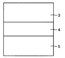
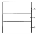
まず、図1の模式的断面図に示すように、たとえば、Si(シリコン)、SiC(炭化ケイ素)またはサファイア等からなる基板5上に、たとえばAlN(窒化アルミニウム)またはGaN等からなるバッファ層4を形成する。そして、バッファ層4上にGaN層3を形成する(第1工程)。
(Embodiment 1)
First, as shown in the schematic cross-sectional view of FIG. 1, a
ここで、GaN層3は、たとえば、原料としてトリメチルガリウムおよびアンモニアを用いたMOCVD(Metal Organic Chemical Vapor Deposition)法等によってGaN結晶をエピタキシャル成長させることにより形成することができる。
Here, the
次に、図2の模式的断面図に示すように、第1のAlGaN層1の厚さT1が1nm以上3nm以下となるように、GaN層3上に第1のAlGaN層1を形成する(第2工程)。これにより、GaN層3と第1のAlGaN層1との界面のGaN層3側に2次元電子ガス層2が形成される。
Next, as shown in the schematic cross-sectional view of FIG. 2, the
ここで、第1のAlGaN層1は、たとえば、トリメチルガリウム、トリメチルアルミニウムおよびアンモニアを含む原料を用いたMOCVD法等によってAlGaN結晶をエピタキシャル成長させることにより形成することができる。また、第1のAlGaN層1には、Si等のn型不純物等がドーピングされていてもよい。
Here, the
また、図2に示すように、第1のAlGaN層1の表面上には所定の形状にパターンニングされたフォトレジストマスク19を形成する。
Further, as shown in FIG. 2, a
ここで、フォトレジストマスク19は、後述するゲート電極が形成される領域(ゲート電極形成領域)に開口部19aを有し、開口部19aから第1のAlGaN層1の表面が露出するように形成される。
Here, the
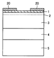
続いて、図3の模式的断面図に示すように、フォトレジストマスク19上から選択成長用マスク9を形成する。
Subsequently, as shown in the schematic cross-sectional view of FIG. 3, a
ここで、選択成長用マスク9としては、酸化シリコン膜および/または窒化シリコン膜を用いることが好ましい。選択成長用マスク9として酸化シリコン膜および/または窒化シリコン膜を用いた場合には、選択成長用マスク9をフッ酸またはフッ化アンモニウムで希釈したフッ酸等によって簡単にエッチングで除去することが可能となるため、後述する第2のAlGaN層の再成長による形成後に選択成長用マスク9をエッチングにより除去することが容易となる。
Here, as the
また、選択成長用マスク9は、たとえば、通常のCVD(Chemical Vapor Deposition)法またはスパッタ法により形成することができる。また、選択成長用マスク9の厚さは、たとえば50nm程度の厚さに形成することができるが、後述する第2のAlGaN層をリフトオフにより除去するためには、後述する第2のAlGaN層以上の厚さとすることが好ましい。
The
そして、図4の模式的断面図に示すように、フォトレジストマスク19を除去することにより、フォトレジストマスク19上に形成された選択成長用マスク9もリフトオフにより除去され、第1のAlGaN層1の表面のゲート電極形成領域のみに選択成長用マスク9が残される。
Then, as shown in the schematic cross-sectional view of FIG. 4, by removing the
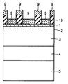
続いて、図5の模式的断面図に示すように、第1のAlGaN層1の表面のうち選択成長用マスク9で保護された領域(ゲート電極形成領域)以外の領域の少なくとも一部の表面上にAlGaNを再成長させて第2のAlGaN層20を形成する(第3工程)。
Subsequently, as shown in the schematic cross-sectional view of FIG. 5, at least a part of the surface of the surface of the
ここで、第2のAlGaN層20は、たとえば、トリメチルガリウム、トリメチルアルミニウムおよびアンモニアを含む原料を用いたMOCVD法、またはMBE(Molecular Beam Epitaxy)法等によってAlGaN結晶を再度エピタキシャル成長させることによって形成することができる。また、第2のAlGaN層20にも、Si等のn型不純物等がドーピングされていてもよい。
Here, the
また、第2のAlGaN層20の厚さT2は10nm以上であることが好ましく、13nm以上であることがより好ましい。第2のAlGaN層20が10nm以上の厚さに形成された場合、特に13nm以上の厚さに形成された場合には、2次元電子ガス層2における2次元電子ガス濃度をリセスゲート型HFETの特性を発揮させるのに十分に高くすることができる傾向にある。
Further, the thickness T2 of the
その後、図6の模式的断面図に示すように、選択成長用マスク9を除去する。ここで、選択成長用マスク9の表面上にはAlGaN結晶が成長していないか、もしくはアモルファスのAlGaNが形成されているが、アモルファスのAlGaNが形成されている場合でもリフトオフ等によって簡単に除去することができる。
Thereafter, as shown in the schematic sectional view of FIG. 6, the
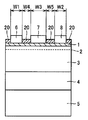
そして、図7の模式的断面図に示すように、第1のAlGaN層1の表面のゲート電極形成領域にゲート電極7を形成するとともに、第1のAlGaN層1の表面のゲート電極形成領域の両側に形成された第2のAlGaN層20の表面上にソース電極6およびドレイン電極8を形成する(第4工程)。
Then, as shown in the schematic sectional view of FIG. 7, the
ここで、ゲート電極7としては、たとえば、厚さ60nmのタングステン(W)膜、厚さ10nmの窒化タングステン(WN)膜および厚さ200nmの金(Au)膜を順次積層したもの等を用いることができる。
Here, as the
また、ソース電極6およびドレイン電極8としては、たとえば、厚さ2.5nmのハフニウム(Hf)膜、厚さ60nmのアルミニウム(Al)膜、厚さ10nmのハフニウム(Hf)膜、厚さ60nmの金(Au)膜および厚さ5000nmのタングステン(W)膜を順次積層したもの等を用いることができる。
As the
また、ソース電極6の幅W1はたとえば5μmとすることができ、ゲート電極7の幅W3はたとえば1.5μmとすることができ、ドレイン電極8の幅W2はたとえば5μmとすることができる。
The width W1 of the
また、ソース電極6とゲート電極7との間の距離W4はたとえば1.5μmとすることができ、ゲート電極7とドレイン電極8との間の距離W5はたとえば5μmとすることができる。
The distance W4 between the
以上の工程を含む方法によって、本発明においては、リセスゲート型HFETを製造することができる。 In the present invention, a recessed gate type HFET can be manufactured by the method including the above steps.
上述したように、本発明においては、第2工程においてGaN層3上に第1のAlGaN層1を1nm以上3nm以下の厚さにAlGaN結晶をエピタキシャル成長させることにより形成している(図2参照)。
As described above, in the present invention, in the second step, the
したがって、本発明においては、ドライエッチングを用いてリセスゲート構造を形成しているのではなく、第1のAlGaN層1および第2のAlGaN層20をそれぞれエピタキシャル成長させることによってリセスゲート構造を形成している。
Therefore, in the present invention, the recess gate structure is not formed by using dry etching, but the
ここで、AlGaN結晶のエピタキシャル成長速度は1nm/min程度とドライエッチング速度(1nm/s程度)に比べて遅いため、AlGaN結晶の成長の制御性が良く、面内バラツキ(目標とするエピタキシャル成長量の1%程度)もドライエッチングを用いた場合(目標とするエッチング量の10%程度)と比べて大幅に低減することができる。 Here, since the epitaxial growth rate of the AlGaN crystal is about 1 nm / min, which is slower than the dry etching rate (about 1 nm / s), the controllability of the growth of the AlGaN crystal is good, and in-plane variation (1 of the target epitaxial growth amount) %) Can be significantly reduced as compared with the case of using dry etching (about 10% of the target etching amount).
図15に、本発明によって製造されたリセスゲート型HFETの第1のAlGaN層1の厚さ(nm)と閾値電圧(V)との関係を示す。図15に示すように、本発明によって製造されたリセスゲート型HFETの第1のAlGaN層1の厚さが1nm以上3nm以下の範囲に制御された場合には、本発明によって製造されたリセスゲート型HFETはノーマリオフ特性を有することになる。
FIG. 15 shows the relationship between the thickness (nm) of the
本発明においては、第1のAlGaN層1はエピタキシャル成長により形成されることから、その面内バラツキを目標とするエピタキシャル成長量の1%程度とすることができる。したがって、本発明においては、たとえば第1のAlGaN層1のエピタキシャル成長量を2nmとすることによって、面内バラツキを考慮しても第1のAlGaN層1の厚さを2nm±0.02nmの範囲に制御することができるため、本発明によって製造されたリセスゲート型HFETは安定してノーマリオフ特性(ゲート電圧Vg=0V時にソース・ドレイン間の電流が0となる)を示すことになる。
In the present invention, since the
また、本発明においては、第1のAlGaN層1の厚さの面内バラツキを低減できることにより、ソース・ドレイン間に電流を流すためのゲート電圧(閾値電圧)のバラツキも低減することができる。
In the present invention, since the in-plane variation in the thickness of the
(実施の形態2)
まず、図8の模式的断面図に示すように、基板5上に、バッファ層4を形成する。そして、バッファ層4上にGaN層3を形成する(第1工程)。
(Embodiment 2)
First, as shown in the schematic sectional view of FIG. 8, the
次に、図9の模式的断面図に示すように、第1のAlGaN層1の厚さT1が1nm以上3nm以下となるように、GaN層3上に第1のAlGaN層1を形成する(第2工程)。
Next, as shown in the schematic cross-sectional view of FIG. 9, the
次いで、図10の模式的断面図に示すように、第1のAlGaN層1の表面上には所定の形状にパターンニングされたフォトレジストマスク19を形成する。
Next, as shown in the schematic cross-sectional view of FIG. 10, a
ここで、フォトレジストマスク19は、後述するソース電極、ゲート電極およびドレイン電極のそれぞれの形成領域に開口部19aをそれぞれ有しており、それぞれの開口部19aから第1のAlGaN層1の表面が露出するように形成される。
Here, the
そして、図11の模式的断面図に示すように、フォトレジストマスク19上から酸化シリコン膜および/または窒化シリコン膜からなる選択成長用マスク9をたとえば50nm程度の厚さにたとえばCVD法により形成する。
Then, as shown in the schematic cross-sectional view of FIG. 11, a
その後、フォトレジストマスク19を除去することにより、フォトレジストマスク19上に形成された選択成長用マスク9もリフトオフにより除去され、第1のAlGaN層1の表面のゲート電極形成領域のみに選択成長用マスク9が残される。
Thereafter, by removing the
続いて、図12の模式的断面図に示すように、第1のAlGaN層1の表面のうち選択成長用マスク9で保護された領域以外の領域の少なくとも一部の表面上にAlGaNを再成長させて第2のAlGaN層20を形成する(第3工程)。
Subsequently, as shown in the schematic cross-sectional view of FIG. 12, AlGaN is regrown on at least a part of the surface of the
そして、図13の模式的断面図に示すように、選択成長用マスク9を除去する。ここで、選択成長用マスク9の表面上にはAlGaN結晶が成長していないか、もしくはアモルファスのAlGaNが形成されているが、アモルファスのAlGaNが形成されている場合でもリフトオフ等によって簡単に除去することができる。
Then, as shown in the schematic sectional view of FIG. 13, the
その後、図14の模式的断面図に示すように、第1のAlGaN層1の表面の選択成長用マスク9の除去部分(第2のAlGaN層20が形成されていない部分)に、ソース電極6、ゲート電極7およびドレイン電極8をそれぞれ形成する(第4工程)。
Thereafter, as shown in the schematic cross-sectional view of FIG. 14, the
以上の工程を含む方法によって、本発明においては、リセスゲート型HFETを製造することができる。 In the present invention, a recessed gate type HFET can be manufactured by the method including the above steps.
本発明の実施の形態2によって製造されたリセスゲート型HFETにおいては、実施の形態1で説明した効果に加えて、ソース電極6およびドレイン電極7の直下のAlGaN層の厚さを実施の形態1で作製されたリセスゲート型HFETよりも薄くすることができるために、実施の形態1で作製されたリセスゲート型HFETよりもオン抵抗を低減することができる。
In the recessed gate type HFET manufactured according to the second embodiment of the present invention, in addition to the effects described in the first embodiment, the thickness of the AlGaN layer immediately below the
これは、本発明の実施の形態2によって製造されたリセスゲート型HFETにおいては、実施の形態1の場合と比べて、ソース電極6およびドレイン電極7のそれぞれと2次元電子ガス層2との距離を短くすることができるためと考えられる。
This is because the distance between the
また、AlGaN層全体(第1のAlGaN層1と第2のAlGaN層20)の厚さを薄くした場合には、2次元電子ガス層2における2次元電子ガス濃度が低くなる傾向にあるため、ソース電極6およびドレイン電極7のそれぞれの直下のAlGaN層のみの厚さを低減することが好ましい。
In addition, when the thickness of the entire AlGaN layer (the
なお、実施の形態2におけるその他の説明は、実施の形態1と同様である。
今回開示された実施の形態はすべての点で例示であって制限的なものではないと考えられるべきである。本発明の範囲は上記した説明ではなくて特許請求の範囲によって示され、特許請求の範囲と均等の意味および範囲内でのすべての変更が含まれることが意図される。
Other explanations in the second embodiment are the same as those in the first embodiment.
The embodiment disclosed this time should be considered as illustrative in all points and not restrictive. The scope of the present invention is defined by the terms of the claims, rather than the description above, and is intended to include any modifications within the scope and meaning equivalent to the terms of the claims.
本発明のリセスゲート型HFETの製造方法によれば、安定してノーマリオフ特性を有するリセスゲート型HFETを製造することができる。 According to the method for manufacturing a recessed gate type HFET of the present invention, a recessed gate type HFET having normally-off characteristics can be manufactured stably.
したがって、本発明により製造されたリセスゲート型HFETは、安定してノーマリオフ特性を有することから、パワー半導体装置等に好適に適用することができる。 Therefore, the recessed gate type HFET manufactured according to the present invention stably has normally-off characteristics and can be suitably applied to a power semiconductor device or the like.
1 第1のAlGaN層、2 2次元電子ガス層、3 GaN層、4 バッファ層、5 基板、6 ソース電極、7 ゲート電極、8 ドレイン電極、9 選択成長用マスク、10 サファイア基板、11 低温GaNバッファ層、12 アンドープGaN層、13 n型AlGaN層、14 n+型AlGaN層、19 フォトレジストマスク、19a 開口部、20 第2のAlGaN層。
DESCRIPTION OF
Claims (4)
基板上に窒化ガリウム層を形成する第1工程と、
前記窒化ガリウム層上に第1の窒化アルミニウムガリウム層を1nm以上3nm以下の厚さに形成する第2工程と、
前記第1の窒化アルミニウムガリウム層の表面のうちゲート電極形成領域以外の領域の少なくとも一部の表面上に第2の窒化アルミニウムガリウム層を再成長により形成する第3工程と、
前記第1の窒化アルミニウムガリウム層の表面のゲート電極形成領域にゲート電極を形成する第4工程と、
を含む、リセスゲート型HFETの製造方法。 A method of manufacturing a recessed gate type HFET having a heterojunction between a gallium nitride layer and an aluminum gallium nitride layer on a substrate, and a gate electrode formed on the aluminum gallium nitride layer,
A first step of forming a gallium nitride layer on the substrate;
A second step of forming a first aluminum gallium nitride layer on the gallium nitride layer to a thickness of 1 nm to 3 nm;
A third step of re-growing a second aluminum gallium nitride layer on at least a part of the surface of the first aluminum gallium nitride layer other than the gate electrode formation region;
A fourth step of forming a gate electrode in a gate electrode formation region on the surface of the first aluminum gallium nitride layer;
A method of manufacturing a recessed gate type HFET.
基板上に窒化ガリウム層を形成する第1工程と、
前記窒化ガリウム層上に第1の窒化アルミニウムガリウム層を1nm以上3nm以下の厚さに形成する第2工程と、
前記第1の窒化アルミニウムガリウム層の表面のうち、ソース電極、ドレイン電極およびゲート電極のそれぞれの形成領域以外の領域の少なくとも一部の表面上に第2の窒化アルミニウムガリウム層を再成長により形成する第3工程と、
前記第1の窒化アルミニウムガリウム層の表面上にソース電極、ドレイン電極およびゲート電極をそれぞれ形成する第4工程と、
を含む、リセスゲート型HFETの製造方法。 This is a method for manufacturing a recessed gate type HFET having a heterojunction portion of a gallium nitride layer and an aluminum gallium nitride layer on a substrate and having a source electrode, a drain electrode and a gate electrode formed on the aluminum gallium nitride layer, respectively. And
A first step of forming a gallium nitride layer on the substrate;
A second step of forming a first aluminum gallium nitride layer on the gallium nitride layer to a thickness of 1 nm to 3 nm;
A second aluminum gallium nitride layer is formed by regrowth on at least a part of the surface of the first aluminum gallium nitride layer other than the formation region of each of the source electrode, the drain electrode, and the gate electrode. A third step;
A fourth step of forming a source electrode, a drain electrode and a gate electrode on the surface of the first aluminum gallium nitride layer,
A method of manufacturing a recessed gate type HFET.
Priority Applications (1)
| Application Number | Priority Date | Filing Date | Title |
|---|---|---|---|
| JP2007068867A JP2008235347A (en) | 2007-03-16 | 2007-03-16 | Manufacturing process of recess gate type hfet |
Applications Claiming Priority (1)
| Application Number | Priority Date | Filing Date | Title |
|---|---|---|---|
| JP2007068867A JP2008235347A (en) | 2007-03-16 | 2007-03-16 | Manufacturing process of recess gate type hfet |
Publications (2)
| Publication Number | Publication Date |
|---|---|
| JP2008235347A true JP2008235347A (en) | 2008-10-02 |
| JP2008235347A5 JP2008235347A5 (en) | 2010-04-15 |
Family
ID=39907851
Family Applications (1)
| Application Number | Title | Priority Date | Filing Date |
|---|---|---|---|
| JP2007068867A Pending JP2008235347A (en) | 2007-03-16 | 2007-03-16 | Manufacturing process of recess gate type hfet |
Country Status (1)
| Country | Link |
|---|---|
| JP (1) | JP2008235347A (en) |
Cited By (7)
| Publication number | Priority date | Publication date | Assignee | Title |
|---|---|---|---|---|
| JP2010199481A (en) * | 2009-02-27 | 2010-09-09 | Sanken Electric Co Ltd | Field-effect semiconductor device and method of manufacturing the same |
| JP2013077635A (en) * | 2011-09-29 | 2013-04-25 | Sumitomo Electric Ind Ltd | Semiconductor device and manufacturing method of the same |
| US9685549B2 (en) | 2011-07-12 | 2017-06-20 | Panasonic Intellectual Property Management Co., Ltd. | Nitride semiconductor device and method for manufacturing same |
| WO2018154647A1 (en) * | 2017-02-22 | 2018-08-30 | 三菱電機株式会社 | High frequency amplifier |
| US10395932B2 (en) | 2016-12-19 | 2019-08-27 | Kabushiki Kaisha Toshiba | Semiconductor device and method for manufacturing the same |
| CN112640124A (en) * | 2018-06-27 | 2021-04-09 | 李湛明 | Gallium nitride device, gate drive circuit of integrated circuit and voltage regulator |
| JP7470008B2 (en) | 2020-10-19 | 2024-04-17 | 株式会社東芝 | Semiconductor Device |
Citations (6)
| Publication number | Priority date | Publication date | Assignee | Title |
|---|---|---|---|---|
| JPH09232336A (en) * | 1996-02-27 | 1997-09-05 | Fujitsu Ltd | Semiconductor device |
| JP2006100455A (en) * | 2004-09-29 | 2006-04-13 | New Japan Radio Co Ltd | Nitride semiconductor device and its manufacturing method |
| JP2006190991A (en) * | 2004-12-09 | 2006-07-20 | Matsushita Electric Ind Co Ltd | Field effect transistor and its manufacturing method |
| JP2006222160A (en) * | 2005-02-08 | 2006-08-24 | Nec Corp | Field effect transistor and its manufacturing method |
| JP2006261642A (en) * | 2005-02-17 | 2006-09-28 | Matsushita Electric Ind Co Ltd | Field effect transistor and method of fabricating the same |
| JP2006351762A (en) * | 2005-06-15 | 2006-12-28 | Matsushita Electric Ind Co Ltd | Semiconductor device and its manufacturing method |
-
2007
- 2007-03-16 JP JP2007068867A patent/JP2008235347A/en active Pending
Patent Citations (6)
| Publication number | Priority date | Publication date | Assignee | Title |
|---|---|---|---|---|
| JPH09232336A (en) * | 1996-02-27 | 1997-09-05 | Fujitsu Ltd | Semiconductor device |
| JP2006100455A (en) * | 2004-09-29 | 2006-04-13 | New Japan Radio Co Ltd | Nitride semiconductor device and its manufacturing method |
| JP2006190991A (en) * | 2004-12-09 | 2006-07-20 | Matsushita Electric Ind Co Ltd | Field effect transistor and its manufacturing method |
| JP2006222160A (en) * | 2005-02-08 | 2006-08-24 | Nec Corp | Field effect transistor and its manufacturing method |
| JP2006261642A (en) * | 2005-02-17 | 2006-09-28 | Matsushita Electric Ind Co Ltd | Field effect transistor and method of fabricating the same |
| JP2006351762A (en) * | 2005-06-15 | 2006-12-28 | Matsushita Electric Ind Co Ltd | Semiconductor device and its manufacturing method |
Cited By (11)
| Publication number | Priority date | Publication date | Assignee | Title |
|---|---|---|---|---|
| JP2010199481A (en) * | 2009-02-27 | 2010-09-09 | Sanken Electric Co Ltd | Field-effect semiconductor device and method of manufacturing the same |
| US9685549B2 (en) | 2011-07-12 | 2017-06-20 | Panasonic Intellectual Property Management Co., Ltd. | Nitride semiconductor device and method for manufacturing same |
| JP2013077635A (en) * | 2011-09-29 | 2013-04-25 | Sumitomo Electric Ind Ltd | Semiconductor device and manufacturing method of the same |
| US10395932B2 (en) | 2016-12-19 | 2019-08-27 | Kabushiki Kaisha Toshiba | Semiconductor device and method for manufacturing the same |
| WO2018154647A1 (en) * | 2017-02-22 | 2018-08-30 | 三菱電機株式会社 | High frequency amplifier |
| GB2572711A (en) * | 2017-02-22 | 2019-10-09 | Mitsubishi Electric Corp | High frequency amplifier |
| JPWO2018154647A1 (en) * | 2017-02-22 | 2019-11-07 | 三菱電機株式会社 | High frequency amplifier |
| US11025205B2 (en) | 2017-02-22 | 2021-06-01 | Mitsubishi Electric Corporation | High frequency amplifier |
| CN112640124A (en) * | 2018-06-27 | 2021-04-09 | 李湛明 | Gallium nitride device, gate drive circuit of integrated circuit and voltage regulator |
| CN112640124B (en) * | 2018-06-27 | 2024-02-20 | 苏州量芯微半导体有限公司 | Gate driving circuit of gallium nitride device and integrated circuit and voltage regulator |
| JP7470008B2 (en) | 2020-10-19 | 2024-04-17 | 株式会社東芝 | Semiconductor Device |
Similar Documents
| Publication | Publication Date | Title |
|---|---|---|
| US9171946B2 (en) | Nitride semiconductor device and method of manufacturing the same | |
| JP5032965B2 (en) | Nitride semiconductor transistor and manufacturing method thereof | |
| US20200152779A1 (en) | Normally-off hemt transistor with selective generation of 2deg channel, and manufacturing method thereof | |
| TWI429076B (en) | Binary group iii-nitride based high electron mobility transistors and methods of fabricating same | |
| US10026834B2 (en) | Method of manufacturing enhanced device and enhanced device | |
| JP5653607B2 (en) | GaN-based field effect transistor and manufacturing method thereof | |
| US20120061729A1 (en) | Nitride semiconductor device and method for fabricating the same | |
| JP4786730B2 (en) | Field effect transistor and manufacturing method thereof | |
| JP2006279032A (en) | Semiconductor device and manufacturing method thereof | |
| JP2007220895A (en) | Nitride semiconductor device and its manufacturing method | |
| JP2007324263A (en) | Field-effect transistor and manufacturing method thereof | |
| JP2006286942A (en) | Semiconductor device and method of manufacturing the same | |
| JP2008227501A (en) | Cap layer including aluminum nitride for nitride-based transistor, and method of fabricating the same | |
| JP2009182107A (en) | Semiconductor device | |
| JP2006190991A (en) | Field effect transistor and its manufacturing method | |
| JP2011082415A (en) | Group iii nitride-based field effect transistor and method of manufacturing the same | |
| JP2008235347A (en) | Manufacturing process of recess gate type hfet | |
| JP4474292B2 (en) | Semiconductor device | |
| JP2013077635A (en) | Semiconductor device and manufacturing method of the same | |
| JP5546104B2 (en) | GaN-based field effect transistor | |
| JP2005235935A (en) | High electron mobility transistor | |
| JP6064483B2 (en) | Compound semiconductor device and manufacturing method thereof | |
| JP2006286698A (en) | Electronic device and power converter | |
| JP2011129607A (en) | Gan-based mos field-effect transistor | |
| JP2009076673A (en) | Field-effect transistor using group iii nitride semiconductor |
Legal Events
| Date | Code | Title | Description |
|---|---|---|---|
| A521 | Written amendment |
Free format text: JAPANESE INTERMEDIATE CODE: A523 Effective date: 20100226 |
|
| A621 | Written request for application examination |
Free format text: JAPANESE INTERMEDIATE CODE: A621 Effective date: 20100226 |
|
| A977 | Report on retrieval |
Free format text: JAPANESE INTERMEDIATE CODE: A971007 Effective date: 20121029 |
|
| A131 | Notification of reasons for refusal |
Free format text: JAPANESE INTERMEDIATE CODE: A131 Effective date: 20121106 |
|
| A02 | Decision of refusal |
Free format text: JAPANESE INTERMEDIATE CODE: A02 Effective date: 20130305 |