JP2008203448A - Liquid crystal display device - Google Patents
Liquid crystal display device Download PDFInfo
- Publication number
- JP2008203448A JP2008203448A JP2007038287A JP2007038287A JP2008203448A JP 2008203448 A JP2008203448 A JP 2008203448A JP 2007038287 A JP2007038287 A JP 2007038287A JP 2007038287 A JP2007038287 A JP 2007038287A JP 2008203448 A JP2008203448 A JP 2008203448A
- Authority
- JP
- Japan
- Prior art keywords
- liquid crystal
- circuit board
- display device
- crystal display
- substrate
- Prior art date
- Legal status (The legal status is an assumption and is not a legal conclusion. Google has not performed a legal analysis and makes no representation as to the accuracy of the status listed.)
- Withdrawn
Links
Images


Classifications
-
- G—PHYSICS
- G02—OPTICS
- G02F—OPTICAL DEVICES OR ARRANGEMENTS FOR THE CONTROL OF LIGHT BY MODIFICATION OF THE OPTICAL PROPERTIES OF THE MEDIA OF THE ELEMENTS INVOLVED THEREIN; NON-LINEAR OPTICS; FREQUENCY-CHANGING OF LIGHT; OPTICAL LOGIC ELEMENTS; OPTICAL ANALOGUE/DIGITAL CONVERTERS
- G02F1/00—Devices or arrangements for the control of the intensity, colour, phase, polarisation or direction of light arriving from an independent light source, e.g. switching, gating or modulating; Non-linear optics
- G02F1/01—Devices or arrangements for the control of the intensity, colour, phase, polarisation or direction of light arriving from an independent light source, e.g. switching, gating or modulating; Non-linear optics for the control of the intensity, phase, polarisation or colour
- G02F1/13—Devices or arrangements for the control of the intensity, colour, phase, polarisation or direction of light arriving from an independent light source, e.g. switching, gating or modulating; Non-linear optics for the control of the intensity, phase, polarisation or colour based on liquid crystals, e.g. single liquid crystal display cells
- G02F1/133—Constructional arrangements; Operation of liquid crystal cells; Circuit arrangements
- G02F1/1333—Constructional arrangements; Manufacturing methods
- G02F1/1345—Conductors connecting electrodes to cell terminals
- G02F1/13452—Conductors connecting driver circuitry and terminals of panels
Abstract
Description
本発明は、横電界液晶表示装置に関し、特に、静電気の影響による表示ムラを防止した横電界表示装置に関する。 The present invention relates to a horizontal electric field liquid crystal display device, and more particularly to a horizontal electric field display device that prevents display unevenness due to the influence of static electricity.
横電界方式で液晶を制御する液晶表示装置は、電界を液晶パネル面に対して平行方向に印加して、液晶分子を液晶パネル面内で旋回させたときの液晶セルの光透過率の変化を利用して表示を行っているため、大きな角度視野から観察しても鮮明な映像としてみることができ、視野角に対する依存性がほとんどないという特徴を有している(例えば、特許文献1を参照)。 A liquid crystal display device that controls liquid crystal using the horizontal electric field method applies changes in the light transmittance of the liquid crystal cell when an electric field is applied in a direction parallel to the liquid crystal panel surface and the liquid crystal molecules are rotated in the liquid crystal panel surface. Since the display is performed by using the display, it can be seen as a clear image even when observed from a large angle field of view, and has a feature that there is almost no dependency on the field of view (see, for example, Patent Document 1). ).
しかしながら、視野角拡大という特性を有する反面、外部から与えられた静電気が液晶セル内に蓄積されやすく、チャージアップが発生しやすいという欠点がある。以下に詳細について述べる。横電界方式の場合、TFT基板側に櫛歯状に設けたソース電極とコモン電極間の電界のみにより液晶を制御しているため、対向側のCF(カラーフィルター)基板の断面にはITO等の電極は存在しない。 However, although it has the characteristic of widening the viewing angle, there is a drawback that static electricity applied from the outside is easily accumulated in the liquid crystal cell and charge-up is likely to occur. Details are described below. In the case of the lateral electric field method, since the liquid crystal is controlled only by the electric field between the source electrode and the common electrode provided in a comb-teeth shape on the TFT substrate side, the cross section of the CF (color filter) substrate on the opposite side is made of ITO or the like. There are no electrodes.
従って、CF側偏光板の表面を手で触れた場合、その静電気はCF側偏光板を通してCFガラス基板まで達し、TFT基板とCF基板間に電位差が生じる。この電位差に反応して液晶セル中に封入された液晶分子が誤動作しチャージアップが発生する。このチャージアップを解決するために採られていた従来の構成を図9〜12に示す。図9は従来の液晶表示装置の構成を模式的に示す平面図である。TFTが形成された基板2と対向基板1の間には液晶層が封入され、対向基板1の表面には透明導電膜4が製膜され、その上に偏光板3が設けられている。基板2の端子部には液晶ドライバIC5が実装され、モールド樹脂6が設けられている。また、この端子部には回路基板7が接続され、対向基板上の透明導電膜4を導電テープ8により回路基板に接地している(例えば、特許文献2を参照)。図10に図9の点線c−c’での断面を示す。図示するように、導電テープ8は回路基板7上のGND端子電極11に接着されている。また、回路基板7の裏面にはチップ部品10が実装されている。さらに、図11に示すように偏光板3の表面に透明導電膜としてITO膜26をスパッタリング法により成膜する方法や(例えば、特許文献3を参照)、図12に示すように透明導電膜シート27を偏光板3の上に貼合せる方法(例えば、特許文献4を参照)が知られている。いずれの方式も、透明導電膜4は導電部材や筐体を介して回路基板7のGND電極端子11と接続(接地)されており、静電気が逃げるような構造になっている。
近年表示装置の小型化のために、有効表示エリア以外は極小化が求められており、液晶パネル上の透明導電膜と導電部材の接続に供与できる面積は小さくなっている。また、薄型化のために、回路基板にはフレキシブル回路基板が使用され、筐体のない表示装置も増えてきている。そのため、液晶パネル上の透明導電膜は、導電材として銅箔に導電接着剤を塗布した導電テープを用い、その導電テープを介してFPCのGNDに接続する方法がとられるようになって来た。しかし、フレキシブル回路基板に貼り付けた導電テープは、フレキシブル故にはがれやすく、特にフレキシブル回路基板を折り曲げて使う場合には安定した接続が困難である。さらには、液晶ドライバICを液晶パネル上にCOG実装する方式が主流になっており、図10に示すように、導電テープ8は液晶パネルと回路基板7間を、COG実装のモールド樹脂6の上を通って接続される。一般的にモールド樹脂としてはシリコン系が使用されるため、導電テープの接着性は悪く、接続安定性を一層低下させている。そこで、本発明の目的は、上記従来技術の欠点を解決し、小型、薄型の表示装置においても、横電界方式液晶表示装置のチャージアップを完全に防いだ液晶表示装置を提供するものである。
In recent years, miniaturization of displays other than the effective display area has been required for miniaturization of display devices, and the area that can be provided for connection between the transparent conductive film on the liquid crystal panel and the conductive member has been reduced. In addition, in order to reduce the thickness, a flexible circuit board is used as a circuit board, and a display device without a housing is increasing. For this reason, the transparent conductive film on the liquid crystal panel uses a conductive tape obtained by applying a conductive adhesive to copper foil as a conductive material, and a method of connecting to the GND of the FPC via the conductive tape has come to be adopted. . However, the conductive tape affixed to the flexible circuit board is easy to peel off because it is flexible, and stable connection is difficult particularly when the flexible circuit board is bent and used. Furthermore, the method of COG mounting the liquid crystal driver IC on the liquid crystal panel has become the mainstream, and as shown in FIG. 10, the
本発明は上記した目的を達成するため、基本的には、以下に記載されたような技術構成を採用するものである。即ち、本発明に係わる液晶表示装置の第1態様は、液晶パネルの透明基板の液晶と反対側に透明導電膜が形成され、この透明導電膜が導電テープを介して回路基板に接地された横電界方式の液晶表示装置において、前記導電テープが前記回路基板を挟んだ構造になっていることを特徴とするものであり、又、第二態様は、液晶パネルの透明基板の液晶と反対側に透明導電膜が形成され、この透明導電膜が導電テープを介して回路基板に接地された横電界方式の液晶表示装置において、前記導電テープの幅が液晶パネル側より前記回路基板側が広くなっており、回路基板上で折り返すことにより、回路基板を挟む構造にしたことを特徴とするものであり、又、第三態様は、液晶パネルの透明基板の液晶と反対側に透明導電膜が形成され、この透明導電膜が導電テープを介して回路基板に接地された横電界方式の液晶表示装置において、前記導電テープが、回路基板上で折り返した裏面側で前記回路基板に接地されていることを特徴とするものである。 In order to achieve the above-described object, the present invention basically employs a technical configuration as described below. That is, in the first aspect of the liquid crystal display device according to the present invention, a transparent conductive film is formed on the opposite side of the transparent substrate of the liquid crystal panel, and the transparent conductive film is grounded to the circuit board via a conductive tape. The electric field type liquid crystal display device is characterized in that the conductive tape has a structure sandwiching the circuit board, and the second mode is on the opposite side of the liquid crystal of the transparent substrate of the liquid crystal panel. In a horizontal electric field type liquid crystal display device in which a transparent conductive film is formed and this transparent conductive film is grounded to a circuit board via a conductive tape, the width of the conductive tape is wider on the circuit board side than on the liquid crystal panel side. The circuit board is sandwiched by folding on the circuit board, and the third aspect has a transparent conductive film formed on the opposite side of the liquid crystal of the transparent substrate of the liquid crystal panel, This transparent In a horizontal electric field type liquid crystal display device in which a conductive film is grounded to a circuit board via a conductive tape, the conductive tape is grounded to the circuit board on a back surface side folded on the circuit board. Is.
本発明の液晶表示装置では、導電テープが回路基板を挟み込む構造であるため、導電テープが回路基板から剥がれなくなり、液晶パネル上の透明導電膜を、導電テープを介して確実に接地することができる。その結果液晶パネル表面に生じた静電気は速やかにGNDに逃げるため、横電界液晶表示装置においてチャージアップによる表示不良を防止することができ、表示品質の良好な液晶表示装置を提供することが可能になる。 In the liquid crystal display device of the present invention, since the conductive tape sandwiches the circuit board, the conductive tape does not peel off from the circuit board, and the transparent conductive film on the liquid crystal panel can be reliably grounded via the conductive tape. . As a result, the static electricity generated on the surface of the liquid crystal panel quickly escapes to GND, so that it is possible to prevent display defects due to charge-up in the horizontal electric field liquid crystal display device, and to provide a liquid crystal display device with good display quality. Become.
本発明の表示装置は、薄膜トランジスタが形成された基板と、この基板と対向して液晶を挟持する対向基板と、液晶を基板と平行な方向の電界で駆動するために基板上に形成された電極を備える横電界液晶パネルと、横電界液晶パネルに隣接して配置された回路基板を備えている表示装置であって、対向基板の液晶と反対側の面に形成された透明導電膜と透明導電膜を回路基板に接地するための導電テープを有するとともに、導電テープが回路基板を挟むように折り曲げられ、導電テープは透明導電膜と回路基板の表面と裏面に接着された構造である。 The display device of the present invention includes a substrate on which a thin film transistor is formed, a counter substrate that holds the liquid crystal opposite to the substrate, and an electrode formed on the substrate for driving the liquid crystal with an electric field in a direction parallel to the substrate. And a circuit board disposed adjacent to the horizontal electric field liquid crystal panel, the transparent conductive film and the transparent conductive film formed on the opposite surface of the counter substrate to the liquid crystal The conductive tape has a conductive tape for grounding the film to the circuit board, and the conductive tape is bent so as to sandwich the circuit board, and the conductive tape is bonded to the transparent conductive film and the front and back surfaces of the circuit board.
さらに、導電テープは、透明導電膜と回路基板の表面に接着される部位では折り曲げられない構造で、回路基板の表面と回路基板の裏面に接着される部位では折り曲げられた構造である。さらに、導電テープの幅が液晶パネル側より回路基板側が広くなっており、回路基板上で折り返すことにより、回路基板を挟む構造になっている。あるいは、導電テープを略L字状の外形に形成することとした。 Further, the conductive tape has a structure that is not bent at a portion that is bonded to the surface of the transparent conductive film and the circuit board, and is bent at a portion that is bonded to the front surface of the circuit board and the back surface of the circuit board. Further, the width of the conductive tape is wider on the circuit board side than on the liquid crystal panel side, and the circuit board is sandwiched by folding back on the circuit board. Alternatively, the conductive tape is formed in a substantially L-shaped outer shape.
また、上述のいずれかの構成で、導電テープは、折り返した裏面側で回路基板に接地されていることとした。また、回路基板がフレキシブル回路基板とした。また、液晶ドライバICは基板上の端子部にCOG実装され、端子部にモールド樹脂が設けられた構成とした。さらに、モールド樹脂をシリコン樹脂とした。 In any of the above-described configurations, the conductive tape is grounded to the circuit board on the folded back side. The circuit board was a flexible circuit board. Further, the liquid crystal driver IC was configured to be COG-mounted on the terminal portion on the substrate and provided with a mold resin on the terminal portion. Further, the mold resin was a silicon resin.
以下に本発明の実施例について図面を用いて説明する。 Embodiments of the present invention will be described below with reference to the drawings.
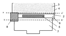
本実施例の液晶表示装置の構成を図1乃至図3、および図7、図8に模式的に示す。図1は本発明の液晶表示装置の平面図、図2は図1の液晶表示装置をa−a'の位置で切断したときのパネル部の断面図、図3は図1の液晶表示装置をb−b'の位置で切断したときの液晶表示装置の回路基板部の断面図、図7は本発明に用いた液晶表示パネルの断面模式図、図8は本発明に用いた液晶表示パネルの能動素子画素部の詳細図、図13は本発明の液晶表示装置の偏光板の断面構造を示す詳細図である。はじめに、図7および図8にもとづいて、スイッチング素子としてのTFTが形成された基板2について説明する。透明ガラス製の基板2上には、ドレインバスライン22とゲートバスライン21が縦横に形成され、ドレインバスライン22はスイッチング素子15を介してソース電極25と接続されている。コモン電極24とソース電極23は互いに対向した櫛歯状の形状をしており、これら2つの電極間にかかる電界により液晶の配向状態が制御される。これらの電極を被覆するように保護絶縁膜16が形成され、その上に配向膜17が形成されている。
The configuration of the liquid crystal display device of this embodiment is schematically shown in FIGS. 1 to 3, 7 and 8. FIG. 1 is a plan view of the liquid crystal display device of the present invention, FIG. 2 is a cross-sectional view of the panel section when the liquid crystal display device of FIG. 1 is cut at the position aa ′, and FIG. 3 is the liquid crystal display device of FIG. 7 is a cross-sectional view of the circuit board portion of the liquid crystal display device when cut at the position bb ′, FIG. 7 is a schematic cross-sectional view of the liquid crystal display panel used in the present invention, and FIG. FIG. 13 is a detailed view showing the cross-sectional structure of the polarizing plate of the liquid crystal display device of the present invention. First, the
次に、カラーフィルターが形成された対向基板1について説明する。透明ガラス製の対向基板1上には、ブラックマトリクス13がマトリクス状に形成され、それらの間を覆う様にR(赤)、G(緑)、B(青)の着色層12がストライプ状に形成されている。これらの着色層12を保護するために透明の保護膜14が形成され、その上に配向隙17が形成されている。基板2と対向基板1の間には、正の誘電率異方性を有する液晶19が扶持されており、配向膜17を介して液晶19は2つの基板1,2にほぼ平行になるように配向している。また、セル厚を制御するために対向基板1にはポストスペーサ18が形成されており、表示部外の周辺シール剤20には棒状スペーサが添加されている。対向基板1の液晶19と接する側と反対側には透明導電膜4が形成されており、基板2と対向基板1のそれぞれの最外側には一対の偏光板3が貼り付けられている。一対の偏光板3は透過軸が互いに直交するように、いわゆるクロスニコル配置されている。一方の偏光板の透過軸は液晶分子19の配向方向と一致するように配置され、他方の偏光板の透過軸は一方の偏光板の透過軸と直交するように配置されている。
Next, the
次に、本発明の液晶表示装置の特徴である、チャージアップを防止するための導電テープ部の構造について、図1乃至図3を用いて説明する。基板2の端子部には液晶ドライバIC5がCOG実装されており、その周囲には耐久性向上のためにモールド剤6が塗布されている。フレキシブル回路基板7には一方の面に配線パターン9および抵抗、コンデンサなど液晶パネルの駆動に必要なチップ部品10が実装されており、他方の面にはGND端子電極11が設けられている。対向基板1上の透明導電膜4は、導電テープ8を介してフレキシブル回路基板7上のGND端子電極11に接地されており、チャージアップを防止するようになっている。図2および図3に示すように、導電テープ8は液晶表示パネルおよびフレキシブル回路基板7をはさむように折り曲げて貼り付けてある。導電テープとしては金属箔に導電粘着剤を塗布したものを使用することができ、例えば、住友スリーエム(株)製のAl箔導電性テープ1170やCu箔に導電性粘着剤を塗布した製品名1181などを使うことができる。
Next, the structure of the conductive tape portion for preventing charge-up, which is a feature of the liquid crystal display device of the present invention, will be described with reference to FIGS. A liquid
本実施例の構造にすることにより、導電テープが回路基板から剥がれなくなり、液晶パネル上の透明導電膜4を、導電テープを介して確実に接地することができた。その結果液晶パネル表面に生じた静電気は速やかにGNDに逃げるため、横電界液晶表示装置においてチャージアップによる表示不良を防止することができ、表示品質の良好な液晶表示装置を提供することが可能になった。
With the structure of this example, the conductive tape was not peeled off from the circuit board, and the transparent
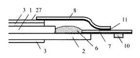
本実施例の液晶表示装置の構成を図4および図5に模式的に示す。図4は本発明の液晶表示装置の平面図、図5は図4の液晶表示装置をb−b’の位置で切断したときの液晶表示装置の回路基板部の断面図を示す。本実施例では、導電テープ8を図4に示すように導電テープの幅を液晶パネル側より回路基板側が広い形状にし、図5に示すようにフレキシブル回路基板7部でのみ導電テープ8を折り返す構成にした。
The structure of the liquid crystal display device of this example is schematically shown in FIGS. 4 is a plan view of the liquid crystal display device of the present invention, and FIG. 5 is a cross-sectional view of the circuit board portion of the liquid crystal display device when the liquid crystal display device of FIG. 4 is cut at the position b-b ′. In this embodiment, the
本実施例の構成では、導電テープ8が液晶パネルより外にはみ出すこがとなく、よりコンパクトな液晶表示装置を得ることができた。
In the configuration of this example, the
本実施例の液晶表示装置の構成を図6に示す。本実施例は、実施例2の構成において、図6に示すようにフレキシブル回路基板7上のGND端子電極11を配線パターン9と同一面に形成し、導電テープ8を折り返した裏面側で接地する構成にした。本実施例の構成では、フレキシブル回路基板の配線パターン9およびGND端子電極11が同一面に形成することができ、フレキシブル回路基板の製造コストを低減することが可能になった。
The configuration of the liquid crystal display device of this example is shown in FIG. In the present embodiment, in the configuration of the second embodiment, as shown in FIG. 6, the
導電テープを介して確実に接地した液晶表示装置を提供することが可能になるので、高耐久性が要求される携帯情報機器の表示装置に適応できる。 Since it is possible to provide a liquid crystal display device that is securely grounded via a conductive tape, it can be applied to a display device of a portable information device that requires high durability.
1 対向基板
2 基板
3 偏光板
4 透明導電膜
5 液晶ドライバIC
6 モールド剤
7 フレキシブル回路基板
8 導電部材
9 配線パターン
10 チップ部品
11 GND端子電極
12 カラーフィルター
13 ブラックマトリックス
14 保護膜
15 スイッチング素子
16 保護絶縁膜
17 配向膜
18 ポストスペーサ
19 液晶
20 シール剤
21 ゲートバスライン
22 ドレインバスライン
23 ソース電極
24 コモン電極
25 ソース電極
26 透明導電膜
27 透明導電膜シート
1
6
Claims (8)
前記横電界液晶パネルに隣接して配置された回路基板と、
前記対向基板の前記液晶と反対側の面に形成された透明導電膜と、
前記透明導電膜を前記回路基板に接地するための導電テープを有するとともに、
前記導電テープが前記回路基板を挟むように折り曲げられ、前記導電テープは前記透明導電膜と前記回路基板の表面と裏面に接着された構造であることを特徴とする液晶表示装置。 A substrate on which a thin film transistor is formed; a counter substrate that faces the substrate and sandwiches liquid crystal between the substrate; and the liquid crystal is formed on the substrate to drive the liquid crystal with an electric field in a direction parallel to the substrate. A lateral electric field liquid crystal panel comprising electrodes;
A circuit board disposed adjacent to the lateral electric field liquid crystal panel;
A transparent conductive film formed on a surface of the counter substrate opposite to the liquid crystal;
While having a conductive tape for grounding the transparent conductive film to the circuit board,
The liquid crystal display device, wherein the conductive tape is bent so as to sandwich the circuit board, and the conductive tape is bonded to the transparent conductive film and the front and back surfaces of the circuit board.
Priority Applications (1)
| Application Number | Priority Date | Filing Date | Title |
|---|---|---|---|
| JP2007038287A JP2008203448A (en) | 2007-02-19 | 2007-02-19 | Liquid crystal display device |
Applications Claiming Priority (1)
| Application Number | Priority Date | Filing Date | Title |
|---|---|---|---|
| JP2007038287A JP2008203448A (en) | 2007-02-19 | 2007-02-19 | Liquid crystal display device |
Publications (2)
| Publication Number | Publication Date |
|---|---|
| JP2008203448A true JP2008203448A (en) | 2008-09-04 |
| JP2008203448A5 JP2008203448A5 (en) | 2010-01-14 |
Family
ID=39781039
Family Applications (1)
| Application Number | Title | Priority Date | Filing Date |
|---|---|---|---|
| JP2007038287A Withdrawn JP2008203448A (en) | 2007-02-19 | 2007-02-19 | Liquid crystal display device |
Country Status (1)
| Country | Link |
|---|---|
| JP (1) | JP2008203448A (en) |
Cited By (6)
| Publication number | Priority date | Publication date | Assignee | Title |
|---|---|---|---|---|
| JP2010164946A (en) * | 2008-12-19 | 2010-07-29 | Toshiba Mobile Display Co Ltd | Image display device |
| JP2011002608A (en) * | 2009-06-18 | 2011-01-06 | Sony Corp | In-plane switching mode liquid crystal display device |
| US8711305B2 (en) | 2011-04-07 | 2014-04-29 | Mitsubishi Electric Corporation | Liquid crystal display apparatus |
| CN105114876A (en) * | 2015-09-21 | 2015-12-02 | 京东方科技集团股份有限公司 | Backlight module and display device |
| US9823527B2 (en) | 2014-02-27 | 2017-11-21 | Mitsubishi Electric Corporation | Liquid crystal display |
| CN107408361A (en) * | 2015-03-10 | 2017-11-28 | 夏普株式会社 | Display device |
Citations (4)
| Publication number | Priority date | Publication date | Assignee | Title |
|---|---|---|---|---|
| JPH08185714A (en) * | 1994-12-29 | 1996-07-16 | Nitto Denko Corp | Conductive adhesive tape |
| JPH11149085A (en) * | 1995-10-12 | 1999-06-02 | Hitachi Ltd | Liquid crystal display device |
| JP2001147441A (en) * | 1999-11-19 | 2001-05-29 | Nec Corp | Transverse electric field liquid crystal display device |
| JP2004063535A (en) * | 2002-07-25 | 2004-02-26 | Nippon Tekku Kk | Method of etching substrate |
-
2007
- 2007-02-19 JP JP2007038287A patent/JP2008203448A/en not_active Withdrawn
Patent Citations (4)
| Publication number | Priority date | Publication date | Assignee | Title |
|---|---|---|---|---|
| JPH08185714A (en) * | 1994-12-29 | 1996-07-16 | Nitto Denko Corp | Conductive adhesive tape |
| JPH11149085A (en) * | 1995-10-12 | 1999-06-02 | Hitachi Ltd | Liquid crystal display device |
| JP2001147441A (en) * | 1999-11-19 | 2001-05-29 | Nec Corp | Transverse electric field liquid crystal display device |
| JP2004063535A (en) * | 2002-07-25 | 2004-02-26 | Nippon Tekku Kk | Method of etching substrate |
Cited By (8)
| Publication number | Priority date | Publication date | Assignee | Title |
|---|---|---|---|---|
| JP2010164946A (en) * | 2008-12-19 | 2010-07-29 | Toshiba Mobile Display Co Ltd | Image display device |
| JP2011002608A (en) * | 2009-06-18 | 2011-01-06 | Sony Corp | In-plane switching mode liquid crystal display device |
| US8711305B2 (en) | 2011-04-07 | 2014-04-29 | Mitsubishi Electric Corporation | Liquid crystal display apparatus |
| US9823527B2 (en) | 2014-02-27 | 2017-11-21 | Mitsubishi Electric Corporation | Liquid crystal display |
| CN107408361A (en) * | 2015-03-10 | 2017-11-28 | 夏普株式会社 | Display device |
| CN105114876A (en) * | 2015-09-21 | 2015-12-02 | 京东方科技集团股份有限公司 | Backlight module and display device |
| WO2017049882A1 (en) * | 2015-09-21 | 2017-03-30 | 京东方科技集团股份有限公司 | Backlight module and display device |
| US10139557B2 (en) | 2015-09-21 | 2018-11-27 | Boe Technology Group Co., Ltd. | Display device with backlight module using electrically conductive adhesive and grounding wire |
Similar Documents
| Publication | Publication Date | Title |
|---|---|---|
| JP3025257B1 (en) | Display panel | |
| US8547505B2 (en) | Liquid crystal display | |
| JP4386862B2 (en) | Liquid crystal display device and manufacturing method thereof | |
| US9995981B2 (en) | Liquid crystal display device | |
| US9618817B2 (en) | Array substrate and narrow bezel-type liquid crystal display device including the same | |
| US9285637B2 (en) | Liquid-crystal display | |
| US9176338B2 (en) | Liquid crystal display panel and method for manufacturing the same | |
| TW201814464A (en) | Display device | |
| JP5448940B2 (en) | Liquid crystal display | |
| JP2011170200A (en) | Liquid crystal device and method of manufacturing liquid crystal device | |
| KR20100005883A (en) | Array substrate and liquid crystal display apparatus having the same | |
| WO2010058495A1 (en) | Touch panel and display device using the same | |
| KR101901253B1 (en) | Display Device integrating with Touch Screen and Method for Manufacturing the Same | |
| JP2015084017A (en) | Liquid crystal display device | |
| US10353253B2 (en) | Mounting substrate and display device | |
| JP2014157311A (en) | Display device and manufacturing method of display device | |
| US20090033857A1 (en) | Liquid crystal display device | |
| JP2008203448A (en) | Liquid crystal display device | |
| US7742140B2 (en) | In-plane switching mode liquid crystal display device with common voltage transmission wire | |
| WO2017022609A1 (en) | Display panel | |
| CN106873213B (en) | Liquid crystal display panel and method of manufacturing the same | |
| JP2008197218A (en) | Liquid crystal display device | |
| JP6395541B2 (en) | Liquid crystal panel, liquid crystal display device including the same, and method for manufacturing liquid crystal panel | |
| KR101989001B1 (en) | Display device | |
| US20150160510A1 (en) | Liquid crystal display device |
Legal Events
| Date | Code | Title | Description |
|---|---|---|---|
| RD01 | Notification of change of attorney |
Free format text: JAPANESE INTERMEDIATE CODE: A7421 Effective date: 20091105 |
|
| RD01 | Notification of change of attorney |
Effective date: 20091113 Free format text: JAPANESE INTERMEDIATE CODE: A7421 |
|
| RD01 | Notification of change of attorney |
Free format text: JAPANESE INTERMEDIATE CODE: A7421 Effective date: 20091117 |
|
| A521 | Written amendment |
Free format text: JAPANESE INTERMEDIATE CODE: A523 Effective date: 20091118 |
|
| A621 | Written request for application examination |
Effective date: 20091118 Free format text: JAPANESE INTERMEDIATE CODE: A621 |
|
| A131 | Notification of reasons for refusal |
Free format text: JAPANESE INTERMEDIATE CODE: A131 Effective date: 20111213 |
|
| A977 | Report on retrieval |
Free format text: JAPANESE INTERMEDIATE CODE: A971007 Effective date: 20111214 |
|
| A761 | Written withdrawal of application |
Effective date: 20120206 Free format text: JAPANESE INTERMEDIATE CODE: A761 |