JP2008202995A - Specific detecting method of substance to be inspected using photocurrent, pad used therein, sensor unit, and measuring instrument - Google Patents
Specific detecting method of substance to be inspected using photocurrent, pad used therein, sensor unit, and measuring instrument Download PDFInfo
- Publication number
- JP2008202995A JP2008202995A JP2007037181A JP2007037181A JP2008202995A JP 2008202995 A JP2008202995 A JP 2008202995A JP 2007037181 A JP2007037181 A JP 2007037181A JP 2007037181 A JP2007037181 A JP 2007037181A JP 2008202995 A JP2008202995 A JP 2008202995A
- Authority
- JP
- Japan
- Prior art keywords
- pad
- electrode
- substance
- working electrode
- sensitizing dye
- Prior art date
- Legal status (The legal status is an assumption and is not a legal conclusion. Google has not performed a legal analysis and makes no representation as to the accuracy of the status listed.)
- Pending
Links
Images


Abstract
Description
本発明は、光電流を用いて、核酸、外因性内分泌撹乱物質、抗原等の特異的結合性を有する被検物質を特異的に検出する方法、それに用いられるパッド、センサユニット、および測定装置に関する。 The present invention relates to a method for specifically detecting a test substance having specific binding properties such as a nucleic acid, an exogenous endocrine disrupting substance, and an antigen using a photocurrent, a pad used in the method, a sensor unit, and a measuring apparatus. .
近年、人の疾病の病症および進度に対する予測を可能にするホルモン、タンパク質を簡便で安価に検出できる検査システムの考案が試みられている。また、ダイオキシンを始めとする外因性内分泌撹乱物質(環境ホルモン)の生殖系及び神経系等への障害が社会問題化しており、その検出方法が望まれている。 In recent years, attempts have been made to devise a test system that can easily and inexpensively detect hormones and proteins that enable prediction of the disease state and progress of human diseases. In addition, disorders of the reproductive system and nervous system of exogenous endocrine disrupting substances (environmental hormones) such as dioxins have become a social problem, and a method for detecting such problems is desired.
また、増感色素を用いてか光から電気エネルギーを発生させる太陽電池の原理を利用して、増感色素の光励起により生じる光電流を、披検物質(DNA、蛋白などの生体分子)の検出に利用する提案がなされている(特許文献1、特許文献2、特許文献3)。さらに、免疫クロマト法の原理を利用し、ホルモン、蛋白質、酵素等のような分析物質を電気化学的に検出する方法が行われている(特許文献4、特許文献5、特許文献6)。
In addition, using the principle of solar cells that generate electrical energy from light using sensitizing dyes, photocurrents generated by photoexcitation of sensitizing dyes are used to detect test substances (biomolecules such as DNA and proteins). (
上述したように光電流を用いて被検物質(DNA、蛋白などの生体分子)を特異的に検出する際、これまでは電解液を満たしたセンサユニットを用いて行われていた。しかしこの場合センサユニットの液漏れ、センサユニット内への送液に時間がかかる、構成が複雑である送液機構を検出装置に保持させる必要がある、送液機構を保持することにより検出装置が大型となるなどの問題があった。また、簡便に検出でき、装置構成を簡単にする目的で、行われてきた免疫クロマト法の原理を利用し、ホルモン、蛋白質、酵素等のような分析物質を電気化学的に検出する方法は、標識検出物の分離を吸収パッドにより行う必要があり、装置構造の複雑化、被検物質の点着から検出まで時間がかかるといった問題があった。 As described above, when a test substance (biomolecules such as DNA and protein) is specifically detected using a photocurrent, it has so far been performed using a sensor unit filled with an electrolytic solution. However, in this case, the sensor unit leaks liquid, it takes time to feed liquid into the sensor unit, and it is necessary to hold the liquid feeding mechanism having a complicated structure in the detection device. There was a problem of becoming large. In addition, for the purpose of simplifying detection and simplifying the apparatus configuration, a method for electrochemically detecting an analyte such as a hormone, protein, enzyme, etc., using the principle of immunochromatography that has been performed, There is a problem that the labeled detection object needs to be separated by an absorption pad, and the structure of the apparatus is complicated, and it takes time from spotting a test substance to detection.
本発明者らは、今般、被検物質を特異的に反応させるための媒体及び電解質媒体としての役割を持つ吸水性のパッドを用いて、増感色素の光励起により生じる光電流を用いた被検物質の特異的検出を行った。この検出法を用いることで、電解液の代わりに電解質含有パッドを使用することができ、装置構造および検出手順を大幅に簡素化することができた。また従来のイムノクロマト法では必要であった標識検出物の分離に必要な吸収パッドを必要としない構造のパッドを使用することができ、装置構造の簡素化および被検物質の点着から検出までの時間短縮ができるとの知見を得た。さらに、本技術を用いて光電流を検出した場合、特異的に結合していない標識検出物由来の光電流はほとんど検出されず、精度良い検出を行うことができるとの知見も得た。 The present inventors have recently used a water-absorbing pad having a role as a medium for specifically reacting a test substance and an electrolyte medium, and a test using a photocurrent generated by photoexcitation of a sensitizing dye. Specific detection of the substance was performed. By using this detection method, an electrolyte-containing pad could be used instead of the electrolyte solution, and the device structure and detection procedure could be greatly simplified. In addition, it is possible to use a pad with a structure that does not require an absorption pad that is necessary for separation of a labeled detection object, which was necessary in the conventional immunochromatography method. The knowledge that time can be shortened was acquired. Furthermore, when a photocurrent was detected using this technology, a photocurrent derived from a labeled detection substance that was not specifically bound was hardly detected, and it was found that accurate detection can be performed.
したがって、本発明は、増感色素の光励起により生じる光電流を用いた被検物質の特異的検出において、装置構造および検出手順を大幅に簡素化することを目的としている。 Therefore, an object of the present invention is to greatly simplify the device structure and detection procedure in specific detection of a test substance using a photocurrent generated by photoexcitation of a sensitizing dye.
すなわち、本発明による、光電流を用いた被検物質の特異的検出方法は、
被検物質が直接または間接的に特異的に結合したプローブ物質を表面に備え、かつ該結合により増感色素が固定されてなる作用電極と、対電極とを上記パッドに接触した状態で、電解質存在下、前記作用電極に光を照射して前記増感色素を光励起させ、該光励起された増感色素から前記作用電極への電子移動に起因して前記作用電極と前記対電極との間に流れる光電流を検出することを含んでなる。ここで、特異的結合は、被検物質が直接または間接的に結合可能なプローブ物質を表面に備えた作用電極を前記パッドに接触させた後、被検物質および溶媒を少なくとも含有してなる試料液を前記パッドに含浸させて行われる。また、前記増感色素および電解質は、それぞれ試料液またはパッドのいずれかに含有される。
That is, the specific detection method of a test substance using photocurrent according to the present invention is as follows:
In the state in which a probe substance to which a test substance is directly or indirectly specifically bound is provided on the surface and a sensitizing dye is fixed by the binding and a counter electrode are in contact with the pad, the electrolyte In the presence, the working electrode is irradiated with light to photoexcite the sensitizing dye, and between the working electrode and the counter electrode due to electron transfer from the photoexcited sensitizing dye to the working electrode. Detecting a flowing photocurrent. Here, specific binding refers to a sample containing at least a test substance and a solvent after contacting a working electrode having a probe substance on its surface with which the test substance can bind directly or indirectly. It is carried out by impregnating the pad with a liquid. The sensitizing dye and the electrolyte are contained in either the sample solution or the pad, respectively.
また、本発明のパッドは、電解質の存在下、増感色素の光励起により生じる光電流を用いた被検物質の特異的検出に用いられるパッドであって、
吸水性物質を含んでなり、被検物質、増感色素および電解質の媒体としての役割を有するパッドである。
The pad of the present invention is a pad used for specific detection of a test substance using a photocurrent generated by photoexcitation of a sensitizing dye in the presence of an electrolyte,
A pad comprising a water-absorbing substance and serving as a medium for a test substance, a sensitizing dye and an electrolyte.
本発明のパッドは、単一又は複数用いても良い。また、本発明のパッドには、増感色素および/または電解質をさらに含んでもよい。 A single pad or a plurality of pads of the present invention may be used. The pad of the present invention may further contain a sensitizing dye and / or an electrolyte.
さらに、本発明による、増感色素の光励起により生じる光電流を用いた被検物質の特異的検出に用いられるセンサユニットは、
作用電極と、
前記電極と対向して設けられる対電極と、
前記作用電極および前記対電極の間に挟持される、上記パッドと
を備えてなり、前記作用電極および前記対電極の各電極表面が前記パッドと接触してなるものである。
Furthermore, according to the present invention, a sensor unit used for specific detection of a test substance using a photocurrent generated by photoexcitation of a sensitizing dye,
A working electrode;
A counter electrode provided opposite to the electrode;
The pad is sandwiched between the working electrode and the counter electrode, and each electrode surface of the working electrode and the counter electrode is in contact with the pad.
また、本発明の他の態様によるセンサユニットは、
作用電極および対電極がパターニングされてなる電極ユニットと、
前記作用電極および前記対電極の各電極表面に接触して設けられる上記パッドと
を備えてなり、前記作用電極および前記対電極の各電極表面が前記パッドと接触してなるものである。
In addition, a sensor unit according to another aspect of the present invention includes:
An electrode unit in which a working electrode and a counter electrode are patterned;
A pad provided in contact with each electrode surface of the working electrode and the counter electrode, and each electrode surface of the working electrode and the counter electrode is in contact with the pad.
さらに、本発明による、増感色素の光励起により生じる光電流を用いた被検物質の特異的検出に用いられる測定装置は、
上記センサユニットと、
前記作用電極に光を照射するための光源と、
前記作用電極と前記対電極との間を流れる電流を測定する電流計と
を備えたものである。
Furthermore, the measuring apparatus used for specific detection of a test substance using a photocurrent generated by photoexcitation of a sensitizing dye according to the present invention,
The sensor unit;
A light source for irradiating the working electrode with light;
And an ammeter for measuring a current flowing between the working electrode and the counter electrode.
本発明によれば、増感色素の光励起により生じる光電流を用いた被検物質の特異的検出において、本発明のパッドを用いることで装置構造および検出手順を大幅に簡素化することができ、また、試料液の点着から検出までの時間短縮を達成することができ、さらに、被検物質の検出を精度よく行うことができる。 According to the present invention, in the specific detection of a test substance using a photocurrent generated by photoexcitation of a sensitizing dye, the structure of the apparatus and the detection procedure can be greatly simplified by using the pad of the present invention, Further, it is possible to shorten the time from the spotting of the sample solution to the detection, and furthermore, it is possible to detect the test substance with high accuracy.
パッド
本発明に用いるパッドは、増感色素の光励起により生じる光電流を用いた被検物質の特異的検出において電解液の代わりに電解質含有パッドを使用することができる。さらに、本発明のパッドは、被検物質、増感色素および電解質の媒体として用いられる。被検物質を含む試料液をパッドに含浸させることで、被検物質とプローブ物質との特異的な結合をパッド上で行うことができる。このパッドには、電解質および増感色素を含んでも良い。また、被検物質の特異的検出において複数のパッドを用いることで、それぞれに異なる物質を含ませておくことができる。例えば、パッドを二枚用いる場合は、一方に電解質を、他方に増感色素を含ませておき、これらのパッドを重ね合わせた状態で検出に供することができる。
Pad As the pad used in the present invention, an electrolyte-containing pad can be used in place of the electrolytic solution in specific detection of a test substance using a photocurrent generated by photoexcitation of a sensitizing dye. Furthermore, the pad of the present invention is used as a medium for a test substance, a sensitizing dye and an electrolyte. By impregnating the sample solution containing the test substance into the pad, specific binding between the test substance and the probe substance can be performed on the pad. The pad may contain an electrolyte and a sensitizing dye. Further, by using a plurality of pads in the specific detection of the test substance, different substances can be included in each. For example, when two pads are used, an electrolyte can be included in one and a sensitizing dye can be included in the other, and these pads can be used for detection.
本発明において電解質は、パッド中を自由に移動して増感色素、作用電極、および対電極との間で電子の授受に関与できるものであれば限定されず、幅広い種類の電解質が使用可能である。好ましい電解質は、光照射により励起された色素に電子を供与するための還元剤(電子供与剤)として機能できる物質であり、そのような物質の例としては、ヨウ化ナトリウム(NaI)、ヨウ化カリウム(KI)、ヨウ化カルシウム(CaI2)、ヨウ化リチウム(LiI)、ヨウ化アンモニウム(NH4I)、テトラプロピルアンモニウムヨージド(NPr4I)、チオ硫酸ナトリウム(Na2S2O3)、亜硫酸ナトリウム(Na2SO3)、ヒドロキノン、K4[Fe(CN)6]・3H2O、フェロセン−1,1´−ジカルボン酸、フェロセンカルボン酸、水素化ホウ素ナトリウム(NaBH4)、トリエチルアミン、チオシアネートアンモニウム、ヒドラジン(N2H4)、アセトアルデヒド(CH3CHO)、N,N,N´,N´−テトラメチル−p−フェニレンジアミン二塩酸塩(TMPD)、L−アスコルビン酸、亜テルル酸ナトリウム(Na2TeO3)、塩化鉄(II)四水和物(FeCl2・4H2O)、EDTA、システイン、トリエタノールアミン、トリプロピルアミン、ヨウ素を含むヨウ化リチウム(I/LiI)、トリス(2-クロロエチル)リン酸塩(TCEP)、ジチオスレイトール(DTT)、2−メルカプトエタノール、2−メルカプトエタノールアミン、二酸化チオ尿素、(COOH)2、HCHO、およびこれらの組合せが挙げられ、より好ましくは、NaI、KI、CaI2、LiI、NH4I、テトラプロピルアンモニウムヨージド(NPr4I)、チオ硫酸ナトリウム(Na2S2O3)、および亜硫酸ナトリウム(Na2SO3)、およびこれらの混合物であり、さらに好ましくは、テトラプロピルアンモニウムヨージド(NPr4I)である。
In the present invention, the electrolyte is not limited as long as it can freely move in the pad and participate in the exchange of electrons with the sensitizing dye, the working electrode, and the counter electrode, and a wide variety of electrolytes can be used. is there. A preferable electrolyte is a substance that can function as a reducing agent (electron donor) for donating an electron to a dye excited by light irradiation. Examples of such a substance include sodium iodide (NaI), iodide Potassium (KI), calcium iodide (CaI 2 ), lithium iodide (LiI), ammonium iodide (NH 4 I), tetrapropylammonium iodide (NPr 4 I), sodium thiosulfate (Na 2 S 2 O 3) ),
本発明の好ましい態様によれば、パッドは、20%以上の含水率を有するのが好ましく、より好ましくは30%以上であり、さらに好ましくは40%以上である。このような含水率であると、光電流を検出した際に高い光電流を検出することができ、検出感度が向上する。含水率は(1mm3 辺りの含水量)/(吸水性物質の密度)より求める。なお、ここで言う含水率は光電流を検出する際のパッドの含水率であって、保管時に上記含水率を満たしていなくてもよい。 According to a preferred embodiment of the present invention, the pad preferably has a moisture content of 20% or more, more preferably 30% or more, and further preferably 40% or more. When the moisture content is such, a high photocurrent can be detected when the photocurrent is detected, and the detection sensitivity is improved. The water content is obtained from (water content around 1 mm 3 ) / (density of water-absorbing substance). In addition, the moisture content said here is the moisture content of the pad at the time of detecting a photocurrent, Comprising: It does not need to satisfy | fill the said moisture content at the time of storage.
本発明のパッドの形態としては、作用電極および対電極との良好な密着性が確保されるように各電極との接触部分が平滑な平面とされているのが好ましい。したがって、作用電極と対電極との間に挟み込んで使用する場合には、密着性に影響しないように均一な厚みを有する形態とするのが好ましい。一方、作用電極および対電極が同一平面状にパターニングされてなる電極ユニットを使用する場合には、少なくとも電極ユニットと接触する片側面のみが平滑な平面とされていればよく、厚さや厚さの均一性は特段問題とならない。 As a form of the pad of this invention, it is preferable that the contact part with each electrode is made into a smooth plane so that favorable adhesiveness with a working electrode and a counter electrode is ensured. Therefore, when sandwiched between the working electrode and the counter electrode, it is preferable to have a uniform thickness so as not to affect the adhesion. On the other hand, when using an electrode unit in which the working electrode and the counter electrode are patterned in the same plane, it is sufficient that at least one side surface in contact with the electrode unit is a smooth plane. Uniformity is not a particular problem.
本発明の好ましい態様によれば、パッドは0.01〜10mmの厚さを有するのが好ましく、より好ましくは0.1〜3mmの厚さを有する。このような厚さであるとパッドを単独で取り扱うのに適した強度が得られやすいので、作用電極と対電極の間に容易に挟み込んだり、取り外したりでき、あるいは持ち運んだりすることができ、その結果、センサユニット構造および検出手順を大幅に簡素化できる。また、光電流測定に悪影響を与えることもない。 According to a preferred embodiment of the present invention, the pad preferably has a thickness of 0.01 to 10 mm, more preferably 0.1 to 3 mm. With such a thickness, it is easy to obtain a strength suitable for handling the pad alone, so it can be easily sandwiched, removed or carried between the working electrode and the counter electrode. As a result, the sensor unit structure and detection procedure can be greatly simplified. Moreover, it does not adversely affect the photocurrent measurement.
本発明においてパッドは吸水性物質を含んでなる。吸水性物質は、綿、麻、ウール、絹、セルロースなどの天然繊維;ろ紙、製紙などに用いられるパルプ繊維;レーヨンなどの再生繊維;ろ紙などに用いられるガラス繊維;フェルト、スポンジなどに用いられる合成繊維から選択される少なくとも一種の繊維を含んでなるのが好ましく、適度な強度、含水量、電極への密着性を示す吸水性物質であれば限定されない。なお、繊維の加工方法は特定の加工方法に限定されない。 In the present invention, the pad comprises a water-absorbing substance. Water-absorbing substances include natural fibers such as cotton, hemp, wool, silk, and cellulose; pulp fibers used for filter paper and papermaking; regenerated fibers such as rayon; glass fibers used for filter paper; felts and sponges, etc. It is preferable to contain at least one kind of fiber selected from synthetic fibers, and it is not limited as long as it is a water-absorbing substance exhibiting an appropriate strength, water content, and adhesion to an electrode. The fiber processing method is not limited to a specific processing method.
本発明の好ましい態様によれば、パッドはシート状である。好ましい例としては、ろ紙、メンブレンフィルター、ガラスフィルター、ろ布などが挙げられ、より好ましくはろ紙、メンブレンフィルターである。 According to a preferred aspect of the present invention, the pad is in the form of a sheet. Preferable examples include filter paper, membrane filter, glass filter, filter cloth and the like, and filter paper and membrane filter are more preferable.
光電流を用いた被検物質の特異的検出
前述の通り、本発明のパッドは増感色素の光励起により生じる光電流を用いた被検物質の特異的検出に用いられるものである。この増感色素の光励起により生じる光電流を用いた被検物質の特異的検出方法について、以下に具体的に説明する。
Specific Detection of Test Substance Using Photocurrent As described above, the pad of the present invention is used for specific detection of a test substance using a photocurrent generated by photoexcitation of a sensitizing dye. A specific detection method for a test substance using a photocurrent generated by photoexcitation of the sensitizing dye will be specifically described below.
本発明による、光電流を用いた被検物質の特異的検出方法は、
被検物質が直接または間接的に特異的に結合可能なプローブ物質を表面に備えた作用電極を上記パッドに接触させ、前記パッドに試料液を含浸させた後、プローブ物質との特異的結合により増感色素が固定されてなる前記作用電極に光を照射して前記増感色素を光励起させ、該光励起された増感色素から前記作用電極への電子移動に起因して前記作用電極と前記パッドに接触した対電極との間に流れる光電流を検出すること
を含んでなるものである。
The specific detection method of a test substance using photocurrent according to the present invention is as follows:
A working electrode having a probe substance that can be specifically bound directly or indirectly to the test substance is brought into contact with the pad, the sample liquid is impregnated into the pad, and then the probe is specifically bound to the probe substance. Irradiating light to the working electrode on which a sensitizing dye is fixed to photoexcite the sensitizing dye, and the working electrode and the pad are caused by electron transfer from the photoexcited sensitizing dye to the working electrode. And detecting a photocurrent flowing between the counter electrode and the counter electrode.
この方法にあっては、まず、被検物質および溶媒を少なくとも含む試料液と、作用電極とを用意する。ここで、溶媒は被検物質、増感色素、および電解質を溶解または分散可能な液体であって、水および/または水性溶媒であり、好ましくは水である。本発明に用いる作用電極は、被検物質と直接または間接的に特異的な結合が可能なプローブ物質を表面に備えた電極である。すなわち、プローブ物質は、被検物質と直接、特異的に結合する物質のみならず、被検物質を受容体蛋白質分子等の媒介物質に特異的に結合させて得られる結合体と特異的に結合可能な物質であってよい。次いで、増感色素の共存下、試料液を作用電極に接触させて、プローブ物質に被検物質を直接または間接的に特異的に結合させ、この結合により増感色素を作用電極に固定させる。増感色素は、光励起に応じて作用電極に電子を放出可能な物質であり、被検物質の特異的検出法がサンドイッチ法である場合、プローブ物質は1次抗体で、増感色素は2次抗体に標識されてなり、被検物質の特異的検出法がレセプター結合アッセイである場合、プローブ物質としてペプチド、タンパク質、DNAを用いて、増感色素はレセプタータンパク質に標識されてなり、被検物質の特異的検出法が競合法である場合、増感色素はプローブ物質に特異的に結合可能な第二の被検物質に標識される。
なお、増感色素で標識された物質および電解質は試料液またはパッドいずれに含まれてもよい。
In this method, first, a sample solution containing at least a test substance and a solvent and a working electrode are prepared. Here, the solvent is a liquid capable of dissolving or dispersing the test substance, the sensitizing dye, and the electrolyte, and is water and / or an aqueous solvent, preferably water. The working electrode used in the present invention is an electrode provided on the surface with a probe substance capable of specific binding directly or indirectly to a test substance. That is, the probe substance specifically binds not only to a substance that directly binds specifically to the test substance, but also to a conjugate obtained by specifically binding the test substance to a mediator such as a receptor protein molecule. It may be a possible substance. Next, in the presence of the sensitizing dye, the sample solution is brought into contact with the working electrode to specifically bind the test substance directly or indirectly to the probe substance, and the sensitizing dye is fixed to the working electrode by this binding. The sensitizing dye is a substance that can emit electrons to the working electrode in response to photoexcitation. When the specific detection method of the test substance is the sandwich method, the probe substance is the primary antibody and the sensitizing dye is the secondary antibody. When the antibody is labeled and the specific detection method of the test substance is a receptor binding assay, peptide, protein, or DNA is used as a probe substance, and the sensitizing dye is labeled with the receptor protein. When the specific detection method is a competitive method, the sensitizing dye is labeled with a second test substance that can specifically bind to the probe substance.
The substance labeled with the sensitizing dye and the electrolyte may be contained in either the sample solution or the pad.
そして、作用電極をパッドに接触させた後、作用電極に光を照射して増感色素を光励起させると、光励起された増感色素から電子受容物質へ電子移動が起こる。この電子移動に起因して作用電極と対電極との間に流れる光電流を検出することにより、被検物質を高い感度および精度で検出することができる。また、この検出電流は試料液中の被検試料濃度との高い相関関係を有しているので、測定された電流量または電気量に基づき被検試料の定量測定を行うことができる。 Then, after the working electrode is brought into contact with the pad, when the sensitizing dye is photoexcited by irradiating the working electrode with light, electron transfer from the photoexcited sensitizing dye to the electron accepting substance occurs. By detecting the photocurrent flowing between the working electrode and the counter electrode due to this electron movement, the test substance can be detected with high sensitivity and accuracy. Further, since the detected current has a high correlation with the test sample concentration in the sample solution, the test sample can be quantitatively measured based on the measured current amount or electric quantity.
センサユニットおよび測定装置
本発明のパッドを用いることにより、構造が大幅に簡素化された安価でかつ小型のセンサユニットないし測定装置を構築することができる。これは、本発明のパッドの使用により、作用電極と対電極との間に電解液を充填して行われる従来法において必要とされていた、電解液を送液する機構(例えばポンプ、バルブ、およびそれらの制御機構)、液漏れ防止機構(例えばパッキン)、および電解液の廃液処理といった複雑な機構ないし工程が不要となり、また被検物質の特異的な結合をパッド上で行うことにより、非常に簡素なリアクター機構となる。
Sensor Unit and Measuring Device By using the pad of the present invention, an inexpensive and small sensor unit or measuring device having a greatly simplified structure can be constructed. This is because the use of the pad of the present invention requires a mechanism (for example, a pump, a valve, And their control mechanism), liquid leakage prevention mechanism (for example, packing), and complicated mechanism or process such as waste liquid treatment of the electrolyte are not required, and the specific binding of the test substance is performed on the pad. It becomes a simple reactor mechanism.
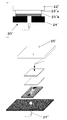
本発明の第一の態様によるセンサユニットは、作用電極と、作用電極と対向して設けられる対電極と作用電極との間に挟持されるパッドとを備えてなり、作用電極表面がパッドと接触してなるものである。本発明の第一の態様によるセンサユニットは、さらに対電極を備えても良く、この場合、パッドはさらに対電極と接触している。すなわち、作用電極の表側(被検物質が固定化されている側)と対電極の導電面(白金など)が対向し、パッドと接触する配置になっている。図1、図2に第一の態様によるセンサユニットの断面図および分解図を示す。図1に示されるセンサユニット10にあっては、作用電極11が対電極12の下方に位置し、作用電極11および対電極12の間にパッド13が挟持される。また、センサユニット10は、作用電極11を支持する押さえ部材14を備える。センサユニット10の最上部には、押さえ部材14に向かって、対電極12、パッド13、および作用電極11を互いに密着させるように下方に押さえる対向部材15が設けられる。本発明のセンサユニットにあっては、各部品が積み上げられる順序は図示例に限定されず、図1に示される順序と逆の順序で上下逆さとなるように積み上げられてもよく、この場合には、対電極を支持する対向部材と、対向部材に向けて、対電極、パッド、および作用電極を互いに密着させるように押さえる押さえ部材とがさらに設けられる構成とすればよい。また、図示例では各部材が水平に配置されているが、各部材を立てた状態で配置してもよい。押さえ部材14には、光励起のための光を通すための開口部または透光部をさらに備えてなるのが好ましい。図2に示されるセンサユニット10´には図1のセンサユニットおいて、吸水性物質により形成した2枚のパッド13´a、13´b、を用いた際のセンサユニットの断面図および分解図を示す。パッド以外の構成においては前述した図1の態様と同様の構成である。なお、作用電極の電流計と接続するための接点は、コンタクトプローブ16、コンタクトプローブ16´で行うのが好ましく、対電極においても同様である。
The sensor unit according to the first aspect of the present invention includes a working electrode, a counter electrode provided opposite to the working electrode, and a pad sandwiched between the working electrodes, and the surface of the working electrode is in contact with the pad. It is made. The sensor unit according to the first aspect of the present invention may further include a counter electrode, in which case the pad is further in contact with the counter electrode. That is, the front side of the working electrode (the side on which the test substance is immobilized) and the conductive surface (platinum or the like) of the counter electrode face each other and are in contact with the pad. 1 and 2 show a sectional view and an exploded view of the sensor unit according to the first embodiment. In the
本発明の第二の態様によるセンサユニットは、作用電極および対電極が同一平面上にパターニングされてなる電極ユニットと、作用電極および対電極の各電極表面に接触して設けられるパッドとを備えてなる。図3〜6に第二の態様によるセンサユニットの断面図および分解図を示す。図3に示されるセンサユニット20にあっては、電極ユニット21と対向して対向部材22が設けられ、電極ユニット21および対向部材22の間にパッド23が挟持される。また、センサユニット20は、電極ユニット21を支持する押さえ部材24を備える。すなわち、押さえ部材24上に被検物質を固定化した側が上になるように電極ユニット21が配置され、対向部材22は、押さえ部材24に向けて、電極ユニット21およびパッド23を互いに密着させるように押さえつける。図4に示されるセンサユニット20´には図3のセンサユニットおいて、吸水性物質により形成した2枚のパッド23´a、23´b、を用いた際のセンサユニットの断面図および分解図を示す。パッド以外の構成においては前述した図3の態様と同様の構成である。一方、図5に示されるセンサユニット30にあっては、電極ユニット31には電極ユニットを支持する対向部材34がさらに設けられ、押さえ部材32が、対向部材34に向けて、パッド33および電極ユニット31を互いに密着させるように押さえる。すなわち、対向部材34上に、被検物質を固定化した側が上になるように電極ユニット31が置かれ、電極ユニット31上にパッド33が配置される。図6に示されるセンサユニット30´には図5のセンサユニットおいて、吸水性物質により形成した2枚のパッド33´a、33´bを用いた際のセンサユニットの断面図および分解図を示す。本発明のセンサユニットにあっては、各部品が積み上げられる順序は図示例に限定されず、図3〜6に示される順序と逆の順序で上下逆さとなるように積み上げられてもよい。また、図示例では各部材が水平に配置されているが、各部材を立てた状態で配置してもよい。押さえ部材24,24´、32、32´は、光励起のための光を通すための1つ以上の開口部または透光部をさらに備えてなるのが好ましい。なお、図5、図6に示されるセンサユニット30、センサユニット30´では照射光がパッドを通過することになるので、着色性を有する電解質等を使用する場合には光強度の減衰が問題とならないように、光源や電解質濃度を適宜調整するのが好ましい。なお、作用電極及び対電極の電流計と接続するための接点は、コンタクトプローブ25、25´、35、35´で行うのが好ましく、対電極においても同様である。
A sensor unit according to a second aspect of the present invention includes an electrode unit in which a working electrode and a counter electrode are patterned on the same plane, and a pad provided in contact with each electrode surface of the working electrode and the counter electrode. Become. 3 to 6 show a sectional view and an exploded view of the sensor unit according to the second embodiment. In the
第一の態様および第二の態様のいずれにおいても、センサユニット10、10´、20、20´、30、30´には、作用電極に光を照射するための光源17、17´、27、27´、37、37´と、作用電極と対電極との間を流れる電流を測定する電流計(図示せず)とがさらに設けられ、測定装置として構築されることができる。電流計はnAレベルの検出可能なものが好ましい。このような構成において、光源からの光は作用電極の表面に照射される。なお、図1〜4に示されるセンサユニット10、10´、20、20´において、光源17、17´、27、27´からの光は作用電極11、11´、電極ユニット21、21´の裏側より照射され、透明な作用電極11、11´、電極ユニット21、21´を透過して作用電極11、11´、電極ユニット21、21´の表面に到達する。一方、図5および6に示されるセンサユニット30、30´にあっては、光源37,37´からの光は押さえ部材32、32´の開口部を通過して電極ユニット31、31´の表面に到達する。こうして作用電極に到達した光による増感色素の光励起により発生する光電流値は電流計で検出されることができる。作用電極および対極を電流計に接続する手段は限定されるものではなく、例えば、リード線を直接接続する、あるいは図示例のようにコンタクトプローブ16、16´、25、25´、35、35´を介して接続することなどの手段を採用することができる。特に、測定毎に着脱する作用電極については、コンタクトプローブを用いることで作用電極の着脱が容易になるという利点がある。
In any of the first aspect and the second aspect, the
本発明の別の好ましい態様によれば、複数のセンサユニットを組み合わせた測定装置を作製することも可能である。その場合、センサユニットには光源があらかじめ複数個設けられてなり、かつ、測定装置が、該複数個の光源を切り換えて照射する機構をさらに備えてなることができる。 According to another preferred aspect of the present invention, it is also possible to produce a measuring device in which a plurality of sensor units are combined. In that case, the sensor unit may be provided with a plurality of light sources in advance, and the measuring apparatus may further include a mechanism for switching and irradiating the plurality of light sources.
さらに本発明の好ましい態様によれば、複数のセンサユニットを組み合わせた測定装置にはXY移動機構(図示せず)が取り付けられ、光源およびセンサユニットをXY方向に相対的に移動させて、光源が作用電極上をXY方向に走査移動しながら照射できるように構成されるのが好ましい。これにより、複数のセンサユニット上の被検物質固定化スポットに光を照射することができる。特に、本発明のセンサユニットでは電解液の送液が不要なため構造が簡素化されたため、センサユニット自体のXY移動も容易に行うことができる。この場合、XY移動機構はコンピュータや装置に組み込まれるソフトウェアによって、移動速度、移動経路などを指定できるように構成されるのが好ましい。 Furthermore, according to a preferred aspect of the present invention, an XY moving mechanism (not shown) is attached to a measuring apparatus that combines a plurality of sensor units, and the light source and sensor unit are moved relative to each other in the XY direction so that the light source It is preferable that the irradiation can be performed while scanning the working electrode in the X and Y directions. Thereby, light can be irradiated to the test substance fixed spots on the plurality of sensor units. In particular, since the sensor unit of the present invention does not require the feeding of the electrolytic solution, the structure is simplified, and therefore the XY movement of the sensor unit itself can be easily performed. In this case, it is preferable that the XY moving mechanism is configured so that the moving speed, the moving route, and the like can be designated by software incorporated in the computer or apparatus.
本発明の好ましい態様によれば、光照射に伴い発生する電流値が電流計で測定され、その結果がコンピュータや装置内のメモリに送られて、順次データ保存できるようにされるのが好ましい。このようにしてメモリ内に保存された光電流値は、数値もしくはリアルタイム表示の経時変化グラフとしてディスプレイに表示させることができる。得られたデータより、光非照射時と光照射時の電流値を適切なデータポイントより読み取り、その差を用いて、試料中の物質濃度定量を行うことができる。また、これらのデータの読み取りから定量までをもソフトウェア上で自動処理させることもできる。 According to a preferred aspect of the present invention, it is preferable that a current value generated by light irradiation is measured by an ammeter, and the result is sent to a memory in a computer or apparatus so that data can be stored sequentially. The photocurrent value stored in the memory in this manner can be displayed on the display as a numerical value or a time-dependent graph of real time display. From the obtained data, the current value at the time of non-irradiation and at the time of light irradiation is read from an appropriate data point, and the concentration of the substance in the sample can be determined using the difference. In addition, it is possible to automatically process from reading to quantification of these data on software.
被検物質およびプローブ物質
本発明における被検物質としては、プローブ物質と特異的な結合性を有する物質であれば特に限定ない。本方法では、被検物質と直接または間接的に特異的に結合可能なプローブ物質を作用電極表面に担持させておくことにより、被検物質をプローブ物質に直接または間接的に特異的に結合させて検出することが可能となる。
Test substance and probe substance The test substance in the present invention is not particularly limited as long as it is a substance having specific binding properties with the probe substance. In this method, a probe substance capable of specifically binding directly or indirectly to the test substance is supported on the surface of the working electrode, so that the test substance is directly or indirectly specifically bound to the probe substance. Can be detected.
すなわち、本発明にあっては、被検物質およびプローブ物質として互いに特異的に結合可能なものを選択することができる。すなわち、本発明の好ましい態様によれば、特異的な結合性を有する物質を被検物質とし、被検物質と特異的に結合する物質をプローブ物質として作用電極に担持させるのが好ましい。これにより、作用電極上に被検物質を直接、特異的に結合させて検出することができる。被検物質を直接、特異的に結合させる態様の被検物質およびプローブ物質の組合せの好ましい例としては、抗原および抗体の組合せが挙げられる。一方で被検物質を間接的に特異的に結合可能にプローブ物質に結合させる態様の被検物質およびプローブ物質の組合せの好ましい例としては、以下に示すサンドイッチ法を採用した場合の例やレセプター結合アッセイを採用した場合の例があげられる。 That is, in the present invention, substances that can specifically bind to each other can be selected as the test substance and the probe substance. That is, according to a preferred embodiment of the present invention, it is preferable that a substance having specific binding properties be a test substance and a substance that specifically binds to the test substance be carried on the working electrode as a probe substance. As a result, the test substance can be directly bound and detected on the working electrode. A preferable example of the combination of the test substance and the probe substance in such a manner that the test substance is directly and specifically bound is a combination of an antigen and an antibody. On the other hand, preferred examples of the combination of the test substance and the probe substance in such a manner that the test substance is bound to the probe substance in such a manner that it can be specifically and indirectly bound to the probe substance include the case where the sandwich method shown below is adopted and receptor binding An example of employing an assay is given.
測定方法
本発明のパッドを用いた測定方法にあっては、先ず、被検物質が直接または間接的に特異的に結合するプローブ物質を作用電極表面に固定させる。
Measurement Method In the measurement method using the pad of the present invention, first, a probe substance to which a test substance specifically binds directly or indirectly is immobilized on the surface of the working electrode.
こうして被検物質と直接または間接的に特異的に結合するプローブ物質が固定化された作用電極をパッドに接触させ、被検物質を含む試料液を点着後、直接的若しくは間接的な特異的結合により増感色素が作用電極に固定される。 In this way, the working electrode on which the probe substance that specifically binds directly or indirectly to the test substance is immobilized is brought into contact with the pad, and the sample liquid containing the test substance is spotted and then directly or indirectly specific. The sensitizing dye is fixed to the working electrode by the binding.
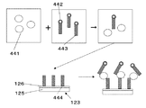
本発明の好ましい態様によれば、被検物質に抗原を用いて、免疫アッセイ、特にサンドイッチ法を採用した場合、以下のような態様をとり得る。1次抗体をプローブ物質とし、被検物質である抗原が1次抗体に特異的に結合後、増感色素で標識された2次抗体が前記抗原と特異的結合により作用電極に固定化される。この態様における被検物質である抗原および増感色素で標識された2次抗体のプローブ物質である1次抗体への固定化工程を図7に示す。図7に示されるように、増感色素40で標識された2次抗体41が、被検物質である抗原42存在下、抗体43に特異的に結合する。
According to a preferred aspect of the present invention, when an immunoassay, particularly a sandwich method, is employed using an antigen as a test substance, the following aspects can be taken. A primary antibody is used as a probe substance, and an antigen as a test substance is specifically bound to the primary antibody, and then a secondary antibody labeled with a sensitizing dye is immobilized on the working electrode by specific binding with the antigen. . FIG. 7 shows an immobilization process of the secondary antibody labeled with the antigen as the test substance and the sensitizing dye to the primary antibody as the probe substance in this embodiment. As shown in FIG. 7, the
本発明の好ましい態様によれば、被検物質に抗原を用いて、さらに競合的イムノアッセイを採用した場合、以下のような態様をとり得る。抗体であるプローブ物質に対し、被検物質である抗原と、被検物質と同様の結合能を有し、かつ増感色素で標識された第二の被検物質である抗原を用いて、抗体であるプローブ物質に競合的に結合させ、増感色素が作用電極に固定化される。この態様における被検物質である抗原および増感色素で標識された第二の被検物質である抗原のプローブ物質である抗体への固定化工程を図8に示す。図8に示されるように、増感色素で標識された第二の被検物質である抗原141と、色素標識されていない被検物質である抗原142とが競合して抗体143に特異的に結合する。
According to a preferred aspect of the present invention, when a competitive immunoassay is further employed using an antigen as a test substance, the following aspects can be taken. Using a probe substance that is an antibody, an antigen that is a test substance, and an antigen that is the second test substance that has the same binding ability as the test substance and is labeled with a sensitizing dye, And the sensitizing dye is immobilized on the working electrode. FIG. 8 shows an immobilization process of the antigen as the test substance and the antigen as the second test substance labeled with a sensitizing dye to the antibody as the probe substance in this embodiment. As shown in FIG. 8, the
本発明にあっては、被検物質とプローブ物質がの特異的結合が間接的なものであってもよい。すなわち、レセプター結合アッセイを採用した場合、プローブ物質である核酸(ペプチド、タンパク質などでも構わない)が固定された作用電極に被検物質であるリガンドと特異的に結合する増感色素が標識されたレセプタータンパク質を共存させ、リガンドの存在下で、増感色素が固定化される。この態様における被検物質であるリガンドの作用電極への固定化工程を図9に示す。図9に示されるように、被検物質であるリガンド341は、まず、増感色素342が標識されたレセプタータンパク質343に特異的に結合する。そして、リガンドが結合されたレセプタータンパク質344がプローブ物質である二本鎖の核酸345に特異的に結合する。
In the present invention, the specific binding between the test substance and the probe substance may be indirect. That is, when a receptor binding assay is employed, a sensitizing dye that specifically binds to a ligand as a test substance is labeled on a working electrode to which a nucleic acid (a peptide, protein, etc.) as a probe substance is fixed. A sensitizing dye is immobilized in the presence of a ligand in the presence of a receptor protein. FIG. 9 shows the step of immobilizing the ligand, which is the test substance, on the working electrode in this embodiment. As shown in FIG. 9, the
また、さらに、オープンサンドイッチ法によるイムノアッセイも本方法に適用可能である。この場合、プローブ物質である抗体のH鎖またはL鎖が固定化された作用電極に、被検物質である抗原と特異的に結合する増感色素が標識された抗体のL鎖またはH鎖を共存させ、被検物質の存在下で、増感色素が固定化される。この態様における被検物質である抗原の作用電極への固定化工程を図10に示す。図10に示されるように、被検物質である抗原441は、増感色素442が標識された抗体のL鎖443(またはH鎖)存在下、プローブ物質である抗体のH鎖444に(またはL鎖)に特異的に結合する。
Furthermore, an immunoassay by the open sandwich method is also applicable to this method. In this case, the antibody L chain or H chain labeled with a sensitizing dye that specifically binds to the test substance antigen is attached to the working electrode to which the antibody H chain or L chain is immobilized. The sensitizing dye is immobilized in the presence of the test substance. FIG. 10 shows the step of immobilizing the antigen as the test substance in this embodiment on the working electrode. As shown in FIG. 10, the
こうして被検物質が増感色素と共に固定された作用電極を、電解質存在下、光を照射して増感色素を光励起させ、光励起された増感色素から作用電極への電子移動に起因して作用電極と、パッドに接触した対電極との間に流れる光電流を電流計により検出する。 In this way, the working electrode on which the test substance is fixed together with the sensitizing dye is irradiated with light in the presence of an electrolyte to photoexcite the sensitizing dye and act due to electron transfer from the photoexcited sensitizing dye to the working electrode. A photocurrent flowing between the electrode and the counter electrode in contact with the pad is detected by an ammeter.
光照射により系内を流れる光電流は電流計により測定される。これにより、被検物質を検出することができる。その際の電流値は作用電極上にトラップされた増感色素の量を反映する。例えば、被検物質が抗原の場合、抗体に特異的に結合した抗体の量が、電流値となり反映される。したがって、得られた電流値から被検物質を定量することができる。したがって、本発明の好ましい態様によれば、電流計が、得られた電流量または電気量から試料液中の被検物質濃度を算出する手段をさらに備えてなるのが好ましい。 The photocurrent flowing through the system by light irradiation is measured by an ammeter. Thereby, the test substance can be detected. The current value at that time reflects the amount of sensitizing dye trapped on the working electrode. For example, when the test substance is an antigen, the amount of antibody specifically bound to the antibody is reflected as the current value. Therefore, the test substance can be quantified from the obtained current value. Therefore, according to a preferred aspect of the present invention, it is preferable that the ammeter further comprises means for calculating the concentration of the test substance in the sample solution from the obtained amount of current or electricity.
本発明の好ましい態様によれば、光電流を検出する工程が、電流値を測定し、得られた電流値または電気量から試料液中の被検物質濃度を算出することができる。この被検物質濃度の算出は、予め作成された被検物質濃度と電流値または電気量との検量線と、得られた電流値または電気量とを対比することにより行うことができる。本発明の方法にあっては、電流値は作用電極上にトラップされた増感色素の量が反映されるので、被検物質濃度に対応した正確な電流値が得られるため、定量測定に適する。 According to a preferred aspect of the present invention, the step of detecting the photocurrent can measure the current value, and calculate the concentration of the test substance in the sample liquid from the obtained current value or electric quantity. The calculation of the test substance concentration can be performed by comparing a calibration curve between the test substance concentration and the current value or the electric quantity prepared in advance with the obtained current value or the electric quantity. In the method of the present invention, since the current value reflects the amount of the sensitizing dye trapped on the working electrode, an accurate current value corresponding to the test substance concentration can be obtained, which is suitable for quantitative measurement. .
本発明の好ましい態様によれば、競合法を採用した場合、被検物質である抗原または一本鎖の核酸と増感色素を標識した抗原または一本鎖の核酸を競合させてプローブ物質に特異的に結合させると、検出される電流値と増感色素を標識した抗原または一本鎖の核酸の濃度との間に相関関係が得られる。つまり、増感色素で標識されていない被検物質の数が増加するにつれ、プローブ物質に特異的に結合する競合物質の数が減少するため、色素標識されていない被検物質濃度の増加につれて、検出電流値が減少する検量線を得ることができる。したがって、増感色素で標識されていない被検物質の検出および定量が可能となる。 According to a preferred embodiment of the present invention, when the competition method is adopted, the antigen or single-stranded nucleic acid that is the test substance and the antigen or single-stranded nucleic acid labeled with the sensitizing dye are caused to compete with each other to be specific to the probe substance. When the binding is performed, a correlation is obtained between the detected current value and the concentration of the antigen or single-stranded nucleic acid labeled with the sensitizing dye. That is, as the number of analytes that are not labeled with a sensitizing dye increases, the number of competitors that specifically bind to the probe substance decreases, so as the concentration of the analyte that is not labeled with the dye increases, A calibration curve in which the detected current value decreases can be obtained. Therefore, it is possible to detect and quantify a test substance that is not labeled with a sensitizing dye.
増感色素
本発明にあっては、被検物質の存在を光電流で検出するために、増感色素の共存下、プローブ物質に被検物質を直接または間接的に特異的に結合させて、該結合により増感色素を作用電極に固定させる。そのために、本発明にあっては、増感色素は、図7〜10に示されるように1次抗体、抗原、リガンド、レセプタータンパク質、一本鎖の核酸、抗体のH鎖、抗体のL鎖などの親和性物質に標識されていることが好ましい。
Sensitizing dye In the present invention, in order to detect the presence of the test substance by photocurrent, in the presence of the sensitizing dye, the test substance is directly or indirectly specifically bound to the probe substance, The sensitizing dye is fixed to the working electrode by the binding. Therefore, in the present invention, the sensitizing dye is a primary antibody, antigen, ligand, receptor protein, single-stranded nucleic acid, antibody H chain, antibody L chain as shown in FIGS. It is preferable that the affinity substance such as is labeled.
本発明に用いる増感色素は、光励起に応じて作用電極に電子を放出可能な物質であり、光源の照射による光励起状態への遷移が可能であり、かつ励起状態から作用電極に電子注入できる電子状態を採りうるものであればよい。したがって、用いる増感色素は、作用電極、特に電子受容層との間において上記電子状態をとることができるものであればよいことから、多種の増感色素が使用可能であり、高価な色素を使用する必要がない。 The sensitizing dye used in the present invention is a substance that can emit electrons to the working electrode in response to photoexcitation, can be changed to the photoexcited state by irradiation with a light source, and can be injected into the working electrode from the excited state. Anything that can take a state may be used. Therefore, any sensitizing dye can be used as long as it can take the above-described electronic state with the working electrode, particularly the electron accepting layer. Therefore, various sensitizing dyes can be used, and expensive dyes can be used. There is no need to use it.
増感色素の具体例としては、金属錯体や有機色素が挙げられる。金属錯体の好ましい例としては、銅フタロシアニン、チタニルフタロシアニン等の金属フタロシアニン;クロロフィルまたはその誘導体;ヘミン、特開平1−220380 号公報や特表平5−504023 号公報に記載のルテニウム、オスミウム、鉄及び亜鉛の錯体(例えばシス−ジシアネート−ビス(2、2´−ビピリジル−4、4´−ジカルボキシレート)ルテニウム(II))があげられる。有機色素の好ましい例としては、メタルフリーフタロシアニン、9−フェニルキサンテン系色素、シアニン系色素、メタロシアニン系色素、キサンテン系色素、トリフェニルメタン系色素、アクリジン系色素、オキサジン系色素、クマリン系色素、メロシアニン系色素、ロダシアニン系色素、ポリメチン系色素、インジゴ系色素等が挙げられる。 Specific examples of the sensitizing dye include metal complexes and organic dyes. Preferred examples of metal complexes include metal phthalocyanines such as copper phthalocyanine and titanyl phthalocyanine; chlorophyll or derivatives thereof; hemin, ruthenium, osmium, iron described in JP-A-1-220380 and JP-A-5-504023, and Zinc complexes such as cis-dicyanate-bis (2,2′-bipyridyl-4,4′-dicarboxylate) ruthenium (II)) are mentioned. Preferred examples of the organic dye include metal-free phthalocyanine, 9-phenylxanthene dye, cyanine dye, methocyanine dye, xanthene dye, triphenylmethane dye, acridine dye, oxazine dye, coumarin dye, Examples include merocyanine dyes, rhodacyanine dyes, polymethine dyes, and indigo dyes.
作用電極およびその製造
本発明に用いる作用電極は、上記プローブ物質を表面に備えた電極であり、プローブ物質を介して固定された増感色素が光励起に応じて放出する電子を受容可能な電極である。したがって、作用電極の構成および材料は、使用される増感色素との間で上記電子移動が生じるものであれば限定されず、種々の構成および材料であってよい。
Working electrode and production thereof The working electrode used in the present invention is an electrode having the probe substance on its surface, and is an electrode that can accept electrons emitted by a sensitizing dye immobilized via the probe substance in response to photoexcitation. is there. Accordingly, the configuration and material of the working electrode are not limited as long as the above-described electron transfer occurs with the sensitizing dye to be used, and may be various configurations and materials.
本発明の好ましい態様によれば、作用電極が増感色素の光励起に応じて放出する電子を受容可能な電子受容物質を含んでなる電子受容層を有し、この電子受容層の表面にプローブ物質が備えられてなるのが好ましい。また、本発明のより好ましい態様によれば、作用電極が導電性基材をさらに含んでなり、この導電性基材上に電子受容層が形成されてなるのが好ましい。この態様の電極は図7〜10に示される。図7〜10に示される作用電極123は、導電性基材125と、この導電性基材上に形成され、電子受容物質を含んで成る電子受容層126とを備えてなる。そして、電子受容層126の表面にプローブ物質が担持される。
According to a preferred embodiment of the present invention, the working electrode has an electron accepting layer containing an electron accepting material capable of accepting electrons emitted in response to photoexcitation of the sensitizing dye, and a probe material is provided on the surface of the electron accepting layer. Is preferably provided. According to a more preferred aspect of the present invention, it is preferable that the working electrode further comprises a conductive substrate, and an electron accepting layer is formed on the conductive substrate. An electrode of this embodiment is shown in FIGS. The working
本発明における電子受容層は、プローブ物質を介して固定された増感色素が光励起に応じて放出する電子を受容可能な電子受容物質を含んでなる。すなわち、電子受容物質は、光励起された標識色素からの電子注入が可能なエネルギー準位を取り得る物質であることができる。ここで、光励起された標識色素からの電子注入が可能なエネルギー準位(A)とは、例えば、電子受容性材料として半導体を用いる場合には、伝導帯(コンダクションバンド:CB)を意味し、電子受容性材料として金属を用いる場合には、フェルミ準位を意味し、電子受容性材料として有機物もしくはC60等の分子状無機物を用いる場合には、最低非占有分子軌道(Lowest Unoccupied Molecular Orbital:LUMO)を意味する。すなわち、本発明に用いる電子受容物質は、このAの準位が、増感色素のLUMOのエネルギー準位よりも卑な準位、換言すれば、増感色素のLUMOのエネルギー準位よりも低いエネルギー準位を有するものであればよい。 The electron-accepting layer in the present invention comprises an electron-accepting material that can accept electrons emitted by a sensitizing dye immobilized via a probe material in response to photoexcitation. That is, the electron-accepting substance can be a substance that can take an energy level in which electrons can be injected from the photoexcited labeling dye. Here, the energy level (A) at which electrons can be injected from the photoexcited labeling dye means, for example, a conduction band (conduction band: CB) when a semiconductor is used as the electron-accepting material. When a metal is used as the electron-accepting material, it means the Fermi level. When an organic material or a molecular inorganic material such as C60 is used as the electron-accepting material, the lowest unoccupied molecular orbital (Lowest Unoccupied Molecular Orbital: LUMO). That is, in the electron acceptor used in the present invention, this A level is lower than the LUMO energy level of the sensitizing dye, in other words, lower than the LUMO energy level of the sensitizing dye. Any material having an energy level may be used.
電子受容物質の好ましい例としては、シリコン、ゲルマニウムなどの単体半導体;チタン、スズ、亜鉛、鉄、タングステン、ジルコニウム、ハフニウム、ストロンチウム、インジウム、セリウム、イットリウム、ランタン、バナジウム、ニオブ、タンタル等の酸化物半導体;チタン酸ストロンチウム、チタン酸カルシウム、チタン酸ナトリウム、チタン酸バリウム、ニオブ酸カリウム等のペロブスカイト型半導体;カドミウム、亜鉛、鉛、銀、アンチモン、ビスマスの硫化物半導体;カドミウム、鉛のセレン化物半導体;カドミウムのテルル化物半導体;亜鉛、ガリウム、インジウム、カドミウム等のリン化物半導体;ガリウムヒ素、銅−インジウム−セレン化物、銅−インジウム−硫化物の化合物半導体;金、白金、銀、銅、アルミニウム、ロジウム、インジウム、ニッケル等の金属;ポリチオフェン、ポリアニリン、ポリアセチレン、ポリピロール等の有機物ポリマー;C60、C70等の分子状無機物が挙げられ、より好ましくは、シリコン、TiO2、SnO2、Fe2O3、WO3、ZnO、Nb2O5、チタン酸ストロンチウム、酸化インジウム、CdS、ZnS、PbS、Bi2S3、CdSe、CdTe、GaP、InP、GaAs、CuInS2、CuInSe、C60であり、さらに好ましくは、TiO2、ZnO、SnO2、Fe2O3、WO3、Nb2O5、チタン酸ストロンチウム、CdS、PbS、CdSe、InP、GaAs、CuInS2、CuInSe2であり、最も好ましくはTiO2である。なお、上記の列挙した半導体は、真性半導体および不純物半導体のいずれであってもよい。
Preferred examples of the electron accepting material include simple semiconductors such as silicon and germanium; oxides such as titanium, tin, zinc, iron, tungsten, zirconium, hafnium, strontium, indium, cerium, yttrium, lanthanum, vanadium, niobium, and tantalum. Semiconductors: Perovskite type semiconductors such as strontium titanate, calcium titanate, sodium titanate, barium titanate, potassium niobate; sulfide semiconductors of cadmium, zinc, lead, silver, antimony, bismuth; cadmium, lead selenide semiconductors Cadmium telluride semiconductors; phosphide semiconductors such as zinc, gallium, indium and cadmium; gallium arsenide, copper-indium selenide, copper-indium-sulfide compound semiconductors; gold, platinum, silver, copper, aluminum Rhodium, indium, a metal such as nickel, polythiophene, polyaniline, polyacetylene, organic polymer polypyrrole; is C60, C70, etc. molecular inorganic, and more preferably include silicon, TiO 2, SnO 2, Fe 2
本発明の好ましい態様によれば、電子受容物質は半導体であるのが好ましく、より好ましくは酸化物半導体であり、さらに好ましくは金属酸化物半導体であり、最も好ましくはn型金属酸化物半導体である。この態様によれば、半導体のバンドギャップの利用により、色素から効率良く電子を取り出すことができる。また、多孔体あるいは表面の凹凸形状といった構造を有する半導体の使用により、表面積の大きい作用電極を作製することができ、プローブ固定化量を増加させることができる。 According to a preferred embodiment of the present invention, the electron acceptor is preferably a semiconductor, more preferably an oxide semiconductor, still more preferably a metal oxide semiconductor, and most preferably an n-type metal oxide semiconductor. . According to this aspect, electrons can be efficiently extracted from the dye by utilizing the band gap of the semiconductor. In addition, by using a semiconductor having a structure such as a porous body or an uneven surface shape, a working electrode having a large surface area can be produced, and the amount of immobilized probes can be increased.
本発明の好ましい態様によれば、半導体の伝導帯の電位は、増感色素のLUMOの電位よりも低いことが好ましく、より好ましくは、増感色素のLUMO>半導体の伝導帯>電解質の酸化還元電位>増感色素のHOMOの関係を満たす電位である。このような関係にあることで、効率良く電子を取出すことが可能となる。 According to a preferred embodiment of the present invention, the potential of the conduction band of the semiconductor is preferably lower than the LUMO potential of the sensitizing dye, more preferably the LUMO of the sensitizing dye> the conduction band of the semiconductor> the redox of the electrolyte. Potential> potential satisfying the relationship of sensitizing dye HOMO. By having such a relationship, it becomes possible to efficiently extract electrons.
本発明の好ましい態様によれば、電子受容層が半導体からなる場合、層表面をカチオン化処理しても良い。カチオン化により、プローブ物質(DNA,タンパク質など)を高い効率で電子受容層に吸着させることが可能となる。カチオン化は、例えばアミノシランなどのシランカップリング剤、カチオンポリマー、4級アンモニウム化合物、などを電子受容層表面に作用させることにより行うことができる。 According to a preferred embodiment of the present invention, when the electron accepting layer is made of a semiconductor, the layer surface may be cationized. By cationization, it becomes possible to adsorb the probe substance (DNA, protein, etc.) to the electron accepting layer with high efficiency. The cationization can be performed by, for example, allowing a silane coupling agent such as aminosilane, a cationic polymer, a quaternary ammonium compound, or the like to act on the surface of the electron accepting layer.
また、本発明の別の好ましい態様によれば、電子受容物質として、インジウム−スズ複合酸化物(ITO)またはフッ素がドープされた酸化スズ(FTO)を用いることができる。ITOおよびFTOは電子受容層のみならず導電性基材としても機能する性質を有するため、これらの材料を使用することにより導電性基材を用いることなく電子受容層のみで作用電極として機能させることができる。 According to another preferred embodiment of the present invention, indium-tin composite oxide (ITO) or fluorine-doped tin oxide (FTO) can be used as the electron accepting material. Since ITO and FTO have the property of functioning not only as an electron-accepting layer but also as a conductive substrate, by using these materials, only the electron-accepting layer can function as a working electrode without using a conductive substrate. Can do.
電子受容物質として半導体または金属を用いる場合、その半導体または金属は単結晶および多結晶のいずれであってもよいが、多結晶体が好ましく、さらに緻密なものよりも多孔性を有するものが好ましい。これにより、比表面積が大きくなり、被検物質および増感色素を多く吸着させて、より高い感度および精度で被検物質を検出することができる。したがって、本発明の好ましい態様によれば、電子受容層が多孔性を有しており、各孔の径が3〜1000nmであるのが好ましく、より好ましくは、10〜100nmである。 When a semiconductor or metal is used as the electron-accepting substance, the semiconductor or metal may be single crystal or polycrystalline, but a polycrystalline body is preferable, and a porous material is more preferable than a dense material. As a result, the specific surface area is increased, and a large amount of the test substance and sensitizing dye can be adsorbed to detect the test substance with higher sensitivity and accuracy. Therefore, according to the preferable aspect of this invention, it is preferable that the electron-accepting layer has porosity, and the diameter of each hole is 3-1000 nm, More preferably, it is 10-100 nm.
本発明の好ましい態様によれば、電子受容層を導電性基材上に形成した状態での表面積は、投影面積に対して10倍以上であることが好ましく、さらに100倍以上であることが好ましい。この表面積の上限には特に限定されないが、通常1000倍程度であろう。電子受容層を構成する電子受容物質の微粒子の粒径は、投影面積を円に換算したときの直径を用いた平均粒径で一次粒子として5〜200nmであることが好ましく、より好ましくは8〜100nmであり、さらに好ましくは20〜60nmである。また、分散物中の電子受容性物質の微粒子(二次粒子)の平均粒径としては0.01〜100μmであることが好ましい。また、入射光を散乱させて光捕獲率を向上させる目的で、粒子サイズの大きな、例えば300nm程度の電子受容物質の微粒子を併用して、電子受容層を形成してもよい。 According to a preferred aspect of the present invention, the surface area in a state where the electron-accepting layer is formed on the conductive substrate is preferably 10 times or more, more preferably 100 times or more with respect to the projected area. . The upper limit of the surface area is not particularly limited, but will usually be about 1000 times. The particle diameter of the fine particles of the electron accepting material constituting the electron accepting layer is preferably 5 to 200 nm as a primary particle in terms of an average particle diameter using a diameter when the projected area is converted into a circle, and more preferably 8 to It is 100 nm, More preferably, it is 20-60 nm. The average particle diameter of the electron-accepting substance fine particles (secondary particles) in the dispersion is preferably 0.01 to 100 μm. Further, for the purpose of improving the light capture rate by scattering incident light, an electron-accepting layer may be formed using a combination of fine particles of an electron-accepting material having a large particle size, for example, about 300 nm.
本発明の好ましい態様によれば、作用電極が導電性基材をさらに含んでなり、電子受容層が導電性基材上に形成されてなるのが好ましい。本発明に使用可能な導電性基板としては、チタン等の金属のように支持体そのものに導電性があるもののみならず、ガラスもしくはプラスチックの支持体の表面に導電材層を有するものであってよい。この導電材層を有する導電性基板を使用する場合、電子受容層はその導電層上に形成される。導電材層を構成する導電材の例としては、白金、金、銀、銅、アルミニウム、ロジウム、インジウム等の金属;炭素、炭化物、窒化物等の導電性セラミックス;およびインジウム−スズ複合酸化物、酸化スズにフッ素をドープしたもの、酸化スズにアンチモンをドープしたもの、酸化亜鉛にガリウムをドープしたもの、または酸化亜鉛にアルミニウムをドープしたもの等の導電性の金属酸化物が挙げられ、より好ましくは、インジウム−スズ複合酸化物(ITO)、酸化スズにフッ素をドープした金属酸化物(FTO)である。ただし、前述した通り、電子受容層自体が導電性基材としても機能する場合にあっては導電性基材は省略可能である。また、本発明において、導電性基材は、導電性を確保できる材料であれば限定されず、それ自体では支持体としての強度を有しない薄膜状またはスポット状の導電材層も包含するものとする。 According to a preferred embodiment of the present invention, it is preferred that the working electrode further comprises a conductive substrate, and the electron accepting layer is formed on the conductive substrate. The conductive substrate that can be used in the present invention is not only a substrate having conductivity, such as a metal such as titanium, but also a substrate having a conductive material layer on the surface of a glass or plastic support. Good. When a conductive substrate having this conductive material layer is used, the electron accepting layer is formed on the conductive layer. Examples of the conductive material constituting the conductive material layer include metals such as platinum, gold, silver, copper, aluminum, rhodium, and indium; conductive ceramics such as carbon, carbide, and nitride; and indium-tin composite oxides, Examples include conductive metal oxides such as tin oxide doped with fluorine, tin oxide doped with antimony, zinc oxide doped with gallium, or zinc oxide doped with aluminum. Are indium-tin composite oxide (ITO) and metal oxide (FTO) in which tin oxide is doped with fluorine. However, as described above, when the electron-accepting layer itself also functions as a conductive substrate, the conductive substrate can be omitted. Further, in the present invention, the conductive substrate is not limited as long as it is a material that can ensure conductivity, and includes a thin film-like or spot-like conductive material layer that does not have strength as a support by itself. To do.
本発明の好ましい態様によれば、導電性基材が実質的に透明、具体的には、光の透過率が10%以上であるのが好ましく、より好ましくは50%以上であり、さらに好ましくは70%以上である。また、本発明の好ましい態様によれば、導電材層の厚みは、0.02〜10μm程度であるのが好ましい。さらに、本発明の好ましい態様によれば、導電性基材の表面抵抗が100Ω/cm2以下であり、さらに好ましくは40Ω/cm2以下であるのが好ましい。導電性基材の表面抵抗の下限は特に限定されないが、通常0.1Ω/cm2程度であろう。 According to a preferred embodiment of the present invention, the conductive substrate is substantially transparent, specifically, the light transmittance is preferably 10% or more, more preferably 50% or more, and still more preferably. 70% or more. Moreover, according to the preferable aspect of this invention, it is preferable that the thickness of a electrically-conductive material layer is about 0.02-10 micrometers. Furthermore, according to the preferable aspect of this invention, it is preferable that the surface resistance of an electroconductive base material is 100 ohms / cm < 2 > or less, More preferably, it is 40 ohms / cm < 2 > or less. The lower limit of the surface resistance of the conductive substrate is not particularly limited, but will usually be about 0.1 Ω / cm 2 .
導電性基材上への電子受容層の好ましい形成方法の例としては、電子受容物質の分散液またはコロイド溶液を導電性支持体上に塗布する方法、半導体微粒子の前駆体を導電性支持体上に塗布し空気中の水分によって加水分解して微粒子膜を得る方法(ゾル−ゲル法)、スパッタリング法、CVD法、PVD法、蒸着法などが挙げられる。電子受容物質としての半導体微粒子の分散液を作成する方法としては、前述のゾル−ゲル法の他、乳鉢ですり潰す方法、ミルを使って粉砕しながら分散する方法、あるいは半導体を合成する際に溶媒中で微粒子として析出させそのまま使用する方法等が挙げられる。このときの分散媒としては水または各種の有機溶媒(例えばメタノール、エタノール、イソプロピルアルコール、ジクロロメタン、アセトン、アセトニトリル、酢酸エチル等)が挙げられる。分散の際、必要に応じてポリマー、界面活性剤、酸、もしくはキレート剤などを分散助剤として使用してもよい。 Examples of a preferable method for forming an electron-accepting layer on a conductive substrate include a method of coating a dispersion or colloidal solution of an electron-accepting material on a conductive support, and a precursor of semiconductor fine particles on the conductive support. Examples thereof include a method (sol-gel method) that is applied to the substrate and hydrolyzed with moisture in the air to obtain a fine particle film, a sputtering method, a CVD method, a PVD method, and a vapor deposition method. As a method for preparing a dispersion of semiconductor fine particles as an electron acceptor, in addition to the sol-gel method described above, a method of grinding with a mortar, a method of dispersing while grinding using a mill, or a semiconductor synthesis Examples thereof include a method in which it is precipitated as fine particles in a solvent and used as it is. Examples of the dispersion medium include water or various organic solvents (for example, methanol, ethanol, isopropyl alcohol, dichloromethane, acetone, acetonitrile, ethyl acetate, etc.). At the time of dispersion, a polymer, a surfactant, an acid, a chelating agent, or the like may be used as a dispersion aid as necessary.
電子受容物質の分散液またはコロイド溶液の塗布方法の好ましい例としては、アプリケーション系としてローラ法、ディップ法、メータリング系としてエアーナイフ法、ブレード法等、またアプリケーションとメータリングを同一部分でできるものとして、特公昭58−4589号公報に開示されているワイヤーバー法、米国特許2681294号、同2761419号、同2761791号等に記載のスライドホッパ法、エクストルージョン法、カーテン法、スピン法、スプレー法が挙げられる。 Preferred examples of the application method of the electron acceptor dispersion or colloidal solution include the roller method as the application system, the dip method, the air knife method as the metering system, the blade method, etc., and the application and metering in the same part. The wire bar method disclosed in Japanese Patent Publication No. 58-4589, the slide hopper method, the extrusion method, the curtain method, the spin method, and the spray method described in US Pat. Nos. 2,681,294, 2761419, 2761791, etc. Is mentioned.
本発明の好ましい態様によれば、電子受容層が半導体微粒子からなる場合、電子受容層の膜厚が0.1〜200μmであるのが好ましく、より好ましくは0.1〜100μmであり、さらに好ましくは1〜30μm、最も好ましくは2〜25μmである。これにより、単位投影面積当たりのプローブ物質および固定される増感色素量を増加して光電流量を多くするとともに、電荷再結合による生成した電子の損失をも低減することができる。また、導電性基材1m2当たりの半導体微粒子の塗布量は0.5〜400gであるのが好ましく、より好ましくは5〜100gである。 According to a preferred aspect of the present invention, when the electron accepting layer is composed of semiconductor fine particles, the thickness of the electron accepting layer is preferably 0.1 to 200 μm, more preferably 0.1 to 100 μm, and still more preferably. Is 1-30 μm, most preferably 2-25 μm. As a result, the probe substance per unit projected area and the amount of sensitizing dye to be fixed can be increased to increase the photoelectric flow rate, and the loss of generated electrons due to charge recombination can also be reduced. Moreover, it is preferable that the application quantity of the semiconductor fine particle per 1 m < 2 > of electroconductive base materials is 0.5-400g, More preferably, it is 5-100g.
本発明の好ましい態様によれば、電子受容物質がインジウム−スズ複合酸化物(ITO)または酸化スズにフッ素をドープした金属酸化物(FTO)を含んでなる場合、電子受容層の膜厚が1nm以上であるのが好ましく、より好ましくは10nm〜1μmである。 According to a preferred embodiment of the present invention, when the electron-accepting material comprises indium-tin composite oxide (ITO) or metal oxide (FTO) in which tin oxide is doped with fluorine (FTO), the thickness of the electron-accepting layer is 1 nm. It is preferable that it is above, More preferably, it is 10 nm-1 micrometer.
本発明の好ましい態様によれば、半導体微粒子を導電性基材上に塗布した後に加熱処理を施すのが好ましい。これにより、粒子同士を電気的に接触させ、また、塗膜強度の向上や支持体との密着性を向上させることができる。好ましい加熱処理温度は、40〜700度であり、より好ましくは100〜600度である。また、好ましい加熱処理時間は10分〜10時間程度である。 According to a preferred embodiment of the present invention, it is preferable to apply heat treatment after coating the semiconductor fine particles on the conductive substrate. Thereby, particle | grains can be made to contact electrically and the improvement of coating-film intensity | strength and adhesiveness with a support body can be improved. A preferable heat treatment temperature is 40 to 700 degrees, and more preferably 100 to 600 degrees. Moreover, preferable heat processing time is about 10 minutes-10 hours.
また、本発明の別の好ましい態様によれば、ポリマーフィルムなど融点や軟化点の低い導電性基材を用いる場合にあっては、熱による劣化を防止するため、高温処理を用いない方法により膜形成を行うのが好ましく、そのような膜形成方法の例として、プレス、低温加熱、電子線照射、マイクロ波照射、電気泳動、スパッタリング、CVD、PVD、蒸着等の方法が挙げられる。 According to another preferred embodiment of the present invention, when a conductive base material having a low melting point or softening point such as a polymer film is used, the film is formed by a method that does not use high-temperature treatment in order to prevent deterioration due to heat. Preferably, the film is formed, and examples of such a film forming method include a method such as pressing, low-temperature heating, electron beam irradiation, microwave irradiation, electrophoresis, sputtering, CVD, PVD, and vapor deposition.
こうして得られた作用電極の電子受容層の表面にはプローブ物質が担持される。作用電極へのプローブ物質の担持は公知の方法に従い行うことができる。本発明の好ましい態様によれば、プローブ物質として一本鎖の核酸を用いる場合には、作用電極表面に酸化層を形成させておき、この酸化層を介して核酸プロ−ブと作用電極とを結合させることにより行うことができる。このとき、核酸プローブの作用電極への固定化は、核酸の末端に官能基を導入することにより行うことができる。これにより、官能基が導入された核酸プロ−ブはそのまま固定化反応により担体上に固定化されることができる。核酸末端への官能基の導入は、酵素反応もしくはDNA合成機を用いて行なうことができる。酵素反応において用いられる酵素としては、例えば、タ−ミナルデオキシヌクレオチジルトランスフェラ−ゼ、ポリAポリメラ−ゼ、ポリヌクレオチドカイネ−ス、DNAポリメラ−ゼ、ポリヌクレオチドアデニルトランスフェラ−ゼ、RNAリガ−ゼを挙げることができる。また、ポリメラ−ゼチェインリアクション(PCR法)、ニックトランスレ−ション、ランダムプライマ−法により官能基を導入することもできる。官能基は、核酸のどの部分に導入されてもよく、3´末端、5´末端もしくはランダムな位置に導入することができる。 A probe substance is supported on the surface of the electron accepting layer of the working electrode thus obtained. Loading of the probe substance on the working electrode can be performed according to a known method. According to a preferred embodiment of the present invention, when a single-stranded nucleic acid is used as a probe substance, an oxidized layer is formed on the surface of the working electrode, and the nucleic acid probe and the working electrode are connected via the oxidized layer. This can be done by bonding. At this time, the nucleic acid probe can be immobilized on the working electrode by introducing a functional group at the end of the nucleic acid. As a result, the nucleic acid probe into which the functional group has been introduced can be immobilized on the carrier as it is by an immobilization reaction. Introduction of a functional group at the end of a nucleic acid can be performed using an enzymatic reaction or a DNA synthesizer. Examples of the enzyme used in the enzymatic reaction include terminal deoxynucleotidyl transferase, poly A polymerase, polynucleotide kinase, DNA polymerase, polynucleotide adenyl transferase, RNA ligase. Can be mentioned. Moreover, a functional group can also be introduce | transduced by a polymerase chain reaction (PCR method), a nick translation, and a random primer method. The functional group may be introduced at any part of the nucleic acid, and can be introduced at the 3 ′ end, 5 ′ end or at a random position.
本発明の好ましい態様によれば、プローブ物質の作用電極への固定化のため官能基として、アミン、カルボン酸、チオール基、水酸基、リン酸等が好適に使用できる。また、本発明の好ましい態様によれば、プローブ物質を作用電極に強固に固定化するためには、作用電極とプローブ物質の間を架橋する材料を使用することも可能である。そのような架橋材料の好ましい例としては、シランカップリング剤、チタネートカップリング剤や、ポリチオフェン、ポリアセチレン、ポリピロール、ポリアニリン等の導電性ポリマーが挙げられる。 According to a preferred embodiment of the present invention, amine, carboxylic acid, thiol group, hydroxyl group, phosphoric acid and the like can be suitably used as a functional group for immobilizing the probe substance to the working electrode. Further, according to a preferred embodiment of the present invention, in order to firmly fix the probe substance to the working electrode, it is possible to use a material that crosslinks between the working electrode and the probe substance. Preferable examples of such a crosslinking material include silane coupling agents, titanate coupling agents, and conductive polymers such as polythiophene, polyacetylene, polypyrrole, and polyaniline.
本発明の好ましい態様によれば、プロ−ブ物質の固定化を物理吸着という、より簡単な操作で効率よく行うことも可能である。電極表面へのプロ−ブの物理吸着は、例えば、以下のように行なうことができる。まず、電極表面を、超音波洗浄器を用いて蒸留水およびアルコ−ルで洗浄する。その後、電極をプロ−ブ物質を含有する緩衝液に挿入してプロ−ブ物質を担体表面に吸着させる。 According to a preferred embodiment of the present invention, the probe substance can be immobilized efficiently by a simple operation called physical adsorption. The physical adsorption of the probe to the electrode surface can be performed, for example, as follows. First, the electrode surface is cleaned with distilled water and alcohol using an ultrasonic cleaner. Thereafter, the electrode is inserted into a buffer containing the probe substance, and the probe substance is adsorbed on the surface of the carrier.
また、プローブ物質の担持後、ブロッキング剤を添加することにより、非特異的な吸着を抑制することができる。使用可能なブロッキング剤としては、プローブ物質が担持されていない電子受容層表面のサイトを埋めることができ、かつ電子受容物質に対して化学吸着あるいは物理吸着等により吸着可能な物質であれば限定されないが、好ましくは化学結合を介して吸着可能な官能基を有する物質である。ブロッキング剤の例としては、カルボン酸基、リン酸基、スルホン酸基、水酸基、アミノ基、ピリジル基、アミド等の官能基を有する物質が挙げられる。 Moreover, nonspecific adsorption | suction can be suppressed by adding a blocking agent after carrying | supporting a probe substance. The blocking agent that can be used is not limited as long as it can fill a site on the surface of the electron-accepting layer on which the probe substance is not supported and can be adsorbed to the electron-accepting substance by chemical adsorption or physical adsorption. However, it is preferably a substance having a functional group that can be adsorbed via a chemical bond. Examples of the blocking agent include substances having a functional group such as a carboxylic acid group, a phosphoric acid group, a sulfonic acid group, a hydroxyl group, an amino group, a pyridyl group, and an amide.
対電極
本発明に用いる対電極は、電解液に接触させた場合に作用電極との間に電流が流れることができるものであれば特に限定されず、金属もしくは導電性の酸化物を蒸着したガラス、プラスチック、セラミックス等が使用可能である。また、対電極としての金属薄膜を5μm以下、好ましくは3nm〜3μmの範囲の膜厚になるように、蒸着やスパッタリングなどの方法により形成して作成することもできる。対電極に使用可能な材料の好ましい例としては、白金、金、パラジウム、ニッケル、カーボン、ポリチオフェン等の導電性ポリマー、酸化物、炭化物、窒化物等の導電性セラミックス等が挙げられ、より好ましくは、白金、カーボンであり、最も好ましくは白金である。これらの材料は電子受容層の形成方法と同様の方法により薄膜形成が可能である。
Counter Electrode The counter electrode used in the present invention is not particularly limited as long as a current can flow between it and the working electrode when it is brought into contact with an electrolytic solution, and is a glass on which a metal or a conductive oxide is deposited. Plastic, ceramics, etc. can be used. Moreover, the metal thin film as a counter electrode can be formed by a method such as vapor deposition or sputtering so as to have a film thickness of 5 μm or less, preferably 3 nm to 3 μm. Preferable examples of materials that can be used for the counter electrode include conductive polymers such as platinum, gold, palladium, nickel, carbon, and polythiophene, and conductive ceramics such as oxide, carbide, and nitride, and more preferably. Platinum and carbon, and most preferably platinum. These materials can be formed into a thin film by the same method as the electron accepting layer.
電極ユニット
本発明の好ましい態様によれば、作用電極および対電極が同一平面上にパターニングされてなる電極ユニットを使用してもよい。好ましい電極ユニットは、絶縁基板と、絶縁基板上に局所的に設けられる、増感色素が光励起に応じて放出する電子を受容可能な電子受容物質を含んでなる電子受容層を備えた作用電極と、絶縁基板の作用電極と同一面上に、作用電極と離間して設けられる対電極とを備えてなる。そのような電極ユニットの一例が図11に示される。図11に示される電極ユニット71は、絶縁基板72と、作用電極73と、対電極74とを備えてなる。絶縁基板72は、作用電極72と対電極73とを短絡させないように絶縁性を有する基板である。作用電極73は、絶縁基板72上に局所的に設けられ、増感色素が光励起に応じて放出する電子を受容可能な電子受容物質を含んでなる電子受容層を備えてなる。対電極74は、絶縁基板72の作用電極73と同一面上に、作用電極73と離間して設けられる。そして、作用電極73および対電極74の各々から延出するようにリード線73´、74´がそれぞれ設けられる。
Electrode Unit According to a preferred embodiment of the present invention, an electrode unit in which the working electrode and the counter electrode are patterned on the same plane may be used. A preferred electrode unit includes an insulating substrate, and a working electrode that is provided locally on the insulating substrate and includes an electron-accepting layer that includes an electron-accepting material that can accept electrons emitted by a sensitizing dye in response to photoexcitation. And a counter electrode provided on the same plane as the working electrode of the insulating substrate and spaced apart from the working electrode. An example of such an electrode unit is shown in FIG. The
このように、電極ユニットは、同一平面上に作用電極と対電極とを備えた一体型の電極部材であり、これを用いることにより、センサユニットの設計および材料選択の自由度が格段に広がり、センサユニットの生産性、性能、使い易さを大幅に改善できる。すなわち、本発明による電極ユニットは一体型の電極部材であり二枚の電極を対向させる必要が無いため、光源を電極ユニットの表面に対向させる構成を容易に採ることができる。その結果、作用電極を透明な材料に限らずセラミックスやプラスチック等の不透明な材料で構成することが可能となるので、電極材料の選択の自由度も広がる。また、光源からの作用電極表面の直接照射により、電極裏面から照射した際に起こる透明電極材料の透過度に起因する光の損失を無くすこともできるので、より精度の高い測定も期待できる。さらには、本発明による電極ユニットは一体型の電極部材であるため、作用電極、対電極、およびリード線を一工程の導通パターニングで形成することが可能となるため、電極の生産性が向上する。また、電極ユニットに対向させる材料は導電性を有する必要がないため、透明プラスチック、ガラスなどの汎用される材料を用いる事ができ、セルの生産性も向上する。 Thus, the electrode unit is an integrated electrode member having a working electrode and a counter electrode on the same plane, and by using this, the degree of freedom of sensor unit design and material selection is greatly expanded. The productivity, performance and ease of use of the sensor unit can be greatly improved. That is, since the electrode unit according to the present invention is an integral electrode member and does not require two electrodes to face each other, a configuration in which the light source faces the surface of the electrode unit can be easily adopted. As a result, the working electrode is not limited to a transparent material, and can be made of an opaque material such as ceramics or plastic, so that the degree of freedom in selecting an electrode material is expanded. In addition, the direct irradiation of the working electrode surface from the light source can eliminate the loss of light caused by the transparency of the transparent electrode material that occurs when irradiating from the back surface of the electrode, so that more accurate measurement can be expected. Furthermore, since the electrode unit according to the present invention is an integrated electrode member, the working electrode, the counter electrode, and the lead wire can be formed by one-step conductive patterning, which improves the productivity of the electrode. . In addition, since the material facing the electrode unit does not need to have conductivity, a commonly used material such as transparent plastic or glass can be used, and the productivity of the cell is improved.
例1.タンパク質の検出
(1)ビオチン標識DNA固定化作用電極の作製
作用電極用のガラス基材として、フッ素をドープした酸化スズ(F-SnO2:FTO)コートガラス(エイアイ特殊硝子社製、U膜、シート抵抗:12Ω/□、形状:50mm×26mm)を用意した。このガラス基材をアセトン中で15分間、続いて超純水中で15分間超音波洗浄を施して、汚れおよび残存有機物の除去を行った。このガラス基材を5Mの水酸化ナトリウム水溶液中で15分間振盪させた。その後、水酸化ナトリウムの除去のために超純水中での5分間の振盪を水を入れ替えて3回行った。ガラス基材を取り出して空気を吹き付けて残水を飛散させた後、ガラス基材を無水メタノールに浸漬させて脱水した。
Example 1. Protein detection (1) Preparation of biotin-labeled DNA-immobilized working electrode Fluorine-doped tin oxide (F-SnO 2 : FTO) coated glass (manufactured by AI Special Glass Co., Ltd., U membrane) Sheet resistance: 12Ω / □, shape: 50 mm × 26 mm) was prepared. This glass substrate was subjected to ultrasonic cleaning in acetone for 15 minutes and then in ultrapure water for 15 minutes to remove dirt and residual organic matter. The glass substrate was shaken in 5M aqueous sodium hydroxide solution for 15 minutes. Then, for removal of sodium hydroxide, shaking for 5 minutes in ultrapure water was performed 3 times with the water changed. After the glass substrate was taken out and air was blown to scatter the remaining water, the glass substrate was immersed in anhydrous methanol for dehydration.
95%メタノール5%超純水を溶媒として、3-アミノプロピルトリメトキシシラン(APTMS)を2vol%となるように加え、室温下で5分間の攪拌を行って、カップリング処理用の溶液を調製した。このカップリング処理用溶液に上記ガラス基材を浸漬させ、ゆっくりと15分間振盪させた。次いで、ガラス基材を取り出し、メタノール中で10回ほど振盪させて余剰なカップリング処理用溶液を除く操作を、メタノールを3回換えて行った。その後、ガラス基材を110℃で30分間保持してカップリング剤をガラス基材に結合させた。ガラス基材を室温下で冷却した後、直径3mmの大きさの開口部が形成された粘着性シール(厚さ:0.5mm)を載置して密着させた。続いて、1μMに濃度調整したビオチン標識ssDNA(25mer)を95℃で10分間保持した後、直ちに氷上に移して10分間保持してDNAを変性させた。この変性DNAを先に用意したガラス上のシールの開口部にそれぞれ5μlずつ充填し、95℃で10分保持して溶媒を蒸発させた。その後、UVクロスリンカー(UVP社CL-1000型)で120mJの紫外光を照射して、ビオチン標識ssDNAをガラス基材に固定化した。シールを各ガラス基材から剥がし、各ガラス基材を0.2%SDS溶液中で15分間×3回振盪させ、超純水を3回入れ替えて濯いだ。これらのガラス基材を沸騰水に2分間浸漬させて取り出した後、空気を吹き付けて残水を飛散させた。続いて、各ガラス基材を4℃の無水エタノールに1分間浸漬させて脱水し、空気を吹き付けて残留エタノールを飛散させた。こうして、ビオチン標識DNA固定化作用電極を得た。 Using 95% methanol and 5% ultrapure water as a solvent, add 3-aminopropyltrimethoxysilane (APTMS) to 2vol% and stir at room temperature for 5 minutes to prepare a solution for coupling treatment did. The glass substrate was immersed in this coupling treatment solution and slowly shaken for 15 minutes. Subsequently, the glass substrate was taken out and shaken in methanol about 10 times to remove excess coupling solution, and the methanol was changed 3 times. Thereafter, the glass substrate was held at 110 ° C. for 30 minutes to bond the coupling agent to the glass substrate. After the glass substrate was cooled at room temperature, an adhesive seal (thickness: 0.5 mm) in which an opening having a diameter of 3 mm was formed was placed and adhered. Subsequently, biotin-labeled ssDNA (25 mer) adjusted to a concentration of 1 μM was held at 95 ° C. for 10 minutes, then immediately transferred to ice and held for 10 minutes to denature the DNA. The denatured DNA was filled in 5 μl each in the opening of the previously prepared seal on the glass and kept at 95 ° C. for 10 minutes to evaporate the solvent. Then, 120 mJ ultraviolet light was irradiated with a UV crosslinker (UVP CL-1000 type) to immobilize the biotin-labeled ssDNA on the glass substrate. The seal was peeled off from each glass substrate, and each glass substrate was shaken in a 0.2% SDS solution for 15 minutes × 3 times, and rinsed by changing the ultrapure water three times. These glass substrates were immersed in boiling water for 2 minutes and taken out, and then air was blown to scatter the remaining water. Subsequently, each glass substrate was immersed in absolute ethanol at 4 ° C. for 1 minute for dehydration, and air was blown to disperse residual ethanol. In this way, a biotin-labeled DNA-immobilized working electrode was obtained.
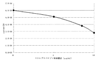
(2)例1A.吸水性物質と電解質を含むパッドを用いての光電流検出(競合法)。
i.パッドの作製
0.4Mのテトラプロピルアンモニウムヨージド(NPr4I)を含む水溶液を調製した。この水溶液に43mm×16mmに切った厚さ0.9mmのブロッティング用ろ紙(アトー株式会社製)を浸漬させて、50℃で2時間乾燥させてパッドを得た。
(2) Example 1A . Photocurrent detection using a pad containing a water-absorbing substance and an electrolyte (competitive method).
i. Preparation of Pad An aqueous solution containing 0.4 M tetrapropylammonium iodide (NPr 4 I) was prepared. A 0.9 mm-thick blotting filter paper (manufactured by Ato Co., Ltd.) cut into 43 mm × 16 mm was immersed in this aqueous solution and dried at 50 ° C. for 2 hours to obtain a pad.
ii.光電流測定
本実験で使用したセンサユニットの断面図および分解図を図12に示す。その実施の形態は上記(1)で作製したビオチン標識DNA固定化作用電極51と、ガラス板上に白金が蒸着されてなる対電極52とを用意した。両電極間に上記iで作製したパッド53を挟み、密着させた。その後、競合物質と想定した10μg/mlに調製したローダミン標識ストレプトアビジン溶液(溶媒組成:10mM HEPES P.H.7.4、150mM NaCl、0.05%Tween溶液)と被検物質と想定した10μg/ml、1μg/ml、0μg/mlに調製したストレプトアビジン溶液(溶媒組成:10mM HEPES P.H.7.4、150mM NaCl、0.05%Tween溶液)を1:1に混合させて作製した混合液54を500μlそれぞれパッドの端部に滴下し染み込ませた。この時、作用電極のDNAが固定化された面と対電極の白金蒸着面とが対向するように配置した。両電極を電気化学アナライザーに接続した状態で、作用電極にレーザー光源55(出力60mW、照射領域の直径1mm、波長530nmの緑色レーザー)を照射し、その時に観察される電流値を記録した。なお、図12中の56は押さえ部材、57は対向部材、58は電解質、59はビオチン標識DNA、60はローダミン標識ストレプトアビジン、61はストレプトアビジンを示す。
ii. Photocurrent measurement FIG. 12 shows a sectional view and an exploded view of the sensor unit used in this experiment. In the embodiment, a biotin-labeled DNA
結果を図13に示す。図13に示されるように、滴下した混合液54中のストレプトアビジン溶液の濃度が増加すると、光電流の減少が認められた。 The results are shown in FIG. As shown in FIG. 13, when the concentration of the streptavidin solution in the dropped mixed liquid 54 increased, a decrease in photocurrent was observed.
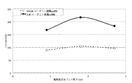
(3)例1B.吸水性物質、電解質、増感色素が標識された親和性物質を含むパッドを用いての光電流検出(競合法)
i.パッドの作製
0.4Mのテトラプロピルアンモニウムヨージド(NPr4I)を含む水溶液を調製した。この水溶液に43mm×16mmに切った厚さ0.9mmのブロッティング用ろ紙(アトー株式会社製)を浸漬させて、50℃で2時間乾燥させてパッド(1)を得た。その後、10μg/mlに調製したローダミン標識ストレプトアビジン溶液(溶媒組成:10mM HEPES P.H.7.4、150mM NaCl、0.05%Tween溶液)500μlを31mm×16mmに切った厚さ0.9mmのブロッティング用ろ紙(アトー株式会社製)に滴下し、50℃で2時間乾燥させてパッド(2)を得た。
(3) Example 1B. Photocurrent detection using a pad containing an affinity substance labeled with a water-absorbing substance, electrolyte, or sensitizing dye (competitive method)
i. Preparation of Pad An aqueous solution containing 0.4 M tetrapropylammonium iodide (NPr 4 I) was prepared. A 0.9 mm thick blotting filter paper (Ato Co., Ltd.) cut into 43 mm × 16 mm was immersed in this aqueous solution and dried at 50 ° C. for 2 hours to obtain a pad (1). Thereafter, rhodamine-labeled streptavidin solution (solvent composition: 10 mM HEPES PH7.4, 150 mM NaCl, 0.05% Tween solution) 500 μl prepared to 10 μg / ml was cut into 31 mm × 16 mm 0.9 mm thick blotting filter paper (Ato shares) Was added dropwise to the company) and dried at 50 ° C. for 2 hours to obtain a pad (2).
ii.光電流測定
本実験で使用したセンサユニットの断面図および分解図を図14に示す。その実施の形態は上記(1)で作製したビオチン標識DNA固定化作用電極51´と、ガラス板上に白金が蒸着されてなる対電極52´とを用意した。パッド(1)53´−aを対電極側に、パッド(2)53´−bを作用電極側に挟み、密着させた。その後、被検物質と想定した10μg/ml、1μg/ml、0μg/mlに調製したストレプトアビジン溶液(溶媒組成:10mM HEPES P.H.7.4、150mM NaCl、0.05%Tween溶液)54´を700μlずつパッド(2)の端部に滴下し、パッド(1)、パッド(2)に水を染み込ませた。この時、作用電極のDNAが固定化された面と対電極の白金蒸着面とが対向するように配置した。両電極を電気化学アナライザーに接続した状態で、作用電極にレーザー光源55´(出力60mW、照射領域の直径1mm、波長530nmの緑色レーザー)を照射し、その時に観察される電流値を記録した。なお、図14中の56´は押さえ部材、57´は対向部材、58´は電解質、59´はビオチン標識DNA、60´はローダミン標識ストレプトアビジン、61´はストレプトアビジンを示す。
ii. Photocurrent measurement FIG. 14 shows a sectional view and an exploded view of the sensor unit used in this experiment. In the embodiment, a biotin-labeled DNA-immobilizing working
結果を図15に示す。図15に示されるように、滴下した溶液中のストレプトアビジン濃度が高くなると、光電流が減少した。さらに、複数のパッドを用いても、検出可能であることが明らかになった。 The results are shown in FIG. As shown in FIG. 15, the photocurrent decreased as the streptavidin concentration in the dropped solution increased. Furthermore, it has been found that detection is possible even using a plurality of pads.
例2.DNA検出による電解質含有パッドの条件検討(参考例)
(1)色素標識DNA固定化作用電極の作製
作用電極用のガラス基材として、フッ素をドープした酸化スズ(F-SnO2:FTO)コートガラス(エイアイ特殊硝子社製、U膜、シート抵抗:12Ω/□、形状:50mm×26mm)を用意した。このガラス基材をアセトン中で15分間、続いて超純水中で15分間超音波洗浄を施して、汚れおよび残存有機物の除去を行った。このガラス基材を5Mの水酸化ナトリウム水溶液中で15分間振盪させた。その後、水酸化ナトリウムの除去のために超純水中での5分間の振盪を水を入れ替えて3回行った。ガラス基材を取り出して空気を吹き付けて残水を飛散させた後、ガラス基材を無水メタノールに浸漬させて脱水した。
Example 2. Examination of conditions for electrolyte-containing pads by DNA detection (reference example)
(1) Production of dye-labeled DNA-immobilized working electrode As a glass substrate for the working electrode, fluorine-doped tin oxide (F-SnO 2 : FTO) coated glass (manufactured by AI Special Glass Co., Ltd., U film, sheet resistance: 12Ω / □, shape: 50 mm × 26 mm) was prepared. This glass substrate was subjected to ultrasonic cleaning in acetone for 15 minutes and then in ultrapure water for 15 minutes to remove dirt and residual organic matter. The glass substrate was shaken in 5M aqueous sodium hydroxide solution for 15 minutes. Then, for removal of sodium hydroxide, shaking for 5 minutes in ultrapure water was performed 3 times with the water changed. After the glass substrate was taken out and air was blown to scatter the remaining water, the glass substrate was immersed in anhydrous methanol for dehydration.
95%メタノール5%超純水を溶媒として、3-アミノプロピルトリメトキシシラン(APTMS)を2vol%となるように加え、室温下で5分間の攪拌を行って、カップリング処理用の溶液を調製した。このカップリング処理用溶液に上記ガラス基材を浸漬させ、ゆっくりと15分間振盪させた。次いで、ガラス基材を取り出し、メタノール中で10回ほど振盪させて余剰なカップリング処理用溶液を除く操作を、メタノールを3回換えて行った。その後、ガラス基材を110度で30分間保持してカップリング剤をガラス基材に結合させた。ガラス基材を室温下で冷却した後、直径3mmの大きさの開口部が形成された粘着性シール(厚さ:0.5mm)を載置して密着させた。続いて、100 nMに濃度調整した5´末端ローダミン標識ssDNA(25mer)と、100 nMに濃度調整した非標識ssDNA(24mer)を95度で10分間保持した後、直ちに氷上に移して10分間保持してDNAを変性させた。この変性DNAを先に用意したガラス上のシールの開口部にそれぞれ5μlずつ充填し、95度で10分保持して溶媒を蒸発させた。その後、UVクロスリンカー(UVP社CL-1000型)で120mJの紫外光を照射して、標識ssDNA及び非標識ssDNAを各ガラス基材に固定化した。シールを各ガラス基材から剥がし、各ガラス基材を0.2%SDS溶液中で15分間×3回振盪させ、超純水を3回入れ替えて濯いだ。これらのガラス基材を沸騰水に2分間浸漬させて取り出した後、空気を吹き付けて残水を飛散させた。続いて、各ガラス基材を4度の無水エタノールに1分間浸漬させて脱水し、空気を吹き付けて残留エタノールを飛散させた。こうして、色素標識DNA固定化作用電極、ssDNA固定化作用電極を得た。ここで使用したプローブDNAの塩基配列は下記の通りである。
5´末端ローダミン標識ssDNA(プローブ1):5´-Rho-GCGGCATGAACCTGAGGCCCATCCT-3´
非標識ssDNA(プローブ2):5´-TTGAGCAAGTTCAGCCTGGTTAAG-3´
Using 95% methanol and 5% ultrapure water as a solvent, add 3-aminopropyltrimethoxysilane (APTMS) to 2vol% and stir at room temperature for 5 minutes to prepare a solution for coupling treatment did. The glass substrate was immersed in this coupling treatment solution and slowly shaken for 15 minutes. Subsequently, the glass substrate was taken out and shaken in methanol about 10 times to remove excess coupling solution, and the methanol was changed 3 times. Thereafter, the glass substrate was held at 110 degrees for 30 minutes to bond the coupling agent to the glass substrate. After the glass substrate was cooled at room temperature, an adhesive seal (thickness: 0.5 mm) in which an opening having a diameter of 3 mm was formed was placed and adhered. Subsequently, 5′-end rhodamine labeled ssDNA (25mer) adjusted to 100 nM and unlabeled ssDNA (24mer) adjusted to 100 nM were held at 95 ° C. for 10 minutes, then immediately transferred to ice and held for 10 minutes. Then, the DNA was denatured. The denatured DNA was filled in 5 μl each in the opening of the previously prepared seal on the glass and kept at 95 ° C. for 10 minutes to evaporate the solvent. Then, 120 mJ ultraviolet light was irradiated with a UV crosslinker (UVP CL-1000 type) to immobilize the labeled ssDNA and unlabeled ssDNA on each glass substrate. The seal was peeled off from each glass substrate, and each glass substrate was shaken in a 0.2% SDS solution for 15 minutes × 3 times, and rinsed by changing the ultrapure water three times. These glass substrates were immersed in boiling water for 2 minutes and taken out, and then air was blown to scatter the remaining water. Subsequently, each glass substrate was immersed in 4 degrees of absolute ethanol for 1 minute to dehydrate, and air was blown to disperse residual ethanol. Thus, a dye-labeled DNA immobilization working electrode and an ssDNA immobilization working electrode were obtained. The base sequence of the probe DNA used here is as follows.
5'-end rhodamine labeled ssDNA (probe 1): 5'-Rho-GCGGCATGAACCTGAGGCCCATCCT-3 '
Unlabeled ssDNA (probe 2): 5´-TTGAGCAAGTTCAGCCTGGTTAAG-3´
(2)電解質含有パッドの作製
0.2M、0.4M、および0.6Mのテトラプロピルアンモニウムヨージド(NPr4I)を含む水溶液を調製した。この水溶液に26mm×20mmに切った厚さ0.9mmのブロッティング用ろ紙(CB-13A;アトー株式会社)を浸漬させて、軽く水切りをし、電解質含有パッドを得た。
(2) Production of Electrolyte-Containing Pad Aqueous solutions containing 0.2M, 0.4M, and 0.6M tetrapropylammonium iodide (NPr 4 I) were prepared. A 0.9 mm-thick blotting filter paper (CB-13A; Ato Co., Ltd.) cut to 26 mm × 20 mm was dipped in this aqueous solution, and lightly drained to obtain an electrolyte-containing pad.
(3)例2A.電解質濃度の検討
上記(1)で作製した色素標識DNA固定化作用電極と、ガラス板上に白金が蒸着されてなる対電極とを用意した。両電極間に上記(2)で作製した電解質含有パッドを挟み、密着させた。この時、作用電極のssDNAが固定化された面と対電極の白金蒸着面とが対向するように配置した。両電極を電気化学アナライザーに接続した状態で、作用電極にレーザー光源(出力60mW、照射領域の直径1mm、波長530nmの緑色レーザー)を照射し、その時に観察される電流値を記録した。
(3) Example 2A . Examination of electrolyte concentration A dye-labeled DNA-immobilized working electrode prepared in the above (1) and a counter electrode obtained by depositing platinum on a glass plate were prepared. The electrolyte-containing pad produced in the above (2) was sandwiched between the electrodes and adhered. At this time, the working electrode was placed so that the surface on which the ssDNA was immobilized was opposed to the platinum deposition surface of the counter electrode. With both electrodes connected to the electrochemical analyzer, the working electrode was irradiated with a laser light source (
結果を図16に示す。図16に示されるように、テトラプロピルアンモニウムヨージドの濃度に依存して光電流の増加が認められたが、いずれの濃度のテトラプロピルアンモニウムヨージドおいても測定に使用可能であることが明らかになった。 The results are shown in FIG. As shown in FIG. 16, an increase in photocurrent was observed depending on the concentration of tetrapropylammonium iodide, but it is clear that any concentration of tetrapropylammonium iodide can be used for measurement. Became.
(4)例2B.各種電解質の検討
各種電解質を用いて光電流測定を行った。具体的には、吸水性物質としてろ紙を用い、各還元剤の濃度を0.2Mに固定して、電解質含有パッドを作製した。電解質としては、NaI、KI、CaI2、LiI、NH4I、テトラプロピルアンモニウムヨージド(NPr4I)、チオ硫酸ナトリウム(Na2S2O3)および亜硫酸ナトリウム(Na2SO3)を用いた。これらの各種電解質と水を含む電解液を作製し、26mm×20mmに切った厚さ0.9mmのブロッティング用ろ紙(CB-13A;アトー株式会社)を浸漬させて、軽く水切りをし、電解質含有パッドを得た。色素標識DNA固定化作用電極の作製は(1)と同様にして行い、ローダミン標識ssDNA濃度が10nM、およびローダミン非標識ssDNA濃度100nMの各溶液を用いて作製した作用電極も作製して(3)と同様に光電流測定を行った。
(4) Example 2B . Examination of various electrolytes Photocurrent measurement was performed using various electrolytes. Specifically, a filter paper was used as the water-absorbing substance, and the concentration of each reducing agent was fixed at 0.2 M to prepare an electrolyte-containing pad. As the electrolyte, use NaI, KI, CaI 2, LiI , NH 4 I, tetrapropylammonium iodide (NPr 4 I), sodium thiosulfate (Na 2 S 2 O 3) and
結果を図17に示す。図17に示されるように、検討したいずれの電解質でも、ssDNA固定化量に依存して光電流の増加が認められ、測定に使用可能であることが明らかになった。 The results are shown in FIG. As shown in FIG. 17, in any of the studied electrolytes, an increase in photocurrent was recognized depending on the amount of immobilized ssDNA, and it was revealed that it can be used for measurement.
(5)例2C.電解質含有パッドの厚さの検討
固定化するssDNA濃度を100nMと1μMの2濃度としたこと以外は(1)と同様にして、色素標識DNA固定化作用電極を作製した後、0.2Mの濃度のテトラプロピルアンモニウムヨージド(NPr4I)と水により電解液を作製し、厚さ0.9mmのブロッティング用ろ紙(CB-13A;アトー株式会社)を1枚、2枚重ね、3枚重ねし、それぞれ電解液に浸漬させて電解質含有パッドを作製した。その後、作製した固定化濃度の異なる作用電極と、厚さの異なる各電解質含有パッドを用いて、(3)と同様にして光電流を測定した。
(5) Example 2C . Examination of the thickness of the electrolyte-containing pad After preparing the dye-labeled DNA-immobilizing working electrode in the same manner as (1) except that the ssDNA concentration to be immobilized was changed to two concentrations of 100 nM and 1 μM, the concentration of 0.2 M Prepare an electrolyte with tetrapropylammonium iodide (NPr 4 I) and water, and stack one, two or three sheets of 0.9 mm thick blotting filter paper (CB-13A; Ato Co., Ltd.) An electrolyte-containing pad was prepared by dipping in an electrolytic solution. Thereafter, the photocurrent was measured in the same manner as in (3) using the prepared working electrodes having different immobilization concentrations and respective electrolyte-containing pads having different thicknesses.
結果を図18に示す。図18に示されるように、0.9mm〜2.7mmの電解質含有パッド厚さの全域にわたって、光電流値への影響はほとんど認められなかった。したがって、十分な強度を得る観点から電解質含有パッド厚さを厚くしても、光電流値検出への悪影響は無いことが推察される。 The results are shown in FIG. As shown in FIG. 18, almost no influence on the photocurrent value was observed over the entire area of the electrolyte-containing pad thickness of 0.9 mm to 2.7 mm. Therefore, it is presumed that there is no adverse effect on the detection of the photocurrent value even if the electrolyte-containing pad thickness is increased from the viewpoint of obtaining sufficient strength.
(6)例2D.各種パッドの検討
厚さ0.9mmのブロッティング用ろ紙(CB-13A;アトー株式会社)、フェルト(厚さ:1mm、密度:0.00049g/mm3)、ボール紙(厚さ:0.5mm、密度:0.00071g/mm3)、ガラス繊維ろ紙(GF/D;Whatman:厚さ:0.68mm)、パルプ繊維及び合成繊維を含むコート紙(厚さ:0.14mm、密度:0.00111g/mm3)、弗素樹脂を主に含んでなるメンブレンフィルター(JCWP09025;MILLIPORE:厚さ:0.1mm)を用いた以外は(3)と同様にして光電流の測定を行った。色素標識DNA固定化作用電極の作製は(1)と同様にして行い、ローダミン標識ssDNA濃度が100nM、および1μMの各溶液と、非標識ssDNA濃度が100nMを用いて作製した作用電極も作製して(1)同様に光電流測定を行った。電解液は0.2Mのテトラプロピルアンモニウムヨージド(NPr4I)を含む水溶液を用いた。
(6) Example 2D . Examination of various pads Blotting filter paper (CB-13A; ATTO Co., Ltd.) having a thickness of 0.9 mm, felt (thickness: 1 mm, density: 0.00049 g / mm 3 ), cardboard (thickness: 0.5 mm, density: 0.00071) g / mm 3 ), glass fiber filter paper (GF / D; Whatman: thickness: 0.68 mm), coated paper containing pulp fiber and synthetic fiber (thickness: 0.14 mm, density: 0.00111 g / mm 3 ), fluorine resin The photocurrent was measured in the same manner as (3) except that a membrane filter (JCWP09025; MILLIPORE: thickness: 0.1 mm) mainly containing The dye-labeled DNA-immobilized working electrode was prepared in the same manner as (1), and a working electrode prepared using each solution with rhodamine-labeled ssDNA concentrations of 100 nM and 1 μM and an unlabeled ssDNA concentration of 100 nM was also prepared. (1) Photocurrent measurement was performed in the same manner. As the electrolytic solution, an aqueous solution containing 0.2 M tetrapropylammonium iodide (NPr 4 I) was used.
結果を図19に示す。図19に示されるように、すべてのパッドにおいて、ssDNA固定化量に依存して光電流の増加が認められ、電解質含有パッドとして使用可能であることが明らかになった。 The results are shown in FIG. As shown in FIG. 19, in all the pads, an increase in photocurrent was observed depending on the amount of immobilized ssDNA, and it was revealed that the pads can be used as electrolyte-containing pads.
(7)例2E.電解質含有パッドの含水率の検討
i.含水率の測定
まず、26mm×20mmに切った厚さ0.9mmのブロッティング用ろ紙(CB-13A;アトー株式会社)に0.4Mのテトラプロピルアンモニウムヨージド(NPr4I)を含む水溶液を500μl滴下し、ろ紙を完全に電解液に浸した。こうして、電解液が含浸されたろ紙を作製した。次に、各含浸されたろ紙を0時間、0.25時間、0.5時間、1時間、1.25時間、1.5時間、それぞれ50度で乾燥させた。乾燥後のろ紙の重量を測定し、テトラプロピルアンモニウムヨージドの重量を除いた後、1mm3 辺りの含水量を計算した。その後、(1mm3 辺りの含水量)/(ろ紙密度)の割合を計算し電解質含有パッドの含水率とした。なおブロッティング用ろ紙の密度は0.00049g/mm3である。
ii.光電流測定
i.で作製した各含水率の電解質含有パッドにより例1と同様にして光電流を検出した。
(7) Example 2E . Examination of moisture content of electrolyte-containing pad i. Measurement of water content First, 500 μl of an aqueous solution containing 0.4 M tetrapropylammonium iodide (NPr 4 I) was dropped on a 0.9 mm thick filter paper (CB-13A; Atto Co., Ltd.) cut to 26 mm × 20 mm. The filter paper was completely immersed in the electrolyte. Thus, a filter paper impregnated with the electrolytic solution was produced. Next, each impregnated filter paper was dried at 50 degrees for 0 hour, 0.25 hour, 0.5 hour, 1 hour, 1.25 hour and 1.5 hour, respectively. The weight of the filter paper after drying was measured, and after removing the weight of tetrapropylammonium iodide, the water content around 1 mm 3 was calculated. Thereafter, the ratio of (water content around 1 mm 3 ) / (filter paper density) was calculated and used as the water content of the electrolyte-containing pad. The density of the blotting filter paper is 0.00049 g / mm 3 .
ii. Photocurrent measurement i. The photocurrent was detected in the same manner as in Example 1 by using the electrolyte-containing pad having each moisture content prepared in (1).
結果を図20に示す。図20に示されるように、電解質含有パッドの含水率が高いほど、光電流が高いことがわかる。また、含水率が2.2%の時は光電流を検出できなかったが、含水率が25.3%の時には光電流が検出できた。以上のことから、光電流が検出可能な電解質含有パッドは、含水率が少なくとも20%以上であることが望ましい。
The results are shown in FIG. As shown in FIG. 20, it can be seen that the higher the moisture content of the electrolyte-containing pad, the higher the photocurrent. Photocurrent could not be detected when the water content was 2.2%, but photocurrent could be detected when the water content was 25.3%. From the above, it is desirable that the electrolyte-containing pad capable of detecting photocurrent has a water content of at least 20% or more.
Claims (19)
電解質存在下、前記作用電極に光を照射して前記増感色素を光励起させ、該光励起された増感色素から前記作用電極への電子移動に起因して前記作用電極と前記対電極との間に流れる光電流を検出することにより、被検物質を特異的に検出する方法であって、
前記結合は、
被検物質が直接または間接的に結合可能なプローブ物質を表面に備えた作用電極を前記パッドに接触させ、
被検物質および溶媒を少なくとも含有してなる試料液を前記パッドに含浸させて行われ、
前記増感色素および前記電解質は、それぞれ前記試料液またはパッドのいずれかに含有される、方法。 A working electrode comprising a probe substance specifically bound to the test substance directly or indirectly on the surface, and a sensitizing dye fixed by the binding, and a counter electrode were brought into contact with a water-absorbing pad. In state,
In the presence of an electrolyte, the working electrode is irradiated with light to photoexcite the sensitizing dye, and between the working electrode and the counter electrode due to electron transfer from the photoexcited sensitizing dye to the working electrode. A method for specifically detecting a test substance by detecting a photocurrent flowing through
The bond is
A working electrode provided on the surface with a probe substance to which a test substance can be directly or indirectly bound is brought into contact with the pad;
It is carried out by impregnating the pad with a sample solution containing at least a test substance and a solvent,
The sensitizing dye and the electrolyte are each contained in either the sample solution or the pad.
The method according to claim 1, wherein the sensitizing dye is labeled with an affinity substance capable of specific binding directly or indirectly with a probe substance.
吸水性物質を少なくとも含んでなる、パッド。 It is a pad used for a method given in any 1 paragraph of Claims 1-4,
A pad comprising at least a water-absorbing substance.
作用電極と、
前記作用電極および対電極の間に挟持される請求項5〜10に記載のパッドと
を備えてなり、前記作用電極の表面が前記パッドと接触してなる、センサユニット。 A sensor unit used for specific detection of a test substance using a photocurrent generated by photoexcitation of a sensitizing dye,
A working electrode;
A sensor unit comprising the pad according to claim 5 sandwiched between the working electrode and a counter electrode, wherein the surface of the working electrode is in contact with the pad.
前記支持基材に向けて、前記作用電極、前記パッド、および前記対電極を互いに密着させるように押さえる押さえ部材と
をさらに備えてなる、請求項12に記載のセンサユニット。 A support substrate for supporting the counter electrode;
The sensor unit according to claim 12, further comprising a pressing member that presses the working electrode, the pad, and the counter electrode in close contact with each other toward the support base.
作用電極および対電極が同一平面上にパターニングされてなる電極ユニットと、
前記作用電極および前記対電極の各電極表面に接触して設けられる、請求項5〜10に記載のパッドを備えてなる、センサユニット。 A sensor unit used for specific detection of a test substance using a photocurrent generated by photoexcitation of a sensitizing dye,
An electrode unit in which the working electrode and the counter electrode are patterned on the same plane;
A sensor unit comprising the pad according to claim 5, which is provided in contact with each electrode surface of the working electrode and the counter electrode.
前記電極ユニットと前記対向部材との間に前記パッドが挟持される、請求項14に記載のセンサユニット。 Further comprising a facing member provided facing the electrode unit;
The sensor unit according to claim 14, wherein the pad is sandwiched between the electrode unit and the facing member.
前記対向部材が、前記支持基材に向けて、前記パッドおよび前記電極ユニットを互いに密着させるように押さえる押さえ部材として機能する、請求項15に記載のセンサユニット。 Further comprising a support substrate for supporting the electrode unit, and
The sensor unit according to claim 15, wherein the facing member functions as a pressing member that presses the pad and the electrode unit toward each other toward the support base material.
前記支持基材に向けて、前記電極ユニットを密着させるように押さえる押さえ部材とをさらに備えてなり、
前記パッドが前記電極ユニット上に載置されてなる、請求項14に記載のセンサユニット。 A support substrate for supporting the electrode unit;
A pressing member that holds the electrode unit in close contact with the supporting base material,
The sensor unit according to claim 14, wherein the pad is placed on the electrode unit.
請求項11〜18のいずれか一項に記載されるセンサユニットと、
前記作用電極に光を照射するための光源と、
前記作用電極と前記対電極との間を流れる電流を測定する電流計と
を備えた、測定装置。 A measuring device used for specific detection of a test substance using a photocurrent generated by photoexcitation of a sensitizing dye,
A sensor unit according to any one of claims 11 to 18,
A light source for irradiating the working electrode with light;
A measuring apparatus comprising: an ammeter that measures a current flowing between the working electrode and the counter electrode.
Priority Applications (1)
| Application Number | Priority Date | Filing Date | Title |
|---|---|---|---|
| JP2007037181A JP2008202995A (en) | 2007-02-16 | 2007-02-16 | Specific detecting method of substance to be inspected using photocurrent, pad used therein, sensor unit, and measuring instrument |
Applications Claiming Priority (1)
| Application Number | Priority Date | Filing Date | Title |
|---|---|---|---|
| JP2007037181A JP2008202995A (en) | 2007-02-16 | 2007-02-16 | Specific detecting method of substance to be inspected using photocurrent, pad used therein, sensor unit, and measuring instrument |
Publications (1)
| Publication Number | Publication Date |
|---|---|
| JP2008202995A true JP2008202995A (en) | 2008-09-04 |
Family
ID=39780682
Family Applications (1)
| Application Number | Title | Priority Date | Filing Date |
|---|---|---|---|
| JP2007037181A Pending JP2008202995A (en) | 2007-02-16 | 2007-02-16 | Specific detecting method of substance to be inspected using photocurrent, pad used therein, sensor unit, and measuring instrument |
Country Status (1)
| Country | Link |
|---|---|
| JP (1) | JP2008202995A (en) |
Cited By (1)
| Publication number | Priority date | Publication date | Assignee | Title |
|---|---|---|---|---|
| WO2013047624A1 (en) | 2011-09-26 | 2013-04-04 | Toto株式会社 | Method for specifically detecting test substance |
-
2007
- 2007-02-16 JP JP2007037181A patent/JP2008202995A/en active Pending
Cited By (1)
| Publication number | Priority date | Publication date | Assignee | Title |
|---|---|---|---|---|
| WO2013047624A1 (en) | 2011-09-26 | 2013-04-04 | Toto株式会社 | Method for specifically detecting test substance |
Similar Documents
| Publication | Publication Date | Title |
|---|---|---|
| US8092670B2 (en) | Method for specifically detecting analyte using photocurrent, and electrode, measuring cell and measuring device for use therein | |
| US20090205979A1 (en) | Electrolyte-Containing Sheet For Use In Specific Detection Of Analyte Using Photocurrent | |
| JP5344079B2 (en) | Electrode member used for specific detection of test substance by photocurrent | |
| JP2006119111A (en) | Specific detection method for test substance using photocurrent, electrode used therefor, measuring cell and measurement device | |
| JP4826860B2 (en) | Measuring device used for specific detection of test substance using photocurrent, sensor unit used therefor, and specific detection method of test substance using photocurrent | |
| WO2009088082A1 (en) | Method for specifically detecting test substance using photocurrent, sensor unit used therefor, and measuring device | |
| JP4873219B2 (en) | Electrode unit used for specific detection of test substance using photocurrent generated by photoexcitation of sensitizing dye, and sensor cell and measurement apparatus using the same | |
| JP2008020205A (en) | Gel sheet used for specifically detecting test material using photocurrent, detection method using it, sensor unit and measuring instrument | |
| JP4735860B2 (en) | Specific detection method of test substance using photocurrent, electrode used therefor, measuring cell and measuring apparatus | |
| CN103913571A (en) | Immunodetection method of array breakage electrode | |
| JP4919101B2 (en) | Sensor cell and measuring device used for specific detection of test substance using photocurrent generated by photoexcitation of sensitizing dye | |
| WO2005093418A1 (en) | Method of specifically detecting test substance by using photocurrent and electrodes, measurement cell, measurement device and buffer solution to be used therefor | |
| JP4831524B2 (en) | Sensor cell and measuring device used for specific detection of test substance using photocurrent generated by photoexcitation of sensitizing dye | |
| JP2008202995A (en) | Specific detecting method of substance to be inspected using photocurrent, pad used therein, sensor unit, and measuring instrument | |
| JP2006284413A (en) | Blocking agent for pigment sensitization type biosensor | |
| JP2008157916A (en) | Water-bearing sheet used in specific detection of substance to be inspected using photocurrent, detection method using the sheet, sensor unit and measuring instrument | |
| JP2009186453A (en) | Sensor unit used for specifically detecting tested substance by using photoelectric current and measuring instrument using same | |
| JP2009186454A (en) | Sensor unit used for specifically detecting tested substance by using photoelectric current and measuring instrument using same | |
| CN113984684A (en) | Photoelectric immunosensor for detecting Alzheimer's disease marker and preparation method and application thereof | |
| JP2010038813A (en) | Sensor chip used for specific detection of substance to be inspected using photoelectric current, and measurement device using the same | |
| JP2008192770A (en) | Sensor chip to be used for specifically detecting test substance using photocurrent, and measuring apparatus using the same | |
| JP2006090893A (en) | Buffer solution used in contact with acting electrode used in specific detection of substance to be inspected, using photocurrent generated by optical excitation of sensitizing dye |