JP2008197398A - Optical element package, backlight and liquid crystal display - Google Patents
Optical element package, backlight and liquid crystal display Download PDFInfo
- Publication number
- JP2008197398A JP2008197398A JP2007032767A JP2007032767A JP2008197398A JP 2008197398 A JP2008197398 A JP 2008197398A JP 2007032767 A JP2007032767 A JP 2007032767A JP 2007032767 A JP2007032767 A JP 2007032767A JP 2008197398 A JP2008197398 A JP 2008197398A
- Authority
- JP
- Japan
- Prior art keywords
- optical element
- support
- light
- liquid crystal
- incident
- Prior art date
- Legal status (The legal status is an assumption and is not a legal conclusion. Google has not performed a legal analysis and makes no representation as to the accuracy of the status listed.)
- Pending
Links
Images


Landscapes
- Liquid Crystal (AREA)
- Planar Illumination Modules (AREA)
- Devices For Indicating Variable Information By Combining Individual Elements (AREA)
Abstract
Description
この発明は、光学素子包装体、ならびにそれを備えるバックライトおよび液晶表示装置に関する。詳しくは、液晶表示装置の表示特性を改善する光学素子包装体に関する。 The present invention relates to an optical element package, and a backlight and a liquid crystal display device including the same. Specifically, the present invention relates to an optical element package that improves display characteristics of a liquid crystal display device.
従来、液晶表示装置では、視野角や輝度などの改善を目的として多数の光学素子が用いられている。これらの光学素子としては、拡散フィルムやプリズムシートなどのフィルム状やシート状のものが用いられている。 Conventionally, in a liquid crystal display device, a large number of optical elements are used for the purpose of improving the viewing angle and the luminance. As these optical elements, film-like or sheet-like materials such as a diffusion film and a prism sheet are used.
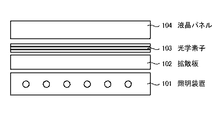
図31は、従来の液晶表示装置の構成を示す。この液晶表示装置は、図31に示すように、光を出射する照明装置101と、照明装置101から出射された光の拡散する拡散板102と、拡散板102により拡散された光を集光や拡散などする複数の光学素子103と、液晶パネル104とを備える。 FIG. 31 shows a configuration of a conventional liquid crystal display device. As shown in FIG. 31, the liquid crystal display device includes an illuminating device 101 that emits light, a diffusion plate 102 that diffuses light emitted from the illuminating device 101, and condensing light diffused by the diffusing plate 102. A plurality of optical elements 103 for diffusing and a liquid crystal panel 104 are provided.
ところで、近年の画像表示装置の大型化に伴って、光学素子の自重やサイズが増大する傾向にある。このように光学素子の自重やサイズの増大すると、光学素子の剛性が不足するため、光学素子の変形が発生してしまう。このような光学素子の変形は、表示面への光学指向性に影響を与え、輝度ムラという重大な問題を招いてしまう。 By the way, with the recent increase in size of image display devices, the weight and size of optical elements tend to increase. If the weight or size of the optical element increases as described above, the optical element is insufficiently rigid, and the optical element is deformed. Such deformation of the optical element affects the optical directivity on the display surface and causes a serious problem of luminance unevenness.
そこで、光学素子の厚さ増すことで、光学素子の剛性不足を改善することが提案されている。しかしながら、液晶表示装置が厚くなってしまい、薄型かつ軽量という液晶表示装置の利点が損なわれてしまう。そこで、光学素子同士を透明粘着剤により貼り合わせることにより、シート状またはフォルム状の光学素子の剛性不足を改善することが提案されている(例えば特許文献1参照)。 Accordingly, it has been proposed to improve the rigidity of the optical element by increasing the thickness of the optical element. However, the liquid crystal display device becomes thick, and the advantages of the thin and lightweight liquid crystal display device are impaired. Thus, it has been proposed to improve the lack of rigidity of a sheet-like or form-like optical element by bonding optical elements together with a transparent adhesive (see, for example, Patent Document 1).
しかしながら、特許文献1の技術では、光学素子同士を透明粘着剤により貼り合わせるため、光学素子の厚さが増し、液晶表示装置自体が厚くなってしまう。更には、液晶表示装置に必須である光学機能を発現させるには、粘着剤を使用することによって、集光機能層、拡散機能層らと隣接する光学機能層との構造体間が埋設されてしまい、その結果、光学機能が損なわれ、表示特性が劣化してしまう。
However, in the technique of
したがって、この発明の目的は、液晶表示装置の厚みの増加、または液晶表示装置の表示特性の劣化を抑えつつ、光学素子の剛性不足を改善することができる光学素子包装体、ならびにそれを備えるバックライトおよび液晶表示装置を提供することにある。 Accordingly, an object of the present invention is to provide an optical element package that can improve the lack of rigidity of an optical element while suppressing an increase in thickness of the liquid crystal display apparatus or deterioration of display characteristics of the liquid crystal display apparatus, and a bag including the same. It is to provide a light and a liquid crystal display device.
本発明者らは、従来技術が有する上述の課題を解決すべく、鋭意検討を行った。以下にその概要を説明する。 The present inventors have intensively studied to solve the above-described problems of the prior art. The outline will be described below.
本発明者らは、液晶表示装置の厚みの増加、または液晶表示装置の表示特性の劣化を抑えつつ、光学素子の剛性不足を改善すべく、鋭意検討を行った結果、光学素子および支持体を包装部材により包装してなる光学素子包装体を発明するに至った。 As a result of intensive studies to improve the rigidity of the optical element while suppressing the increase in the thickness of the liquid crystal display device or the deterioration of the display characteristics of the liquid crystal display device, the present inventors have determined that the optical element and the support are It came to invent the optical element packaging body formed by packaging with a packaging member.
しかしながら、本発明者らの知見によれば、光源から発せられる熱や液晶表示装置の使用環境によっては、包装部材に撓みなどが発生する場合がある。そこで、この撓みなどの発生を抑制すべく、本発明者らは鋭意検討を行った。その結果、本発明者らは支持体に凸面などを設けることを見出すに至った。
本発明は以上の検討に基づいて案出されたものである。
However, according to the knowledge of the present inventors, the packaging member may be bent depending on the heat generated from the light source or the usage environment of the liquid crystal display device. Therefore, the present inventors have intensively studied to suppress the occurrence of this bending and the like. As a result, the present inventors have found that the support is provided with a convex surface or the like.
The present invention has been devised based on the above studies.
上述の課題を解決するために、第1の発明は、
1または2以上光学素子と、
1または2以上の光学素子を支持する支持体と、
1または2以上の光学素子および支持体を包む包装部材と
を備え、
支持体は、
光源からの光が入射する入射面と、
第1の面から入射した光を液晶パネルに向けて出射する出射面と
を有し、
入射面および出射面の少なくとも一方の面が、凹形状または凸形状であることを特徴とする光学素子包装体である。
In order to solve the above-mentioned problem, the first invention
One or more optical elements;
A support that supports one or more optical elements;
A packaging member that wraps one or more optical elements and a support,
The support is
An incident surface on which light from the light source is incident;
An exit surface that emits light incident from the first surface toward the liquid crystal panel;
At least one of the entrance surface and the exit surface has a concave shape or a convex shape.
第2の発明は、
光を出射する光源と、
光源から出射された光の特性を改善し、液晶パネルに対して出射する光学素子包装体と
を備え、
光学素子包装体は、
1または2以上光学素子と、
1または2以上の光学素子を支持する支持体と、
1または2以上の光学素子および支持体を包む包装部材と
を備え、
支持体は、
光源からの光が入射する入射面と、
第1の面から入射した光を液晶パネルに向けて出射する出射面と
を有し、
入射面および出射面の少なくとも一方の面が、凹形状または凸形状であることを特徴とするバックライトである。
The second invention is
A light source that emits light;
An optical element package that improves the characteristics of light emitted from the light source and emits light to the liquid crystal panel;
The optical element package is
One or more optical elements;
A support that supports one or more optical elements;
A packaging member that wraps one or more optical elements and a support,
The support is
An incident surface on which light from the light source is incident;
An exit surface that emits light incident from the first surface toward the liquid crystal panel;
The backlight is characterized in that at least one of the entrance surface and the exit surface is concave or convex.
第3の発明は、
光を出射する光源と、
光源から出射された光の特性を改善する光学素子包装体と、
光学素子包装体により特性が改善された光に基づき、画像を表示する液晶パネルと
を備え、
光学素子包装体は、
1または2以上光学素子と、
1または2以上の光学素子を支持する支持体と、
1または2以上の光学素子および支持体を包む包装部材と
を備え、
支持体は、
光源からの光が入射する入射面と、
入射面から入射した光を液晶パネルに向けて出射する出射面と
を有し、
入射面および出射面の少なくとも一方の面が、凹形状または凸形状であることを特徴とする液晶表示装置である。
The third invention is
A light source that emits light;
An optical element package for improving the characteristics of the light emitted from the light source;
A liquid crystal panel that displays an image based on light whose characteristics have been improved by the optical element package,
The optical element package is
One or more optical elements;
A support that supports one or more optical elements;
A packaging member that wraps one or more optical elements and a support,
The support is
An incident surface on which light from the light source is incident;
And an exit surface that emits light incident from the entrance surface toward the liquid crystal panel,
The liquid crystal display device is characterized in that at least one of an incident surface and an output surface has a concave shape or a convex shape.
第4の発明は、
光を出射する光源と、
光源から出射された光の特性を改善し、液晶パネルに対して出射する光学素子包装体と
を備え、
光学素子包装体は、
1または2以上光学素子と、
1または2以上の光学素子を支持する支持体と、
1または2以上の光学素子および支持体を包む包装部材と
を備え、
支持体は、
光源からの光が入射する入射面と、
入射面から入射した光を液晶パネルに向けて出射する出射面と
を有し、
出射面側の光学素子を支持体とすることを特徴とするバックライトである。
The fourth invention is:
A light source that emits light;
An optical element package that improves the characteristics of light emitted from the light source and emits light to the liquid crystal panel;
The optical element package is
One or more optical elements;
A support that supports one or more optical elements;
A packaging member that wraps one or more optical elements and a support,
The support is
An incident surface on which light from the light source is incident;
And an exit surface that emits light incident from the entrance surface toward the liquid crystal panel,
The backlight is characterized in that the optical element on the exit surface side is used as a support.
第5の発明は、
光を出射する光源と、
光源から出射された光の特性を改善する光学素子包装体と、
光学素子包装体により特性が改善された光に基づき、画像を表示する液晶パネルと
を備え、
光学素子包装体は、
1または2以上光学素子と、
1または2以上の光学素子を支持する支持体と、
1または2以上の光学素子および支持体を包む包装部材と
を備え、
支持体は、
光源からの光が入射する入射面と、
入射面から入射した光を液晶パネルに向けて出射する出射面と
を有し、
出射面側の光学素子を支持体とすることを特徴とする液晶表示装置である。
The fifth invention is:
A light source that emits light;
An optical element package for improving the characteristics of the light emitted from the light source;
A liquid crystal panel that displays an image based on light whose characteristics have been improved by the optical element package,
The optical element package is
One or more optical elements;
A support that supports one or more optical elements;
A packaging member that wraps one or more optical elements and a support,
The support is
An incident surface on which light from the light source is incident;
And an exit surface that emits light incident from the entrance surface toward the liquid crystal panel,
A liquid crystal display device characterized in that an optical element on the exit surface side is used as a support.
この発明では、1または2以上の光学素子と支持体とを包装部材により包んでいるので、1または2以上の光学素子と支持体とを一体化することができる。したがって、支持体により光学素子の剛性不足を補うことができる。また、支持体の入射面および出射面の少なくとも一方の面を凹形状または凸形状にしているので、包装部材の撓みを抑制することができる。 In the present invention, since one or more optical elements and the support are wrapped by the packaging member, the one or more optical elements and the support can be integrated. Therefore, the support member can compensate for the lack of rigidity of the optical element. Moreover, since at least one surface of the entrance surface and the exit surface of the support is concave or convex, it is possible to suppress the bending of the packaging member.
以上説明したように、この発明によれば、液晶表示装置の厚みの増加、または液晶表示装置の表示特性の劣化を抑えつつ、光学素子の剛性不足を改善することができる。また、包装部材の撓みを抑制することができるので、包装部材を備えた液晶表示装置の表示特性の低下を抑制できる。 As described above, according to the present invention, an insufficient rigidity of the optical element can be improved while suppressing an increase in the thickness of the liquid crystal display device or a deterioration in display characteristics of the liquid crystal display device. Moreover, since the bending of a packaging member can be suppressed, the fall of the display characteristic of the liquid crystal display device provided with the packaging member can be suppressed.
以下、この発明の実施形態について図面を参照しながら説明する。なお、以下の実施形態の全図においては、同一または対応する部分には同一の符号を付す。 Hereinafter, embodiments of the present invention will be described with reference to the drawings. In all the drawings of the following embodiments, the same or corresponding parts are denoted by the same reference numerals.
(1)第1の実施形態
(1−1)液晶表示装置の構成
図1は、この発明の第1の実施形態による液晶表示装置の一構成例を示す。この液晶表示装置は、図1に示すように、光を出射する照明装置1と、照明装置1から出射された光の特性を改善する光学素子包装体2と、光学素子包装体2により特性が改善された光に基づき、画像を表示する液晶パネル3とを備える。照明装置1と光学素子包装体2とによりバックライトが構成される。以下では、照明装置1からの光が入射する面を入射面、この入射面から入射した光を出射する面を出射面、および入射面と出射面との間に位置する面を端面と称する。また、入射面と出射面とを総称して主面と適宜称する。
(1) First Embodiment (1-1) Configuration of Liquid Crystal Display Device FIG. 1 shows a configuration example of a liquid crystal display device according to a first embodiment of the present invention. As shown in FIG. 1, the liquid crystal display device is characterized by the
照明装置1は、例えば直下式の照明装置であり、光を出射する光源11と、光源11から出射された光を反射して液晶パネル3の方向に向ける反射板12とを備える。光源11としては、例えば、冷陰極蛍光管(CCFL:Cold Cathode Fluorescent Lamp)、熱陰極蛍光管(HCFL:Hot Cathode Fluorescent Lamp)、有機エレクトロルミネッセンス(OEL:Organic ElectroLuminescence)または発光ダイオード(LED:Light Emitting Diode)などを用いることができる。反射板12は、例えば1または複数の光源11の下方および側方を覆うように設けられ、1または複数の光源11から下方および側方などに出射された光を反射して、液晶パネル3の方向に向けるためのものである。
The
光学素子包装体2は、例えば、照明装置1から出射された光を拡散や集光などの処理を施して光の特性を変える1または複数の光学素子24と、1または複数の光学素子を支持する支持体23と、1または複数の光学素子24と支持体23とを包んで一体化する包装部材22を備える。以下では、支持体23と1または複数の光学素子24とを重ね合わされたものを光学素子積層体21と称する。
The optical element package 2 supports, for example, one or a plurality of
光学素子24の数や種類は、特に限定されるのもではなく、所望とする液晶表示装置の特性に応じて適宜選択することができる。光学素子24としては、例えば支持体と1または複数の機能層からなるもの、もしくは、1または複数の機能層のみからなるものを用いることができる。光学素子24としては、例えば光拡散素子、光集光素子、反射型偏光子、偏光子または光分割素子などを用いることができる。光学素子としては、例えば、フィルム状、シート状または板状のものを用いることができる。光学素子24の厚さは、例えば5〜1000μmである。
The number and type of the
支持体23は、例えば、照明装置1から出射された光を透過する透明板、または照明装置1から出射された光に拡散や集光などの処理を施して光の特性を変える光学板である。光学板としては、例えば拡散板、位相差板またはプリズム板などを用いることができる。支持体23の厚さは、例えば1000〜50000μmである。支持体23は、例えば高分子材料からなり、その透過率は30%以上であることが好ましい。なお、光学素子24と支持体23との積層の順序は、例えば、光学素子24および支持体23の有する機能に応じて選ばれる。例えば、支持体23が拡散板である場合、支持体23は、照明装置1からの光が入射する側に設けられ、支持体23が反射型偏光板である場合、支持体23は、液晶パネル3に光を出射する側に設けられる。光学素子24および支持体23の入射面および出射面の形状は、液晶パネル3の形状に応じて選ばれ、例えば縦横比(アスペクト比)の異なる矩形状である。
The
光学素子24および支持体23の主面には、凹凸処理を施すこと、または微少粒子を含有させることが好ましい。こすれや摩擦を低減できるからである。また、光学素子24および支持体23には、必要に応じて光安定剤、紫外線吸収剤、帯電防止剤、難燃剤および酸化防止剤などの添加剤を含有させることにより、紫外線吸収機能、赤外線吸収機能および静電抑制機能などを光学素子24および支持体23に付与するようにしてもよい。また、光学素子24および支持体23には、アンチリフレクション処理(AR処理)やアンチグレア処理(AG処理)などの表面処理を施すことにより、反射光の拡散や反射光そのものの低減を図るようにしてもよい。また、光学素子24および支持体23の表面に、紫外線や赤外線を反射するための機能を持たせるようにしてもよい。
The main surfaces of the
包装部材22は、例えば透明性を有する単層または複数層のフィルム状、シート状もしくは袋状である。包装部材22は例えば帯状の形状を有し、その長手方向の端面同士が、好ましくは光学素子積層体21の端面上にて接合されている。なお、以下では、包装部材22の面のうち、光学素子積層体21の側となる面を内側面、それとは反対側の面を外側面と称する。
The
包装部材22のフィルムもしくはシートは、同一方向の長手方向で結合されていても、長手と交わる方向で結合されていてもよい。これらの包装部材22は、同一方向および/または異なる方向にて少なくとも一重以上にて覆われていてもよい。また、これらの包装部材22は連続したフィルムあるいはシートは連続しており、少なくとも2層以上にて覆われており、同一方向および/または異なる方向の両方に設けてもよい。
The film or sheet of the
光学素子積層体21の主面が、例えば縦横比の異なる矩形状を有する場合、主面とその長辺側の両端面とが包装部材22により包まれ、短辺側の両端面が包装部材22から露出するか、あるいは、主面とその短辺側の両端面とが包装部材22により包まれ、長辺側の両端面が露出する。
When the main surface of the
包装部材22の厚さは、例えば5〜5000μmに選ばれる。なお、包装部材22の厚さが、入射面側と出射面側とで異なるようにしてもよく、この場合、入射面側の厚さが出射面側の厚さに比べて厚いことが好ましい。入射面側の厚さを厚くすることで、光源11から発生される熱による支持体23や光学素子24の形状変化を抑制できるからである。また、包装部材22は、光学素子積層体21の主面を、面積比率で50%以上覆っていることが好ましい。また、包装部材22が、骨材としての構造体を内包するようにしてもよい。包装部材22は、例えば1軸異方性または2軸異方性を有する。例えば、包装部材22が矩形状を有する場合、包装部材22の長手方向に正または負の屈折率特性にて1軸異方性を有し、もしくは包装部材22の長手方向に正または負の屈折率にて2軸異方性を有する。
The thickness of the
また、包装部材22が異方性を有する場合には、その光学異方性は小さいことが好ましく、具体的にはそのリタデーション(retardation)が、50nm以下であることが好ましい。包装部材22としては、1軸延伸もしくは2軸延伸のシートまたはフィルムを用いることが好ましい。このようなシートまたはフィルムを用いた場合、熱を加えることにより包装部材22を延伸方向とは反対方向に収縮させることができるので、包装部材22と光学素子積層体21との密着性を高めることができる。
When the
包装部材22の材料としては、好ましくは熱収縮性を有する高分子材料、より好ましくは常温から85℃までの熱付与により収縮する高分子材料を用いることができる。熱収縮性を有する高分子材料としては、例えば、ポリエチレン(PE)およびポリプロピレン(PP)などのポリオレフィン系樹脂、ポリエチレンテレフタレート(PET)およびポリエチレンナフタレート(PEN)などのポリエステル系樹脂、ポリスチレン(PS)およびポリビニルアルコール(PVA)などのビニル結合系樹脂、ポリカーボネート(PC)系樹脂、シクロオレフィン系樹脂、ウレタン系樹脂、塩化ビニル系樹脂、天然ゴム系樹脂、ならびに人工ゴム系樹脂などを単独または混合して用いることができる。
As the material of the
包装部材22の熱収縮率は、好ましくは0.2%以上、より好ましくは5%以上、さらにより好ましくは10%以上、最も好ましくは20%以上である。この数値範囲にすることで、包装部材22と光学素子積層体21との密着性を高めることができるからである。包装部材22の熱変形温度は、90℃以上であることが好ましい。光源11から発生される熱により光学素子包装体2の光学特性が低下することを抑制できるからである。包装部材22の材料の乾燥減量は、2%以下であることが好ましい。包装部材22の熱膨張率は、包装部材22により包まれる支持体23および光学素子24の熱膨張率より小さいことが好ましい。包装部材22と光学素子積層体21との密着性を高めることができるからである。包装部材22の材料の屈折率(包装部材22の屈折率)は、好ましくは1.6以下、より好ましくは1.55以下である。
The thermal contraction rate of the
包装部材22は、例えば、段落[0023]、[0024]、[0039]、[0040]、[0041]、[0042]、[0043]などに記載の光学機能層を有するようにしてもよい。
The
包装部材22は、1種または2種以上のフィラーを含有していることが好ましい。フィラーとしては、例えば有機フィラーおよび無機フィラーの少なくとも1種を用いることができる。有機フィラーの材料としては、例えばアクリル樹脂、スチレン樹脂、フッ素および空洞からなる群より選ばれる1種または2種以上を用いることができる。無機フィラーとしては、例えばシリカ、アルミナ、タルク、酸化チタンおよび硫酸バリウムからなる群より選ばれる1種または2種以上を用いることができる。フィラーの形状は、例えば針状、球形状、楕円体状、板状、鱗片状などの種々の形状を用いることができる。フィラーの径としては、例えば1種または2種以上の径が選ばれる。
The
また、包装部材22には、必要に応じて光安定剤、紫外線吸収剤、帯電防止剤、難燃剤および酸化防止剤などの添加剤をさらに含有させて、紫外線吸収機能、赤外線吸収機能および静電抑制機能などを包装部材22に付与するようにしてもよい。また、包装部材22に、アンチグレア処理(AG処理)およびアンチリフレクション処理(AR処理)などの表面処理などを施すことにより、反射光の拡散や反射光そのものの低減などを図るようにしてもよい。さらには、UV−A光(315〜400nm程度)などの特定波長領域の光を透過する機能を付与してもよい。
Further, the
包装部材22の表面には、光学機能層としての凹凸構造が形成されていてもよく、更には貼り付き防止や、耐傷性のためにうねりを含めた構造としてもよい。集光機能層として例えば並列したレンズを稜線方向にうねりを加えることにより、レンズの頂部の接触が抑えられる。また、一方の面以外に、裏面側にも光学機能層、あるいは貼り付き防止、耐傷のための構造を設けてもよい。
A concavo-convex structure as an optical functional layer may be formed on the surface of the
液晶パネル3は、光源11から供給された光を時間的空間的に変調して情報を表示するためのものである。液晶パネル3の動作モードとしては、例えば、ツイストネマチック(TN:Twisted Nematic)モード、垂直配向(VA:Vertically Aligned)モード、水平配列(IPS:In-Plane Switching)モード、または曲がり配列(OCB:Optically Compensated Birefringence)モードが用いられる。
The
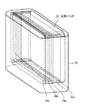
次に、図2〜4を参照して、光学素子包装体2の構成例について詳しく説明する。
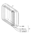
図2は、この発明の第1の実施形態による光学素子包装体の第1の構成例を示す。光学素子包装体2は、図2に示すように、例えば、支持体である拡散板23aと、光学素子である拡散フィルム24a、レンズフィルム24bおよび反射型偏光子24cと、これらを包んで一体化する包装部材22とを備える。ここでは、拡散板23aと、拡散フィルム24a、レンズフィルム24bおよび反射型偏光子24cとが光学素子積層体21を構成する。光学素子積層体21の主面は、例えば縦横比の異なる矩形状を有している。光学素子積層体21の主面とその長辺側の両端面とが帯状の包装部材22により包まれ、光学素子積層体21の短辺側の両端面が露出されている。帯状の包装部材22の長手方向の両端部同士が、例えば、光学素子積層体21の長辺側の端面にて接合される。
Next, with reference to FIGS. 2-4, the structural example of the optical element package 2 is demonstrated in detail.
FIG. 2 shows a first configuration example of the optical element package according to the first embodiment of the present invention. As shown in FIG. 2, the optical element package 2, for example, includes a diffusing
拡散板23aは、1または複数の光源の上方に設けられ、1または複数の光源11からの出射光および反射板12による反射光を拡散させて輝度を均一にするためのものである。拡散板23aとしては、例えば、光を拡散するための凹凸構造体を表面に備えるもの、拡散板23aの主構成材料とは屈折率の異なる微粒子などを含有するもの、空洞性微粒子を含有するもの、または上記凹凸構造体、微粒子および空洞性微粒子を2種以上組み合わせたものを用いることができる。微粒子としては、例えば有機フィラーおよび無機フィラーの少なくとも1種を用いることができる。また、上記凹凸構造体、微粒子および空洞性微粒子は、例えば拡散板23aの出射面に設けられる。拡散板23aの光透過率は、例えば30%以上である。
The diffusing
拡散フィルム24aは、拡散板23a上に設けられ、拡散板23aにて拡散された光を拡散などするためのものである。拡散フィルム24aとしては、例えば、光を拡散するための凹凸構造体を表面に備えるもの、拡散フィルム24aの主構成材料とは屈折率の異なる微粒子などを含有するもの、空洞性微粒子を含有するもの、または上記凹凸構造体、微粒子および空洞性微粒子を2種以上組み合わせたものを用いることができる。微粒子としては、例えば有機フィラーおよび無機フィラーの少なくとも1種を用いることができる。また、上記凹凸構造体、微粒子および空洞性微粒子は、例えば拡散フィルム24aの出射面に設けられる。
The
レンズフィルム24bは、拡散フィルム24a上に設けられ、照射光の指向性等を向上させるためのものである。レンズフィルム24bの出射面には、例えば微細なプリズムレンズ列が設けられており、このプリズムレンズの列方向の断面は、例えば略三角形状を有し、その頂点に丸みを付すことが好ましい。カットオフを改善し、広視野角を実現できるからである。
The
拡散フィルム24aおよびレンズフィルム24bは、例えば高分子材料からなり、その屈折率は例えば1.5〜1.6である。光学素子24またはそれに設けられる光学機能層を構成する材料としては、例えば、光もしくは電子線で硬化する電離性感光型樹脂、または熱により硬化する熱硬化型樹脂が好ましく、紫外線により硬化する紫外線硬化樹脂が最も好ましい。
The
反射型偏光子24cは、レンズフィルム24b上に設けられ、レンズフィルム24bにより指向性を高められた光のうち、直交する偏光成分の一方のみを通過させ、他方を反射するものである。反射型偏光子24cは、例えば有機多層膜、無機多層膜または液晶多層膜などの積層体である。また、反射型偏光子24cに異屈折率体を含有させるようにしてもよい。また、反射型偏光子24cに拡散、レンズを設けてもよい。
The
ここで、図3〜4を参照して、包装部材22の接合部の例について説明する。
図3は、包装部材の接合部の第1の例を示す。この第1の例では、図3に示すように、光学素子積層体21の端面上にて、包装部材端部の内側面と外側面とを重ね合わせるようにして接合されている。すなわち、包装部材22の端部が、光学素子積層体21の端面に倣うようにして接合されている。
Here, with reference to FIGS. 3-4, the example of the junction part of the
FIG. 3 shows a first example of the joint portion of the packaging member. In the first example, as shown in FIG. 3, the inner surface and the outer surface of the end portion of the packaging member are joined on the end surface of the
図4は、包装部材の接合部の第2の例を示す。この第2の例では、図4に示すように、光学素子積層体21の端面にて、包装部材端部の内側面同士を重ね合わせるようにして接合されている。すなわち、包装部材22の端部が、光学素子積層体21の端面から立ち上がるようにして接合されている。
FIG. 4 shows a second example of the joint portion of the packaging member. In the second example, as shown in FIG. 4, the end surfaces of the
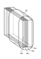
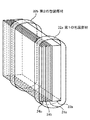
図5は、この発明の第1の実施形態による光学素子包装体の第2の構成例を示す。図5に示すように、光学素子積層体21の入射面および出射面とその短辺側の両端面とが、帯状の包装部材22により包まれ、光学素子積層体21の長辺側の両端面が露出されている。帯状の包装部材22の長手方向の端部同士が、光学素子積層体21の短辺側の端面にて接合される。
FIG. 5 shows a second configuration example of the optical element package according to the first embodiment of the present invention. As shown in FIG. 5, the entrance surface and the exit surface of the
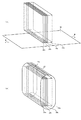
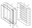
図6は、この発明の第1の実施形態による光学素子包装体の第3の構成例を示す。図6に示すように、光学素子積層体21の中央部およびその付近が帯状の包装部材22により覆われ、光学素子積層体21の短辺側の両端部が露出されている。帯状の包装部材22の長手方向の端部同士が、光学素子積層体21の長辺側の端面にて接合される。
FIG. 6 shows a third configuration example of the optical element package according to the first embodiment of the present invention. As shown in FIG. 6, the central portion of the
(1−3)光学素子包装体の製造方法
次に、上述の構成を有する光学素子包装体2の製造方法の一例について説明する。まず、図7(A)に示すように、重ね合わされた1または複数の光学素子24と支持体23とを、例えば帯状の包装部材22上に載置する。次に、図7(A)中の矢印aに示すように、例えば帯状の包装部材22の長手方向の両端部を持ち上げ、重ね合わされた1または複数の光学素子24と支持体23とを包装部材22により包む。次に、図7(B)に示すように、例えば包装部材22の長手方向の端部同士を、1または複数の光学素子24または支持体23の端面にて接合する。接合の方法としては、例えば、接着剤や溶着による接着などが挙げられる。接着剤による接着方法としては、例えばホットメルト型接着方法、熱硬化型接着方法、感圧(粘着)型接着方法、エネルギー線硬化型接着方法、水和型接着方法または吸湿・再湿型接着方法などが挙げられる。溶着による接着方法としては、例えば熱溶着、超音波溶着またはレーザ溶着などが挙げられる。その後、必要に応じて包装部材22に熱を加えることにより、包装部材22を熱収縮させるようにしてもよい。以上により、目的とする光学素子包装体2が得られる。
(1-3) Method for Manufacturing Optical Element Package Next, an example of a method for manufacturing the optical element package 2 having the above-described configuration will be described. First, as shown in FIG. 7A, the one or more
(2)第2の実施形態
この第2の実施形態は、第1の実施形態において、2種以上の大きさの光学素子24を備えるものである。2種以上の大きさの光学素子24のうち、最も小さい光学素子24が光学素子積層体21の内部に配設され、最も大きい光学素子24が光学素子積層体21の入射面側または出射面側に配設される。
(2) Second Embodiment The second embodiment includes
図8に、この発明の第2の実施形態による光学素子積層体の一構成例を示す。図8に示すように、支持体である拡散板23a上に拡散フィルム24a、レンズフィルム24bおよび反射型偏光子24cがこの順序で重ねられている。そして、この光学素子積層体21が帯状の包装部材22により包まれている。光学素子積層体21を構成する光学素子24のうちで、最も小さい拡散フィルム24が、光学素子積層体21の内部に配設され、最も大きい光学素子24の1つである反射型偏光子24cが光学素子積層体21の出射面側に配設される。
FIG. 8 shows a structural example of an optical element laminate according to the second embodiment of the present invention. As shown in FIG. 8, a
(3)第3の実施形態
この第3の実施形態では、光学素子積層体21の端面が包装部材22により覆われて光学素子積層体21が一体化され、光学素子積層体21の主面が露出されている。また、必要に応じて光学素子積層体21の主面の周縁部を包装部材22によりさらに包むようにしてもよい。
(3) Third Embodiment In the third embodiment, the end surface of the
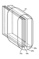
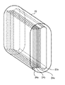
図9は、この発明の第3の実施形態による光学素子包装体の一構成例を示す。図9に示すように、光学素子積層体21の全ての端面が包装部材22により包まれて、光学素子積層体21の入射面および出射面が露出されている。
FIG. 9 shows an example of the configuration of the optical element package according to the third embodiment of the present invention. As shown in FIG. 9, all end faces of the
この発明の第3の実施形態では、光学素子包装体2の出射面が露出しているので、光学素子包装体2の出射側に配設された支持体23または光学素子24を透過した光のリタデーションを変えることなく、液晶パネル3に入射させることができる。例えば、出射側に設けられた反射型偏光子24cにより偏向分離された光をそのリタデーションを変えることなく、液晶パネル3の偏向子に入射させることができる。したがって、輝度の低下を抑制することができる。
In the third embodiment of the present invention, since the exit surface of the optical element package 2 is exposed, the light transmitted through the
(4)第4の実施形態
この第4の実施形態は、第1の実施形態において、2以上の包装部材22を備え、これらの包装部材22を互いに異なる方向から光学素子積層体21に被せて、光学素子積層体21を包んだものである。2以上の包装部材22の材料や形状はそれぞれ異なるものであってもよい。
(4) Fourth Embodiment In the fourth embodiment, in the first embodiment, two or
図10は、この発明の第4の実施形態による光学素子包装体の一構成を示す。図10に示すように、光学素子積層体21の主面は、例えば縦横比の異なる矩形状を有する。光学素子積層体21の端面が第1の包装部材31aにより包まれる。光学素子積層体21の主面およびその短辺側の端面が第2の包装部材31bにより包まれる。したがって、光学素子積層体21のすべての面が第1の包装部材31aおよび第2の包装部材31bにより包まれる。
FIG. 10 shows one configuration of the optical element package according to the fourth embodiment of the present invention. As shown in FIG. 10, the main surface of the
(5)第5の実施形態
この第5の実施形態は、第1の実施形態において、2以上の包装部材22を用いて光学素子積層体を束ねて一体化するものである。包装部材22は、例えば細長い帯状の形状を有し、光学素子積層体21の端部などを包んで光学素子積層体21を一体化する。
(5) Fifth Embodiment In the fifth embodiment, the optical element laminate is bundled and integrated using two or
図11は、この発明の第5の実施形態による光学素子包装体の一構成例を示す。図11に示すように、光学素子積層体21の主面は、例えば縦横比の異なる矩形状を有する。細長い帯状を有する第1の包装部材32aおよび第2の包装部材32bがそれぞれ、光学素子積層体21の両端部を包んで光学素子積層体21を一体化している。
FIG. 11 shows an example of the structure of an optical element package according to the fifth embodiment of the present invention. As shown in FIG. 11, the main surface of the
(6)第6の実施形態
この第6の実施形態は、第5の実施形態において、2以上の包装部材22を通すための2以上の溝または孔を備えるものである。溝または孔は、光学素子積層体21の端部近傍に設けることが好ましい。溝または孔を設けることによる光学特性の低下を抑制できるからである。
(6) Sixth Embodiment This sixth embodiment is provided with two or more grooves or holes for passing two or
図12は、この発明の第6の実施形態による光学素子積層体の一構成例を示す。図12に示すように、光学素子積層体21の主面は、例えば縦横比の異なる矩形状を有する。光学素子積層体21の長辺の両端部付近にはそれぞれ、溝21a,21aが設けられている。細長い帯状を有する第1の包装部材32aおよび第2の包装部材32bをそれぞれ、この溝21a,21aを通すようにして光学素子積層体21の両端部を包んで光学素子積層体21を一体化している。
FIG. 12 shows a structural example of an optical element laminate according to the sixth embodiment of the present invention. As shown in FIG. 12, the main surface of the
この第6の実施形態では、包装部材22を通すための溝または孔を光学素子積層体21に設けているので、製造時や輸送時における包装部材22のずれを防ぐことができる。したがって、液晶表示装置の品質や生産性を向上することができる。
In the sixth embodiment, since the
(7)第7の実施形態
第7の実施形態は、第1の実施形態において、光学素子積層体21を包装部材22により密封したものである。包装部材22の内部は、例えば常圧、低圧または真空である。包装部材22は、例えば1または複数の包装部材22からなり、その包装部材22の端辺部分が接合される。この接合部分は、光学素子積層体21の端面上に位置することが好ましい。接合部の形成による光学素子包装体2の光学特性の悪化を回避できるからである。
(7) Seventh Embodiment In the seventh embodiment, the
図13は、この発明の第7の実施形態による光学素子積層体の一構成例を示す。図13に示すように、光学素子積層体21の主面は、例えば縦横比の異なる矩形状を有し、その6方向全方位が包装部材22により包まれている。包装部材22は、例えば第1の包装部材および第2の包装部材を備え、第1の包装部材および第2の包装部材がそれぞれ、例えば光学素子積層体21の入射面および出射面を覆うようになっている。第1の包装部材と第2の包装部材とは、例えばそれらの周縁部にて接合されている。第1の包装部材と第2の包装部材とは、例えば異なる物性を有していてもよい。
FIG. 13 shows a structural example of an optical element laminate according to the seventh embodiment of the present invention. As shown in FIG. 13, the main surface of the
次に、上述の構成を有する光学素子包装体2の製造方法の一例について説明する。まず、支持体23上に1または複数の光学素子24を重ね合わせる。次に、重ね合わされた光学素子24および支持体23を第1の包装部材および第2の包装部材とにより挟み込む。次に、第1の包装部材および第2の包装部材の周縁部を接合する。以上により、目的とする光学素子包装体2が得られる。
Next, an example of a method for manufacturing the optical element package 2 having the above-described configuration will be described. First, one or more
(8)第8の実施形態
この第8の実施形態は、第7の実施形態において、包装部材22の入射面または出射面の少なくとも一方に開口を設けたものである。
(8) Eighth Embodiment In the eighth embodiment, an opening is provided on at least one of the entrance surface and the exit surface of the
図14は、この発明の第8の実施形態による光学素子包装体の一構成例を示す。図14に示すように、包装部材22の出射面には、例えば液晶パネル3の入射面と略同形状の開口22bが設けられている。また、光学素子積層体21の出射面側には、例えば反射型偏光子24cが設けられている。
FIG. 14 shows a configuration example of an optical element package according to the eighth embodiment of the present invention. As shown in FIG. 14, for example, an opening 22 b having substantially the same shape as the incident surface of the
この発明の第8の実施形態では、光学素子積層体21の出射面が露出しているので、光学素子包装体2の出射側に配設された支持体23または光学素子24を透過した光のリタデーションを変えることなく、液晶パネル3に入射させることができる。例えば、出射側に設けられた反射型偏光子24cにより偏向分離された光をそのリタデーションを変えることなく、液晶パネル3の偏向子に入射させることができる。したがって、輝度の低下を抑制することができる。
In the eighth embodiment of the present invention, since the exit surface of the
(9)第9の実施形態
この第9の実施形態は、第7の実施形態において、包装部材22に1または複数の開口を設けたものである。開口は、例えば光学素子積層体21の角部および辺部の少なくとも一方に設けられている。
(9) Ninth Embodiment In the ninth embodiment, one or more openings are provided in the
図15は、この発明の第9の実施形態による光学素子包装体の第1の構成例を示す。この第1の構成例では、図15に示すように、包装部材22は、例えば光学素子積層体21の角部21aに対応する位置に開口部22cを有する。したがって、光学素子積層体21の角部21aが包装部材22から露出されている。
FIG. 15 shows a first configuration example of an optical element package according to the ninth embodiment of the present invention. In the first configuration example, as shown in FIG. 15, the
図16は、この発明の第9の実施形態による光学素子包装体の第2の構成例を示す。この第2の構成例では、図16に示すように、包装部材22は、例えば光学素子積層体21の辺部に対応する位置に開口部22cを有する。この開口部22cは、例えばスリット状を有する。したがって、光学素子積層体21の辺部が包装部材22から露出されている。
FIG. 16 shows a second configuration example of the optical element package according to the ninth embodiment of the present invention. In this second configuration example, as shown in FIG. 16, the
この第9の実施形態では、包装部材22に開口を設け、この開口から光学素子積層体21の辺部や角部を露出させるので、光学素子包装体2の製造時や輸送時において、光学素子積層体21の辺部や角部により包装部材22が破損することを抑制できる。
In the ninth embodiment, since an opening is provided in the
(10)第10の実施形態
この第10の実施形態は、第1の実施形態において、包装部材22と、この包装部材22により包まれる支持体23および1または複数の光学素子24の少なくとも1つとを接合するものである。接合の方法としては、例えば、接着剤や溶着による接着などが挙げられる。接着剤による接着方法としては、例えばホットメルト型接着方法、熱硬化型接着方法、感圧(粘着)型接着方法、エネルギー線硬化型接着方法、水和型接着方法または吸湿・再湿型接着方法などが挙げられる。溶着による接着方法としては、例えば熱溶着、超音波溶着またはレーザ溶着などが挙げられる。
(10) Tenth Embodiment In the tenth embodiment, in the first embodiment, the
図17は、この発明の第10の実施形態による光学素子包装体の第1の構成例を示す。この第1の構成例では、接合部25が光学素子包装体2の入射面側に設けられている。この接合部25は、包装部材22の内側の面と、支持体である拡散板23aの入射面の一部または全部とが接合されて形成されている。この接合部25によって包装部材22と拡散板23aとが一体化されている。
FIG. 17 shows a first configuration example of the optical element package according to the tenth embodiment of the present invention. In the first configuration example, the
図18は、この発明の第10の実施形態による光学素子包装体の第2の構成例を示す。この第2の構成例では、接合部25が光学素子包装体2の端面に設けられている。この接合部25は、包装部材22の内側の面と、支持体である拡散板23aの端面の一部または全部とが接合されて形成されている。
FIG. 18 shows a second configuration example of the optical element package according to the tenth embodiment of the present invention. In the second configuration example, the
(11)第11の実施形態
この第11の実施形態は、第1の実施形態において、支持体23および光学素子24の少なくとも一方に凸面または凹面を設けたものである。凸面および凹面は、支持体23および光学素子24のうち、最も厚みが大きいものに設けることが好ましく、例えば透明板や拡散板などの支持体23に設けられる。支持体23および光学素子24の凸面および凹面は、例えば入射面および出射面の少なくとも一方に設けられ、凸面および凹面を組み合わせるようにしてもよい。凸面および凹面はそれぞれ、例えば縦方向(垂直方向)および横方向(水平方向)の少なくとも一方に曲率を有する凸状および凹状の曲面である。このような曲面としては、例えば放物面、円柱面、双曲面、楕円面、4次曲面および自由曲面などを挙げることができる
(11) Eleventh Embodiment In the eleventh embodiment, a convex surface or a concave surface is provided on at least one of the
図19は、この発明の第11の実施形態による光学素子包装体の第1の構成例を示す。この第1の構成例では、図19に示すように、支持体である拡散板23aの入射面が、例えば凸状の曲面となっている。この凸状の曲面は、例えば縦方向(垂直方向)に曲率を有する円柱面である。
FIG. 19 shows a first configuration example of the optical element package according to the eleventh embodiment of the present invention. In the first configuration example, as shown in FIG. 19, the incident surface of the
図20は、この発明の第11の実施形態による光学素子包装体の第2の構成例を示す。この第2の構成例では、図20に示すように、支持体である拡散板23aの入射面が、例えば凹状の曲面となっている。この凹状の曲面は、例えば縦方向(垂直方向)に曲率を有する円柱面である。
FIG. 20 shows a second configuration example of the optical element package according to the eleventh embodiment of the present invention. In the second configuration example, as shown in FIG. 20, the incident surface of the
(12)第12の実施形態
この第12の実施形態は、第1の実施形態において、支持体23および光学素子24の少なくとも一方に反りを設けたものである。この反りは、支持体23および光学素子24のうち、最も厚みが大きいものに設けることが好ましく、例えば透明板や拡散板などの支持体23に設けられる。支持体23および光学素子24の反りは、例えば入射面側または出射面側が突出するように設けられる。
(12) Twelfth Embodiment In the twelfth embodiment, in the first embodiment, at least one of the
図21は、この発明の第12の実施形態による光学素子包装体の一構成例を示す。この一構成例では、図21に示すように、支持体である拡散板23aに反りが設けられている。この反りは、例えば拡散板23aの出射面側が突出するように設けられている。拡散板23aの入射面および出射面は、例えば縦方向(垂直方向)に所定の曲率を有し、横方向(水平方向)に無限大の曲率を有している。
FIG. 21 shows a configuration example of an optical element package according to the twelfth embodiment of the present invention. In this configuration example, as shown in FIG. 21, the diffusing
(13)第13の実施形態
この第13の実施形態は、第1の実施形態において、支持体23および光学素子24の少なくとも一方の角部を曲面状または斜面状もしくはそれらを組み合わせた複合形状にしたものである。すなわち、支持体23および光学素子24の少なくとも一方の端面を曲面状または多角形状、もしくはそれらを組み合わせた複合形状にしたものである。上記形状は、支持体23および光学素子24のうち、最も厚みが大きいものに設けることが好ましく、例えば透明板や拡散板などの支持体23に設けられる。また、上記形状は、例えば、主面および端面の境界部のうち一部または全部に設けられ、好ましくは包装部材22と接触する境界部に設けられる。この境界部に設けられる曲面は例えばR面であり、境界部に設けられる斜面は例えばC面である。
(13) Thirteenth Embodiment In the thirteenth embodiment, in the first embodiment, at least one corner of the
図22は、この発明の第13の実施形態による光学素子包装体の一構成例を示す。この一構成例では、図22に示すように、支持体である拡散板23aの各面の境界部のうち、包装部材22と接触する境界部には、例えばC面などの斜面が設けられている。すなわち、拡散板23aの端部の厚さ方向断面は、例えば台形状となっている。
FIG. 22 shows a configuration example of an optical element package according to the thirteenth embodiment of the present invention. In this configuration example, as shown in FIG. 22, of the boundary portions of each surface of the
(14)第14の実施形態
この第14の実施形態は、第1の実施形態において、支持体23および光学素子24の少なくとも一方の端面にテーパを設けたものである。テーパは、支持体23および1または2以上の光学素子24のうち、入射面側および/または出射面側に配設されるものに設けることが好ましい。また、テーパは、例えば、入射面および出射面の間にある端面の一部または全部に設けられ、好ましくは包装部材22により覆われる端面に設けられる。
(14) Fourteenth Embodiment In the fourteenth embodiment, at least one end face of the
図23は、この発明の第14の実施形態による光学素子包装体の一構成例を示す。この一構成例では、図23に示すように、入射面側に配設された、支持体である拡散板23aの端面にはテーパが設けられている。このテーパは、拡散板23aの端面のうち、包装部材22により覆われる端面に設けられている。
FIG. 23 shows a structural example of an optical element package according to a fourteenth embodiment of the present invention. In this configuration example, as shown in FIG. 23, a taper is provided on an end surface of the
(15)第15の実施形態
この第15の実施形態は、第1の実施形態において、支持体23が1または複数の光学素子24を収容する収容部23bを備えるものである。この収容部23bは、支持体23の入射面および出射面の少なくとも一方に設けられる。支持体23の入射面または出射面の周縁部の一部または全部に枠部23cが設けられて、この枠部23cにより囲まれる領域が収容部23bとなる。枠部23cは、光学素子24の位置を規定できるようなものであればよく、入射面または出射面の周縁部が部分的に突き出た突起であってもよい。
(15) Fifteenth Embodiment In the fifteenth embodiment, in the first embodiment, the
図24は、この発明の第15の実施形態による光学素子包装体の一構成例を示す。図24に示すように、支持体23は、例えば支持体23の入射面および出射面の両方に光学素子24を収容する。具体的には例えば、支持体23は、入射面の収容部23bに拡散フィルム24aを収容し、出射面の収容部23bにレンズフィルム24bを収容する。支持体23の入射面および出射面は、例えば縦横比の異なる矩形状を有し、その入射面および出射面の対向する短辺または長辺に沿って枠部23cが設けられている。この枠部23cにより、光学素子24の位置が規定される。
FIG. 24 shows a structural example of an optical element package according to the fifteenth embodiment of the present invention. As shown in FIG. 24, the
(16)第16の実施形態
この第16の実施形態は、第15の実施形態において、収容部23bに収容された光学素子24の周縁部を保持する保持部をさらに設けたものである。この保持部は、支持体23の入射面および出射面の少なくとも一方に設けられる。
(16) Sixteenth Embodiment In the sixteenth embodiment, in the fifteenth embodiment, a holding portion that holds the peripheral edge of the
図25は、この発明の第16の実施形態による光学素子包装体の一構成例を示す。図25に示すように、出射面側の枠部23cには、その先端から出射面に平行で、かつ出射面の内側に向かって延びる保持部23dが設けられている。この保持部23dにより、出射側の収容部23bに収容された光学素子24の周縁部が保持される。
FIG. 25 shows a configuration example of an optical element package according to the sixteenth embodiment of the present invention. As shown in FIG. 25, the
(17)第17の実施形態
この第17の実施形態は、第1の実施形態において、1または複数の光学素子24のうちの一部または全部を光学素子包装体2の外側に設けたものである。光学素子包装体2の外側に設けられる光学素子24は、例えば、光学素子包装体2と液晶パネル3との間、および/または光学素子包装体2と照明装置1との間に配される。また、光学素子包装体2の外側に設けられた光学素子24を、例えば光学素子包装体2の出射面または入射面に接着剤などにより接合するようにしてもよい。光学素子包装体2の外側に設けられる光学素子24としては、例えば光拡散素子、光集光素子、反射型偏光子、偏光子または光分割素子などを用いることができる。
(17) Seventeenth Embodiment In the seventeenth embodiment, a part or all of one or a plurality of
図26は、この発明の第17の実施形態によるバックライトの一構成例を示す。図26に示すように、照明装置1から液晶パネル3に向かって、例えば、光学素子包装体2、光学素子である反射型偏光子24cがこの順序で設けられている。光学素子包装体2は、拡散板23a、拡散フィルム24aおよびレンズフィルム24bが包装部材22に包装されて一体化されてなるものである。
FIG. 26 shows a structural example of a backlight according to the seventeenth embodiment of the present invention. As shown in FIG. 26, for example, an optical element package 2 and a
この第17の実施形態では、反射型偏光子などの光学素子24を光学素子包装体2の外側に設けているので、反射型偏光子などの光学素子24から出射された光のリタデーションを変えることなく、液晶パネル3に入射させることができる。
In the seventeenth embodiment, since the
(18)第18の実施形態
この第18の実施形態は、第1の実施形態において、包装部材22の内側面および外側面の少なくとも一方に構造体および光学機能層を設けたものである。この光学機能層は、例えば光学素子包装体2の入射面側または出射面側の少なくとも一方に設けられる。構造体および光学機能層は、照明装置1から入射される光の特性を改善するためのものである。構造体としては、例えばシリンドリカルレンズ、プリズムレンズまたはフライアイレンズなどの各種レンズを用いることができる。また、シリンドリカルレンズやプリズムレンズなどの構造体に対してウォブルを付加してもよい。この構造体は、例えば溶融押出法または熱転写法により形成される。光学機能層としては、例えば紫外線カット機能層(UVカット機能層)または赤外線カット機能層(IRカット機能層)などを用いることができる。
(18) Eighteenth Embodiment In the eighteenth embodiment, in the first embodiment, a structure and an optical functional layer are provided on at least one of the inner surface and the outer surface of the
図27は、この発明の第18の実施形態によるバックライトの一構成例を示す。図27に示すように、照明装置1から液晶パネル3に向かって、例えば、拡散板23a、拡散フィルム24a、レンズフィルム24b、反射型偏光子24cがこの順序で設けられている。また、拡散板23aは包装部材22により包まれ、その包装部材の内側面のうち、入射側となる部分には、ムラ消し機能などを有する構造体26が設けられている。
FIG. 27 shows a configuration example of a backlight according to the eighteenth embodiment of the present invention. As shown in FIG. 27, for example, a diffusing
(19)第19の実施形態
この第19の実施形態は、第1の実施形態において、光学素子包装体2の端面の一部または全部に、光学素子包装体2の端面から出射される光を反射する反射部を設けたものである。反射部は、例えば、包装部材22の内側面および外側面、包装部材22と光学素子積層体21との間、ならびに光学素子積層体21の端面の少なくとも1つの位置に設けられている。反射部としては、例えば金属反射膜、酸化物金属膜および金属多層膜などの無機多層反射膜、高分子多層膜などの有機多層反射膜、フィラーを含有する高分子樹脂層、空孔を含有する高分子樹脂層ならびに構造反射体の少なくとも1種を用いることができ、具体的には例えば、酸化チタンなどのフィラーと気泡とを含む白色PETフィルムを用いることができる。構造反射体としては、例えば略プリズム形状の構造体を用いることができる。
(19) Nineteenth Embodiment In the nineteenth embodiment, light emitted from the end surface of the optical element package 2 is applied to a part or all of the end surface of the optical element package 2 in the first embodiment. A reflection part for reflection is provided. The reflecting portion is provided at, for example, at least one position on the inner and outer surfaces of the
図28は、この発明の第19の実施形態による光学素子包装体の第1の構成例を示す。この第1の構成例では、図28に示すように、光学素子積層体21の端面に、例えば白色PETフィルムなどの反射フィルムが配設されている。この反射フィルムは、例えば光学素子積層体21の端面に接着剤などにより接合されている。
FIG. 28 shows a first structural example of the optical element package according to the nineteenth embodiment of the present invention. In the first configuration example, as shown in FIG. 28, a reflection film such as a white PET film is disposed on the end face of the
図29は、この発明の第19の実施形態による光学素子包装体の第2の構成例を示す。この第2の構成例では、図29に示すように、光学素子積層体21の端面は反射バンド28により包まれている。反射バンド28は、例えば、帯状の反射フィルムであって、その長手方向の端部同士が接合されている。接合方法としては、例えば、第1の実施形態における包装部材22の接合方法を用いることができる。反射バンド27の基材として、例えば熱収縮性を有するものを用いることができる。
FIG. 29 shows a second configuration example of the optical element package according to the nineteenth embodiment of the present invention. In the second configuration example, as shown in FIG. 29, the end face of the
この第19の実施形態では、光学素子包装体2の端面に反射部が設けられているので、光学素子包装体2の端面にて照明装置1からの光を反射することができる。したがって、照明装置1からの光を有効に活用することができる。
In the nineteenth embodiment, since the reflecting portion is provided on the end surface of the optical element package 2, the light from the
(20)第20の実施形態
この第20の実施形態による液晶表示装置は、照明装置1としてエッジ式の照明装置を用いるものである。この照明装置は、液晶パネル3の一端側に配設された光源11からの光を導光板を介して液晶パネル全面に行き渡らせるものである。
(20) 20th Embodiment The liquid crystal display device according to the 20th embodiment uses an edge type illumination device as the
図30は、この発明の第20の実施形態による液晶表示装置の一構成例を示す。図30に示すように、この液晶表示装置は、例えば、光を出射する光学素子包装体2と、この光学素子包装体2から出射された光に基づき画像を表示する液晶パネル3とを備える。液晶パネル3としては、例えば第1の実施形態と同様のものを用いることができる。
FIG. 30 shows a configuration example of a liquid crystal display device according to the twentieth embodiment of the present invention. As shown in FIG. 30, the liquid crystal display device includes, for example, an optical element package 2 that emits light and a
光学素子包装体2は、支持体である導光板13と、導光板13の一端部に設けられた光源11と、この光源11を包むように導光板13の一端部に設けられたランプリフレクタ14と、導光板13の背後に設けられた反射シート15と、導光板13上に設けられた光学素子積層体21と、少なくとも反射シート15、導光板13および光学素子積層体21を包んでこれらの部材を一体化する包装部材22とを備える。
The optical element package 2 includes a
光学素子積層体21は、例えば1または2以上の光学素子を導光板13上に重ね合わせて構成される。具体的には例えば、光学素子積層体21は、支持体である導光板13上に、拡散シート、プリズムシート、プリズムシート、拡散シートをこの順序で重ね合わせて構成される。包装部材22としては、例えば上述の第1の実施形態と同様のものを用いることができる。
The
以上、この発明の実施形態について具体的に説明したが、この発明は、上述の実施形態に限定されるものではなく、この発明の技術的思想に基づく各種の変形が可能である。 As mentioned above, although embodiment of this invention was described concretely, this invention is not limited to the above-mentioned embodiment, The various deformation | transformation based on the technical idea of this invention is possible.
例えば、上述の実施形態において挙げた数値はあくまでも例に過ぎず、必要に応じてこれと異なる数値を用いてもよい。 For example, the numerical values given in the above embodiment are merely examples, and different numerical values may be used as necessary.
また、上述の実施形態の各構成は、この発明の主旨を逸脱しない限り、互いに組み合わせることが可能である。 The configurations of the above-described embodiments can be combined with each other without departing from the gist of the present invention.
また、上述の実施形態において、光学素子同士または光学素子と支持体とを、光学機能が損なわれないように一部を接合させてもよく、表示機能の劣化を抑える点から、端部に設けることが好ましい。 Further, in the above-described embodiment, a part of the optical elements or the optical element and the support may be joined so as not to impair the optical function, and the optical element is provided at the end from the viewpoint of suppressing the deterioration of the display function. It is preferable.
また、上述の実施形態において、光学素子包装体が、ムラ消しフィルムをさらに設けるようにしてもよい。このムラ消しフィルムは、例えば支持体の入射面と包装部材との間に設けられる。 Moreover, in the above-mentioned embodiment, the optical element packaging body may further be provided with a non-uniformity eliminating film. This unevenness eliminating film is provided, for example, between the incident surface of the support and the packaging member.
また、上述の実施形態では、包装部材としてフィルム状またはシート状のものを用いる場合を例として説明したが、包装部材としてある程度の剛性を有するケースなどを用いるようにしてもよい。 Moreover, although the case where a film-like or sheet-like one is used as the packaging member has been described as an example in the above-described embodiment, a case having a certain degree of rigidity may be used as the packaging member.
1 照明装置
2 光学素子包装体
3 液晶パネル
11 光源
12 反射板
13 導光板
14 ランプリフレクタ
15 反射シート
21 光学素子積層体
22 包装部材
23 支持体
24 光学素子
21a 溝
21b 角部
22a 接合部
22b,22c 開口
23a 拡散板
23b 収容部
23c 枠部
23d 保持部
24a 拡散フィルム
24b レンズフィルム
24c 反射型偏光子
25 接合部
26 構造体
27 反射膜
28 反射バンド
31a,32a 第1の包装部材
31b,32b 第2の包装部材
DESCRIPTION OF
Claims (11)
上記1または2以上の光学素子を支持する支持体と、
上記1または2以上の光学素子および上記支持体を包む包装部材と
を備え、
上記支持体は、
光源からの光が入射する入射面と、
上記第1の面から入射した光を上記液晶パネルに向けて出射する出射面と
を有し、
上記入射面および上記出射面の少なくとも一方の面が、凹形状または凸形状であることを特徴とする光学素子包装体。 One or more optical elements;
A support that supports the one or more optical elements;
A packaging member that wraps the one or more optical elements and the support;
The support is
An incident surface on which light from the light source is incident;
An exit surface that emits light incident from the first surface toward the liquid crystal panel;
At least one of the entrance surface and the exit surface has a concave shape or a convex shape.
上記入射面および上記出射面の少なくとも一方の周縁部に、上記光学素子を保持する保持部をさらに備えることと特徴とする請求項5記載の光学素子包装体。 The support is
6. The optical element package according to claim 5, further comprising a holding portion for holding the optical element at a peripheral portion of at least one of the entrance surface and the exit surface.
上記光源から出射された光の特性を改善し、液晶パネルに対して出射する光学素子包装体と
を備え、
上記光学素子包装体は、
1または2以上光学素子と、
上記1または2以上の光学素子を支持する支持体と、
上記1または2以上の光学素子および上記支持体を包む包装部材と
を備え、
上記支持体は、
光源からの光が入射する入射面と、
上記第1の面から入射した光を上記液晶パネルに向けて出射する出射面と
を有し、
上記入射面および上記出射面の少なくとも一方の面が、凹形状または凸形状であることを特徴とするバックライト。 A light source that emits light;
An optical element package that improves the characteristics of light emitted from the light source and emits light to the liquid crystal panel;
The optical element package is
One or more optical elements;
A support that supports the one or more optical elements;
A packaging member that wraps the one or more optical elements and the support;
The support is
An incident surface on which light from the light source is incident;
An exit surface that emits light incident from the first surface toward the liquid crystal panel;
At least one of the entrance surface and the exit surface has a concave shape or a convex shape.
上記光源から出射された光の特性を改善する光学素子包装体と、
上記光学素子包装体により特性が改善された光に基づき、画像を表示する液晶パネルと
を備え、
上記光学素子包装体は、
1または2以上光学素子と、
上記1または2以上の光学素子を支持する支持体と、
上記1または2以上の光学素子および上記支持体を包む包装部材と
を備え、
上記支持体は、
光源からの光が入射する入射面と、
上記入射面から入射した光を上記液晶パネルに向けて出射する出射面と
を有し、
上記入射面および上記出射面の少なくとも一方の面が、凹形状または凸形状であることを特徴とする液晶表示装置。 A light source that emits light;
An optical element package for improving the characteristics of light emitted from the light source;
A liquid crystal panel for displaying an image based on the light whose characteristics are improved by the optical element package,
The optical element package is
One or more optical elements;
A support that supports the one or more optical elements;
A packaging member that wraps the one or more optical elements and the support;
The support is
An incident surface on which light from the light source is incident;
An exit surface that emits light incident from the entrance surface toward the liquid crystal panel;
A liquid crystal display device, wherein at least one of the entrance surface and the exit surface is concave or convex.
上記光源から出射された光の特性を改善し、液晶パネルに対して出射する光学素子包装体と
を備え、
上記光学素子包装体は、
1または2以上光学素子と、
上記1または2以上の光学素子を支持する支持体と、
上記1または2以上の光学素子および上記支持体を包む包装部材と
を備え、
上記支持体は、
光源からの光が入射する入射面と、
上記入射面から入射した光を上記液晶パネルに向けて出射する出射面と
を有し、
上記出射面側の光学素子を支持体とすることを特徴とするバックライト。 A light source that emits light;
An optical element package that improves the characteristics of light emitted from the light source and emits light to the liquid crystal panel;
The optical element package is
One or more optical elements;
A support that supports the one or more optical elements;
A packaging member that wraps the one or more optical elements and the support;
The support is
An incident surface on which light from the light source is incident;
An exit surface that emits light incident from the entrance surface toward the liquid crystal panel;
A backlight comprising the optical element on the emission surface side as a support.
上記光源から出射された光の特性を改善する光学素子包装体と、
上記光学素子包装体により特性が改善された光に基づき、画像を表示する液晶パネルと
を備え、
上記光学素子包装体は、
1または2以上光学素子と、
上記1または2以上の光学素子を支持する支持体と、
上記1または2以上の光学素子および上記支持体を包む包装部材と
を備え、
上記支持体は、
光源からの光が入射する入射面と、
上記入射面から入射した光を上記液晶パネルに向けて出射する出射面と
を有し、
上記出射面側の光学素子を支持体とすることを特徴とする液晶表示装置。 A light source that emits light;
An optical element package for improving the characteristics of light emitted from the light source;
A liquid crystal panel for displaying an image based on the light whose characteristics are improved by the optical element package,
The optical element package is
One or more optical elements;
A support that supports the one or more optical elements;
A packaging member that wraps the one or more optical elements and the support;
The support is
An incident surface on which light from the light source is incident;
An exit surface that emits light incident from the entrance surface toward the liquid crystal panel;
A liquid crystal display device characterized in that the optical element on the exit surface side is a support.
Priority Applications (1)
| Application Number | Priority Date | Filing Date | Title |
|---|---|---|---|
| JP2007032767A JP2008197398A (en) | 2007-02-13 | 2007-02-13 | Optical element package, backlight and liquid crystal display |
Applications Claiming Priority (1)
| Application Number | Priority Date | Filing Date | Title |
|---|---|---|---|
| JP2007032767A JP2008197398A (en) | 2007-02-13 | 2007-02-13 | Optical element package, backlight and liquid crystal display |
Publications (2)
| Publication Number | Publication Date |
|---|---|
| JP2008197398A true JP2008197398A (en) | 2008-08-28 |
| JP2008197398A5 JP2008197398A5 (en) | 2010-04-08 |
Family
ID=39756396
Family Applications (1)
| Application Number | Title | Priority Date | Filing Date |
|---|---|---|---|
| JP2007032767A Pending JP2008197398A (en) | 2007-02-13 | 2007-02-13 | Optical element package, backlight and liquid crystal display |
Country Status (1)
| Country | Link |
|---|---|
| JP (1) | JP2008197398A (en) |
Cited By (3)
| Publication number | Priority date | Publication date | Assignee | Title |
|---|---|---|---|---|
| JP2010122691A (en) * | 2008-11-24 | 2010-06-03 | Samsung Electronics Co Ltd | Liquid crystal display |
| JPWO2017082387A1 (en) * | 2015-11-12 | 2018-08-02 | 富士フイルム株式会社 | Method for producing liquid crystal alignment film, method for producing three-dimensional liquid crystal cell, and three-dimensional liquid crystal cell |
| JP2018142014A (en) * | 2014-06-25 | 2018-09-13 | エルジー ディスプレイ カンパニー リミテッド | Display device |
Citations (7)
| Publication number | Priority date | Publication date | Assignee | Title |
|---|---|---|---|---|
| JP2001272509A (en) * | 2000-03-24 | 2001-10-05 | Advanced Display Inc | Light diffusion material and liquid crystal display using the same |
| JP2003242821A (en) * | 2002-02-21 | 2003-08-29 | Nichia Chem Ind Ltd | Surface light source device |
| JP2003249108A (en) * | 2002-02-25 | 2003-09-05 | Fujitsu Display Technologies Corp | Backlight apparatus, optical sheet, and liquid-crystal display device |
| JP2004233828A (en) * | 2003-01-31 | 2004-08-19 | Sanyo Electric Co Ltd | Liquid crystal display |
| JP2005250097A (en) * | 2004-03-04 | 2005-09-15 | Nitto Denko Corp | Optical member and its manufacturing method, and image display device |
| JP2005317411A (en) * | 2004-04-30 | 2005-11-10 | Sharp Corp | Backlight device |
| JP2006294356A (en) * | 2005-04-08 | 2006-10-26 | Sharp Corp | Backlight device and liquid crystal display device |
-
2007
- 2007-02-13 JP JP2007032767A patent/JP2008197398A/en active Pending
Patent Citations (7)
| Publication number | Priority date | Publication date | Assignee | Title |
|---|---|---|---|---|
| JP2001272509A (en) * | 2000-03-24 | 2001-10-05 | Advanced Display Inc | Light diffusion material and liquid crystal display using the same |
| JP2003242821A (en) * | 2002-02-21 | 2003-08-29 | Nichia Chem Ind Ltd | Surface light source device |
| JP2003249108A (en) * | 2002-02-25 | 2003-09-05 | Fujitsu Display Technologies Corp | Backlight apparatus, optical sheet, and liquid-crystal display device |
| JP2004233828A (en) * | 2003-01-31 | 2004-08-19 | Sanyo Electric Co Ltd | Liquid crystal display |
| JP2005250097A (en) * | 2004-03-04 | 2005-09-15 | Nitto Denko Corp | Optical member and its manufacturing method, and image display device |
| JP2005317411A (en) * | 2004-04-30 | 2005-11-10 | Sharp Corp | Backlight device |
| JP2006294356A (en) * | 2005-04-08 | 2006-10-26 | Sharp Corp | Backlight device and liquid crystal display device |
Cited By (4)
| Publication number | Priority date | Publication date | Assignee | Title |
|---|---|---|---|---|
| JP2010122691A (en) * | 2008-11-24 | 2010-06-03 | Samsung Electronics Co Ltd | Liquid crystal display |
| KR101493278B1 (en) | 2008-11-24 | 2015-02-16 | 삼성디스플레이 주식회사 | Liquid crystal display device and method of assembling the same |
| JP2018142014A (en) * | 2014-06-25 | 2018-09-13 | エルジー ディスプレイ カンパニー リミテッド | Display device |
| JPWO2017082387A1 (en) * | 2015-11-12 | 2018-08-02 | 富士フイルム株式会社 | Method for producing liquid crystal alignment film, method for producing three-dimensional liquid crystal cell, and three-dimensional liquid crystal cell |
Similar Documents
| Publication | Publication Date | Title |
|---|---|---|
| JP4175433B2 (en) | Optical element package, backlight, and liquid crystal display device | |
| JP4175431B1 (en) | Optical element package, backlight, and liquid crystal display device | |
| JP4148299B1 (en) | Optical package and manufacturing method thereof, lighting device, and display device | |
| WO2010032882A1 (en) | Optical element laminate, and manufacturing method therefor, backlight and liquid crystal display device | |
| JP2009300801A (en) | Optical package, manufacturing method thereof, backlight, and liquid crystal display device | |
| JP2009076405A (en) | Optical element packing body, back light and liquid crystal display | |
| JP4135118B1 (en) | Liquid crystal display | |
| JP4251225B2 (en) | Optical element package, backlight and liquid crystal display device | |
| JP2008250327A (en) | Package, manufacturing method thereof, backlight, and liquid crystal display | |
| JP2008197398A (en) | Optical element package, backlight and liquid crystal display | |
| JP2010535359A (en) | Light management assembly | |
| JP2008261961A (en) | Optical element package, backlight and liquid crystal display | |
| JP2008261962A (en) | Optical element wrapped body, backlight, and liquid crystal display | |
| JP2010044221A (en) | Optical package, lighting system, and display device | |
| JP2010044219A (en) | Optical package, method for manufacturing the same, backlight, and liquid crystal display | |
| JP2009075573A (en) | Optical element package, backlight, and liquid crystal display device | |
| JP2010044953A (en) | Optical packing body, manufacturing method thereof, backlight, and liquid crystal display device | |
| JP2009075545A (en) | Optical element packaging body, backlight and liquid crystal display device provided with the same and manufacturing method of optical element packaging body | |
| JP5163516B2 (en) | Optical element package, backlight and liquid crystal display device | |
| JP2010042839A (en) | Optical package, illumination device, and display | |
| JP2008261959A (en) | Optical element wrapped body, backlight, and liquid crystal display | |
| JP2010044952A (en) | Optical packing body, lighting device, and display device | |
| JP2009300791A (en) | Optical package, lighting device, and display device | |
| JP2009093148A (en) | Optical package, method for manufacturing the same, illuminator and display | |
| JP2009300800A (en) | Optical element package body, its manufacturing method, backlight, and liquid crystal display device |
Legal Events
| Date | Code | Title | Description |
|---|---|---|---|
| A621 | Written request for application examination |
Free format text: JAPANESE INTERMEDIATE CODE: A621 Effective date: 20100201 |
|
| A521 | Written amendment |
Free format text: JAPANESE INTERMEDIATE CODE: A523 Effective date: 20100224 |
|
| A977 | Report on retrieval |
Free format text: JAPANESE INTERMEDIATE CODE: A971007 Effective date: 20120216 |
|
| A131 | Notification of reasons for refusal |
Free format text: JAPANESE INTERMEDIATE CODE: A131 Effective date: 20120828 |
|
| A02 | Decision of refusal |
Free format text: JAPANESE INTERMEDIATE CODE: A02 Effective date: 20121218 |