JP2008166320A - Inspection device - Google Patents
Inspection device Download PDFInfo
- Publication number
- JP2008166320A JP2008166320A JP2006350814A JP2006350814A JP2008166320A JP 2008166320 A JP2008166320 A JP 2008166320A JP 2006350814 A JP2006350814 A JP 2006350814A JP 2006350814 A JP2006350814 A JP 2006350814A JP 2008166320 A JP2008166320 A JP 2008166320A
- Authority
- JP
- Japan
- Prior art keywords
- mark
- wafer
- stage
- correction
- coordinates
- Prior art date
- Legal status (The legal status is an assumption and is not a legal conclusion. Google has not performed a legal analysis and makes no representation as to the accuracy of the status listed.)
- Granted
Links
Images

Landscapes
- Testing Or Measuring Of Semiconductors Or The Like (AREA)
- Container, Conveyance, Adherence, Positioning, Of Wafer (AREA)
Abstract
【課題】
ウェハの位置合せにおいて、パターンサーチによるマークの誤認識を防止し、位置合せの精度を保持してスループットを向上する。
【解決手段】
第1及び第2のマークを検出する手段と、第1及び第2のマークの座標からウェハの補正角を算出する手段と、ウェアの補正角と第1または第2の座標から第3のマークの座標を算出する手段と、算出した第3のマークの座標をステージが補正角回転したときの座標を算出する手段と、第3のマークを算出する手段を備え、算出した第3の座標と検出した第3の座標を比較して位置合せを行う。
【選択図】図1【Task】
In wafer alignment, erroneous mark recognition by pattern search is prevented, and alignment accuracy is maintained and throughput is improved.
[Solution]
Means for detecting the first and second marks; means for calculating a wafer correction angle from the coordinates of the first and second marks; and a third mark from the wear correction angle and the first or second coordinates. Means for calculating the coordinates of the third mark, means for calculating the coordinates of the calculated third mark when the stage rotates the correction angle, means for calculating the third mark, and the means for calculating the third mark, The detected third coordinates are compared to perform alignment.
[Selection] Figure 1
Description
本発明はパターンウェハを検査する検査装置において、特に可動ステージ上に置かれたパターンウェハの位置ずれを自動的に整列を行う検査装置に関する。 The present invention relates to an inspection apparatus for inspecting a pattern wafer, and more particularly to an inspection apparatus for automatically aligning a positional deviation of a pattern wafer placed on a movable stage.
パターンウェハは正確,精密に整列されたチップが並べられている。パターンウェハの検査ではウェハがステージのX,Y方向に対して整列した状態で置かれている必要がある。しかし、ウェハがステージに搬送された直後ではX,Y方向に対して整列された状態になっておらず、ステージを回転させてX,Y方向に整列させる位置合せが必要である。 Pattern wafers are arranged with chips that are precisely and precisely aligned. In the inspection of the pattern wafer, the wafer needs to be placed in an aligned state with respect to the X and Y directions of the stage. However, immediately after the wafer is transferred to the stage, the wafer is not aligned in the X and Y directions, and alignment is required to rotate the stage and align it in the X and Y directions.
パターンウェハの位置合せにおいて、複数の補正用マークを用い、それらの位置をCCDカメラ等で撮像し、パターンマッチング処理により位置を計測し、複数点数から補正するためのステージの回転角度を求める。 In the alignment of the pattern wafer, a plurality of correction marks are used, their positions are picked up by a CCD camera or the like, the position is measured by pattern matching processing, and the rotation angle of the stage for correction from a plurality of points is obtained.
一般的に位置合せにおいて2種類の倍率カメラを用いて撮像する。算出する補正角の精度を上げるには補正用マークの位置を高い精度で検出する必要がある。このためには高倍率のカメラで撮像する必要がある。しかし、高倍率カメラの撮像視野は狭く、補正用マークを一度の撮像で捉える確率は低くなる。このため低倍率カメラで大枠の位置を検出し、高倍率カメラに切替えて精度を高める方式を行っている。 In general, imaging is performed using two types of magnification cameras in alignment. In order to increase the accuracy of the calculated correction angle, it is necessary to detect the position of the correction mark with high accuracy. For this purpose, it is necessary to capture images with a high-magnification camera. However, the imaging field of view of the high-magnification camera is narrow, and the probability of capturing the correction mark with a single imaging is low. For this reason, a method of detecting the position of the large frame with a low magnification camera and switching to a high magnification camera to increase accuracy is performed.
ただし、この方式では位置合せに時間がかかってしまう課題がある。このため、検査スループットを向上させるために位置合せ精度と搬送時のステージの位置ズレから最適な倍率を導き出し、単倍率で位置合せを行うことが考えられる。関連する文献として、下記特許文献1がある。 However, this method has a problem that it takes time for alignment. For this reason, in order to improve the inspection throughput, it is conceivable to derive an optimum magnification from the alignment accuracy and the positional deviation of the stage during conveyance and perform alignment at a single magnification. As related documents, there is the following Patent Document 1.
しかしながら、単倍率では他の模様を補正用マークと誤認識してしまったことを検知するために補正角を算出するための補正用マークと位置合せの精度を確認するための確認用マークの3点以上が必要になる。確認用の補正用マークの座標位置が正しい位置に配置されたことで位置合せの精度を確認するが、ウェハをステージに搬送したときにウェハの中心とステージの中心がずれてしまい、確認用の補正用マークの座標位置もずれており、補正前に確認用マークの座標位置を検出しておく必要があるが、ステージの移動とパターンマッチングの処理が必要となり、時間が掛かってしまう。このために検出した補正用マークの座標から確認用マークの座標を算出しておく必要がある。 However, at a single magnification, there are three correction marks for calculating a correction angle and a confirmation mark for confirming the alignment accuracy in order to detect that another pattern is erroneously recognized as a correction mark. More points are needed. The accuracy of alignment is confirmed by the coordinate position of the correction mark for confirmation being placed at the correct position. However, when the wafer is transported to the stage, the center of the wafer and the center of the stage are misaligned. The coordinate position of the correction mark is also shifted, and it is necessary to detect the coordinate position of the confirmation mark before correction. However, it takes time to move the stage and perform pattern matching. Therefore, it is necessary to calculate the coordinates of the confirmation mark from the detected coordinates of the correction mark.
本発明の一つの目的は、検査装置の検査スループットを向上することにある。 One object of the present invention is to improve the inspection throughput of an inspection apparatus.
上記目的を達成するための本発明の一つの特徴は、補正用の2点のマークの座標を検出する手段と、該補正用の2点のマークの座標からウェハの補正角を計算する手段と、ウェハの補正角と補正用マークの座標と予め登録されている確認用マークの座標からウェハがステージに搬送されたときの確認用マークの座標を算出する手段と、ステージを補正角回転させたときの確認用マークの座標を算出する手段と、確認用マークの座標を検出する手段と、検出した確認用マークの座標とステージが回転したときの算出した確認用マークの座標を比較する手段を具備することにある。本発明の前記特徴その他の特徴は、以下の記載により更に説明される。 One feature of the present invention for achieving the above object is that means for detecting the coordinates of two correction marks and means for calculating the correction angle of the wafer from the coordinates of the two correction marks. The means for calculating the coordinates of the confirmation mark when the wafer is transported to the stage from the correction angle of the wafer, the coordinates of the correction mark and the coordinates of the confirmation mark registered in advance, and the stage is rotated by the correction angle Means for calculating the coordinates of the confirmation mark at the time, means for detecting the coordinates of the confirmation mark, means for comparing the coordinates of the detected confirmation mark with the coordinates of the confirmation mark calculated when the stage rotates It is to have. The above and other features of the present invention will be further explained by the following description.
本発明によれば、検査装置の検査スループットを向上できる。例えば、位置合せを行う場合、2点の座標からウェハの傾きを計算するが、補正を行った後に補正精度を確認する必要があり、確認のために2点の座標を検出するには時間がかかるため、他の1点の座標を検出することで確認を行うと時間が短くて済むが、ウェハの搬送後にステージとウェハの中心がずれてしまい、確認用のマークの位置もずれているため確認用のマークの座標を検出することが必要になるが、ステージとウェハの中心のずれを加味して確認用のマークの位置を算出することで補正前に確認用のマークを検出する必要がなく、位置合せを行うことができる。 According to the present invention, the inspection throughput of the inspection apparatus can be improved. For example, when alignment is performed, the tilt of the wafer is calculated from the coordinates of two points. However, it is necessary to check the correction accuracy after correction, and it takes time to detect the coordinates of the two points for confirmation. For this reason, if the confirmation is performed by detecting the coordinates of another point, the time can be shortened. However, the stage and the center of the wafer are displaced after the wafer is transferred, and the position of the confirmation mark is also displaced. It is necessary to detect the coordinates of the confirmation mark, but it is necessary to detect the confirmation mark before correction by calculating the position of the confirmation mark taking into account the deviation between the center of the stage and the wafer. And alignment can be performed.
位置合せの処理を高速にし、マークの誤認識を検出することを、2点の補正用マークと1点の確認用マークによる位置合せにより実現した本発明の実施形態を以下説明する。 An embodiment of the present invention that realizes high-speed alignment processing and detection of erroneous mark recognition by alignment using two correction marks and one confirmation mark will be described below.
本発明に係る対象物の検査装置の実施の形態を説明する。図1は本発明の一実施例に係る検査装置の構成を示す。同図において10はウェハ19を移動及び回転させるステージ、11はウェハ19の表面を照射するための光学装置、12は光学装置11で照らしたウェハ19の表面を撮影するためのカメラ、13はカメラ12で撮像したウェハ19の表面の画像を取り込むためのキャプチャーボード、14はキャプチャーボード13で取り込んだ画像データ、15は画像データ14を処理するために置いておく主記憶、16は画像データ14を処理するための画像処理演算器、17はステージ10を制御するステージ制御ソフトを有するステージ制御演算器、18はステージ10を制御するステージ制御器、
19はウェハを構成している。
An embodiment of an object inspection apparatus according to the present invention will be described. FIG. 1 shows the configuration of an inspection apparatus according to an embodiment of the present invention. In the figure, 10 is a stage for moving and rotating the
図2は本発明の一実施例に係るウェハ3上に形成される補正用マークの配置を示す。
101は補正用マーク1、102は補正用マーク2、103は確認用マーク3である。確認用マーク3は補正用マーク2と近傍にあれば、どの位置にあっても構わない。
FIG. 2 shows the arrangement of correction marks formed on the wafer 3 according to an embodiment of the present invention.
101 is a
図3はウェハ3がステージ10に搬送されてから位置合せを行うまでの動きを示している。209はウェハ19がステージ10に搬送された直後のウェハの位置、200はステージ10の回転中心、201はウェハ19が209の位置にあるときのウェハ中心、203,204及び205はウェハ19が209の位置にあるときの補正用マーク1、補正用マーク2及び補正用マーク3のそれぞれの座標位置、210は位置合せを行った後のウェハ19の位置、206,207及び208はウェハ19が210の位置にあるときの補正用マーク1,補正用マーク2及び補正用マーク3の座標位置である。
FIG. 3 shows the movement from the transfer of the wafer 3 to the
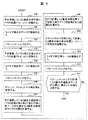
図4は該検査装置での位置合せ処理のフローを示す。 FIG. 4 shows a flow of alignment processing in the inspection apparatus.
ステップ300では予め登録されている補正用マーク101の座標位置P1(x1,
y1)にステージ10を移動する。ステップ301ではカメラ12により補正用マーク1の撮像を行う。ステップ302では撮像した画像に対してパターンマッチングを行い、補正用マーク203の座標位置を検出する。このとき、ウェハ19はステージ10に搬送された状態で209の位置にあり、補正用マーク1は203の座標位置にある。ステップ
302では検出した203の座標位置を取得後、ステップ303によって予め登録している補正用マーク2の座標位置にステージ10を移動する。このとき、ウェハ19はステージ10に搬送された状態で209の位置にあり、補正用マーク2は204の座標位置にある。ステップ304によってカメラ12により補正用マーク2の撮像を行う。ステップ
305では撮像した画像に対してパターンマッチングを行い、補正用マーク2の座標位置を検出する。ステップ306ではステップ302,305から検出した補正用マーク1及び補正用マーク2の座標203及び204から補正角を計算する。ステップ307ではステップ306で計算した補正角とステップ302で算出した1番目の補正用マークの座標と予め登録した3番目の確認用マークの座標から位置補正を行う前の3番目の座標を求める。308ではステップ307で算出した3番目の確認用マークの座標に対してステージ10を補正角回転させたときの座標位置を計算する。ステップ309では該ステージ10をステップ306から算出した補正角回転させ、ステップ309で算出した座標位置にステージ10を移動させる。ステップ310ではカメラ12により確認用マーク3の撮像を行う。ステップ311ではパターンマッチングにより確認用マーク3の座標208を検出する。ステップ312ではステップ308で計算した補正用マーク3の座標位置208とステップ311で計測した補正用マーク3の座標位置208の差分を行う。差分値が予め登録された閾値以内であれば位置補正は終了する。もし、閾値よりも大きい場合、ステップ303から処理を繰返す。本発明の実施形態は、上記に限定されるものではなく、その技術思想の範囲内で変形可能である。
In
The
10 ステージ
11 光学装置
12 カメラ
13 キャプチャーボード
14 画像データ
15 主記憶
16 画像処理演算器
17 ステージ制御演算器
18 ステージ制御器
19 ウェハ
DESCRIPTION OF
Claims (3)
第1のマークはウェハ端の近傍に位置し、該ステージにより第1のマークの位置に移動し、該マークの位置を検出する手段と、
第2のマークは第1のマークとXまたはY方向に相対的な位置に位置し、該ステージにより第2のマークに移動して該マークの位置を検出する手段と、
第1及び第2のマークの位置からウェハの補正角を算出する手段と、
第3のマークは第1及び第2のマークと同一線上にあって、第2のマークの近傍に位置し、検出した第1または第2のマークの位置とウェハの補正角と予め登録した第3のマークの位置から第3のマークの位置を算出する手段と、
ステージを補正角回転したときの第3のマークの位置を算出する手段と、
該ウェハの補正角に対して該ステージを回転して補正する手段と、
該ウェハを補正後、該ステージにより第3のマークに移動して該マークの位置を検出する手段と、
を備えることを特徴とする検査装置。 An inspection apparatus for holding a wafer and aligning the wafer with a stage that can move and rotate in the X and Y directions,
Means for detecting the position of the first mark located near the wafer edge, moved to the position of the first mark by the stage;
Means for detecting the position of the mark by moving the second mark to the second mark by the stage, relative to the first mark in the X or Y direction;
Means for calculating a correction angle of the wafer from the positions of the first and second marks;
The third mark is on the same line as the first and second marks and is located in the vicinity of the second mark. The detected first or second mark position, the wafer correction angle, and the previously registered first mark are registered in advance. Means for calculating the position of the third mark from the position of the third mark;
Means for calculating the position of the third mark when the stage is rotated by a correction angle;
Means for rotating and correcting the stage with respect to the correction angle of the wafer;
Means for detecting the position of the mark by moving to the third mark by the stage after correcting the wafer;
An inspection apparatus comprising:
を備えることを特徴とする検査装置。 The means according to claim 1, wherein the position calculated by the means for calculating the position of the third mark is compared with the position detected by the means for detecting the position of the third mark;
An inspection apparatus comprising:
検出した第3と第4のマークの座標から補正角を算出する手段と、
第3または第4のマークの座標と該補正角から第1のマークを算出する手段と、
該ウェハの補正角に対して該ステージを回転して補正する手段と、
該ウェハを補正後、該ステージにより第1のマークに移動して該マークの位置を検出する手段と、
を備えることを特徴とする検査装置。 The means for comparing the calculated third mark with the detected third mark according to claim 2, wherein the fourth mark is located in the vicinity of the first mark when the third mark is more than a specific distance, Means for detecting the position by moving to the fourth mark by the stage;
Means for calculating a correction angle from the coordinates of the detected third and fourth marks;
Means for calculating the first mark from the coordinates of the third or fourth mark and the correction angle;
Means for rotating and correcting the stage with respect to the correction angle of the wafer;
Means for detecting the position of the mark by moving to the first mark by the stage after correcting the wafer;
An inspection apparatus comprising:
Priority Applications (3)
| Application Number | Priority Date | Filing Date | Title |
|---|---|---|---|
| JP2006350814A JP4902342B2 (en) | 2006-12-27 | 2006-12-27 | Inspection device |
| US12/003,123 US7898653B2 (en) | 2006-12-20 | 2007-12-20 | Foreign matter inspection apparatus |
| US13/009,366 US8395766B2 (en) | 2006-12-20 | 2011-01-19 | Foreign matter inspection apparatus |
Applications Claiming Priority (1)
| Application Number | Priority Date | Filing Date | Title |
|---|---|---|---|
| JP2006350814A JP4902342B2 (en) | 2006-12-27 | 2006-12-27 | Inspection device |
Publications (2)
| Publication Number | Publication Date |
|---|---|
| JP2008166320A true JP2008166320A (en) | 2008-07-17 |
| JP4902342B2 JP4902342B2 (en) | 2012-03-21 |
Family
ID=39695456
Family Applications (1)
| Application Number | Title | Priority Date | Filing Date |
|---|---|---|---|
| JP2006350814A Expired - Fee Related JP4902342B2 (en) | 2006-12-20 | 2006-12-27 | Inspection device |
Country Status (1)
| Country | Link |
|---|---|
| JP (1) | JP4902342B2 (en) |
Cited By (1)
| Publication number | Priority date | Publication date | Assignee | Title |
|---|---|---|---|---|
| US9851548B2 (en) | 2011-08-23 | 2017-12-26 | Hitachi High-Technologies Corporation | Optical microscope device and testing apparatus comprising same |
Citations (2)
| Publication number | Priority date | Publication date | Assignee | Title |
|---|---|---|---|---|
| JPH1197511A (en) * | 1997-09-18 | 1999-04-09 | Canon Inc | Alignment apparatus and method |
| JPH11220006A (en) * | 1998-01-29 | 1999-08-10 | Techno Horon:Kk | Method for alignment of object |
-
2006
- 2006-12-27 JP JP2006350814A patent/JP4902342B2/en not_active Expired - Fee Related
Patent Citations (2)
| Publication number | Priority date | Publication date | Assignee | Title |
|---|---|---|---|---|
| JPH1197511A (en) * | 1997-09-18 | 1999-04-09 | Canon Inc | Alignment apparatus and method |
| JPH11220006A (en) * | 1998-01-29 | 1999-08-10 | Techno Horon:Kk | Method for alignment of object |
Cited By (1)
| Publication number | Priority date | Publication date | Assignee | Title |
|---|---|---|---|---|
| US9851548B2 (en) | 2011-08-23 | 2017-12-26 | Hitachi High-Technologies Corporation | Optical microscope device and testing apparatus comprising same |
Also Published As
| Publication number | Publication date |
|---|---|
| JP4902342B2 (en) | 2012-03-21 |
Similar Documents
| Publication | Publication Date | Title |
|---|---|---|
| CN104779191B (en) | Mark detection method | |
| CN114695225A (en) | Wafer pre-alignment device and wafer pre-alignment method | |
| US20030164876A1 (en) | Procedure and device for measuring positions of continuous sheets | |
| JP6208419B2 (en) | Calculation device, transfer robot system, and calculation method | |
| JP5057489B2 (en) | Alignment apparatus and alignment method | |
| CN103079746A (en) | Laser processing apparatus and substrate position detecting method | |
| JP2004288792A (en) | Alignment device and alignment method | |
| JP2008128651A (en) | Pattern alignment method, and pattern inspecting device and system | |
| JP2008036918A (en) | Screen printing apparatus and image recognition alignment method | |
| KR20180136771A (en) | Apparatus for aligning semiconductor wafer and method thereof | |
| CN112213328A (en) | Wafer inspection apparatus | |
| WO2015145864A1 (en) | Position displacement detection method, position displacement detection device, drawing device, and substrate inspection device | |
| TWI910424B (en) | Apparatus and method for pre-aligning fiducial located on substrate to predetermined location on substrate holder and relevant computer-readable medium | |
| JP2010021411A (en) | Device and method for positioning workpiece | |
| CN1935480A (en) | Partition device and alignment method for wafer | |
| JP4385699B2 (en) | Semiconductor wafer direction adjusting method and semiconductor wafer direction adjusting apparatus | |
| JP4902342B2 (en) | Inspection device | |
| CN110744920B (en) | Method and system for positioning printed product | |
| JP6784151B2 (en) | Plate-shaped body processing method and plate-shaped body processing equipment | |
| JP2008014700A (en) | Workpiece inspection method and workpiece inspection device | |
| JP2015040698A (en) | Alignment device and inspection device | |
| JP6177075B2 (en) | Processing method | |
| JP2000199704A (en) | Calibration method for image processing device | |
| JP5398314B2 (en) | Exposure apparatus and exposure method | |
| JP5602548B2 (en) | Machining position detection method |
Legal Events
| Date | Code | Title | Description |
|---|---|---|---|
| A621 | Written request for application examination |
Free format text: JAPANESE INTERMEDIATE CODE: A621 Effective date: 20090204 |
|
| A521 | Written amendment |
Free format text: JAPANESE INTERMEDIATE CODE: A523 Effective date: 20090204 |
|
| A131 | Notification of reasons for refusal |
Free format text: JAPANESE INTERMEDIATE CODE: A131 Effective date: 20100928 |
|
| A977 | Report on retrieval |
Free format text: JAPANESE INTERMEDIATE CODE: A971007 Effective date: 20100930 |
|
| A521 | Written amendment |
Free format text: JAPANESE INTERMEDIATE CODE: A523 Effective date: 20101125 |
|
| A131 | Notification of reasons for refusal |
Free format text: JAPANESE INTERMEDIATE CODE: A131 Effective date: 20110405 |
|
| A521 | Written amendment |
Free format text: JAPANESE INTERMEDIATE CODE: A523 Effective date: 20110624 |
|
| TRDD | Decision of grant or rejection written | ||
| A01 | Written decision to grant a patent or to grant a registration (utility model) |
Free format text: JAPANESE INTERMEDIATE CODE: A01 Effective date: 20111206 |
|
| A01 | Written decision to grant a patent or to grant a registration (utility model) |
Free format text: JAPANESE INTERMEDIATE CODE: A01 |
|
| A61 | First payment of annual fees (during grant procedure) |
Free format text: JAPANESE INTERMEDIATE CODE: A61 Effective date: 20111228 |
|
| R150 | Certificate of patent or registration of utility model |
Free format text: JAPANESE INTERMEDIATE CODE: R150 |
|
| FPAY | Renewal fee payment (event date is renewal date of database) |
Free format text: PAYMENT UNTIL: 20150113 Year of fee payment: 3 |
|
| LAPS | Cancellation because of no payment of annual fees |