JP2008160661A - Amplifier protection circuit - Google Patents
Amplifier protection circuit Download PDFInfo
- Publication number
- JP2008160661A JP2008160661A JP2006349345A JP2006349345A JP2008160661A JP 2008160661 A JP2008160661 A JP 2008160661A JP 2006349345 A JP2006349345 A JP 2006349345A JP 2006349345 A JP2006349345 A JP 2006349345A JP 2008160661 A JP2008160661 A JP 2008160661A
- Authority
- JP
- Japan
- Prior art keywords
- circuit
- potential
- bias
- amplifier
- state
- Prior art date
- Legal status (The legal status is an assumption and is not a legal conclusion. Google has not performed a legal analysis and makes no representation as to the accuracy of the status listed.)
- Pending
Links
- 238000001514 detection method Methods 0.000 claims abstract description 53
- 238000005513 bias potential Methods 0.000 claims abstract description 18
- 238000010586 diagram Methods 0.000 description 8
- 239000003990 capacitor Substances 0.000 description 4
- 230000008878 coupling Effects 0.000 description 4
- 238000010168 coupling process Methods 0.000 description 4
- 238000005859 coupling reaction Methods 0.000 description 4
- 230000002159 abnormal effect Effects 0.000 description 1
- 230000002411 adverse Effects 0.000 description 1
- 230000003321 amplification Effects 0.000 description 1
- 238000012544 monitoring process Methods 0.000 description 1
- 238000003199 nucleic acid amplification method Methods 0.000 description 1
Images

Landscapes
- Amplifiers (AREA)
Abstract
【課題】BTL増幅器の保護回路の条件設定が難しい。
【解決手段】BTL増幅器2の非反転出力端子NOUT+の電位VOUT+及び反転出力端子NOUT−の電位VOUT−に基づいて、NOUT+又はNOUT−が電源VCC等に短絡した誤接続状態を検出する。VOUT+及びVOUT−の間を抵抗分割し、それらの中点の電位V1を生成する。正常状態では、V1はVOUT+及びVOUT−の基準バイアス電位Vb0に保たれる。バランス判定回路14は、V1がVb0近傍にあるときLレベルを出力し、V1が当該近傍からはずれたときHレベルを出力する。範囲外状態検出回路6は、VOUT+又はVOUT−が、Vb0を内包する許容バイアス範囲から外れるとHレベルを出力する。AND回路8が、バランス判定回路14と範囲外状態検出回路6との両方がH出力状態であることを検出すると、制御回路10はバイアス回路12をオフしてBTL増幅器2を保護する。
【選択図】図1
It is difficult to set conditions for a protection circuit of a BTL amplifier.
A based on the BTL amplifier 2 of the non-inverting output terminal N OUT + of the potential V OUT + and the inverted output terminal N OUT- potential V OUT-, N OUT + or N OUT- is connected incorrectly shorted to a power supply V CC, etc. Detect state. A resistance is divided between V OUT + and V OUT− to generate a potential V 1 at the midpoint thereof. In a normal state, V 1 is kept at the reference bias potential V b0 of V OUT + and V OUT− . Balance determination circuit 14, V 1 outputs the L level when it is in the vicinity of V b0, V 1 outputs an H level when off the said vicinity. The out-of-range state detection circuit 6 outputs an H level when V OUT + or V OUT− is out of the allowable bias range including V b0 . When the AND circuit 8 detects that both the balance determination circuit 14 and the out-of-range state detection circuit 6 are in the H output state, the control circuit 10 turns off the bias circuit 12 to protect the BTL amplifier 2.
[Selection] Figure 1
Description
本発明は、BTL(Balanced Transformer Less)増幅器を保護する保護回路に関する。 The present invention relates to a protection circuit for protecting a BTL (Balanced Transformer Less) amplifier.
BTL増幅器は、逆位相の2つのSEPP(Single Ended Push-Pull)回路を含み、これら2つのSEPP回路の出力端子から直流電位が等しく逆位相の出力信号を出力する。BTL増幅器は、これら直流電位がバランスした2つの出力端子間に負荷を接続することで、負荷に流れる直流電流をカットするための結合コンデンサを必要としない。結合コンデンサを必要とする増幅器では、信号が低周波になる程、大きな結合コンデンサを必要とし、このことが設計を困難とする。これに対して、BTL増幅器は、結合コンデンサが不要であるため、超低周波増幅器や直流増幅器の出力段に使われる。 The BTL amplifier includes two anti-phase SEPP (Single Ended Push-Pull) circuits, and outputs an output signal having the same DC potential and opposite phase from the output terminals of these two SEPP circuits. The BTL amplifier does not require a coupling capacitor for cutting the direct current flowing through the load by connecting the load between the two output terminals in which the direct current potential is balanced. In an amplifier that requires a coupling capacitor, the lower the frequency of the signal, the larger the coupling capacitor required, which makes design difficult. On the other hand, since the BTL amplifier does not require a coupling capacitor, it is used for an output stage of an ultra-low frequency amplifier or a DC amplifier.
ここで、BTL増幅器の各出力端子が、正電源VCCや接地電位GND等と短絡すると、SEPP回路を構成する出力トランジスタに過大な電流が流れる等の不都合が生じる。そこで、このような短絡からBTL増幅器を保護する保護回路が必要となる。 Here, when each output terminal of the BTL amplifier is short-circuited with the positive power supply VCC , the ground potential GND, or the like, inconveniences such as excessive current flowing in the output transistor constituting the SEPP circuit occur. Therefore, a protection circuit that protects the BTL amplifier from such a short circuit is required.
図4は、従来の保護回路を説明するための回路図であり、BTL増幅器を構成する1つのSEPP回路の出力段の構成を示している。図4に示すSEPP回路は、出力トランジスタQ01及びQ02を備え、Q01はコレクタ及びエミッタをそれぞれVCC及び出力端子NOUTに接続され、Q02はコレクタ及びエミッタをそれぞれNOUT及びGNDに接続される。Q01のベースとNOUTとの間の電圧がR01とR02とで抵抗分割され検出トランジスタQ03のベースに入力される。また、Q02のベースとGNDとの間の電圧がR03とR04とで抵抗分割され検出トランジスタQ04のベースに入力される。例えば、NOUTとVCCとが短絡した場合(この場合を以下、天絡と称する。)、Q02に大きなコレクタ電流IC2が流れ、Q02のベース-エミッタ間電圧VBEは、VBE-IC特性に基づいて増加する。このVBEの増加はQ04の導通状態を変化させる。一方、NOUTとGNDとが短絡した場合(この場合を以下、地絡と称する。)、Q01のコレクタ電流IC1が大電流となることに応じてVBEが変化し、Q03の導通状態を変化させる。 FIG. 4 is a circuit diagram for explaining a conventional protection circuit, and shows a configuration of an output stage of one SEPP circuit constituting a BTL amplifier. SEPP circuit shown in FIG. 4, an output transistor Q01 and Q02, Q01 are connected the collector and the emitter to V CC and the output terminal N OUT, respectively, Q02 are connected the collector and emitter N OUT and GND, respectively. Voltage between the base and N OUT of Q01 is inputted to the resistor divided based detection transistor Q03 with R01 and R02. Further, the voltage between the base of Q02 and GND is resistance-divided by R03 and R04 and input to the base of the detection transistor Q04. For example, when N OUT and V CC are short-circuited (this case is hereinafter referred to as a power fault), a large collector current I C2 flows in Q02, and the base-emitter voltage V BE of Q02 is V BE -I. It increases based on the C characteristic. This increase in V BE changes the conduction state of Q04. On the other hand, when N OUT and GND are short-circuited (this case is hereinafter referred to as a ground fault), V BE changes in response to the collector current I C1 of Q01 becoming a large current, and the conduction state of Q03 is changed. Change.
従来は、BTL増幅器の反転出力端子NOUT−、非反転出力端子NOUT+それぞれに、図4に示す構成のSEPP回路を設ける。保護回路の動作を制御する制御回路は、それらSEPP回路における出力トランジスタQ01,Q02の短絡時大電流を検出トランジスタQ03,Q04のコレクタ電流IC3,IC4の変化に基づいて検出し、天絡又は地絡という誤接続状態であることを判定する。そして、制御回路は、誤接続状態と判定すると、BTL増幅器にバイアス電源を供給するバイアス回路をオフして、BTL増幅器の動作を停止させる。
検出トランジスタQ03,Q04に流れるIC3,IC4を検出電流として、出力トランジスタQ01,Q02のVBEの変化を検出する従来の構成は、R01とR02との抵抗比及びR03とR04との抵抗比を、誤接続状態と正常状態とを精度良く判別し得るように設定する必要がある。この設定は比較的微妙な調整を要し、適切な条件を見い出す作業が必要となり得るため、設計に工数や期間を要することとなるという問題があった。 The conventional configuration for detecting the change in V BE of the output transistors Q01 and Q02 using I C3 and I C4 flowing through the detection transistors Q03 and Q04 as detection currents is a resistance ratio between R01 and R02 and a resistance ratio between R03 and R04. Must be set so that the erroneous connection state and the normal state can be accurately distinguished. This setting requires a relatively fine adjustment and may require an operation for finding an appropriate condition. Therefore, there is a problem that a man-hour and a period of time are required for the design.
本発明は上記問題点を解決するためになされたものであり、BTL増幅器の保護回路において、条件設定が容易な構成を提供することを目的とする。 The present invention has been made to solve the above-described problems, and an object of the present invention is to provide a configuration in which conditions can be easily set in a protection circuit for a BTL amplifier.
本発明に係る増幅器保護回路は、反転出力端子及び非反転出力端子それぞれから所定の基準バイアス電位での反転出力信号及び非反転出力信号を出力するBTL増幅器を、前記反転出力端子又は前記非反転出力端子に印加される許容バイアス範囲外の電位から保護する回路であって、前記反転出力端子の電位と前記非反転出力端子の電位とに基づいて、それらの中点である中点電位を求め、当該中点電位が前記基準バイアス電位に対し均衡状態にあるか不均衡状態にあるかを判定する中点判定回路と、前記反転出力信号又は前記非反転出力信号が前記許容バイアス範囲外の電位となる範囲外状態を検出する範囲外状態検出回路と、前記不均衡状態かつ前記範囲外状態であることに基づいて、前記BLT増幅器に対する保護動作を実行する保護実行回路と、を有する。 The amplifier protection circuit according to the present invention includes a BTL amplifier that outputs an inverted output signal and a non-inverted output signal at a predetermined reference bias potential from the inverted output terminal and the non-inverted output terminal, respectively, the inverted output terminal or the non-inverted output. A circuit that protects against a potential outside the allowable bias range applied to the terminal, and based on the potential of the inverting output terminal and the potential of the non-inverting output terminal, obtains a midpoint potential that is the midpoint thereof, A midpoint determination circuit for determining whether the midpoint potential is in an equilibrium state or an unbalanced state with respect to the reference bias potential; and the inverted output signal or the non-inverted output signal is a potential outside the allowable bias range. An out-of-range state detection circuit that detects an out-of-range state, and a protection that performs a protection operation on the BLT amplifier based on the unbalanced state and the out-of-range state Has a line circuit, the.
また、前記BTL増幅器が、バイアス回路が供給する電源に基づいて、前記基準バイアス電位にて動作する構成を有する場合に、上記保護実行回路は、前記保護動作として前記バイアス回路を停止させるように構成することができる。 The protection execution circuit is configured to stop the bias circuit as the protection operation when the BTL amplifier has a configuration of operating at the reference bias potential based on power supplied from the bias circuit. can do.
本発明によれば、反転出力端子及び非反転出力端子の電位に基づいて、例えば、天絡、地絡といった異常状態をより直接的に検出する構成としたことにより、増幅器保護回路の条件設定が容易となる。 According to the present invention, based on the potentials of the inverting output terminal and the non-inverting output terminal, for example, an abnormal state such as a power fault or a ground fault is detected more directly, so that the condition setting of the amplifier protection circuit can be performed. It becomes easy.
以下、本発明の実施の形態(以下実施形態という)について、図面に基づいて説明する。本実施形態は、BTL増幅器を用いて構成された低周波信号増幅装置である。当該増幅装置は、BTL増幅器を保護する増幅器保護回路を含み、ICとして構成される。 Hereinafter, embodiments of the present invention (hereinafter referred to as embodiments) will be described with reference to the drawings. The present embodiment is a low-frequency signal amplifying device configured using a BTL amplifier. The amplifying apparatus includes an amplifier protection circuit that protects the BTL amplifier, and is configured as an IC.
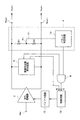
図1は、実施形態に係る低周波信号増幅装置の概略の回路構成を示す模式図である。BTL増幅器2は、入力端子NINから入力された信号を増幅し、反転出力端子NOUT−から反転出力信号VOUT−を出力し、一方、非反転出力端子NOUT+から非反転出力信号VOUT+を出力する。VOUT+及びVOUT−は同じ直流バイアスである基準バイアス電位Vb0に、交流信号成分が互いに逆相で重畳された信号となる。例えば、VOUT+の交流信号成分をVsigと表すと、VOUT+及びVOUT−は、次式で表される。なお、本実施形態では、Vb0は一例としてVCC/2に設定する。
FIG. 1 is a schematic diagram illustrating a schematic circuit configuration of a low-frequency signal amplifier according to an embodiment. BTL
VOUT+=Vb0+Vsig ………(1) V OUT + = V b0 + V sig (1)
VOUT−=Vb0−Vsig ………(2) V OUT− = V b0 −V sig (2)
増幅器保護回路は、中点判定回路4、範囲外状態検出回路6、AND回路8、制御回路10及びバイアス回路12を含んで構成される。
The amplifier protection circuit includes a midpoint determination circuit 4, an out-of-range state detection circuit 6, an AND circuit 8, a
中点判定回路4は、NOUT+及びNOUT−の間に直列接続された抵抗R1,R2と、R1及びR2の接続点P1の電位V1を入力されるバランス判定回路14とからなる。R1とR2との抵抗比は基本的に1:1に設定され、これにより、V1はVOUT+とVOUT−との中点電位となる。(1)(2)式で表されるVOUT+及びVOUT−が出力される正常動作時には、VOUT+及びVOUT−にて互いに逆相である信号成分VsigはP1点では相殺され、原理的に、V1は次式で示される一定の電位に保持される。
Midpoint determination circuit 4, and N OUT + and N resistors R1 connected in series between the OUT-, R2, consisting
V1=Vb0 ………(3) V 1 = V b0 (3)
一方、NOUT+又はNOUT−が誤接続状態となると、基本的にV1は(3)式で表される電位からずれる。例えば、NOUT+又はNOUT−が天絡状態となった場合、その直流バイアス電位はVCCとなり、P1点のバイアス電位は(Vb0+VCC)/2に上昇する。また、NOUT+又はNOUT−が地絡状態となった場合、その直流バイアス電位はGND(0V)となり、P1点のバイアス電位はVb0/2に低下する。 On the other hand, when N OUT + or N OUT− is in an erroneous connection state, V 1 basically deviates from the potential represented by the expression (3). For example, when N OUT + or N OUT− becomes a power fault state, the DC bias potential becomes V CC , and the bias potential at the point P 1 rises to (V b0 + V CC ) / 2. Further, when N OUT + or N OUT− is in a ground fault state, the DC bias potential becomes GND (0 V), and the bias potential at the point P 1 drops to V b0 / 2.
バランス判定回路14は、この正常状態と誤接続状態とでのV1の差異を判別し、正常状態では、論理値“0”を表す低電圧L(Low)を出力し、誤接続状態では、論理値“1”を表す高電圧H(High)を出力する。
The
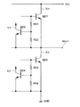
図2は、バランス判定回路14の構成の一例を示す概略の回路図である。入力端子INに入力されたV1は、pnpトランジスタQ1及びnpnトランジスタQ2それぞれのベースに印加される。Q1のエミッタ及びQ2のエミッタは互いに基準電圧源Vrefに接続される。VrefはVCCとGNDとの間の電圧に設定される。Q1のコレクタは、抵抗R3を介してGNDに接続される。R3は、Q1のコレクタに接続される側の一方端を、バランス判定回路14の出力端子OUTに接続され、他方端をGNDに接続される。
FIG. 2 is a schematic circuit diagram showing an example of the configuration of the
Q2のコレクタは、ダイオード接続とされたトランジスタQ3を介してVCCに接続される。トランジスタQ3はトランジスタQ4と共にカレントミラー回路を構成する。このカレントミラー回路の出力側経路のQ4は、上述のQ1と同じくR3の一方端に接続される。この構成により、R3に、Q1のコレクタ電流とQ2のコレクタ電流とを同じ向きに流すことができる。 The collector of Q2 is connected to V CC through transistor Q3 which is diode-connected. Transistor Q3 forms a current mirror circuit together with transistor Q4. Q4 of the output side path of this current mirror circuit is connected to one end of R3 as with Q1 described above. With this configuration, the collector current of Q1 and the collector current of Q2 can be supplied to R3 in the same direction.
このバランス判定回路14は、V1がVrefの近傍にあるときは、Q1及びQ2のいずれもオフ状態となり、R3に電流が流れないため、OUTからLレベルの電位としてGND電位を出力する。一方、V1がVrefより0.6V程度低くなるとQ1がオンし、Q1の電流がR3に流れ、OUTの電位はLレベルよりR3での電圧降下分だけ高いHレベルとなる。また、V1がVrefより0.6V程度高くなるとQ2がオンし、Q2の電流がカレントミラー回路で折り返されてR3に流れることにより、OUTの電位は、やはりLレベルより高いHレベルとなる。
When V 1 is in the vicinity of V ref , this
基準バイアス電位Vb0の入力時にバランス判定回路14がLレベルを出力するように、VrefはVb0の近傍に設定される。例えば、VrefはVb0に等しく設定することができる。VrefをVb0の近傍に設定することで、バランス判定回路14は、正常状態にて基準バイアス電位Vb0に維持されるV1と、誤接続状態にて基準バイアス電位Vb0から大きくずれるV1とを判別し、正常状態ではLレベルを、また誤接続状態ではHレベルをOUTから出力する。
V ref is set in the vicinity of V b0 so that the
次に、範囲外状態検出回路6は、NOUT+及びNOUT−の電位をそれぞれ監視し、それら電位のいずれかが所定の許容範囲(許容バイアス範囲)からはずれると、Hレベルを出力し、両電位が許容バイアス範囲内にあるときは、Lレベルを出力する。 Next, the out-of-range state detection circuit 6 monitors the potentials of N OUT + and N OUT− , and outputs an H level when either of these potentials deviates from a predetermined allowable range (allowable bias range). When the potential is within the allowable bias range, the L level is output.
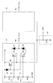
図3は、範囲外状態検出回路6の構成の一例を示す概略の回路図である。範囲外状態検出回路6は、入力端子IN+をNOUT+に接続されVOUT+を監視する非反転側の検出ブロック20と、入力端子IN−をNOUT−に接続されVOUT−を監視する反転側の検出ブロック22と、それら両検出ブロック20,22の出力信号をまとめる検出信号出力部24とを含んで構成される。
FIG. 3 is a schematic circuit diagram showing an example of the configuration of the out-of-range state detection circuit 6. Range state detection circuit 6, and the non-inverting side of the
図3には、非反転側の検出ブロック20について具体的な回路構成例を示しており、以下、この構成を説明する。なお、反転側の検出ブロック22は、基本的に非反転側の検出ブロック20と同一の回路構成とすることができ、ここでは図示及び説明を省略する。
FIG. 3 shows a specific circuit configuration example of the
検出ブロック20は、VCCとGNDとの間に直列に接続された抵抗R4,R5,R6を有する。R4とR5との接続点P2の電位V2は、許容バイアス範囲の上限に応じて設定され、R5とR6との接続点P3の電位V3は、許容バイアス範囲の下限に応じて設定される。
The
接続点P2にはpnpトランジスタQ5のベースが接続され、接続点P3にはnpnトランジスタQ6のベースが接続される。VOUT+を入力されるIN+は、ダイオードD1を介してQ5のエミッタに接続され、また、ダイオードD2を介してQ6のエミッタに接続される。D1は、VOUT+がP2の電位V2を上回る電位にて順方向バイアスとなり、D2は、VOUT+がP3の電位V3を下回る電位にて順方向バイアスとなる向きに設けられる。 The connection point P 2 is connected to the base of the pnp transistors Q5, the connection point P 3 the base of the npn transistor Q6 is connected. IN + to which V OUT + is input is connected to the emitter of Q5 through the diode D1, and is connected to the emitter of Q6 through the diode D2. D1 is, V OUT + is forward biased at a potential greater than the potential V 2 of P 2, D2 is, V OUT + is provided in the direction which becomes forward biased at a potential below the potential V 3 of the P 3.
Q5は、VOUT+が許容バイアス範囲の上限を上回るとオンし、そのコレクタ電流が出力端子から、検出信号出力部24に流れる。検出信号出力部24は、検出ブロック20から出力される電流を抵抗R7で正電圧に変換し出力する。
Q5 is turned on when V OUT + exceeds the upper limit of the allowable bias range, and the collector current flows from the output terminal to the detection
Q6は、VOUT+が許容バイアス範囲の下限を下回るとオンする。Q6のコレクタ電流は、ダイオードD3とトランジスタQ8とからなるカレントミラー回路によって折り返され、Q5のオン時のコレクタ電流と同じ向きの電流とされ、出力端子から検出信号出力部24へ出力される。検出信号出力部24は、この場合も、上述のQ5のオン時と同様に、Hレベルを出力する。
Q6 turns on when V OUT + falls below the lower limit of the allowable bias range. The collector current of Q6 is turned back by a current mirror circuit composed of a diode D3 and a transistor Q8, and the current is in the same direction as the collector current when Q5 is on, and is output from the output terminal to the detection
検出信号出力部24には、上述した非反転側の検出ブロック20と並列に反転側の検出ブロック22が接続される。この検出ブロック22は、VOUT−が許容バイアス範囲の上限を上回ったとき、及び下限を下回ったときに、検出ブロック20と同様に電流を出力し、これに応じて検出信号出力部24はHレベルを出力する。
An inversion
一方、VOUT+及びVOUT−のいずれもが、許容バイアス範囲内にある状態では、検出ブロック20,22のQ5,Q6はオフ状態にあり、基本的にR7に電流が流れず、R7の端子間電圧は0Vに保たれ、検出信号出力部24はLレベルを出力する。
On the other hand, when both V OUT + and V OUT− are within the allowable bias range, Q 5 and Q 6 of the detection blocks 20 and 22 are in an off state, and basically no current flows through
VOUT+及びVOUT−は、天絡時にはVCCに応じた電位となり、地絡時にはGNDに応じた電位となる。これに対応して、範囲外状態検出回路6は、天絡状態、地絡状態が継続する間、基本的に持続的にHレベルを出力する。一方、正常状態では、Vsigの振幅が許容バイアス範囲をはみ出す期間のみHレベルとなり、その他の期間はLレベルとなる。すなわち、範囲外状態検出回路6は、正常状態では基本的にHレベルを継続的に出力しない。本低周波信号増幅装置は、誤接続状態と正常状態とで異なる特徴を示す範囲外状態検出回路6の出力を、中点判定回路4の出力と共に、誤接続状態の検出に利用する。 V OUT + and V OUT- becomes a potential corresponding to V CC is in heaven fault occurs, the potential corresponding to GND to ground fault. In response to this, the out-of-range state detection circuit 6 basically outputs the H level continuously while the power supply state and the ground fault state continue. On the other hand, in the normal state, the amplitude of V sig becomes H level only during the period when it exceeds the allowable bias range, and becomes L level during the other periods. That is, the out-of-range state detection circuit 6 basically does not continuously output the H level in the normal state. This low-frequency signal amplifying apparatus uses the output of the out-of-range state detection circuit 6 showing different characteristics between the erroneous connection state and the normal state, together with the output of the midpoint determination circuit 4, for detection of the erroneous connection state.
AND回路8は、中点判定回路4の出力信号と範囲外状態検出回路6の出力信号とを入力され、それらの論理積に応じた信号を出力する。 The AND circuit 8 receives the output signal from the midpoint determination circuit 4 and the output signal from the out-of-range state detection circuit 6 and outputs a signal corresponding to the logical product of them.
制御回路10はAND回路8の出力信号に基づいて、NOUT+又はNOUT−における天絡、地絡の発生の有無を判断し、バイアス回路12のオン/オフを制御する。
Based on the output signal of the AND circuit 8, the
バイアス回路12は、BTL増幅器2にバイアス電源を供給する回路である。バイアス回路12から供給されるバイアス電源により、BTL増幅器2の出力トランジスタが駆動され、またVOUT+及びVOUT−の直流バイアス電位が基準バイアス電位Vb0に設定される。
The
制御回路10は、中点判定回路4及び範囲外状態検出回路6の双方がHレベルとなる状態をAND回路8が検出すると、その出力をセット入力部Sに受け、バイアス回路12をオフする。バイアス回路12がオフすることで、BTL増幅器2に誤接続に起因する過大な電流が流れることが防止され、BTL増幅器2の保護が図られる。また、制御回路10は、そのリセット入力部Rに、範囲外状態検出回路6がLレベルになったことを示す信号を受けると、バイアス回路12をオン状態にし正常動作に復帰させる。
When the AND circuit 8 detects a state in which both the midpoint determination circuit 4 and the out-of-range state detection circuit 6 are at the H level, the
上述の構成において、正常状態でのV1は原理的にはVOUT+及びVOUT−の中点電位となり、交流信号成分を相殺された直流信号である基準バイアス電位Vb0に維持される。そのため、原理的には、中点判定回路4の出力は、正常状態にてLレベルに保たれ、範囲外状態検出回路6は不必要であるかのようにも思われる。しかし、現実には、V1は種々の要因でVb0の近傍にて変動する可能性がある。中点判定回路4がLレベルを出力する入力信号電位の幅は比較的小さく、中点判定回路4は、正常状態でのV1の変動によってもHレベルを出力することがあり得る。すなわち、中点判定回路4だけでは、天絡、地絡といった誤接続状態を誤検出することが考えられる。 In the above configuration, V 1 in the normal state is in principle the midpoint potential of V OUT + and V OUT− , and is maintained at the reference bias potential V b0 which is a DC signal with the AC signal component canceled. Therefore, in principle, the output of the midpoint determination circuit 4 is maintained at the L level in a normal state, and it seems as if the out-of-range state detection circuit 6 is unnecessary. However, in reality, V 1 may fluctuate in the vicinity of V b0 due to various factors. Width of the input signal potential midpoint determination circuit 4 outputs an L level is relatively small, the midpoint determination circuit 4, there may be also outputs the H-level by variations in V 1 of the normal state. That is, it is conceivable that only the midpoint determination circuit 4 erroneously detects an erroneous connection state such as a power fault or a ground fault.
これに対し、本低周波信号増幅装置では、中点判定回路4とは異なる動作をする範囲外状態検出回路6を設け、両者の論理積に基づいて誤接続状態を検出することとして、誤検出により保護回路が誤動作することを抑制している。つまり、範囲外状態検出回路6は、正常状態では基本的に一時的にしかHレベルを出力しないので、正常状態にて中点判定回路4及び範囲外状態検出回路6の双方の出力がHレベルとなり誤検出を生じる可能性は、中点判定回路4のみの構成の誤検出の可能性より抑えられる。 On the other hand, in this low frequency signal amplifying device, an out-of-range state detection circuit 6 that operates differently from the midpoint determination circuit 4 is provided, and an erroneous detection is detected based on the logical product of both. This prevents the protection circuit from malfunctioning. That is, the out-of-range state detection circuit 6 basically outputs the H level only temporarily in the normal state, so that the outputs of both the midpoint determination circuit 4 and the out-of-range state detection circuit 6 are at the H level in the normal state. Therefore, the possibility of erroneous detection is suppressed from the possibility of erroneous detection of the configuration of only the midpoint determination circuit 4.
また、範囲外状態検出回路6のみを用い、そのHレベル出力が一定の猶予時間以上継続する場合を誤接続状態として、保護回路を動作させる構成も考えられるが、その構成では、判定を下すまでに一定時間が必要で、迅速な判定が困難である。その結果、保護回路の動作までの時間が長くなり、その間にBTL増幅器2に悪影響が発生する可能性が高くなる。特に、BTL増幅器2が増幅の対象とする信号Vsigが低周波であるほど猶予時間を長く設定する必要があり、保護回路によってBTL増幅器2が効果的に保護されなくなり得る。
In addition, a configuration is possible in which only the out-of-range state detection circuit 6 is used and the protection circuit is operated with the H level output continuing for a certain grace period or more as an erroneous connection state. It takes a certain amount of time to make a quick decision. As a result, the time until the protection circuit operates becomes longer, and the possibility that the
これに対し、本低周波信号増幅装置で用いる上述の保護回路は、誤接続状態を迅速、かつ上述のように高い信頼性で検出することで、BTL増幅器2を効果的に保護することが可能である。
On the other hand, the above-described protection circuit used in the present low-frequency signal amplifying device can effectively protect the
2 BTL増幅器、4 中点判定回路、6 範囲外状態検出回路、8 AND回路、10 制御回路、12 バイアス回路、14 バランス判定回路、20,22 検出ブロック、24 検出信号出力部。 2 BTL amplifier, 4 midpoint determination circuit, 6 out-of-range state detection circuit, 8 AND circuit, 10 control circuit, 12 bias circuit, 14 balance determination circuit, 20, 22 detection block, 24 detection signal output unit.
Claims (2)
前記反転出力端子の電位と前記非反転出力端子の電位とに基づいて、それらの中点である中点電位を求め、当該中点電位が前記基準バイアス電位に対し均衡状態にあるか不均衡状態にあるかを判定する中点判定回路と、
前記反転出力信号又は前記非反転出力信号が前記許容バイアス範囲外の電位となる範囲外状態を検出する範囲外状態検出回路と、
前記不均衡状態かつ前記範囲外状態であることに基づいて、前記BLT増幅器に対する保護動作を実行する保護実行回路と、
を有することを特徴とする増幅器保護回路。 A BTL amplifier that outputs an inverted output signal and a non-inverted output signal at a predetermined reference bias potential from each of the inverted output terminal and the non-inverted output terminal is outside the allowable bias range applied to the inverted output terminal or the non-inverted output terminal. A protection circuit that protects against the potential of
Based on the potential of the inverting output terminal and the potential of the non-inverting output terminal, a midpoint potential that is the midpoint between them is obtained, and whether the midpoint potential is in an equilibrium state with respect to the reference bias potential. A midpoint determination circuit for determining whether or not
An out-of-range state detection circuit that detects an out-of-range state in which the inverted output signal or the non-inverted output signal is at a potential outside the allowable bias range;
A protection execution circuit that performs a protection operation on the BLT amplifier based on the unbalanced state and the out-of-range state;
An amplifier protection circuit comprising:
前記BTL増幅器は、バイアス回路が供給する電源に基づいて、前記基準バイアス電位にて動作し、
前記保護実行回路は、前記保護動作として前記バイアス回路を停止させること、
を特徴とする増幅器保護回路。 The amplifier protection circuit of claim 1.
The BTL amplifier operates at the reference bias potential based on a power source supplied by a bias circuit,
The protection execution circuit stops the bias circuit as the protection operation;
An amplifier protection circuit.
Priority Applications (1)
| Application Number | Priority Date | Filing Date | Title |
|---|---|---|---|
| JP2006349345A JP2008160661A (en) | 2006-12-26 | 2006-12-26 | Amplifier protection circuit |
Applications Claiming Priority (1)
| Application Number | Priority Date | Filing Date | Title |
|---|---|---|---|
| JP2006349345A JP2008160661A (en) | 2006-12-26 | 2006-12-26 | Amplifier protection circuit |
Publications (1)
| Publication Number | Publication Date |
|---|---|
| JP2008160661A true JP2008160661A (en) | 2008-07-10 |
Family
ID=39661040
Family Applications (1)
| Application Number | Title | Priority Date | Filing Date |
|---|---|---|---|
| JP2006349345A Pending JP2008160661A (en) | 2006-12-26 | 2006-12-26 | Amplifier protection circuit |
Country Status (1)
| Country | Link |
|---|---|
| JP (1) | JP2008160661A (en) |
Cited By (3)
| Publication number | Priority date | Publication date | Assignee | Title |
|---|---|---|---|---|
| JP2016519552A (en) * | 2013-05-24 | 2016-06-30 | 日本テキサス・インスツルメンツ株式会社 | Power amplifier control circuit |
| JP2017083992A (en) * | 2015-10-26 | 2017-05-18 | 株式会社デンソー | Constant voltage power circuit |
| JP7579018B1 (en) | 2023-07-11 | 2024-11-07 | 株式会社ビートソニック | Impedance adjustment device for audio systems |
-
2006
- 2006-12-26 JP JP2006349345A patent/JP2008160661A/en active Pending
Cited By (4)
| Publication number | Priority date | Publication date | Assignee | Title |
|---|---|---|---|---|
| JP2016519552A (en) * | 2013-05-24 | 2016-06-30 | 日本テキサス・インスツルメンツ株式会社 | Power amplifier control circuit |
| JP2017083992A (en) * | 2015-10-26 | 2017-05-18 | 株式会社デンソー | Constant voltage power circuit |
| JP7579018B1 (en) | 2023-07-11 | 2024-11-07 | 株式会社ビートソニック | Impedance adjustment device for audio systems |
| JP2025011701A (en) * | 2023-07-11 | 2025-01-24 | 株式会社ビートソニック | Impedance adjustment device for audio systems |
Similar Documents
| Publication | Publication Date | Title |
|---|---|---|
| US5905617A (en) | Differential amplifier having a protection circuit | |
| JP2003254850A (en) | Sensor output processing circuit with self-diagnosis function | |
| US7821245B2 (en) | Voltage transformation circuit | |
| JP2876854B2 (en) | Potential detection circuit | |
| JP2008160661A (en) | Amplifier protection circuit | |
| JP2006064596A (en) | Current detector | |
| JP5819212B2 (en) | Load connection status detection circuit | |
| US8120414B2 (en) | Low-noise current source | |
| JP2021141443A (en) | Semiconductor integrated circuit device and current detection circuit | |
| JP2021022917A (en) | Semiconductor device | |
| JP3451954B2 (en) | Voltage comparison circuit | |
| US10063217B2 (en) | Current-to-voltage conversion circuit and self-oscillation circuit | |
| JP4360267B2 (en) | Amplifier circuit | |
| JP2011174787A (en) | Current controller and current detector | |
| JP6625458B2 (en) | Output circuit and current sensor having the same | |
| JP3648702B2 (en) | Power amplifier IC and audio system | |
| JP2001108712A (en) | Current detector | |
| JP3860089B2 (en) | DC stabilized power supply circuit | |
| JP4258837B2 (en) | 2-wire transmission circuit | |
| JP4941718B2 (en) | Voltage shift circuit | |
| US20050151569A1 (en) | Output circuit and operational amplifier | |
| JP2006349466A (en) | Temperature detection device | |
| JP3664038B2 (en) | Reset circuit | |
| JP2023121617A (en) | semiconductor equipment | |
| JPH0119284B2 (en) |