JP2008158366A - Plasma display device - Google Patents
Plasma display device Download PDFInfo
- Publication number
- JP2008158366A JP2008158366A JP2006348744A JP2006348744A JP2008158366A JP 2008158366 A JP2008158366 A JP 2008158366A JP 2006348744 A JP2006348744 A JP 2006348744A JP 2006348744 A JP2006348744 A JP 2006348744A JP 2008158366 A JP2008158366 A JP 2008158366A
- Authority
- JP
- Japan
- Prior art keywords
- pulse
- voltage
- sustain
- superimposed
- sustain discharge
- Prior art date
- Legal status (The legal status is an assumption and is not a legal conclusion. Google has not performed a legal analysis and makes no representation as to the accuracy of the status listed.)
- Pending
Links
Images
Classifications
-
- G—PHYSICS
- G09—EDUCATION; CRYPTOGRAPHY; DISPLAY; ADVERTISING; SEALS
- G09G—ARRANGEMENTS OR CIRCUITS FOR CONTROL OF INDICATING DEVICES USING STATIC MEANS TO PRESENT VARIABLE INFORMATION
- G09G3/00—Control arrangements or circuits, of interest only in connection with visual indicators other than cathode-ray tubes
- G09G3/20—Control arrangements or circuits, of interest only in connection with visual indicators other than cathode-ray tubes for presentation of an assembly of a number of characters, e.g. a page, by composing the assembly by combination of individual elements arranged in a matrix no fixed position being assigned to or needed to be assigned to the individual characters or partial characters
- G09G3/22—Control arrangements or circuits, of interest only in connection with visual indicators other than cathode-ray tubes for presentation of an assembly of a number of characters, e.g. a page, by composing the assembly by combination of individual elements arranged in a matrix no fixed position being assigned to or needed to be assigned to the individual characters or partial characters using controlled light sources
- G09G3/28—Control arrangements or circuits, of interest only in connection with visual indicators other than cathode-ray tubes for presentation of an assembly of a number of characters, e.g. a page, by composing the assembly by combination of individual elements arranged in a matrix no fixed position being assigned to or needed to be assigned to the individual characters or partial characters using controlled light sources using luminous gas-discharge panels, e.g. plasma panels
- G09G3/288—Control arrangements or circuits, of interest only in connection with visual indicators other than cathode-ray tubes for presentation of an assembly of a number of characters, e.g. a page, by composing the assembly by combination of individual elements arranged in a matrix no fixed position being assigned to or needed to be assigned to the individual characters or partial characters using controlled light sources using luminous gas-discharge panels, e.g. plasma panels using AC panels
- G09G3/291—Control arrangements or circuits, of interest only in connection with visual indicators other than cathode-ray tubes for presentation of an assembly of a number of characters, e.g. a page, by composing the assembly by combination of individual elements arranged in a matrix no fixed position being assigned to or needed to be assigned to the individual characters or partial characters using controlled light sources using luminous gas-discharge panels, e.g. plasma panels using AC panels controlling the gas discharge to control a cell condition, e.g. by means of specific pulse shapes
- G09G3/294—Control arrangements or circuits, of interest only in connection with visual indicators other than cathode-ray tubes for presentation of an assembly of a number of characters, e.g. a page, by composing the assembly by combination of individual elements arranged in a matrix no fixed position being assigned to or needed to be assigned to the individual characters or partial characters using controlled light sources using luminous gas-discharge panels, e.g. plasma panels using AC panels controlling the gas discharge to control a cell condition, e.g. by means of specific pulse shapes for lighting or sustain discharge
- G09G3/2942—Control arrangements or circuits, of interest only in connection with visual indicators other than cathode-ray tubes for presentation of an assembly of a number of characters, e.g. a page, by composing the assembly by combination of individual elements arranged in a matrix no fixed position being assigned to or needed to be assigned to the individual characters or partial characters using controlled light sources using luminous gas-discharge panels, e.g. plasma panels using AC panels controlling the gas discharge to control a cell condition, e.g. by means of specific pulse shapes for lighting or sustain discharge with special waveforms to increase luminous efficiency
-
- G—PHYSICS
- G09—EDUCATION; CRYPTOGRAPHY; DISPLAY; ADVERTISING; SEALS
- G09G—ARRANGEMENTS OR CIRCUITS FOR CONTROL OF INDICATING DEVICES USING STATIC MEANS TO PRESENT VARIABLE INFORMATION
- G09G3/00—Control arrangements or circuits, of interest only in connection with visual indicators other than cathode-ray tubes
- G09G3/20—Control arrangements or circuits, of interest only in connection with visual indicators other than cathode-ray tubes for presentation of an assembly of a number of characters, e.g. a page, by composing the assembly by combination of individual elements arranged in a matrix no fixed position being assigned to or needed to be assigned to the individual characters or partial characters
- G09G3/22—Control arrangements or circuits, of interest only in connection with visual indicators other than cathode-ray tubes for presentation of an assembly of a number of characters, e.g. a page, by composing the assembly by combination of individual elements arranged in a matrix no fixed position being assigned to or needed to be assigned to the individual characters or partial characters using controlled light sources
- G09G3/28—Control arrangements or circuits, of interest only in connection with visual indicators other than cathode-ray tubes for presentation of an assembly of a number of characters, e.g. a page, by composing the assembly by combination of individual elements arranged in a matrix no fixed position being assigned to or needed to be assigned to the individual characters or partial characters using controlled light sources using luminous gas-discharge panels, e.g. plasma panels
- G09G3/288—Control arrangements or circuits, of interest only in connection with visual indicators other than cathode-ray tubes for presentation of an assembly of a number of characters, e.g. a page, by composing the assembly by combination of individual elements arranged in a matrix no fixed position being assigned to or needed to be assigned to the individual characters or partial characters using controlled light sources using luminous gas-discharge panels, e.g. plasma panels using AC panels
- G09G3/296—Driving circuits for producing the waveforms applied to the driving electrodes
Landscapes
- Engineering & Computer Science (AREA)
- Physics & Mathematics (AREA)
- Power Engineering (AREA)
- Plasma & Fusion (AREA)
- Computer Hardware Design (AREA)
- General Physics & Mathematics (AREA)
- Theoretical Computer Science (AREA)
- Control Of Indicators Other Than Cathode Ray Tubes (AREA)
- Control Of Gas Discharge Display Tubes (AREA)
Abstract
【課題】
高電圧の細幅パルスとこれに伴う低電圧の広幅パルスとからなる高発光効率が得られる維持放電駆動波形を用いて、大型のPDPを良好に駆動できるプラズマディスプレイ装置を提供する。
【解決手段】
サステイン期間に維持放電電極間に印加されるサステインパルスを、ベースパルス(P2)と、このベースパルス(P2)の前縁部に重畳される重畳パルス(P1)で構成する。重畳パルス(P1)は、かつ維持放電を開始させるための電圧(Vp)と、壁電荷を形成して維持放電を停止させるための電圧(Vsu)との差電圧(Vdif)を持ち、かつ維持放電の開始から自己停止までの期間よりも短いパルス幅(T1)を持つ。またベースパルス(P2)は、上記T1とこのT1よりも大きいT2の和に等しいパルス幅(Ts)を持ち、かつ上記電圧(Vsu)を有する。
【選択図】図1【Task】
Provided is a plasma display device capable of satisfactorily driving a large PDP by using a sustain discharge driving waveform that provides a high luminous efficiency comprising a high-voltage narrow pulse and a low-voltage wide pulse associated therewith.
[Solution]
A sustain pulse applied between the sustain discharge electrodes in the sustain period is composed of a base pulse (P2) and a superposed pulse (P1) superposed on the leading edge of the base pulse (P2). The superimposed pulse (P1) has a voltage difference (Vdif) between the voltage (Vp) for starting the sustain discharge and the voltage (Vsu) for forming the wall charge and stopping the sustain discharge, and is maintained. It has a shorter pulse width (T1) than the period from the start of discharge to self-stop. The base pulse (P2) has a pulse width (Ts) equal to the sum of T1 and T2 larger than T1, and has the voltage (Vsu).
[Selection] Figure 1
Description
本発明は、AC型(交流型)プラズマディスプレイパネルを用いた表示装置であるプラズマディスプレイ装置に係わり、プラズマディスプレイパネルの発光効率を向上するために、維持放電期間に、高電圧の細幅パルスとこれに続く低電圧の広幅パルスとで構成されたサステインパルスで、プラズマディスプレイパネルを駆動する駆動回路に関係する。 The present invention relates to a plasma display device, which is a display device using an AC type (AC type) plasma display panel. In order to improve the luminous efficiency of the plasma display panel, a high voltage narrow pulse and This is related to a driving circuit for driving a plasma display panel with a sustain pulse composed of a low-voltage wide pulse following this.
プラズマディスプレイパネル(Plasma Display Panel:以下、「PDP」と略称する)、特に交流型(AC型)PDPにおいて、維持放電期間(サステイン期間)における放電効率を向上させるために、サステイン期間において走査電極(Y電極)と共通電極(X電極またはサステイン電極)間に印加される放電維持パルス(サステインパルス)の波形について改良を為した技術が、例えば特許文献1に開示されている。
In order to improve the discharge efficiency in the sustain discharge period (sustain period) in a plasma display panel (hereinafter abbreviated as “PDP”), particularly an AC type (AC type) PDP, a scan electrode ( For example,
特許文献1に開示された維持放電パルスは、第1電圧パルスと第2電圧パルスで構成されている。第1電圧パルスは、放電を開始させるに十分な電圧レベルを有し、かつこの放電で形成された壁電荷による逆電界の発生によって、放電が自己停止に至る時間より短いパルス幅(例えば0.6μS程度)を有している(以下、「細幅パルス」という)。第2電圧パルスは、上記細幅パルスで発生した放電を継続できる電圧よりも低い電圧レベルを有し、かつ細幅パルスによる放電によって生成された空間電荷の一部が壁電荷として付着するようなパルス幅(例えば2〜3μS程度)を有している(以下、「広幅パルス」という)。
The sustain discharge pulse disclosed in
このようなサステインパルスを形成するための回路の一例が、例えば特許文献2に開示されている。特許文献2は、上記細幅パルスを発生させるために、その図7のように、直流電源SVpから、スイッチp1,コイルL,PDPが有する容量(以下、「パネル容量」と称する)Cpanelを直列接続の構成にすること、及びスイッチp1のオン時に、電源SVpからコイルLを通じてパネル容量Cpanelを充電する共振動作で、サステイン電極に電源電圧SVpの2倍の電圧を発生させることを開示する。
An example of a circuit for forming such a sustain pulse is disclosed in
特許文献1に記載の技術を例えば42インチのPDPに適用する場合、細幅パルス(例えば約160V,約0.5μS)を、パネル容量(42インチのサステイン電極を垂直方向に2分割で約0.05μF)に印加して、その間に放電電流(数十Aピーク)を流すためには、立ち上がり時間0.1〜0.2μSの間に、パネル容量を約160Vまで充電して、その後放電させなければならない。そのためには、オン/ オフスピードが早い半導体スイッチが必要であり、実現が容易ではない。一般に、半導体は、オン/オフスピードが早くなる程耐電圧が低くなり、耐電圧150Vを越えるような高速大電流半導体素子は高価でありIC化することも難しい。
When the technique described in
一方、特許文献2では、コイルLとパネル容量CpanelとでLC直列共振回路を構成し、共振現象を利用して細幅パルスを形成しているが、この直列共振回路には、サステイン電極に存在する寄生抵抗Rが含まれる。実際のサステイン電極に寄生している寄生抵抗Rは、PDPが大型になればなるほど大きくなり、例えば42インチパネルで数〜数十Ωあると考えられる。寄生抵抗Rが大きいと、LC直列共振回路のQ(Quality factor:ωL/R)が小さくなり、例えば電圧値約160Vを有する細幅パルスを生成することが困難となる。従って、LC直列共振回路で細幅パルスを生成する技術は、例えば42インチを越えるような大型のPDPになる程、適用が難しくなる。
On the other hand, in
本発明は、上記課題に鑑みてなされたもので、その目的は、プラズマディスプレイ装置において、細幅パルスを用いて大型のPDPを良好に駆動できる技術を提供することにある。 The present invention has been made in view of the above problems, and an object of the present invention is to provide a technique capable of satisfactorily driving a large PDP using a narrow pulse in a plasma display device.
上記目的を達成するための本発明に係るプラズマディスプレイ装置は、細幅パルス(パルス幅t1、電圧Vp)と広幅パルスの(パルス幅t2、電圧Vsu)とで構成されるサステインパルスを発生するために、電圧Vsuを持ち、かつパルス幅(t1+t2)のベースパルスを発生するベースパルス発生部と、ベースパルスの前縁部に重畳される、電圧(Vp−Vsu)持ち、かつパルス幅t1の重畳パルスを発生する重畳パルス発生部を設けたことを特徴とするものである。 In order to achieve the above object, a plasma display apparatus according to the present invention generates a sustain pulse composed of a narrow pulse (pulse width t1, voltage Vp) and a wide pulse (pulse width t2, voltage Vsu). In addition, a base pulse generator having a voltage Vsu and generating a base pulse having a pulse width (t1 + t2), and a voltage (Vp−Vsu) having a voltage (Vp−Vsu) superimposed on the leading edge of the base pulse, are superimposed. A superimposed pulse generation unit for generating a pulse is provided.
また上記重畳パルス生成部の基準電位を前記ベースパルス生成部の基準電位に対してフローティングさせてもよい。 Further, the reference potential of the superimposed pulse generation unit may be floated with respect to the reference potential of the base pulse generation unit.
これにより、重畳パルスの波高値電圧(Vp−Vsu)を小さくすることができ、重畳パルスを高速動作可能な半導体スイッチ(例えば高速スイッチング用のMOSトランジスタ)を用いて生成することが可能となる。従って、大型のPDPであっても、LC直列共振回路を用いることなく、好適なサステインパルスを形成することができる。また波形発生に能動素子を用いることで制御可能となる為、動作の最適化のために波形を調整することも可能となる。 As a result, the peak voltage (Vp−Vsu) of the superimposed pulse can be reduced, and the superimposed pulse can be generated using a semiconductor switch (for example, a MOS transistor for high-speed switching) that can operate at high speed. Therefore, even with a large PDP, a suitable sustain pulse can be formed without using an LC series resonance circuit. Further, since the active element can be used for generating the waveform, the waveform can be adjusted to optimize the operation.
以上述べたように、本発明によれば、細幅パルスを用いて大型のPDPを良好に駆動できる。 As described above, according to the present invention, a large PDP can be satisfactorily driven using narrow pulses.
以下、本発明の実施形態について、図を用いて詳細に説明する。尚、全図において、共通な機能を有する部分には同一符号を付して示し、一度説明したものについては、煩雑さを避けるため、繰り返した説明を省略する。 Hereinafter, embodiments of the present invention will be described in detail with reference to the drawings. In all the drawings, parts having common functions are denoted by the same reference numerals, and once described, repeated description is omitted to avoid complexity.
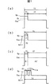
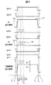
まず、本実施形態の概要について、図1を用いて説明する。図1は、本発明によるプラズマディスプレイ装置のサステイン期間におけるPDPの電圧駆動波形を説明する図である。 First, an outline of the present embodiment will be described with reference to FIG. FIG. 1 is a diagram illustrating a voltage driving waveform of a PDP during a sustain period of the plasma display apparatus according to the present invention.
図1(a)に示す駆動波形は、サステインパルスとして、特許文献1で開示された細幅パルスと広幅パルスとを組み合せて構成した場合における電圧駆動波形である。かかるサステインパルスは、図1(c)に示すように、細幅パルスP1’と広幅パルスP2’で構成される。細幅パルスP1’は、維持放電(サステイン放電ともいう)を開始させるに十分な高電圧Vpを有する。更に、維持放電の開始から、維持放電で形成された壁電荷による逆電界の発生によって維持放電が自己停止までの期間より短いパルス幅t1を有している。また広幅パルスP2’は、細幅パルスP1’で発生した維持放電を継続できる電圧よりも低く、かつ、維持放電によって生成された空間電荷の一部が壁電荷として付着するような低電圧Vsuを有する。更に広幅パルスP2’は、パルス幅t1よりも長いパルス幅t2を有している。なお、電圧Vsは、維持放電を開始させるためにPDPに印加される従来のサステインパルス(パルス幅ts:通常2〜3μS程度)の電圧レベルで、一般に、42インチのPDPでは、約160〜220V程度に設定される。
The drive waveform shown in FIG. 1A is a voltage drive waveform in the case where a narrow pulse and a wide pulse disclosed in
本実施形態では、図1(b)に示すように、前記電圧駆動波形を、低電圧Vsuを有するパルス幅(ts=t1+t2)の広幅パルス(以下、「ベースパルス」と称する)P2と、このベースパルスP2の前縁部に重畳され、電圧(Vp−Vsu)を持つとともにパルス幅t1の細幅パルス(以下、「重畳パルス」と称する)P1とで構成する。なお、具体的回路の詳細については後述するが、ベースパルスP2に重畳パルスP1を重畳するためには、重畳パルスP1を生成する重畳パルス生成部の基準電位(仮想GND)は、ベースパルスP2を生成するベースパルス生成部の基準電位(GND)に対して、フローティングさせる必要がある。 In this embodiment, as shown in FIG. 1B, the voltage drive waveform is divided into a wide pulse (hereinafter referred to as “base pulse”) P2 having a pulse width (ts = t1 + t2) having a low voltage Vsu, It is superimposed on the leading edge of the base pulse P2, and has a voltage (Vp−Vsu) and a narrow pulse (hereinafter referred to as “superimposed pulse”) P1 having a pulse width t1. Although details of a specific circuit will be described later, in order to superimpose the superimposed pulse P1 on the base pulse P2, the reference potential (virtual GND) of the superimposed pulse generation unit that generates the superimposed pulse P1 is the base pulse P2. It is necessary to float with respect to the reference potential (GND) of the base pulse generator to be generated.
広幅パルスであるベースパルスP2は、従来技術によるサステインパルスに略等しく、従来のサステイン回路で生成することができる。また、細幅パルスである重畳パルスP1は、その振幅電圧が電圧Vpと電圧Vsuとの差電圧Vdifでよい。このため、重畳パルスP1の電圧レベルを十分小さくすることが可能である。従って、スイッチング速度の早い半導体素子を集積化したIC技術を適用することができる。 The base pulse P2, which is a wide pulse, is substantially equal to the sustain pulse according to the prior art and can be generated by a conventional sustain circuit. Further, the superimposed pulse P1 which is a narrow pulse may have an amplitude voltage of a difference voltage Vdif between the voltage Vp and the voltage Vsu. For this reason, the voltage level of the superimposed pulse P1 can be made sufficiently small. Therefore, it is possible to apply IC technology in which semiconductor elements having a high switching speed are integrated.
上記したように、本実施例によれば、重畳パルスP1の波高値電圧(Vdif=Vp−Vsu)を小さくすることができ、重畳パルスを半導体スイッチ(例えばMOSトランジスタ)を用いて生成することでき、IC回路で構成することが可能となる。 As described above, according to this embodiment, the peak value voltage (Vdif = Vp−Vsu) of the superimposed pulse P1 can be reduced, and the superimposed pulse can be generated using a semiconductor switch (for example, a MOS transistor). It can be configured with an IC circuit.
なお、以下に述べる実施例では、図1(d)に示すように、重畳パルスP1として、複数の細幅パルス列を用いる。ここでは、例えば一例としてパルス幅t1a=100nS,IC化も可能となる振幅60〜70Vを有する細幅パルスを2個重畳する。しかし、本発明は、これに限定されるものではないことはいうまでもない。 In the embodiment described below, as shown in FIG. 1D, a plurality of narrow pulse trains are used as the superposed pulse P1. Here, as an example, two narrow pulses having a pulse width t1a = 100 nS and an amplitude of 60 to 70 V that can be made into an IC are superimposed. However, it goes without saying that the present invention is not limited to this.
発光効率は、特許文献1に記載の如く、パルス幅が狭くなる程向上する。しかし、パルス幅が狭いので、輝度が低下する恐れがある。そこで、本実施形態では、細幅パルスを複数個(ここでは2個)重畳して、放電を複数回(ここでは2回)引き起こし、輝度を従来とほぼ同等となるようにする。すなわち、複数個の細幅パルスを重畳することによって、発光効率の向上を図りながら、輝度を従来とほぼ同等とすることができる。
As described in
また、本実施例では、先頭の重畳パルスをベースパルスの先端(立ち上がりポイント)から所定時間t0をおいて重畳させるようにすることもでき、放電形態をシステムの要望に合せ自由に設定できる。 In the present embodiment, the leading superimposed pulse can be superimposed at a predetermined time t0 from the leading end (rising point) of the base pulse, and the discharge mode can be freely set according to the demand of the system.
次に、本発明による一実施例であるAC型PDPを用いたプラズマディスプレイ装置(以下、「PDP装置」と省略する)について説明する。なお、本実施例は、PDPの維持放電時における対をなすY電極とX電極からなるサステイン電極の駆動方法に係わるものである。従って、以下では、PDPを駆動するPDP周辺駆動部について説明するが、リセット期間やアドレス期間における駆動については概要を述べるに留め、維持放電の駆動に関して詳細に説明する。 Next, a plasma display device (hereinafter abbreviated as “PDP device”) using an AC type PDP according to an embodiment of the present invention will be described. This embodiment relates to a driving method of a sustain electrode composed of a pair of Y electrode and X electrode during sustain discharge of the PDP. Therefore, in the following description, the PDP peripheral driving unit that drives the PDP will be described. However, only the outline of the driving in the reset period and the address period will be described, and the driving of the sustain discharge will be described in detail.
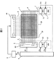
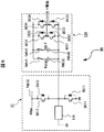
図2は、本発明による実施例1に係わるPDP装置におけるPDP駆動部の模式ブロック構成図である。 FIG. 2 is a schematic block configuration diagram of a PDP drive unit in the PDP apparatus according to the first embodiment of the present invention.
図2に示すように、PDP装置のPDP周辺駆動部は、PDP1と、PDP1をY電極3側から駆動する一方の維持放電駆動回路であるY駆動部6と、PDP1をX電極4側から駆動する他方の維持放電駆動回路であるX駆動部7と、タイミング制御部8と、画像処理部9と、アドレス駆動部10とを含んでなる。
As shown in FIG. 2, the PDP peripheral drive unit of the PDP device drives
PDP1は、互いに対向して配置された前面板2Fと背面板2Rとからなる。前面板2Fは、対を成すサステイン電極(維持電極)を構成するY電極3とX電極4を複数備えている。プラズマディスプレイ装置としては、前面板2Fを通して発光した光を見ることになる。Y電極3およびX電極4は、例えばガラス基板である前面板2Fの内面側に銀や銅などの金属電極とITOなどの透明電極がストライプ状に積層されて形成されたもので、それらの電極を覆うように誘電体(図示せず、ガラスを成分としている)が配置されている。
The
背面板2R上には、Y電極3とX電極4に直交するようにアドレス電極(以下、「A電極」と称する)5が形成されている。
Address electrodes (hereinafter referred to as “A electrodes”) 5 are formed on the
そして、対をなすサステイン電極(Y電極3とX電極4)と各A電極5との交点部分にそれぞれ画素となる図示しない表示セルが形成されている。
A display cell (not shown) serving as a pixel is formed at the intersection between the pair of sustain electrodes (
タイミング制御部8は、図示しない同期信号抽出回路からの同期信号に基づいて、種々のタイミング信号を生成する。種々のタイミング信号としては、例えば、アドレス期間のY電極走査(スキャン)に合せてA電極を制御するアドレス電極制御信号(以下、「A電極制御信号」と称する)85や、アドレス期間におけるスキャンを指示するスキャン制御信号83,維持放電駆動を行わせるサステイン制御信号などを生成する。サステイン制御信号には、ベースパルスP2の生成を制御するベースパルス制御信号81y,71xや重畳パルスP1の生成を制御する重畳パルス制御信号82y,72xなどが含まれる。
The timing control unit 8 generates various timing signals based on a synchronization signal from a synchronization signal extraction circuit (not shown). As various timing signals, for example, an address electrode control signal (hereinafter referred to as “A electrode control signal”) 85 for controlling the A electrode in accordance with the Y electrode scan (scan) in the address period, or a scan in the address period is used. A
一方の維持放電駆動回路であるY駆動部6は、Y電極に印加するベースパルスP2を生成するベースパルス生成部であるYサステイン回路61と、重畳パルスP1を生成する重畳パルス生成部であるY重畳パルス生成回路62と、スキャン回路63とを含んでなる。
The Y driving unit 6 that is one sustain discharge driving circuit is a Y sustain
スキャン回路63は、タイミング制御部8からのスキャン制御信号83に基づき、アドレス期間にY電極3のスキャン(走査)を行う。
The
Yサステイン回路61は、タイミング制御部7からのベースパルス制御信号81yを受けて、サステイン期間にY電極3を維持放電駆動するベースパルスP2を生成する。
The Y sustain
また、Y重畳パルス生成回路62は、タイミング制御部7からの重畳パルス制御信号82yを受けて、重畳パルスP1を生成し、図1(d)に示すように、ベースパルスP2の前縁部に生成した重畳パルスP1を重畳する。Y重畳パルス生成回路62の基準電位(仮想GND)は、重畳パルスP1をベースパルスP2に重畳するため、Yサステイン回路61の基準電位(基準GND)に対してフローティングされている(詳細は後述する)。
Further, the Y superimposed
他方の維持放電駆動回路であるX駆動部7は、X電極に印加するベースパルスP2を生成するベースパルス生成部であるXサステイン回路71と、重畳パルスP1を生成する重畳パルス生成部であるX重畳パルス生成回路72とを含んでなる。
The
Xサステイン回路71は、タイミング制御部7からのベースパルス制御信号81xを受けて、サステイン期間にX電極4を維持放電駆動するベースパルスP2を生成する。
The X sustain
また、X重畳パルス生成回路72は、タイミング制御部7からの重畳パルス制御信号82xを受けて、重畳パルスP2を生成し、図1(d)に示すように、ベースパルスP2の前縁部に生成した重畳パルスP1を重畳する。X重畳パルス生成回路72の基準電位(仮想GND)もまた、重畳パルスP1をベースパルスP2に重畳するため、Xサステイン回路71の基準電位(基準GND)に対してフローティングされている(詳細は後述する)。
In addition, the X superimposed
画像処理回路9は、入力された画像データ(図示せず)の1フィールドデータを複数のサブフィールドデータに変換する。そして、変換したサブフィールドデータをタイミング制御部8からのA電極制御信号85に基づいて、アドレス駆動部10に供給する。
The image processing circuit 9 converts one field data of input image data (not shown) into a plurality of subfield data. Then, the converted subfield data is supplied to the
アドレス駆動部10は、画像処理部9からの信号をY駆動部6のスキャン回路63によるスキャン(行走査)に同期して、サステイン期間に点灯させるべき表示セルに対応したA電極5にアドレスパルス(図示せず)を印加する。
The
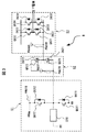
次に、図3,図4と図5を用いて、図1(d)に示した発光効率を高める維持放電駆動波形を生成するための駆動回路であるY駆動部6とX駆動部7の一実施例について説明する。
Next, with reference to FIGS. 3, 4, and 5, the Y drive unit 6 and the
図3は、本実施例によるY駆動部の要部を模式的に示した回路構成図、図4は、本実施例によるX駆動部の要部を模式的に示した回路構成図、図5は、本実施例における駆動回路の動作を説明するための各部のタイミング波形および出力波形である。 3 is a circuit configuration diagram schematically showing the main part of the Y drive unit according to the present embodiment, FIG. 4 is a circuit configuration diagram schematically showing the main part of the X drive unit according to the present embodiment, and FIG. These are the timing waveform and output waveform of each part for demonstrating operation | movement of the drive circuit in a present Example.
なお、図3,図4では、分かり易くするために、各回路の出力段のみ図示している。また、図3のスキャン回路は、各Y電極を駆動するために、Y電極数と同数の出力段を有するが、ここでは、便宜上2つの出力段のみを示し、その動作については、一つの出力段(ここでは、トランジスタQ631,Q632からなる出力段)を用いて説明する。また、サステイン期間におけるY駆動部6とX駆動部7の動作は、同じであり、以下では、PDP1をY電極側から駆動する場合における駆動回路の動作について説明する。
3 and 4, only the output stage of each circuit is shown for easy understanding. The scan circuit of FIG. 3 has the same number of output stages as the number of Y electrodes in order to drive each Y electrode, but here, only two output stages are shown for the sake of convenience. A description will be given using a stage (here, an output stage including transistors Q631 and Q632). The operations of the Y drive unit 6 and the
図3に示すように、ベースパルスを生成するYサステイン回路61は、電源PW618(電源電圧Vsu)と、電力回収回路616と、スイッチ用のトランジスタQ611,Q612とを含んでなる。また、重畳パルスを生成するY重畳パルス生成回路62は、フローティングした電源PW628(Y重畳パルス生成回路62の仮想GNDに対する電源電圧Vdif)と、スイッチ用のトランジスタQ621,622とを含んでなる。また、アドレス期間に走査(スキャン)を行うスキャン回路63は、フローティングした電源PW638(スキャン回路63の仮想GNDに対する電源電圧Vscan)と、スイッチ用のトランジスタQ631,Q632、Q633,Q634,…とを含んでなる。そして、各スイッチ用のトランジスタには、同一符番のダイオードが形成されている。
As shown in FIG. 3, the Y sustain
同様に、図4に示すように、ベースパルスを生成するXサステイン回路71は、電源PW718(電源電圧Vsu)と、電力回収回路716と、スイッチ用のトランジスタQ711,Q712とを含んでなる。また、重畳パルスを生成するX重畳パルス生成回路72は、フローティングした電源PW728(X重畳パルス生成回路72の仮想GNDに対する電源電圧Vdif)と、スイッチ用のトランジスタQ721,722とを含んでなる。そして、各スイッチ用のトランジスタには、同一符番のダイオードが形成されている。
Similarly, as shown in FIG. 4, the X sustain
なお、フローティングした電源は、例えば、絶縁トランス(図示せず)の2次巻線に得られる高周波パルスを整流することにより、容易に実現することができる。 The floating power supply can be easily realized by rectifying a high-frequency pulse obtained in a secondary winding of an insulating transformer (not shown), for example.
電力回収回路616/716は、周知の電力回収回路で構成され、ベースパルスP2の立ち上がり時に、以前回収しておいた電力でPDP1のパネル容量を充電するとともに、ベースパルスP2の立ち下がり時に、PDP1のパネル容量に充電されている電力を回収するものである。
The
スキャン回路63は、サステイン期間では、単なるスルー回路であり、PDP1に電流が流れる場合には、ダイオードD631,D633,…を通って電流が流れ、PDP1から電流が流れ込む場合には、下側のトランジスタQ631,Q633,…がオンして、Y重畳パルス生成回路62,Yサステイン回路61に流れ込む(詳細は後述する)。
The
また、重畳パルス生成回路62,72は、重畳パルスを生成しない期間においては、スキャン回路63と同様に、サステイン回路61,71からPDP1に電流が流れる場合には、ダイオードD621,D721を通って電流が流れ、PDP1から電流が流れ込む場合には、下側のトランジスタQ621,Q721がオンするようになっている(詳細は後述する)。
In addition, during the period in which the superimposed pulse is not generated, the superimposed
次に、図5を用いて、ベースパルスP2の前縁部に重畳パルスを重畳させる回路動作について説明する。最初に、ベースパルス生成について述べ、その後に重畳パルス生成について述べる。 Next, a circuit operation for superimposing a superimposition pulse on the leading edge of the base pulse P2 will be described with reference to FIG. First, base pulse generation will be described, and then superimposed pulse generation will be described.
図5において、PDP1をX電極側から維持放電駆動する期間が時刻T0で終わると、スキャン回路63のトランジスタQ631,Y重畳パルス生成回路62のトランジスタQ621,Yサステイン回路61のトランジスタQ611がオフされる。そして、所定の休止期間をおいて、時刻T1で次のPDP1をY電極側から維持放電駆動する期間に移る。Y電極側から維持放電駆動する期間に移ると、まず、X重畳パルス生成回路72のトランジスタQ721とXサステイン回路71のトランジスタQ711がオンし、PDP1のX電極がGND電位に接地される。そして、電力回収回路616からY重畳パルス生成回路62のダイオードD621,スキャン回路63のダイオードD631を通って電流が流れ、PDP1の図示しないパネル容量が充電される。パネル容量がほぼ充電された時刻T2でサステイン回路61の上側スイッチであるトランジスタQ612がオンし、時刻T3に至るまでPDP1に電源PW618の電源電圧Vsuが印加される。時刻T3になると、トランジスタQ612がオフし、また、Y重畳パルス生成回路62のトランジスタQ621とスキャン回路63のトランジスタQ631がオンして、今度は、電力回収回路616はPDP1からパネル容量に蓄積された電力を回収する。そして、電力が回収され、PDP1のY電極電位がほぼ0Vとなる時刻T4でトランジスタQ721,Q711がオフする。このような動作により、Y電極には、Yサステイン回路61の出力波形、すなわち、ベースパルスP1が印加される。この後、所定の休止期間をおいて、時刻T5で、トランジスタQ631,Q621,Q611がオンして、Y電極が接地され、PDP1をX電極側から維持放電駆動する期間に移行する。
In FIG. 5, when the period for sustain discharge driving of
次に、重畳パルスP2の生成について説明する。 Next, generation of the superimposed pulse P2 will be described.
時刻T2でYサステイン回路61のトランジスタQ612がオンし、PDP1に電圧Vsuが印加された後、所定期間t0をおいて、Y重畳パルス生成回路62の上側スイッチのトランジスタQ622が時間t1aの間オンする。トランジスタQ622がオンすると、フローティング電源PW628の電源電圧Vdifの振幅を有する重畳パルスP2がY重畳パルス生成回路62から出力される。この重畳パルスは、Yサステイン回路61から出力されるベースパルスP1に加算(重畳)されて、振幅(Vsu+Vdif)=Vpを有する高電圧の細幅パルスとされる。この動作は、インターバルt1aをおいて、再び繰り返され、本実施例では、パルス幅t1aを有する重畳パルスが2回生成される。
And the transistor Q612 is turned on in the Y sustain
以上述べたように、本実施例によれば、サステイン回路(61,71)でベースパルスP1を生成し、サステイン回路(61,71)の出力ライン上に設けられ、フローティングした重畳パルス生成回路で重畳パルスP2を生成し、ベースパルスP1の前縁部に重畳パルスP2を加算(重畳)することにより、図1(d)に示す高発光効率な駆動波形を生成することができる。 As described above, according to the present embodiment, the sustain circuit (61, 71) generates the base pulse P1, and is provided on the output line of the sustain circuit (61, 71). By generating the superimposed pulse P2 and adding (superimposing) the superimposed pulse P2 to the leading edge of the base pulse P1, it is possible to generate a drive waveform with high light emission efficiency shown in FIG.
低電圧な重畳パルスは、高速動作が可能な半導体素子を使えるようになるだけでなくIC化が可能な60〜70V程度とすることができる。 The superposed pulse with a low voltage can be set to about 60 to 70 V that allows not only a semiconductor element capable of high-speed operation to be used but also an IC.
実施例1では、Y駆動部において、重畳パルス生成回路をスキャン回路とは別に設けたが、本発明はこれに限定されるものではない。 In the first embodiment, the superimposed pulse generation circuit is provided separately from the scan circuit in the Y driving unit, but the present invention is not limited to this.
本発明によれば、重畳パルス生成回路で生成する重畳パルスの振幅(波高値)を、IC化が可能な60〜70V程度とすることができる。従って、これとほぼ同等の電圧値のフローティング電源を有するスキャン回路で重畳パルスを生成するようにしてもよい。 According to the present invention, the amplitude (peak value) of the superimposed pulse generated by the superimposed pulse generation circuit can be set to about 60 to 70 V that can be integrated into an IC. Therefore, the superimposed pulse may be generated by a scan circuit having a floating power supply having a voltage value substantially equal to this.
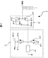
図6は、実施例2によるY駆動部の要部を模式的に示した回路構成図である。なお、図3と同一な機能を有する要素には同一な符号を付して示し、その反復する説明を省略する。 FIG. 6 is a circuit configuration diagram schematically illustrating a main part of the Y drive unit according to the second embodiment. Note that elements having the same functions as those in FIG. 3 are denoted by the same reference numerals, and repeated description thereof is omitted.
本実施例では、図6に示すように、Y駆動部6Aは、Yサステイン回路61と、スキャン回路63Aとからなる。
In this embodiment, as shown in FIG. 6, the
スキャン回路63Aは、図3で述べたスキャン機能に加え、重畳パルス生成機能を備えている。そのため、スキャン用のフローティング電源PW638と、重畳パルス生成用のフローティング電源PW648とを有し、更に、これらを切り替えるスイッチSW641とSW642とを有している。すなわち、スキャンパルス生成の場合には、SW641を閉じて、仮想GNDに対して電源電圧Vscanを有する電源PW638を用い、スキャンパルス(図示せず)を生成し、PDP1に供給する。また、重畳パルス生成の場合には、SW642を閉じて、仮想GNDに対して電源電圧Vdifを有する電源PW648を用い、図3の重畳パルス生成回路と同様に、各出力トランジスタ(例えば、Q631,Q632,D631,D632)を制御して、重畳パルスを生成し、Yサステイン回路61で生成したベースパルスの前縁部に加算(重畳)し、PDP1に供給する。
The
なお、電圧Vdifと電圧Vscanとを同一にできる場合には、フローティング電源を統合し、一つのフローティング電源で、スキャンパルスおよび重畳パルスを生成するようにしてもよい。 When the voltage Vdif and the voltage Vscan can be made the same, the floating power sources may be integrated and the scan pulse and the superimposed pulse may be generated with one floating power source.
1…PDP、2F…前面板、2R…背面板、3…Y電極、4…X電極、5…A電極、6…Y駆動部、7…X駆動部、8…タイミング制御部、9…画像処理部、10…アドレス駆動部、61…Yサステイン回路、62…Y重畳パルス生成回路、63…スキャン回路、71…Xサステイン回路、72…X重畳パルス生成回路、81…ベースパルス制御信号、82…重畳パルス制御信号、83…スキャン制御信号、85…A電極制御信号、616…電力回収回路、Q611,612…トランジスタ、D611,612…ダイオード、PW618…電源、Q621,622…トランジスタ、D621,622…ダイオード、PW628…電源、Q631〜634…トランジスタ、D631〜634…ダイオード、PW638…電源、716…電力回収回路、Q711,712…トランジスタ、D711,712…ダイオード、PW718…電源、Q721,722…トランジスタ、D721,722…ダイオード、PW728…電源、
DESCRIPTION OF
Claims (5)
対を成す維持電極間に所定の時間間隔で交互に極性の異なる駆動電圧を印加して維持放電を行うAC型プラズマディスプレイパネルと、
維持放電期間に前記AC型プラズマディスプレイパネルを交互に駆動するための駆動電圧を前記維持電極に印加する維持放電駆動回路とを備え、
前記維持放電駆動回路が出力する駆動電圧の波形は、第1電圧パルスと、第2電圧パルスとを含み、
前記第1電圧パルスは、前記維持放電を開始させるための第1電圧と、第1パルス幅を有し、
前記第2電圧パルスは、前記第1電圧よりも低く、前記維持放電を停止させるための第2電圧と、前記第1パルス幅よりも大きい第2パルス幅を有し、
前記維持放電駆動回路は、前記第2電圧を有し、かつ前記第1パルス幅と第2パルス幅との合計に対応するベースパルス発生するベースパルス発生部と、
前記第1電圧レベルと前記第2電圧との差に対応する電圧を有し、かつ前記第1パルス幅の重畳パルスを生成し、前記ベースパルスの前縁部に前記重畳パルスを重畳する重畳パルス生成部と、を含むことを特徴とするプラズマディスプレイ装置。 In the plasma display device,
An AC type plasma display panel that performs sustain discharge by alternately applying drive voltages having different polarities at predetermined time intervals between the pair of sustain electrodes;
A sustain discharge drive circuit for applying a drive voltage for alternately driving the AC type plasma display panel to the sustain electrodes during a sustain discharge period;
The waveform of the driving voltage output from the sustain discharge driving circuit includes a first voltage pulse and a second voltage pulse,
The first voltage pulse has a first voltage for starting the sustain discharge and a first pulse width,
The second voltage pulse has a second voltage lower than the first voltage, the second voltage for stopping the sustain discharge, and a second pulse width larger than the first pulse width;
The sustain discharge drive circuit has the second voltage and generates a base pulse corresponding to the sum of the first pulse width and the second pulse width;
A superimposed pulse having a voltage corresponding to a difference between the first voltage level and the second voltage, generating a superimposed pulse having the first pulse width, and superimposing the superimposed pulse on a leading edge of the base pulse A plasma display device comprising: a generation unit;
Priority Applications (2)
| Application Number | Priority Date | Filing Date | Title |
|---|---|---|---|
| JP2006348744A JP2008158366A (en) | 2006-12-26 | 2006-12-26 | Plasma display device |
| US11/896,475 US20080150837A1 (en) | 2006-12-26 | 2007-08-31 | Plasma display apparatus |
Applications Claiming Priority (1)
| Application Number | Priority Date | Filing Date | Title |
|---|---|---|---|
| JP2006348744A JP2008158366A (en) | 2006-12-26 | 2006-12-26 | Plasma display device |
Publications (1)
| Publication Number | Publication Date |
|---|---|
| JP2008158366A true JP2008158366A (en) | 2008-07-10 |
Family
ID=39542051
Family Applications (1)
| Application Number | Title | Priority Date | Filing Date |
|---|---|---|---|
| JP2006348744A Pending JP2008158366A (en) | 2006-12-26 | 2006-12-26 | Plasma display device |
Country Status (2)
| Country | Link |
|---|---|
| US (1) | US20080150837A1 (en) |
| JP (1) | JP2008158366A (en) |
Family Cites Families (3)
| Publication number | Priority date | Publication date | Assignee | Title |
|---|---|---|---|---|
| WO1999018561A1 (en) * | 1997-10-06 | 1999-04-15 | Technology Trade And Transfer Corporation | Method of driving ac discharge display |
| JP3039500B2 (en) * | 1998-01-13 | 2000-05-08 | 日本電気株式会社 | Driving method of plasma display panel |
| TW507237B (en) * | 2000-03-13 | 2002-10-21 | Panasonic Co Ltd | Panel display apparatus and method for driving a gas discharge panel |
-
2006
- 2006-12-26 JP JP2006348744A patent/JP2008158366A/en active Pending
-
2007
- 2007-08-31 US US11/896,475 patent/US20080150837A1/en not_active Abandoned
Also Published As
| Publication number | Publication date |
|---|---|
| US20080150837A1 (en) | 2008-06-26 |
Similar Documents
| Publication | Publication Date | Title |
|---|---|---|
| JP2001013917A (en) | Display device | |
| JP4204054B2 (en) | Driving method and driving apparatus for plasma display panel | |
| US7492333B2 (en) | Plasma display device and driving method thereof | |
| JP2776298B2 (en) | Driving circuit and driving method for capacitive load | |
| JP2008158366A (en) | Plasma display device | |
| US20060050020A1 (en) | Plasma display apparatus and driving method thereof | |
| US20080136744A1 (en) | Plasma Display Device and Power Supply Module | |
| TW200425010A (en) | Display panel driving method | |
| CN101599246B (en) | Plasma display and method for driving plasma display panel | |
| JP2006146215A (en) | Plasma display device and driving method thereof | |
| CN101276537A (en) | Plasma display panel driving circuit device and plasma display device | |
| JPWO2008084792A1 (en) | Plasma display device | |
| CN100430978C (en) | Driving circuit, method and system for flat display device | |
| KR101046815B1 (en) | Plasma display device | |
| JP2007507730A (en) | Driving device for plasma display panel | |
| JP2005025201A (en) | Method of generating short-duration pulses on a plurality of columns or rows of a plasma display and device for implementing method | |
| US20060208966A1 (en) | Drive circuit and plasma display device | |
| KR100625543B1 (en) | Driving device of plasma display panel driven by low reset voltage | |
| JP2005221796A (en) | Plasma display apparatus and plasma display driving method | |
| KR100649528B1 (en) | Plasma Display and Driving Device | |
| US20080068366A1 (en) | Plasma display, and driving device and method thereof | |
| JP2009122649A (en) | Plasma display device and driving device and driving method thereof | |
| KR100741780B1 (en) | Plasma Display Panel Driving Device | |
| JP2009122169A (en) | Drive circuit | |
| JP2007108627A (en) | Plasma display device |