JP2008158285A - Image display device - Google Patents
Image display device Download PDFInfo
- Publication number
- JP2008158285A JP2008158285A JP2006347332A JP2006347332A JP2008158285A JP 2008158285 A JP2008158285 A JP 2008158285A JP 2006347332 A JP2006347332 A JP 2006347332A JP 2006347332 A JP2006347332 A JP 2006347332A JP 2008158285 A JP2008158285 A JP 2008158285A
- Authority
- JP
- Japan
- Prior art keywords
- circuit
- correction
- signal
- pixel
- luminance
- Prior art date
- Legal status (The legal status is an assumption and is not a legal conclusion. Google has not performed a legal analysis and makes no representation as to the accuracy of the status listed.)
- Withdrawn
Links
Images


Classifications
-
- G—PHYSICS
- G09—EDUCATION; CRYPTOGRAPHY; DISPLAY; ADVERTISING; SEALS
- G09G—ARRANGEMENTS OR CIRCUITS FOR CONTROL OF INDICATING DEVICES USING STATIC MEANS TO PRESENT VARIABLE INFORMATION
- G09G3/00—Control arrangements or circuits, of interest only in connection with visual indicators other than cathode-ray tubes
- G09G3/20—Control arrangements or circuits, of interest only in connection with visual indicators other than cathode-ray tubes for presentation of an assembly of a number of characters, e.g. a page, by composing the assembly by combination of individual elements arranged in a matrix no fixed position being assigned to or needed to be assigned to the individual characters or partial characters
- G09G3/22—Control arrangements or circuits, of interest only in connection with visual indicators other than cathode-ray tubes for presentation of an assembly of a number of characters, e.g. a page, by composing the assembly by combination of individual elements arranged in a matrix no fixed position being assigned to or needed to be assigned to the individual characters or partial characters using controlled light sources
-
- G—PHYSICS
- G09—EDUCATION; CRYPTOGRAPHY; DISPLAY; ADVERTISING; SEALS
- G09G—ARRANGEMENTS OR CIRCUITS FOR CONTROL OF INDICATING DEVICES USING STATIC MEANS TO PRESENT VARIABLE INFORMATION
- G09G2310/00—Command of the display device
- G09G2310/02—Addressing, scanning or driving the display screen or processing steps related thereto
- G09G2310/0264—Details of driving circuits
- G09G2310/0275—Details of drivers for data electrodes, other than drivers for liquid crystal, plasma or OLED displays, not related to handling digital grey scale data or to communication of data to the pixels by means of a current
-
- G—PHYSICS
- G09—EDUCATION; CRYPTOGRAPHY; DISPLAY; ADVERTISING; SEALS
- G09G—ARRANGEMENTS OR CIRCUITS FOR CONTROL OF INDICATING DEVICES USING STATIC MEANS TO PRESENT VARIABLE INFORMATION
- G09G2320/00—Control of display operating conditions
- G09G2320/02—Improving the quality of display appearance
- G09G2320/0233—Improving the luminance or brightness uniformity across the screen
-
- G—PHYSICS
- G09—EDUCATION; CRYPTOGRAPHY; DISPLAY; ADVERTISING; SEALS
- G09G—ARRANGEMENTS OR CIRCUITS FOR CONTROL OF INDICATING DEVICES USING STATIC MEANS TO PRESENT VARIABLE INFORMATION
- G09G2320/00—Control of display operating conditions
- G09G2320/02—Improving the quality of display appearance
- G09G2320/0285—Improving the quality of display appearance using tables for spatial correction of display data
Landscapes
- Engineering & Computer Science (AREA)
- Physics & Mathematics (AREA)
- Computer Hardware Design (AREA)
- General Physics & Mathematics (AREA)
- Theoretical Computer Science (AREA)
- Control Of Indicators Other Than Cathode Ray Tubes (AREA)
Abstract
Description
本発明は、画像表示装置に関する。 The present invention relates to an image display device.
特許文献1(特開2000−75833号公報)は、ディスプレイにおける蛍光体のγ特性を考慮し、輝度信号と色信号について、原画像信号の色彩と明暗を忠実に画像表示装置に表示するためのガンマ補正として蛍光体飽和補正方法を開示する。 Patent Document 1 (Japanese Patent Laid-Open No. 2000-75833) considers the γ characteristic of a phosphor in a display, and displays the color and brightness of an original image signal faithfully on an image display device for a luminance signal and a color signal. A phosphor saturation correction method is disclosed as gamma correction.
特許文献2(米国特許第6、307、327号明細書)は、電界放出ディスプレイにおけるスペーサの可視性を制御する方法として、スペーサ近傍の第1領域と、スペーサ非近傍の第2領域に領域を定義し、スペーサを視者に対して見えなくするために、スペーサ近傍の第1領域の複数画素によって発生する光の強度レベルに応じて第1領域に伝送する画素データを修正するという画素データ補正方法を開示する。 Patent Document 2 (US Pat. No. 6,307,327) discloses a method for controlling the visibility of a spacer in a field emission display by arranging regions in a first region near the spacer and a second region near the spacer. Pixel data correction that corrects pixel data to be transmitted to the first area according to the intensity level of light generated by a plurality of pixels in the first area near the spacer in order to define and make the spacer invisible to the viewer A method is disclosed.
特許文献3(特開2005−301218号公報)は、補正量が、補正対象蛍光体周辺に位置する各蛍光体の駆動状態を反映した値であり、かつ、入力信号と蛍光体の表示との間の非線形特性に応じた調整が補正対象蛍光体に対応する入力信号の値に基づいて行われた値であることを開示する。 In Patent Document 3 (Japanese Patent Laid-Open No. 2005-301218), the correction amount is a value reflecting the driving state of each phosphor located around the correction target phosphor, and the input signal and the phosphor display are It is disclosed that the adjustment according to the non-linear characteristic is a value made based on the value of the input signal corresponding to the correction target phosphor.
特許文献4(特開2006−195444号公報)は、スペーサを視者に対して見えなくする為の補正する時に、R、G、B蛍光体毎に補正量を変化させ、点灯状況によっても最適補正量を変化させることを開示する。
画像表示装置においては、より好ましい画像表示を実現できる構成が望まれている。より望ましい画像表示とは例えばむらの少ない画像表示である。 In an image display device, a configuration capable of realizing a more preferable image display is desired. More desirable image display is, for example, image display with less unevenness.
まず、ビームとハレーションについて説明する。電子源から放出された電子が、蛍光体に衝突するとビームが発生する。そしてこの時ビームを発生させるだけでなく、弾性散乱が起こる(図15)。なお、ビーム輝度とは、蛍光体内で点灯しているビームのみによる輝度のことを示しており、後方散乱電子による発光は含めていない(図15)。そして弾性散乱により周辺に飛び散った後方散乱電子が周辺の蛍光体を発光させ、その発光のことをハレーションと呼んでいる。 First, beams and halation will be described. When electrons emitted from the electron source collide with the phosphor, a beam is generated. At this time, not only the beam is generated but also elastic scattering occurs (FIG. 15). Note that the beam luminance indicates the luminance due to only the lighted beam in the phosphor, and does not include light emission due to backscattered electrons (FIG. 15). The backscattered electrons scattered around by the elastic scattering cause the surrounding phosphors to emit light, and this light emission is called halation.
本発明者は、点灯蛍光体と非点灯蛍光体では、それぞれに後方散乱電子が同量付加された場合に生じる発光増加分は、それぞれ異なることを発見した(図16)。図16(a)のように周辺蛍光体を点灯させると、後方散乱電子量は対象蛍光体内にほぼ均一に分布する(図16(c))。しかし、同一蛍光体内のビーム点灯箇所と非点灯箇所でのハレーシ
ョン発光分を比較すると、点灯箇所では非点灯箇所よりハレーションが少ないことが判明した((図16(b))。このことにより、補正対象蛍光体の点灯状況によって、スペー
サむらが変化し、最適な補正量も変化することが判明した。
The present inventor has found that the increase in emission generated when the same amount of backscattered electrons is added to each of the lit phosphor and the non-lit phosphor is different (FIG. 16). When the peripheral phosphor is turned on as shown in FIG. 16A, the amount of backscattered electrons is almost uniformly distributed in the target phosphor (FIG. 16C). However, a comparison of the amount of halation light emission at the beam-lit and non-lighted locations within the same phosphor revealed that there was less halation at the illuminated locations than at the non-lit locations (FIG. 16 (b)). It has been found that the unevenness of the spacer changes and the optimum correction amount also changes depending on the lighting state of the target phosphor.
本発明者は、任意のビームの輝度と、ハレーション輝度の比率がこのビーム輝度に対し常に一定というわけではなく、図4、図5のハレーション補正部の入力値の変動に対応して変化していることを実験より発見した(図13)。この原因を細かく調べると、蛍光体の輝度―電荷量の関係は点灯ビームのような高電荷領域ではγ≠1であるが、ハレーションのような低電荷領域ではγ≒1であるからということがわかった(図14)。そのことにより、補正する画素周辺の画素の点灯状況によって、スペーサむらの比率等が変化する。従来の補正方法では、上述の蛍光体の輝度―電荷量の関係が考慮されていなかった。 The present inventor does not always say that the ratio of the luminance of the arbitrary beam and the halation luminance is constant with respect to the beam luminance, but changes in accordance with the fluctuation of the input value of the halation correction unit in FIGS. It was discovered by experiment (FIG. 13). Examining the cause in detail, the relationship between the luminance and the charge amount of the phosphor is γ ≠ 1 in a high charge region such as a lighting beam, but γ≈1 in a low charge region such as halation. Okay (Figure 14). As a result, the spacer unevenness ratio or the like changes depending on the lighting conditions of the pixels around the pixel to be corrected. In the conventional correction method, the above-described relationship between the luminance and the charge amount of the phosphor has not been considered.
本発明の目的は、高精度に表示むらの補正ができる画像表示装置を提供することにある。 An object of the present invention is to provide an image display device capable of correcting display unevenness with high accuracy.
本発明は上記目的を達成するため、対応付けられた所定の発光領域をそれぞれ有し、該発光領域を発光させることによって画像を表示する複数の表示素子と、所定の発光領域以外の発光領域に対応する表示素子を駆動することに起因して該所定の発光領域が発光するのを抑制するスペーサと、入力された画像データに基づいて、表示素子を駆動する駆動信号を出力する駆動回路と、を有し、駆動回路は、入力された画像データを輝度に対してリニアな信号に近づける補正をすることにより輝度信号を得る第1の補正回路と、補正された駆動信号を出力するための第2の補正回路と、を有し、該第2の補正回路は、入力された画像データによる所定の発光領域の発光に対して、該所定の発光領域以外の発光領域に対応する表示素子の駆動が与える影響をスペーサが抑制する抑制効果を評価した評価値を算出する算出回路と、調整回路と、を有し、算出回路は、輝度信号を電荷量に対してリニアな信号に近づける補正をすることにより、輝度信号が指定する輝度を得るために必要な電荷量を示す電荷信号に変換した後、電荷信号を用いて抑制効果を評価した評価値を算出し、調整回路は、輝度信号に基づき表示素子の蛍光体の特性を参照した調整値を算出し、評価値と調整値とによって駆動信号に対応する補正値を動的に算出する回路であることを特徴とする。 In order to achieve the above-described object, the present invention has a plurality of display elements each having a predetermined light emitting area associated therewith and displaying an image by emitting light from the light emitting area, and light emitting areas other than the predetermined light emitting areas. A spacer that suppresses light emission of the predetermined light emitting region due to driving of the corresponding display element; a drive circuit that outputs a drive signal for driving the display element based on the input image data; And a driving circuit for correcting the input image data so as to approximate a linear signal with respect to the luminance to obtain a luminance signal, and a first correcting circuit for outputting the corrected driving signal. The second correction circuit drives a display element corresponding to a light emitting area other than the predetermined light emitting area with respect to light emission of the predetermined light emitting area by the input image data. Give A calculation circuit that calculates an evaluation value that evaluates the suppression effect that the spacer suppresses the influence; and an adjustment circuit, and the calculation circuit corrects the luminance signal to be a signal that is linear with respect to the charge amount. After the conversion to a charge signal indicating the amount of charge necessary to obtain the luminance specified by the luminance signal, an evaluation value that evaluates the suppression effect using the charge signal is calculated, and the adjustment circuit displays the display element based on the luminance signal. It is a circuit that calculates an adjustment value with reference to the characteristics of the phosphor and dynamically calculates a correction value corresponding to the drive signal based on the evaluation value and the adjustment value.
また、本発明は、対応付けられた所定の発光領域をそれぞれ有し、該発光領域を発光させることによって画像を表示する複数の表示素子と、所定の発光領域以外の発光領域に対応する表示素子を駆動することに起因して該所定の発光領域が発光するのを抑制するスペーサと、入力された画像データに基づいて、表示素子を駆動する駆動信号を出力する駆動回路と、を有し、駆動回路は、入力された画像データを電荷量に対してリニアな信号に近づける補正をすることにより電荷信号を得る第1の補正回路と、補正された駆動信号を出力するための第2の補正回路と、を有し、該第2の補正回路は、入力された画像データによる所定の発光領域の発光に対して、該所定の発光領域以外の発光領域に対応する表示素子の駆動が与える影響をスペーサが抑制する抑制効果を評価した評価値を算出する算出回路と、調整回路と、を有し、算出回路は、電荷信号を用いて抑制効果を評価した評価値を算出し、調整回路は、電荷信号を輝度に対してリニアな信号に近づける補正をすることにより輝度信号に変換し、輝度信号に基づき表示素子の蛍光体の特性を参照した調整値を算出し、評価値と調整値とによって駆動信号に対応する補正値を動的に算出する回路であることを特徴とする。 The present invention also includes a plurality of display elements each having a predetermined light emitting area associated therewith and displaying an image by causing the light emitting area to emit light, and a display element corresponding to a light emitting area other than the predetermined light emitting area. A spacer that suppresses light emission from the predetermined light-emitting region due to driving, and a drive circuit that outputs a drive signal for driving the display element based on the input image data, The drive circuit includes a first correction circuit that obtains a charge signal by correcting the input image data so as to approximate a linear signal with respect to the charge amount, and a second correction for outputting the corrected drive signal. The second correction circuit affects the light emission of the predetermined light emitting area by the input image data by the drive of the display element corresponding to the light emitting area other than the predetermined light emitting area. Space A calculation circuit that calculates an evaluation value that evaluates the suppression effect that suppresses, and an adjustment circuit. The calculation circuit calculates an evaluation value that evaluates the suppression effect using the charge signal, and the adjustment circuit The signal is converted into a luminance signal by correcting it to be a linear signal with respect to the luminance, and an adjustment value is calculated based on the luminance signal with reference to the characteristics of the phosphor of the display element, and driven by the evaluation value and the adjustment value. It is a circuit that dynamically calculates a correction value corresponding to a signal.
また、本発明は、電子放出素子と、該電子放出素子が放出する電子が入射されることで発光する発光領域とをそれぞれが有する複数の画素と、電子放出素子と発光領域との間の空間を維持するスペーサと、映像信号を変換する第1の変換回路と、第1の変換回路の出力を変換する第2の変換回路と、該第2の変換回路の出力に基づいて補正値を算出する算出回路と、補正値を第1の変換回路の出力に基づいて調整し、調整した補正値を出力する調整回路と、第1の変換回路の出力を調整した補正値で補正する補正回路と、を有し、第1の変換回路は、該第1の変換回路の出力と表示すべき輝度との線形性が映像信号と表示すべき輝度との線形性よりも高くなる変換を行う回路であり、第2の変換回路は、該第2
の変換回路の出力と放出すべき電子量との線形性が第1の変換回路の出力と放出すべき電子量との線形性よりも高くなる変換を行う回路であり、 スペーサは、第1の画素から第2の画素の発光領域に向かう電子を遮蔽する位置に位置しており、算出回路は、第2の画素に対応する補正値を、第2の変換回路の出力の内の第1の画素に対応する出力に基づいて算出するものであり、補正値は、該補正値を用いた補正によって、第2の画素の輝度と該第2の画素よりもスペーサから離れて位置する画素の輝度との差を減少することができる値を有する、ことを特徴とする。
The present invention also provides a plurality of pixels each having an electron-emitting device, a light-emitting region that emits light when electrons emitted from the electron-emitting device are incident, and a space between the electron-emitting device and the light-emitting region. The first conversion circuit that converts the video signal, the second conversion circuit that converts the output of the first conversion circuit, and the correction value is calculated based on the output of the second conversion circuit A correction circuit that adjusts the correction value based on the output of the first conversion circuit, outputs the adjusted correction value, and a correction circuit that corrects the output of the first conversion circuit with the adjusted correction value The first conversion circuit is a circuit that performs conversion in which the linearity between the output of the first conversion circuit and the luminance to be displayed is higher than the linearity between the video signal and the luminance to be displayed. And the second conversion circuit includes the second conversion circuit.
The circuit for performing the conversion in which the linearity between the output of the first conversion circuit and the amount of electrons to be emitted is higher than the linearity between the output of the first conversion circuit and the amount of electrons to be emitted. The calculation circuit is located at a position where electrons from the pixel toward the light emitting region of the second pixel are shielded, and the calculation circuit calculates a correction value corresponding to the second pixel from the first of the outputs of the second conversion circuit. The correction value is calculated based on the output corresponding to the pixel, and the correction value is obtained by correcting using the correction value, the luminance of the second pixel and the luminance of the pixel located farther from the spacer than the second pixel. It has a value that can reduce the difference between and.
また、本発明は、電子放出素子と、該電子放出素子が放出する電子が入射されることで発光する発光領域とをそれぞれが有する複数の画素と、映像信号を変換する第1の変換回路と、第1の変換回路の出力を変換する第2の変換回路と、該第2の変換回路の出力に基づいて補正値を算出する算出回路と、補正値を第1の変換回路の出力に基づいて調整し、調整した補正値を出力する調整回路と、第1の変換回路の出力を調整した補正値で補正する補正回路と、を有し、第1の変換回路は、該第1の変換回路の出力と表示すべき輝度との線形性が映像信号と表示すべき輝度との線形性よりも高くなる変換を行う回路であり、第2の変換回路は、該第2の変換回路の出力と放出すべき電子量との線形性が第1の変換回路の出力と放出すべき電子量との線形性よりも高くなる変換を行う回路であり、複数の画素は第1の画素と該第1の画素の近傍に位置する第2の画素を含んでおり、第1の画素と第2の画素との距離は、第1の画素からでてくる電子が第2の画素に到達する距離であり、算出回路は、第2の画素に対応する補正値を、第2の変換回路の出力の内の第1の画素に対応する出力に基づいて算出するものであり、第1の画素から出てくる電子によって生じる第2の画素の発光、による第2の画素の輝度の増加を補正することができる値を補正値が有する、ことを特徴とする。 The present invention also provides a plurality of pixels each having an electron-emitting device, a light-emitting region that emits light when an electron emitted from the electron-emitting device is incident, and a first conversion circuit that converts a video signal. A second conversion circuit for converting the output of the first conversion circuit; a calculation circuit for calculating a correction value based on the output of the second conversion circuit; and a correction value based on the output of the first conversion circuit. And an adjustment circuit that outputs the adjusted correction value, and a correction circuit that corrects the output of the first conversion circuit with the adjusted correction value. The first conversion circuit includes the first conversion circuit. A circuit that performs conversion in which the linearity between the output of the circuit and the luminance to be displayed is higher than the linearity between the video signal and the luminance to be displayed, and the second conversion circuit outputs the output of the second conversion circuit. And the amount of electrons to be emitted is the output of the first conversion circuit and the amount of electrons to be emitted A plurality of pixels including a first pixel and a second pixel located in the vicinity of the first pixel, and the first pixel and the second pixel. The distance to the pixel is the distance that electrons from the first pixel reach the second pixel, and the calculation circuit calculates the correction value corresponding to the second pixel as the output of the second conversion circuit. Is calculated on the basis of an output corresponding to the first pixel, and corrects an increase in luminance of the second pixel due to light emission of the second pixel caused by electrons emitted from the first pixel. The correction value has a value that enables the correction.
本発明によれば、高精度に表示むらの補正ができる。 According to the present invention, display unevenness can be corrected with high accuracy.
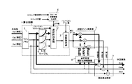
図1は、本実施形態のハレーション補正回路15(本願発明の「第2の補正回路」に相当)である。図4は、本発明に係る駆動回路の構成図である。ハレーション補正回路15は、図4に示すように、蛍光体飽和補正部17の前段に配置されている。
FIG. 1 shows a halation correction circuit 15 (corresponding to a “second correction circuit” of the present invention) of the present embodiment. FIG. 4 is a configuration diagram of a drive circuit according to the present invention. As shown in FIG. 4, the
本実施形態におけるハレーション補正回路15は、図1に示すように、算出回路6と調整ゲイン乗算部5と点灯状況補正比率制御部8とを有する調整回路と補正値加算部7から構成される。算出回路6は、ラインメモリ1、L−Ieテーブル部9、選択的加算部2、係数乗算部3から構成される。
As shown in FIG. 1, the
ラインメモリ1は元画像データを入力する。尚、元画像データは逆γ補正部14により輝度に対してリニアな信号に近づける補正をすることにより得た輝度信号(R、G、B信号)である。ラインメモリ1は補正対象画素に対する周辺参照画素の入力画像信号を出力する。L−Ieテーブル部9は選択的加算部2で周辺参照画素の入力画像信号を電荷量に対してリニアな信号に近づける補正をすることにより電荷信号に変換する。L−Ieテーブル部9は輝度信号が指定する輝度を得るために必要な電荷量を示す電荷信号に変換する。選択的加算部2は電荷信号とSPD値を入力し、補正参照画素の点灯状況を出力する。選
択的加算部2は電荷信号を用いることによりハレーション量を正確に評価することができる。SPD値については後述する。
The
係数乗算部3は補正参照画素の点灯状況とハレーションゲイン値を入力し、抑制効果を評価した評価値(調整前の補正データ)を算出する。調整ゲイン乗算部5は評価値にR,G,B変換係数(本発明の「調整値」に相当)を乗算し、補正対象画素のR,G,B各蛍光体の特性
を参照した補正値を動的に算出する。
The
周辺参照画素とは、補正対象画素周辺の画素のことであり、後方散乱電子が散乱する範囲内の画素のことを示す。 The peripheral reference pixel is a pixel around the correction target pixel, and indicates a pixel within a range where backscattered electrons are scattered.
補正参照画素とは、周辺参照画素のうち、後方散乱電子がスペーサに遮断される画素をいう。スペーサ遮断については後述する。 A corrected reference pixel is a pixel in which backscattered electrons are blocked by a spacer among peripheral reference pixels. The spacer blocking will be described later.
ハレーションゲイン値とは、加算結果を遮断されたハレーション分に変換する係数のことである。 The halation gain value is a coefficient for converting the addition result into the blocked halation.
ここで、ハレーションについて説明する。 Here, the halation will be described.
ハレーションはビーム位置を中心に円形状にほぼ均一で広がる。この為、点灯色以外の色の蛍光体も発光させてしまう。その為、ハレーションは白(R、G、B)発光であり、単色などの画像信号を送っている場合には混色を生じてさせている。 The halation spreads almost uniformly in a circular shape around the beam position. For this reason, phosphors of colors other than the lighting color also emit light. Therefore, halation is white (R, G, B) light emission, and color mixing occurs when an image signal such as a single color is sent.
また、後方散乱電子はスペーサによって遮られる場合、その遮断分はハレーションには寄与していない。その結果、スペーサ近傍と非近傍領域ではそのハレーションによる発光量に差が生じ、特に空間周波数の少ない画像を出力した場合にはスペーサ近傍に輝度むら、色むら(表示むら)を生じさせている。 Further, when backscattered electrons are blocked by the spacer, the blocked amount does not contribute to halation. As a result, there is a difference in the amount of light emission due to the halation between the vicinity of the spacer and the non-near area, and particularly when an image with a low spatial frequency is output, uneven brightness and uneven color (display unevenness) are generated in the vicinity of the spacer.
次に、ハレーション補正について説明する。 Next, the halation correction will be described.
ハレーション補正は、スペーサ遮断分のハレーションを算出し、発光量が不足しているスペーサ近傍の蛍光体に、遮断分の発光量を付加することでむらを目立たなくしようとする補正方法である。 The halation correction is a correction method in which the non-uniformity is made inconspicuous by calculating the halation for spacer blocking and adding the light emission for blocking to a phosphor near the spacer where the light emission is insufficient.
ハレーションのスペーサ遮断分を見積もる時に、補正対象画素の位置に対し、スペーサの反対側でかつハレーション分布範囲内の画素(補正参照画素)を使用する。 When estimating the cutoff of the halation spacer, a pixel (correction reference pixel) on the opposite side of the spacer from the position of the correction target pixel and within the halation distribution range is used.
ハレーション分布範囲というのは同パネルでほぼ一定であるので、補正対象画素とスペーサの距離がわかれば、補正参照画素の位置と数は見積もれる。 Since the halation distribution range is almost constant in the panel, the position and number of correction reference pixels can be estimated if the distance between the correction target pixel and the spacer is known.
スペーサ位置情報生成部4は、スペーサ近傍の補正対象画素に対する補正参照画素の位置をSPD値として保存している。
The spacer position
ラインメモリ1は、周辺参照画素への入力画像信号を収集する。入力画像信号をハレーション量が算出できる形式(電荷信号)に変換する処理を行った後、選択的加算部2はSPD値による補正参照画素の点灯状況のみを合計する。
The
この中間に入る変換処理(L−Ieテーブル処理)は、ハレーション補正15と蛍光体飽和補正17との前後関係により変化する。この処理の詳細は後述する。
This intermediate conversion process (L-Ie table process) changes depending on the relationship between the
選択的加算部2での処理により、スペーサによって遮断されるハレーションを発生させるビームの点灯合計値が見積もれる。係数乗算部3は点灯合計値にハレーションゲイン値を乗算することによって、スペーサ遮断によって生じるハレーションむら量(評価値)を算出する。この評価値にR,G,B変換係数を乗算し、補正対象画素の入力信号に対する補正
値としている。
By the processing in the
<調整回路>
点灯状況補正比率制御部8は、補正対象画素の入力画像信号(輝度信号)を入力する。点灯状況補正比率制御部8は、この入力画像信号に基づきR,G,B変換係数を算出する。こ
の変換係数は、図1、図2に示す係数乗算部3の出力の評価値から、補正対象画素の蛍光体種類に応じて最適な補正値に変換する係数(本発明の「調整値」に相当)である。
<Adjustment circuit>
The lighting state correction
点灯状況補正比率制御部8は、評価値を補正対象画素に対応した補正値に調整する機能を有する。
The lighting state correction
本発明者の検証の結果、点灯画素と非点灯画素では、同量の後方散乱電子が付加されたとしても、その電荷による発光量は異なるということが判明した(図16)。 As a result of the inventor's verification, it has been found that even if the same amount of backscattered electrons is added, the light emission amount due to the charge is different between the lit pixel and the non-lit pixel (FIG. 16).
そこで、蛍光体に対応する画像信号を変動させた時、そこに付加されるハレーションの発光効率を計測し、入力画像信号の変化に対するスペーサむらの輝度量を見積もった。ハレーションの発光効率とは、後方散乱電子量とそれによって発光するハレーション輝度との比率のことである。発光効率の算出方法としては、図16を使用して説明する。 Therefore, when the image signal corresponding to the phosphor was changed, the luminous efficiency of the halation added thereto was measured, and the brightness of the spacer unevenness with respect to the change of the input image signal was estimated. The light emission efficiency of halation is the ratio of the amount of backscattered electrons and the halation luminance emitted thereby. A method for calculating the luminous efficiency will be described with reference to FIG.
<発光効率の算出方法>
まず、補正する対象パネルの一つの画素を計測対象にし、その周辺参照画素は点滅させておく(図16(a))。そして、補正対象画素の点灯状況を変化させながら、周辺参照画素の点滅によるハレーションの増加を計測する。図16におけるハレーション輝度B(補正対象画素は非点灯)を1としたときのハレーション輝度Aの値が発光効率である。ハレーション輝度Aの発光効率は、次のように求めることができる、始めに、周辺参照画素を非点灯且つ補正対象画素を点灯した状態で輝度a1を測定する。次に、周辺参照画素を点灯且つ補正対象画素を点灯した状態で輝度a2を測定する。ハレーション輝度Aは、A=a2−a1で求まる。そして、発光効率は、A/Bで求まる。
<Calculation method of luminous efficiency>
First, one pixel of the target panel to be corrected is set as a measurement target, and its peripheral reference pixel is blinked (FIG. 16A). Then, an increase in halation due to blinking of the peripheral reference pixel is measured while changing the lighting state of the correction target pixel. The value of the halation luminance A when the halation luminance B (correction target pixel is not lit) in FIG. The luminous efficiency of the halation luminance A can be obtained as follows. First, the luminance a1 is measured in a state where the peripheral reference pixel is not lit and the correction target pixel is lit. Next, the luminance a2 is measured with the peripheral reference pixels turned on and the correction target pixels turned on. The halation luminance A is obtained by A = a2-a1. The luminous efficiency is obtained by A / B.
実際には、補正対象画素よりも先に駆動されるラインの周辺参照画素からのハレーション電子は、補正対象画素の蛍光体が未励起の状態で入射され、補正対象画素よりも後に駆動されるラインの周辺参照画素からのハレーション電子は、補正対象画素の蛍光体が励起された状態で入射される。従って、より厳密には、スペーサと補正対象画素との関係に応じて変換係数を最適化することが望ましい。 Actually, the halation electrons from the peripheral reference pixels of the line driven before the correction target pixel are incident on the phosphor of the correction target pixel in an unexcited state, and are driven after the correction target pixel. The halation electrons from the peripheral reference pixels are incident in a state where the phosphor of the correction target pixel is excited. Therefore, more strictly, it is desirable to optimize the conversion coefficient in accordance with the relationship between the spacer and the correction target pixel.
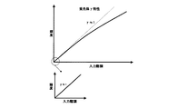
これを補正対象画素の入力階調ごとに示したものの一例が図11に示すグラフ(点灯状況補正比率制御テーブル)である。この発光効率の変化(蛍光体の特性)が評価値を最適な補正値に変換する変換係数(調整値)を表している。この変換係数を点灯状況補正比率制御部8に組み込むことで、評価値を最適な補正量に変換することが出来る。
An example showing this for each input gradation of the correction target pixel is a graph (lighting condition correction ratio control table) shown in FIG. This change in luminous efficiency (phosphor characteristics) represents a conversion coefficient (adjustment value) for converting the evaluation value into an optimum correction value. By incorporating this conversion coefficient into the lighting condition correction
<L−Ieテーブル部9>
L−Ieテーブル部9では補正対象画素とその周辺参照画素のそれぞれの点灯状況から、むらの量を正確に算出する機能を有する。
<L-
The L-
L−Ieテーブル部9は、ラインメモリ1で読み込まれた各画素の点灯状態を示す輝度信号を入力し、輝度信号を電荷に対してリニアな信号に近づける補正をすることにより、輝度信号が指定する輝度を得るために必要な電荷量を示す電荷信号に変換する。電荷信号を用いることにより、その各蛍光体から発生するハレーション発光量を正確に求めることができる。
The L-
特許文献1(特開2000−75833)においては、蛍光体の発光特性は照射される電子ビームの量に対しては線形(リニア)ではなく、蛍光体の種類や蛍光体に照射される
電子ビームのビーム密度、ビーム照射時間などにより変化することが述べられている。一般に蛍光体の発光特性はビームの照射時間が長い場合や、ビームの強度が強い場合ほど、その発光輝度が低下する現象がある(蛍光体の飽和と呼ぶ)。この現象の存在の為、L−Ieテーブル部9を設けている。同様の理由で、Ie−Lテーブル部11が図2に示す補正比率制御部10に設けられている(図3)。
In Patent Document 1 (Japanese Patent Laid-Open No. 2000-75833), the light emission characteristics of the phosphor are not linear with respect to the amount of the electron beam irradiated, but the type of the phosphor and the electron beam irradiated to the phosphor. It is stated that it varies depending on the beam density, beam irradiation time, and the like. In general, the emission characteristics of phosphors have a phenomenon that the emission luminance decreases as the beam irradiation time is longer or the beam intensity is stronger (referred to as phosphor saturation). Because of this phenomenon, the L-
図4のように蛍光体飽和補正部17がハレーション補正部15より後にくる場合はL−Ieテーブルを図1のように設置する。尚、図5のように蛍光体飽和補正部17がハレーション補正部15より前にくる場合はIe−Lテーブルを図3のように設置する。蛍光体飽和補正17をハレーション補正部15の後段に設置する場合、入力元画像の信号は輝度信号となる(図1)。この輝度信号からハレーションの輝度情報を正確に求める必要がある。そのため、輝度信号をビームの電荷信号に変換する(輝度L→電荷Ie)。その理由は、ビームを発光させる電子の電荷量(ビーム電荷量)とハレーションとの関係はリニアだからである。その為、選択的加算部2の前にL−Ieテーブルを置いて、入力に対するハレーションが換算できる形式(電荷信号)に変換する。輝度信号と、電荷信号に基づいて得た評価値及び調整値ともに未だ蛍光体飽和補正の処理を受けていないので、補正値を輝度信号に加算するだけでよい。
When the phosphor
次に、本L−Ieテーブルの求め方を説明する。 Next, how to obtain this L-Ie table will be described.
まずR、G、Bのガンマ特性を計測し、入力、出力をそれぞれの最大値で規格化する(図6)。これを逆変換し(図8)その後、BIT補正で決定される最大出力位置、および、
その位置におけるR、G、B出力のうちの最大値においてそれぞれ規格化する(図9)。
First, the R, G, and B gamma characteristics are measured, and the input and output are normalized by their maximum values (FIG. 6). This is inversely transformed (FIG. 8), then the maximum output position determined by BIT correction, and
Each of the R, G, and B outputs at that position is normalized at the maximum value (FIG. 9).
BIT補正とは図1の蛍光体飽和補正部17の前段にある処理である。未処理の場合パネ
ルの各蛍光体からの出力にはバラツキが存在している。BIT補正とはそのバラツキを抑え
る為、ある一定の輝度値に最大出力をそろえる手法である。
The BIT correction is a process preceding the phosphor
ここでは一例としてBIT補正の最大輝度の0.7倍にビーム輝度を補正する例を示して
いる。図8のα1とβ1が図9のα2とβ2にそれぞれ対応している。これがL−Ieテーブルである。
Here, as an example, the beam luminance is corrected to 0.7 times the maximum luminance of BIT correction. Α1 and β1 in FIG. 8 correspond to α2 and β2 in FIG. 9, respectively. This is the L-Ie table.
尚、蛍光体飽和補正部17をハレーション補正部15の前段に設置すると、補正対象蛍光体箇所の元画像の信号は電荷に対応した信号(電荷信号)になる(図2)。ハレーション分を見積もる時はハレーション輝度とビーム電荷量は比例することから、そのまま選択的加算部2の処理を行う。補正値を電荷信号に付加する場合は、ビームの電荷信号は既に蛍光体飽和補正が終わっているので、電荷信号に加算する時に補正値は蛍光体飽和補正処理を受けなければならない。そこで図3に示すように、補正比率制御部10にIe−Lテーブル部11を設置する。
If the phosphor
Ie−Lテーブル部11はR、G、Bのガンマ特性を計測し、入力、出力をそれぞれの最大値で規格化(図6)したものを利用する。
The Ie-
<実施例1>
本発明の画像表示装置は、SED表示装置、FED表示装置などを包含しており、自発光した輝点輝度によって周辺参照画素でハレーション発光が生じる可能性があるため本発明が適用される好ましい形態である。
<Example 1>
The image display device of the present invention includes an SED display device, an FED display device, and the like, and a preferred embodiment to which the present invention is applied because there is a possibility that halation light emission may occur in the peripheral reference pixels due to the brightness of the self-luminous bright spot. It is.
このSEDパネルに映像信号を入力し表示するまでの動作を説明する。図4において、信号S1は入力映像信号であり、信号処理部13にて、表示に好適な信号処理が成され、
信号S2が表示信号として出力される。信号処理部13の機能については、本実施形態を説明する上での必要最小限の機能ブロックについて記載している。14は逆γ補正部(本発明の「第1の補正回路」に相当)である。一般的に、入力映像信号S1はCRTディスプレイ装置で表示することを前提として、CRTディスプレイの入力−発光特性に合わせたガンマ変換と呼ばれる0.45乗などの非線形変換が施され、通信回線を介して伝送さ
れるいは記録媒体に記録されている。
The operation until the video signal is input and displayed on the SED panel will be described. In FIG. 4, a signal S1 is an input video signal, and signal processing suitable for display is performed in the
The signal S2 is output as a display signal. The functions of the
逆γ補正部14は、その映像信号を、SED、FED、PDPなどの入力−発光特性がリニアな表示デバイスに表示するため、入力信号に対して、2.2乗などの逆ガンマ変換
を施す。逆γ補正部14の出力データは表示パネルの輝度とデータがリニアな系に変換され、本実施例での特徴部となるハレーション補正部15に入力される。実際には、回路で処理すると真にリニアな信号にならない場合がある。このため、逆γ補正部14は、入力された画像データを輝度に対してリニアな信号に近づける補正をすることにより輝度信号を得ることとなる。ハレーション補正部15に関しては以降で詳しく説明する。BIT補正
部16は、ハレーション補正部15からの出力を入力し、電子源と蛍光体に起因する発光のばらつきをそろえる為に、一定の輝度値に最大輝度をそろえることで隣接のばらつきをそろえる。蛍光体飽和補正部17は、BIT補正部16の出力を入力し、R、G、B蛍光体
ごとのガンマ特性を考慮して、入力に対して出力色彩と明暗を忠実に表示することが出来るように調整する。蛍光体飽和補正部17は、SEDにとって最適な映像の表示信号S2を出力する。タイミング制御部18は、入力映像信号S1と共に受け渡された同期信号を元に、各ブロックの動作のための各種タイミング信号を生成し出力する。
The inverse
19はPWMパルス制御部で、水平1周期(行選択期間)毎に表示信号S2を表示パネル25に適応した駆動信号(例では、PWM変調)に変換する。20は駆動電圧制御部で、表示パネル25に配置されている素子を駆動する電圧を制御する。21は列配線スイッチ部で、トランジスタなどのスイッチ手段により構成され、毎水平1周期(行選択期間)ごとに駆動電圧制御部20からの駆動出力をPWMパルス制御部19から出力されるPWMパルス期間だけパネル列電極に印加する。22は行選択制御部で、表示パネル25上の素子を駆動する行選択パルスを発生する。23は行配線スイッチ部で、トランジスタなどのスイッチ手段により構成され、行選択制御部22から出力される行選択パルスに応じた駆動電圧制御部20駆動出力を表示パネル25に出力する。24は高電圧発生部で、表示パネル25に配置されている電子放出素子から放出された電子を不図示の蛍光体に衝突させるために加速する加速電圧を発生する。以上により、表示パネル25が駆動されて映像が表示される。
A PWM
なお、本発明の駆動回路は、信号処理部13、PWMパルス制御部19、駆動電圧制御部20、列配線スイッチ部21、行選択制御部22、行配線スイッチ部23を含む。
The drive circuit of the present invention includes a
<ハレーション補正部15>
次に、本発明の特徴部であるハレーション補正部15について図1を用いて説明する。
<
Next, the
図17(a)は、リアプレートに形成した電子放出素子と、該電子放出素子と間隔を空けてフェースプレートに配置される発光体(本例では、赤、青、緑の各色の蛍光体)とを用いた画像表示装置である。本発明者は、電子放出素子から放出される電子ビーム(1次電子)を発光体に照射して発光体を発光させる画像表示装置において色再現性が所望の状態とは異なるという特有の課題が生じることを見出した。 FIG. 17A shows an electron-emitting device formed on the rear plate, and a light emitter (in this example, phosphors of red, blue, and green colors) disposed on the face plate at a distance from the electron-emitting device. And an image display device using the above. The inventor has a unique problem that color reproducibility is different from a desired state in an image display device that emits light from a light emitter by irradiating the light emitter with an electron beam (primary electrons) emitted from an electron-emitting device. Found out that it would occur.
具体的な例を挙げると、青の蛍光体にのみ電子を照射して青色の発光を得ようとした場合に、純粋な青ではなく、わずかに他の色すなわち、緑と赤の発光が混ざった発光状態、すなわち、彩度が良くない発光状態になることがわかった。本発明者は研究を重ねた結果
、彩度が低下する原因を確認した。電子放出素子が放出する1次電子が、該電子放出素子が対応する発光体に入射することで、対応する発光体が輝点発光する。これに加えて、上記発光体で反射することで近接(隣接も含む)の異なる色の発光領域に後方散乱電子(反射電子・2次電子)として入射することで周辺の発光体も発光させることを確認した。この後方散乱電子による発光の様に、表示素子が近接する表示素子の駆動による影響を受けて発光する現象を本発明ではハレーションと呼んでいる。SEDにおいては、図17(b
)に示すようにある蛍光体に電子が照射されるとその表示素子を中心にハレーションによる円形発光(発光量としての輝度で表現すると輝点を中心とした円柱形に分布)が起きることが分かった。このハレーションの及ぶ円形領域の半径がn画素であれば、後ほど詳しく説明するハレーション補正処理のための画素参照範囲として2n+1タップのフィルタが必要になる。更に、前記ハレーションの及ぶ領域の半径は、蛍光体が配置されているフェースプレートと電子源が配置されているリアプレートとの間隔、画素サイズなどによって一意に決めても実用上差支えないことが分かった。したがって、フェースプレートとリアプレートの間隔がわかっていれば、フィルタタップ数は一意に決まる。本実施例ではn=5画素であったために、11タップフィルタ、つまり、ハレーションの影響度を考慮する為には、図18示したように11画素×11ラインのデータ参照を行えばよいことが分かる。このようにハレーションの及ぶ領域の半径はパネルの物理構造(フェースプレートとリアプレートとの間隔、画素サイズ)から得られる静的パラメータである。そのため、同一の補正回路を複数の種別の異なるSEDパネルに対応させる場合は、図18のハレーションマスクパターンを可変パラメータとして変更できるようにしておけば良い。
As a specific example, when only blue phosphor is irradiated with electrons to obtain blue light emission, it is not pure blue but slightly mixed with other colors, that is, green and red light emission. It was found that the light emission state, that is, the light emission state with poor saturation was obtained. As a result of repeated research, the present inventor has confirmed the cause of the decrease in saturation. When the primary electrons emitted from the electron-emitting device are incident on the light emitter corresponding to the electron-emitting device, the corresponding light emitter emits bright spots. In addition to this, the surrounding light emitters also emit light by being reflected as backscattered electrons (reflected electrons / secondary electrons) in the light emitting regions of different colors in the vicinity (including adjacent ones) by being reflected by the light emitters. It was confirmed. In the present invention, a phenomenon in which light is emitted under the influence of driving of a display element that is close to the display element, such as light emission by backscattered electrons, is called halation. In the SED, FIG.
As shown in Fig. 3, it is understood that when a phosphor is irradiated with electrons, circular light emission (distribution in a cylindrical shape centered on a bright spot when expressed in terms of luminance as a light emission amount) occurs due to halation centering on the display element. It was. If the radius of the circular area where the halation extends is n pixels, a 2n + 1 tap filter is required as a pixel reference range for the halation correction process described in detail later. Further, it can be seen that the radius of the halation covered area can be practically determined even if it is uniquely determined by the distance between the face plate on which the phosphor is arranged and the rear plate on which the electron source is arranged, the pixel size, and the like. It was. Therefore, if the distance between the face plate and the rear plate is known, the number of filter taps is uniquely determined. In this embodiment, since n = 5 pixels, in order to consider the influence of the 11 tap filter, that is, the halation, the data reference of 11 pixels × 11 lines may be performed as shown in FIG. I understand. As described above, the radius of the halation area is a static parameter obtained from the physical structure of the panel (the distance between the face plate and the rear plate, the pixel size). Therefore, when the same correction circuit is made to correspond to a plurality of different types of SED panels, the halation mask pattern in FIG. 18 may be changed as a variable parameter.
図19は反射電子の反射軌道にスペーサのような遮蔽部材がない場合(スペーサ非近傍)である。スペーサのような遮蔽部材がある場合(スペーサ近傍)は後方散乱電子(反射電子・2次電子)が図17(a)に示すようにスペーサにより遮断されてしまうためハレーション強度が軽減する。よって、スペーサの最近接の電子放出素子から電子ビーム(1次電子)が放出された場合のハレーションの影響範囲は図17(b)のように半円発光となってしまうことが分かった。図19(a)、図17(a)では蛍光体はライン方向にRGB交互<横ストライプ>に配列されているように図示しているが、これは説明を分かりやすくするためであり、実際は水平方向にRGB交互<縦ストライプ>に配列されている。 FIG. 19 shows a case where there is no shielding member such as a spacer in the reflection trajectory of reflected electrons (near the spacer). When there is a shielding member such as a spacer (in the vicinity of the spacer), backscattered electrons (reflected electrons and secondary electrons) are blocked by the spacer as shown in FIG. Therefore, it was found that the range of influence of halation when an electron beam (primary electron) is emitted from the electron emitting element closest to the spacer is semicircular emission as shown in FIG. In FIG. 19A and FIG. 17A, the phosphors are illustrated as being arranged in RGB alternate <horizontal stripes> in the line direction, but this is for ease of explanation, and in fact it is horizontal. It is arranged in RGB direction <vertical stripe> in the direction.
以上の動作は、1表示素子からの発光時を例にして説明したハレーションの発生メカニズムである。本実施形例で用いたSEDには、水平方向に伸びる複数の長尺スペーサが数十ラインおきに実装されている。全面同色点灯をした場合、上述したハレーションによりスペーサ近傍とスペーサ非近傍の異なる領域間でハレーション量の違いが生じ、スペーサ近傍付近は色純度が変化するスペーサむらという特有の課題が生じてしまうことが確認された。スペーサむらの違いは表示画像の点灯パターンにより異なるが、例えば、全面青を点灯した場合、図20(a)に示したように、青の発光輝度にハレーション輝度が付加され、スペーサ近傍はスペーサからの距離依存で、反射電子の遮断量が段階的に変わるため、10ライン程度の幅の段階的なくさび状の色純度の変化が視認される。 The above operation is the halation generation mechanism described by taking the case of light emission from one display element as an example. In the SED used in this embodiment, a plurality of long spacers extending in the horizontal direction are mounted every several tens of lines. When the entire surface is lit in the same color, the halation described above causes a difference in the halation amount between different regions in the vicinity of the spacer and in the vicinity of the non-spacer. confirmed. The difference in the unevenness of the spacer varies depending on the lighting pattern of the display image. For example, when blue is entirely lit, as shown in FIG. 20A, halation luminance is added to the blue emission luminance, and the vicinity of the spacer is Depending on the distance, the amount of reflected electrons blocked changes stepwise, so that a stepwise wedge-like change in color purity with a width of about 10 lines is visually recognized.
本出願者は鋭意努力の末、前述したスペーサむらを引き起こす要因を考慮し、SEDの画質を改善できる新規な画像表示装置の構成及び駆動信号の補正方法を見出した。以下では本願に係る発明の画像表示装置及び駆動信号の補正方法の具体的な例について図1を用いて説明する。 As a result of diligent efforts, the present applicant has found a novel image display device configuration and drive signal correction method that can improve the image quality of the SED in consideration of the above-described factors causing the spacer unevenness. A specific example of the image display device and the drive signal correction method according to the present invention will be described below with reference to FIG.
1はラインメモリで、本実施例では11ラインメモリで構成される。元画像データは、ラインメモリ1にライン単位で順次書き込まれ、11ライン分のデータが格納された時点で演算参照のために11画素×11ラインのデータが同時に読み出される。
同時に読み出された補正対象画素を中心とした11画素×11ラインのデータは、ハレーション量が算出できる形式に変換されてから2の選択的加算部で演算用に参照され、補正対象画素のデータは7の補正加算部に渡される。ここでのハレーション量が算出できる形式への変換処理は、L−Ieテーブル部9によって行うが、信号処理部内での処理内容に
より変更が伴うので、ここの詳細は後述する。選択的加算部2は、スペーサ近傍の補正対象画素において、周囲の画素からの反射電子のうちスペーサにより遮断された分のみを選択的に加算する。補正対象画素がスペーサ近傍にあるかどうかは、4のスペーサ位置情報生成部が、タイミング制御部18より受け取ったタイミング制御信号とスペーサ位置情報を元に生成した補正対象画素とスペーサとの位置関係を示すSPD値(Spacer Distance)により判断する。スペーサ近傍の補正対象画素における遮断された反射電子に対応する画素は図21のようにSPD値により10パターンあり、遮断量に関係する総点灯量は、SPD値に応じてグレーで示した画素の値を選択し、これらをすべて加算することで求めることができる。なお、1画素は3つの表示素子からなり、赤(R)、緑(G)、青(B)の発光領域を有している。入力信号は1画素に対応するR信号、G信号、B信号としてそれぞれ入力される構成を採用しており、各色毎に遮断量に関係するデータの積算を行い、RGBの各色毎の該積算結果の和をとって選択的加算部2から出力する。スペーサの非近傍に対しては、電子のスペーサによる遮断は起きないため、加算結果は0とすればよい。3は係数乗算器であり、加算結果のうち何%が遮断されたハレーション分になるかを示す係数(ハレーションゲイン値)を乗算する。係数は通常0と1の間の値を取り、実際のパネルにおいては1.5%程度の値である。係数乗算部3から出力されるデータはスペーサによる混発光抑制効果を評価した値となる。上述のように、この値は、各色に対応する画像データを合わせて評価した値(評価値)となっている。
The 11 pixel × 11 line data centered on the correction target pixel read out at the same time is converted into a format in which the amount of halation can be calculated, and then referred to for calculation by the two selective addition units. Is passed to the 7 correction addition unit. The conversion processing into a format in which the halation amount can be calculated here is performed by the L-
係数乗算部3により算出した調整前の補正データに、調整ゲイン乗算部5にてR,G,B各
蛍光体への変換係数(調整値)を乗算する。ここでの変換係数も信号処理部内での処理内容により変更が伴う為、詳細は後述する。変換係数をかけた結果を補正値加算部7で元画像データに加算し、その結果を補正画像として出力すると、図20(a) のような補正
前にはスペーサ近傍の色純度の段階的な変化は図20(b)に示したようにスペーサ近傍
の画像データにおいて、スペーサによって遮断された反射電子分のハレーション相当の補正値が加算され、画面全体としてスペーサ非近傍と近傍の色純度の違いが低減し、ハレーションによるスペーサむらを補正することができる。
The correction data before adjustment calculated by the
前記信号処理内部の変化に伴い変更がある場所の、Ie−Lテーブル部11とL−Ieテーブル部9と点灯状況補正比率制御部8,12と補正比率制御部10の詳細を以下に述べる。
Details of the Ie-
図4のように蛍光体飽和補正部17の前にハレーション補正部15があるときは、図1においてL−Ieテーブル部9と点灯状況補正比率制御部8を設置した。
When the
上記のような構成回路においてR、G、B各蛍光体のガンマ特性とビーム点灯状況によるハレーション発光効率を計測し、L−Ieテーブル部9には図10に示すL−Ieテーブルを点灯状況補正比率制御部8には図11に示す点灯状況補正比率制御テーブルを設定した。
In the configuration circuit as described above, the gamma characteristic of each of the phosphors of R, G, and B and the halation light emission efficiency depending on the beam lighting status are measured, and the L-
L−Ieテーブルには入力10bit,出力16bitの精度を持つテーブル(図9)をRA
Mに書き込んで使用している。その精度を適宜下げることで、RAMの容量、処理時間等の節約を行い演算デバイスの規模を小さくすることで、より低コストのシステムを実現することも可能である。
For the L-Ie table, a table (FIG. 9) having an accuracy of 10 bits input and 16 bits output is RA.
Written in M and used. By reducing the accuracy as appropriate, it is possible to realize a lower-cost system by saving the RAM capacity, processing time, etc. and reducing the scale of the computing device.
点灯状況補正比率制御部8には図11の計測より求めた点灯状況補正比率制御テーブルを使用している。メモリ、処理時間等の節約の為、図12のように数点のプロットを設定
したパラメータを与えて、演算処理で代用することも可能である。点灯状況補正比率制御テーブルは輝度信号により示される輝度が大きくなるほど、変換係数が小さくなる部分を含んでいる。
The lighting condition correction
この様にL−Ieテーブル部9にL−Ieテーブルを設定し、Ie−Lテーブル部11を点灯状況補正比率制御部8に設定することで、様々な点灯状況においても精度良く補正ができる。
In this way, by setting the L-Ie table in the L-
上記した補正テーブルと変換係数テーブルはRAMに書き込んでいるので、表示パネルの蛍光体の特性に合わせて変更可能である。そして、変更出来ることで表示パネル毎の表示むらを少なく出来る。 Since the correction table and the conversion coefficient table described above are written in the RAM, they can be changed according to the characteristics of the phosphor of the display panel. Further, the display unevenness for each display panel can be reduced by being able to change.
本発明の補正量算出回路は、ラインメモリ1、L−Ieテーブル部9、選択的加算部2、係数乗算部3に相当し、調整回路は調整ゲイン乗算部5と点灯状況補正比率制御部8に相当する。
The correction amount calculation circuit of the present invention corresponds to the
<実施例2>
図5のように蛍光体飽和補正部17(本発明の「第1の補正回路」に相当)の後段にハレーション補正部15があるときは、図2のように補正比率制御部10を設置する。
<Example 2>
As shown in FIG. 5, when the
図3に示す補正比率制御部10の点灯状況補正比率制御部12の動作に関しては実施例1と同様である。
The operation of the lighting state correction
上記のような構成回路においてR、G、B各蛍光体のガンマ特性とビーム点灯状況によるハレーション発光効率を計測し、Ie−Lテーブル部11には最適なテーブルを(図6)、点灯状況補正比率制御部12には最適なパラメータ(図11)を設定する。
In the above-described configuration circuit, the halation light emission efficiency is measured according to the gamma characteristic of each of the phosphors of R, G, and B and the beam lighting status, and the Ie-
尚、Ie−Lテーブル11には入力10bit、出力16bitの精度を持つテーブル(図7)を使用している。
The Ie-L table 11 uses a table (FIG. 7) having an accuracy of
このパラメータを図3に示すのIe−Lテーブル部11に、そして点灯状況補正比率制御部12を設定することで、様々な点灯状況においても精度良く補正ができる。
By setting this parameter in the Ie-
本発明の補正量算出回路6は、ラインメモリ1、選択的加算部2、係数乗算部3に相当し、調整回路は調整ゲイン乗算部5と点灯状況補正比率制御部12とIe−Lテーブル部11に相当する。
The correction
1・・・ラインメモリ
2・・・選択的加算部
3・・・係数乗算部
4・・・スペーサ位置情報生成部
5・・・調整ゲイン乗算部
6・・・算出回路
7・・・補正加算部
8・・・点灯状況補正比率制御部
9・・・L−Ieテーブル部
10・・・補正比率制御部
11・・・Ie−Lテーブル部
12・・・点灯状況補正比率制御部
13・・・信号処理部
14・・・逆γ補正部
15・・・ハレーション補正部
16・・・BIT補正部
17・・・蛍光体飽和補正部
18・・・タイミング制御部
19・・・PWMパルス制御部
20・・・駆動電圧制御部
21・・・列配線スイッチ部
22・・・行選択制御部
23・・・行配線スイッチ部
24・・・高圧発生部
25・・・表示パネル
S1・・・映像信号
S2・・・表示信号
DESCRIPTION OF
Claims (9)
所定の発光領域以外の発光領域に対応する表示素子を駆動することに起因して該所定の発光領域が発光するのを抑制するスペーサと、
入力された画像データに基づいて、前記表示素子を駆動する駆動信号を出力する駆動回路と、
を有し、
前記駆動回路は、
入力された画像データを輝度に対してリニアな信号に近づける補正をすることにより輝度信号を得る第1の補正回路と、
補正された前記駆動信号を出力するための第2の補正回路と、
を有し、
該第2の補正回路は、
入力された画像データによる所定の発光領域の発光に対して、該所定の発光領域以外の発光領域に対応する表示素子の駆動が与える影響を前記スペーサが抑制する抑制効果を評価した評価値を算出する算出回路と、
調整回路と、
を有し、
前記算出回路は、前記輝度信号を電荷量に対してリニアな信号に近づける補正をすることにより、輝度信号が指定する輝度を得るために必要な電荷量を示す電荷信号に変換した後、前記電荷信号を用いて抑制効果を評価した評価値を算出し、
前記調整回路は、前記輝度信号に基づき前記表示素子の蛍光体の特性を参照した調整値を算出し、前記評価値と前記調整値とによって前記駆動信号に対応する補正値を動的に算出する回路である
ことを特徴とする画像表示装置。 A plurality of display elements each having a predetermined light emitting region associated therewith and displaying an image by causing the light emitting region to emit light;
A spacer that suppresses light emission of the predetermined light emitting region due to driving a display element corresponding to a light emitting region other than the predetermined light emitting region;
A drive circuit that outputs a drive signal for driving the display element based on the input image data;
Have
The drive circuit is
A first correction circuit that obtains a luminance signal by correcting the input image data so as to approximate a linear signal with respect to the luminance;
A second correction circuit for outputting the corrected drive signal;
Have
The second correction circuit includes:
Calculates an evaluation value that evaluates the suppression effect that the spacer suppresses the influence of the driving of the display element corresponding to the light emitting area other than the predetermined light emitting area with respect to the light emission of the predetermined light emitting area by the input image data A calculation circuit to
An adjustment circuit;
Have
The calculation circuit corrects the luminance signal so that it approximates a linear signal with respect to the charge amount, thereby converting the luminance signal into a charge signal indicating a charge amount necessary to obtain the luminance specified by the luminance signal, and then Calculate an evaluation value that evaluates the suppression effect using the signal,
The adjustment circuit calculates an adjustment value referring to the characteristics of the phosphor of the display element based on the luminance signal, and dynamically calculates a correction value corresponding to the drive signal based on the evaluation value and the adjustment value. An image display device characterized by being a circuit.
所定の発光領域以外の発光領域に対応する表示素子を駆動することに起因して該所定の発光領域が発光するのを抑制するスペーサと、
入力された画像データに基づいて、前記表示素子を駆動する駆動信号を出力する駆動回路と、
を有し、
前記駆動回路は、
入力された画像データを電荷量に対してリニアな信号に近づける補正をすることにより電荷信号を得る第1の補正回路と、
補正された前記駆動信号を出力するための第2の補正回路と、
を有し、
該第2の補正回路は、
入力された画像データによる所定の発光領域の発光に対して、該所定の発光領域以外の発光領域に対応する表示素子の駆動が与える影響を前記スペーサが抑制する抑制効果を評価した評価値を算出する算出回路と、
調整回路と、
を有し、
前記算出回路は、前記電荷信号を用いて抑制効果を評価した評価値を算出し、
前記調整回路は、前記電荷信号を輝度に対してリニアな信号に近づける補正をすることにより輝度信号に変換し、前記輝度信号に基づき前記表示素子の蛍光体の特性を参照した調整値を算出し、前記評価値と前記調整値とによって前記駆動信号に対応する補正値を動的に算出する回路である
ことを特徴とする画像表示装置。 A plurality of display elements each having a predetermined light emitting region associated therewith and displaying an image by causing the light emitting region to emit light;
A spacer that suppresses light emission of the predetermined light emitting region due to driving a display element corresponding to a light emitting region other than the predetermined light emitting region;
A drive circuit that outputs a drive signal for driving the display element based on the input image data;
Have
The drive circuit is
A first correction circuit that obtains a charge signal by correcting the input image data so as to approximate a linear signal with respect to the charge amount;
A second correction circuit for outputting the corrected drive signal;
Have
The second correction circuit includes:
Calculates an evaluation value that evaluates the suppression effect that the spacer suppresses the influence of the driving of the display element corresponding to the light emitting area other than the predetermined light emitting area with respect to the light emission of the predetermined light emitting area by the input image data A calculation circuit to
An adjustment circuit;
Have
The calculation circuit calculates an evaluation value that evaluates the suppression effect using the charge signal;
The adjustment circuit converts the charge signal into a luminance signal by correcting the signal to be a linear signal with respect to luminance, and calculates an adjustment value referring to the characteristics of the phosphor of the display element based on the luminance signal. An image display device comprising: a circuit that dynamically calculates a correction value corresponding to the drive signal based on the evaluation value and the adjustment value.
前記スペーサは、所定の発光領域に対応する前記電子放出素子に近接する電子放出素子が放出する電子に起因する電子を遮蔽することで、前記所定の発光領域に対応する前記電子放出素子に近接する電子放出素子が放出する電子に起因する前記電子が前記所定の発光領域に照射されるのを抑制する電子遮蔽部材であり、
前記算出回路における前記評価値は、前記所定の発光領域に対応する電子放出素子に近接する電子放出素子から放出された電子が前記所定の発光領域に照射されるのを前記スペーサが遮蔽する遮蔽量を評価した値であることを特徴とする請求項1乃至6のいずれかに記載の画像表示装置。 The display element includes an electron-emitting device, and a predetermined light-emitting region that is disposed at a distance from the electron-emitting device and emits light when irradiated with electrons emitted from the electron-emitting device,
The spacer closes the electron-emitting device corresponding to the predetermined light-emitting region by shielding electrons caused by electrons emitted by the electron-emitting device adjacent to the electron-emitting device corresponding to the predetermined light-emitting region. An electron shielding member that suppresses irradiation of the predetermined light-emitting region with the electrons caused by electrons emitted from the electron-emitting device;
The evaluation value in the calculation circuit is a shielding amount by which the spacer shields the electron emitted from the electron emitting device adjacent to the electron emitting device corresponding to the predetermined light emitting region from being irradiated to the predetermined light emitting region. The image display device according to claim 1, wherein the image display device is a value obtained by evaluating the above.
前記電子放出素子と前記発光領域との間の空間を維持するスペーサと、
映像信号を変換する第1の変換回路と、
前記第1の変換回路の出力を変換する第2の変換回路と、
該第2の変換回路の出力に基づいて補正値を算出する算出回路と、
前記補正値を前記第1の変換回路の出力に基づいて調整し、調整した補正値を出力する調整回路と、
前記第1の変換回路の出力を前記調整した補正値で補正する補正回路と、
を有し、
前記第1の変換回路は、該第1の変換回路の出力と表示すべき輝度との線形性が前記映像信号と表示すべき輝度との線形性よりも高くなる変換を行う回路であり、
前記第2の変換回路は、該第2の変換回路の出力と放出すべき電子量との線形性が前記第1の変換回路の出力と放出すべき電子量との線形性よりも高くなる変換を行う回路であり、
前記スペーサは、第1の画素から第2の画素の発光領域に向かう電子を遮蔽する位置に位置しており、
前記算出回路は、前記第2の画素に対応する前記補正値を、前記第2の変換回路の出力の内の前記第1の画素に対応する出力に基づいて算出するものであり、
前記補正値は、該補正値を用いた補正によって、前記第2の画素の輝度と該第2の画素よりも前記スペーサから離れて位置する画素の輝度との差を減少することができる値を有する、
ことを特徴とする画像表示装置。 A plurality of pixels each having an electron-emitting device and a light-emitting region that emits light when electrons emitted from the electron-emitting device are incident;
A spacer for maintaining a space between the electron-emitting device and the light emitting region;
A first conversion circuit for converting a video signal;
A second conversion circuit for converting the output of the first conversion circuit;
A calculation circuit for calculating a correction value based on the output of the second conversion circuit;
An adjustment circuit that adjusts the correction value based on the output of the first conversion circuit and outputs the adjusted correction value;
A correction circuit for correcting the output of the first conversion circuit with the adjusted correction value;
Have
The first conversion circuit is a circuit that performs conversion such that the linearity between the output of the first conversion circuit and the luminance to be displayed is higher than the linearity between the video signal and the luminance to be displayed.
The second conversion circuit converts the linearity between the output of the second conversion circuit and the amount of electrons to be emitted higher than the linearity between the output of the first conversion circuit and the amount of electrons to be emitted. Is a circuit that performs
The spacer is located at a position that shields electrons from the first pixel toward the light emitting region of the second pixel,
The calculation circuit calculates the correction value corresponding to the second pixel based on an output corresponding to the first pixel among outputs of the second conversion circuit;
The correction value is a value that can reduce the difference between the luminance of the second pixel and the luminance of a pixel located farther from the spacer than the second pixel by correction using the correction value. Have
An image display device characterized by that.
映像信号を変換する第1の変換回路と、
前記第1の変換回路の出力を変換する第2の変換回路と、
該第2の変換回路の出力に基づいて補正値を算出する算出回路と、
前記補正値を前記第1の変換回路の出力に基づいて調整し、調整した補正値を出力する調整回路と、
前記第1の変換回路の出力を前記調整した補正値で補正する補正回路と、
を有し、
前記第1の変換回路は、該第1の変換回路の出力と表示すべき輝度との線形性が前記映像信号と表示すべき輝度との線形性よりも高くなる変換を行う回路であり、
前記第2の変換回路は、該第2の変換回路の出力と放出すべき電子量との線形性が前記第1の変換回路の出力と放出すべき電子量との線形性よりも高くなる変換を行う回路であり、
前記複数の画素は第1の画素と該第1の画素の近傍に位置する第2の画素を含んでおり、前記第1の画素と前記第2の画素との距離は、前記第1の画素からでてくる電子が前記第2の画素に到達する距離であり、
前記算出回路は、第2の画素に対応する前記補正値を、前記第2の変換回路の出力の内の前記第1の画素に対応する出力に基づいて算出するものであり、
前記第1の画素から出てくる電子によって生じる前記第2の画素の発光、による第2の画素の輝度の増加を補正することができる値を前記補正値が有する、
ことを特徴とする画像表示装置。 A plurality of pixels each having an electron-emitting device and a light-emitting region that emits light when electrons emitted from the electron-emitting device are incident;
A first conversion circuit for converting a video signal;
A second conversion circuit for converting the output of the first conversion circuit;
A calculation circuit for calculating a correction value based on the output of the second conversion circuit;
An adjustment circuit that adjusts the correction value based on the output of the first conversion circuit and outputs the adjusted correction value;
A correction circuit for correcting the output of the first conversion circuit with the adjusted correction value;
Have
The first conversion circuit is a circuit that performs conversion such that the linearity between the output of the first conversion circuit and the luminance to be displayed is higher than the linearity between the video signal and the luminance to be displayed.
The second conversion circuit converts the linearity between the output of the second conversion circuit and the amount of electrons to be emitted higher than the linearity between the output of the first conversion circuit and the amount of electrons to be emitted. Is a circuit that performs
The plurality of pixels include a first pixel and a second pixel located in the vicinity of the first pixel, and a distance between the first pixel and the second pixel is the first pixel. The distance from which the electrons coming from reach the second pixel,
The calculation circuit calculates the correction value corresponding to a second pixel based on an output corresponding to the first pixel among outputs of the second conversion circuit;
The correction value has a value capable of correcting an increase in luminance of the second pixel due to light emission of the second pixel caused by electrons emitted from the first pixel;
An image display device characterized by that.
Priority Applications (2)
| Application Number | Priority Date | Filing Date | Title |
|---|---|---|---|
| JP2006347332A JP2008158285A (en) | 2006-12-25 | 2006-12-25 | Image display device |
| US11/961,756 US7928969B2 (en) | 2006-12-25 | 2007-12-20 | Image display apparatus |
Applications Claiming Priority (1)
| Application Number | Priority Date | Filing Date | Title |
|---|---|---|---|
| JP2006347332A JP2008158285A (en) | 2006-12-25 | 2006-12-25 | Image display device |
Publications (2)
| Publication Number | Publication Date |
|---|---|
| JP2008158285A true JP2008158285A (en) | 2008-07-10 |
| JP2008158285A5 JP2008158285A5 (en) | 2010-02-12 |
Family
ID=39542054
Family Applications (1)
| Application Number | Title | Priority Date | Filing Date |
|---|---|---|---|
| JP2006347332A Withdrawn JP2008158285A (en) | 2006-12-25 | 2006-12-25 | Image display device |
Country Status (2)
| Country | Link |
|---|---|
| US (1) | US7928969B2 (en) |
| JP (1) | JP2008158285A (en) |
Families Citing this family (5)
| Publication number | Priority date | Publication date | Assignee | Title |
|---|---|---|---|---|
| JP4352025B2 (en) * | 2004-06-29 | 2009-10-28 | キヤノン株式会社 | Image display device |
| JP2009150926A (en) * | 2007-12-18 | 2009-07-09 | Canon Inc | Image display apparatus and manufacturing method thereof |
| JP4548520B2 (en) * | 2008-07-02 | 2010-09-22 | ソニー株式会社 | Coefficient generation apparatus and method, image generation apparatus and method, and program |
| JP2010243775A (en) * | 2009-04-06 | 2010-10-28 | Canon Inc | Correction value acquisition method, correction method and image display apparatus |
| JP2010244830A (en) * | 2009-04-06 | 2010-10-28 | Canon Inc | Image display and its manufacturing method |
Family Cites Families (13)
| Publication number | Priority date | Publication date | Assignee | Title |
|---|---|---|---|---|
| JP3199682B2 (en) * | 1997-03-21 | 2001-08-20 | キヤノン株式会社 | Electron emission device and image forming apparatus using the same |
| JP3581581B2 (en) | 1998-09-02 | 2004-10-27 | キヤノン株式会社 | Image display device |
| JP3754885B2 (en) * | 1999-11-05 | 2006-03-15 | キヤノン株式会社 | Manufacturing method of face plate, manufacturing method of image forming apparatus, and image forming apparatus |
| US6307327B1 (en) * | 2000-01-26 | 2001-10-23 | Motorola, Inc. | Method for controlling spacer visibility |
| JP2002072963A (en) * | 2000-06-12 | 2002-03-12 | Semiconductor Energy Lab Co Ltd | Light-emitting module and driving method therefor, and optical sensor |
| JP3673761B2 (en) * | 2001-02-09 | 2005-07-20 | キヤノン株式会社 | Method of adjusting characteristics of electron source, method of manufacturing electron source, method of adjusting characteristics of image display device, and method of manufacturing image display device |
| JP5022547B2 (en) * | 2001-09-28 | 2012-09-12 | キヤノン株式会社 | Image forming apparatus characteristic adjusting method, image forming apparatus manufacturing method, image forming apparatus, and characteristic adjusting apparatus |
| JP4115330B2 (en) * | 2002-05-08 | 2008-07-09 | キヤノン株式会社 | Manufacturing method of image forming apparatus |
| JP4027284B2 (en) * | 2002-07-26 | 2007-12-26 | キヤノン株式会社 | Manufacturing method of image display device |
| KR100836986B1 (en) * | 2003-03-31 | 2008-06-10 | 샤프 가부시키가이샤 | Image processing method and liquid crystal display device using the same |
| JP4137050B2 (en) | 2004-03-18 | 2008-08-20 | キヤノン株式会社 | Image display apparatus and television apparatus |
| JP4154423B2 (en) | 2004-12-17 | 2008-09-24 | キヤノン株式会社 | Image display device |
| JP2007199684A (en) * | 2005-12-28 | 2007-08-09 | Canon Inc | Image display apparatus |
-
2006
- 2006-12-25 JP JP2006347332A patent/JP2008158285A/en not_active Withdrawn
-
2007
- 2007-12-20 US US11/961,756 patent/US7928969B2/en not_active Expired - Fee Related
Also Published As
| Publication number | Publication date |
|---|---|
| US7928969B2 (en) | 2011-04-19 |
| US20080150842A1 (en) | 2008-06-26 |
Similar Documents
| Publication | Publication Date | Title |
|---|---|---|
| US8704752B2 (en) | Dynamic dimming LED backlight | |
| US7298094B2 (en) | Image display apparatus | |
| US7532180B2 (en) | Image display apparatus | |
| JP3870214B2 (en) | Correction circuit | |
| JP4154422B2 (en) | Image display device | |
| US8760384B2 (en) | Image display apparatus and image display method | |
| JP2009175740A (en) | Method of local dimming of light source, backlight assembly for performing the method, and display apparatus having the backlight assembly | |
| JP2011059177A (en) | Liquid crystal display device and backlight control method | |
| JP4154423B2 (en) | Image display device | |
| JP2008158285A (en) | Image display device | |
| KR100663823B1 (en) | Plane display device, display drive circuit, and display drive method | |
| US7515119B2 (en) | Method and apparatus for calculating an average picture level and plasma display using the same | |
| JP2019113653A (en) | Liquid crystal display device | |
| EP1705631A2 (en) | Plasma display panel driving apparatus, signal processing method for plasma display panel and image display apparatus for plasma display panel | |
| JP2009150926A (en) | Image display apparatus and manufacturing method thereof | |
| KR20030088295A (en) | Method and apparatus of driving plasma display panel | |
| KR100814184B1 (en) | Method and apparatus for driving display device | |
| JP2004240186A (en) | Flat panel display device, driving circuit for display, and driving method for display | |
| KR100537233B1 (en) | Equipment disposing Image of Plasma Display Panel | |
| JP2006023578A (en) | Flat panel display device and luminance control method for display device | |
| JP2012095127A (en) | Video display device and backlight control device | |
| JP2005107193A (en) | Plane display device, display controlling circuit and display control method | |
| JP2006084566A (en) | Manufacturing method for display device, manufacturing equipment of display device and flat display |
Legal Events
| Date | Code | Title | Description |
|---|---|---|---|
| A711 | Notification of change in applicant |
Free format text: JAPANESE INTERMEDIATE CODE: A711 Effective date: 20080624 |
|
| A521 | Written amendment |
Free format text: JAPANESE INTERMEDIATE CODE: A523 Effective date: 20080701 |
|
| A521 | Written amendment |
Free format text: JAPANESE INTERMEDIATE CODE: A523 Effective date: 20091218 |
|
| A621 | Written request for application examination |
Free format text: JAPANESE INTERMEDIATE CODE: A621 Effective date: 20091218 |
|
| A761 | Written withdrawal of application |
Free format text: JAPANESE INTERMEDIATE CODE: A761 Effective date: 20120227 |