JP2008091663A - Output protection circuit - Google Patents
Output protection circuit Download PDFInfo
- Publication number
- JP2008091663A JP2008091663A JP2006271572A JP2006271572A JP2008091663A JP 2008091663 A JP2008091663 A JP 2008091663A JP 2006271572 A JP2006271572 A JP 2006271572A JP 2006271572 A JP2006271572 A JP 2006271572A JP 2008091663 A JP2008091663 A JP 2008091663A
- Authority
- JP
- Japan
- Prior art keywords
- output protection
- transistor
- oxide film
- protection circuit
- breakdown voltage
- Prior art date
- Legal status (The legal status is an assumption and is not a legal conclusion. Google has not performed a legal analysis and makes no representation as to the accuracy of the status listed.)
- Pending
Links
Images
Landscapes
- Metal-Oxide And Bipolar Metal-Oxide Semiconductor Integrated Circuits (AREA)
- Insulated Gate Type Field-Effect Transistor (AREA)
- Semiconductor Integrated Circuits (AREA)
Abstract
【課題】過電圧に伴う大きな電流を効果的に逃がせる出力保護回路を、回路サイズを縮小した状態で提供する。
【解決手段】半導体基板主面上に選択的に形成されたフィールド酸化膜9に内外を区画するガードバンド領域4が形成され、ガードバンド領域4に囲まれた主面部分に高耐圧トランジスタQHとともに出力保護トランジスタQLが形成され、出力保護トランジスタと高耐圧トランジスタとはドレイン14を共通にし、出力保護トランジスタのゲート電極15はその一部が高耐圧トランジスタのドレイン14のフィールド酸化膜9の上面に重なり合う状態に構成され、そのフィールド酸化膜9の下部にN型低濃度領域5が形成され、出力保護トランジスタのゲート酸化膜11は高耐圧トランジスタのゲート酸化膜10より薄く形成され、出力保護トランジスタのソース(6)はガードバンド領域4に接している。
【選択図】図1An output protection circuit capable of effectively escaping a large current caused by an overvoltage with a reduced circuit size is provided.
A guard band region 4 is formed in a field oxide film 9 selectively formed on a main surface of a semiconductor substrate. The guard band region 4 is formed on the main surface surrounded by the guard band region 4 together with a high breakdown voltage transistor QH. An output protection transistor QL is formed, and the output protection transistor and the high breakdown voltage transistor share the drain 14, and a part of the gate electrode 15 of the output protection transistor overlaps the upper surface of the field oxide film 9 of the drain 14 of the high breakdown voltage transistor. The N-type low concentration region 5 is formed under the field oxide film 9, the gate oxide film 11 of the output protection transistor is formed thinner than the gate oxide film 10 of the high voltage transistor, and the source of the output protection transistor (6) is in contact with the guard band region 4.
[Selection] Figure 1
Description
本発明は、半導体装置において出力端子と内部回路との間に介挿される出力保護回路にかかわり、特には液晶ドライバ等の出力電圧が5V〜60Vと高いことから高耐圧を要する半導体装置における出力保護の技術に関する。 The present invention relates to an output protection circuit interposed between an output terminal and an internal circuit in a semiconductor device, and in particular, output protection in a semiconductor device requiring a high breakdown voltage because the output voltage of a liquid crystal driver or the like is as high as 5V to 60V. Related to technology.
液晶ドライバ等の表示デバイスに使用する半導体装置においては、パネルの画質改善とコストダウンを図るため、高耐圧化と微細化が進んでいる。静電気やノイズなどに起因して発生する過電圧がそのまま半導体装置の内部回路に印加されると、内部回路が破壊されてしまう可能性がある。そこで、内部回路の破壊を防ぐために、出力端子と内部回路との間に出力保護回路が介挿される。過電圧が出力端子に印加されたとき、出力端子からの過電圧に伴う大きな電流を出力保護回路が外部へ逃がすことにより、内部回路を過電圧から保護する。 In a semiconductor device used for a display device such as a liquid crystal driver, in order to improve the image quality of the panel and reduce the cost, the withstand voltage and the miniaturization are progressing. If an overvoltage generated due to static electricity or noise is applied to the internal circuit of the semiconductor device as it is, the internal circuit may be destroyed. Therefore, an output protection circuit is interposed between the output terminal and the internal circuit in order to prevent destruction of the internal circuit. When an overvoltage is applied to the output terminal, the output protection circuit releases a large current accompanying the overvoltage from the output terminal to the outside, thereby protecting the internal circuit from the overvoltage.
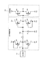
図6は従来の技術における出力保護回路の等価回路である(例えば特許文献1参照)。図6において、21は出力端子(ボンディングパッド)、Q1,Q2,Q3,Q4はダイオード形態にしてクランプFETを構成するNチャネル型のトランジスタ、Rは抵抗素子、Dはダイオード、H1,H2はアルミ配線、Q5は内部回路22におけるPチャネル型の出力トランジスタ、Q6はNチャネル型の出力トランジスタである。
FIG. 6 is an equivalent circuit of a conventional output protection circuit (see, for example, Patent Document 1). In FIG. 6, 21 is an output terminal (bonding pad), Q1, Q2, Q3, Q4 are N-channel transistors constituting a clamp FET in the form of a diode, R is a resistance element, D is a diode, and H1, H2 are aluminum. Wiring Q5 is a P-channel output transistor in the
トランジスタQ1は、そのソースが出力端子21と抵抗素子Rとの間のアルミ配線H1に接続され、ドレインが電源電位Vcc(例えば5V)に接続され、ゲート電極がドレインに短絡されている。トランジスタQ2は、そのドレインがアルミ配線H1に接続され、ソースが接地電位Vss(例えば0V)に接続され、ゲート電極がドレインに短絡されている。トランジスタQ1,Q2の閾値電圧は10V〜20Vである。
The source of the transistor Q1 is connected to the aluminum wiring H1 between the
トランジスタQ3は、そのソースが抵抗素子Rから内部回路22に延びるアルミ配線H2に接続され、ドレインが電源電位Vccに接続され、ゲート電極がソースに短絡されている。トランジスタQ4は、そのドレインがアルミ配線H2に接続され、ソースが接地電位Vssに接続され、ゲート電極がソースに短絡されている。トランジスタQ3の閾値電圧は3V〜5Vである。
Transistor Q3 has a source connected to aluminum wiring H2 extending from resistance element R to
プラス(+)の過大な電荷が出力端子21から流入すると、それをゲート電極に入力するトランジスタQ2が導通状態となり、その過大な電荷の一部を接地電位Vssへ放出する。過大な電荷のその他の部分は、抵抗素子Rによって減衰された後、トランジスタQ3のゲート電極に達する。すると、トランジスタQ3が導通状態となる。このとき、トランジスタQ3の閾値電圧が3V〜5V程度と低いため、P型出力トランジスタQ5、N型出力トランジスタQ6が破壊に至る前に、過大な電荷をトランジスタQ3を介して迅速に電源電位Vccに放出することができる。なお、ダイオードDもブレイクダウンして過大な電荷の一部を接地電位Vssに放出する。
When an excessive plus (+) charge flows from the
また、マイナス(−)の過大な電荷が出力端子21から流入すると、トランジスタQ2がブレイクダウンを起して、上記過大な電荷の一部を放出する。一方、マイナスの過大な電荷によってトランジスタQ1が導通状態となり、その電荷の一部を電源電位Vccに放出する。マイナスの過大な電荷は、抵抗素子Rによってさらに減衰された後に、トランジスタQ4が導通して接地電位Vssに放出される。
Further, when a minus (−) excessive charge flows in from the
このようにして、内部回路22を構成している出力トランジスタQ5,Q6が過大な電荷によって破壊されることを防止できる。
ところで、製造工程での工程数の増大を防ぎ低コスト化を図るために、出力保護回路を構成するトランジスタは、内部回路を構成するトランジスタと同時に形成される。内部回路のトランジスタは高耐圧系のトランジスタと低耐圧系のトランジスタとの2種類を有するものが多い。これは、半導体装置のロジック回路部はデバイス動作特性(高速性、回路面積の縮小など)の観点から、外部から供給される電圧が3V〜5Vであるのに対して、デバイスの使用用途から、出力回路は5V〜60Vの高電圧が入力されるためである。 By the way, in order to prevent an increase in the number of steps in the manufacturing process and to reduce the cost, the transistors constituting the output protection circuit are formed simultaneously with the transistors constituting the internal circuit. Many of the transistors in the internal circuit have two types, a high withstand voltage transistor and a low withstand voltage transistor. This is because the logic circuit part of the semiconductor device has a voltage of 3 V to 5 V supplied from the outside in terms of device operation characteristics (high speed performance, reduction in circuit area, etc.), whereas from the usage application of the device, This is because a high voltage of 5V to 60V is input to the output circuit.
これに対し、出力保護回路は、高耐圧系のトランジスタや寄生MOSトランジスタで構成される。これは出力保護回路の耐圧を稼ぐためである。上記の特許文献1の出力保護回路では、寄生MISFETとMISFETを組み合わせて使用し出力保護回路の耐圧を稼いでいる。 On the other hand, the output protection circuit is composed of a high breakdown voltage transistor or a parasitic MOS transistor. This is to increase the withstand voltage of the output protection circuit. In the output protection circuit of the above-mentioned patent document 1, a parasitic MISFET and a MISFET are used in combination to increase the withstand voltage of the output protection circuit.
しかし、上記従来の出力保護回路は複数のトランジスタを用いて構成されているため、出力保護回路の領域が大きくなり、半導体装置の縮小化がむずかしいものとなっている。 However, since the conventional output protection circuit is configured using a plurality of transistors, the area of the output protection circuit becomes large, and it is difficult to reduce the size of the semiconductor device.
本発明は、このような事情に鑑みて創作したものであり、過電圧に伴う大きな電流を効果的に逃がせる出力保護回路を、回路サイズを縮小した状態で提供することを目的としている。 The present invention has been created in view of such circumstances, and an object thereof is to provide an output protection circuit capable of effectively escaping a large current caused by an overvoltage in a state where the circuit size is reduced.
本発明による出力保護回路は、半導体装置において出力端子と内部回路との間に介挿されるものであって、半導体基板主面上に選択的に形成されたフィールド酸化膜に内外を区画するガードバンド領域が形成され、前記ガードバンド領域に囲まれた主面部分に、高耐圧トランジスタとともに出力保護トランジスタが形成され、前記出力保護トランジスタと前記高耐圧トランジスタとはドレインを共通にする状態に構成されているものである。 An output protection circuit according to the present invention is interposed between an output terminal and an internal circuit in a semiconductor device, and is a guard band that divides the inside and the outside into a field oxide film selectively formed on a main surface of a semiconductor substrate. A region is formed, and an output protection transistor is formed together with a high breakdown voltage transistor on a main surface portion surrounded by the guard band region, and the output protection transistor and the high breakdown voltage transistor are configured to have a common drain. It is what.
この構成によれば、共通のガードバンド領域の内部に高耐圧トランジスタと出力保護トランジスタとを配置し、さらに、高耐圧トランジスタのドレインと出力保護トランジスタのドレインとを共通化してあるので、高耐圧トランジスタと出力保護トランジスタの組み合わせからなる出力保護回路の占有面積を削減することが可能となる。 According to this configuration, the high breakdown voltage transistor and the output protection transistor are arranged inside the common guard band region, and the drain of the high breakdown voltage transistor and the drain of the output protection transistor are shared. It is possible to reduce the area occupied by the output protection circuit comprising the combination of the output protection transistor and the output protection transistor.
上記構成の出力保護回路において、前記出力保護トランジスタのゲート電極は、その一部が前記高耐圧トランジスタのドレインのフィールド酸化膜の上面に重なり合う状態に構成されているという態様がある。このように構成すれば、出力保護トランジスタのゲート電極を高耐圧トランジスタのドレインフィールド酸化膜に重ね合わせていることから、出力保護回路の占有面積をさらに削減することが可能となる。 In the output protection circuit configured as described above, there is a mode in which a part of the gate electrode of the output protection transistor is configured to overlap the upper surface of the field oxide film of the drain of the high breakdown voltage transistor. With this configuration, the area of the output protection circuit can be further reduced because the gate electrode of the output protection transistor is overlaid on the drain field oxide film of the high breakdown voltage transistor.
また上記構成の出力保護回路において、前記出力保護トランジスタのゲート電極が重なり合う前記フィールド酸化膜の下部にN型低濃度領域が形成されているという態様がある。このように構成すれば、高耐圧トランジスタのドレイン領域から印加される高電圧のサージに対する電界が緩和され、より大きなサージ耐量が確保される。 In the output protection circuit having the above-described configuration, an N-type low concentration region is formed below the field oxide film where the gate electrodes of the output protection transistors overlap. If comprised in this way, the electric field with respect to the high voltage surge applied from the drain region of a high voltage | pressure-resistant transistor will be relieve | moderated, and a larger surge tolerance is ensured.
また上記構成の出力保護回路において、前記出力保護トランジスタのゲート酸化膜は、前記高耐圧トランジスタのゲート酸化膜より薄く形成されているという態様がある。このように構成すれば、出力保護トランジスタの電流能力が増大し、内部回路に対する対サージ保護機能を向上させることが可能となる。 In the output protection circuit having the above configuration, the gate oxide film of the output protection transistor is formed thinner than the gate oxide film of the high breakdown voltage transistor. If comprised in this way, the current capability of an output protection transistor will increase, and it will become possible to improve the surge protection function with respect to an internal circuit.
また上記構成の出力保護回路において、前記出力保護トランジスタのソースは、前記ガードバンド領域に接する状態に構成されているという態様がある。このように構成すれば、出力保護回路の占有面積をさらに削減することが可能となる。 In the output protection circuit having the above-described configuration, the source of the output protection transistor is configured to be in contact with the guard band region. With this configuration, it is possible to further reduce the area occupied by the output protection circuit.
また上記構成の出力保護回路において、前記出力保護トランジスタは、その形成方向が前記高耐圧トランジスタの形成方向に対して同一方向とされているという態様がある。 In the output protection circuit having the above configuration, the output protection transistor may be formed in the same direction as the high breakdown voltage transistor.
また上記構成の出力保護回路において、前記出力保護トランジスタは、その形成方向が前記高耐圧トランジスタの形成方向に対して直角方向とされているという態様もある。 In the output protection circuit having the above configuration, the output protection transistor may be formed in a direction perpendicular to the formation direction of the high breakdown voltage transistor.
後者の直角方向に配置した場合には、高耐圧トランジスタと出力保護トランジスタからなるトランジスタ対を繰り返し配置するときに、前者の同一方向に配置する場合に比べて、その繰り返しピッチが小さくなり、さらなる高密度配置が可能となる。 When the latter is arranged in a perpendicular direction, when the transistor pair composed of the high voltage transistor and the output protection transistor is repeatedly arranged, the repetition pitch is smaller than that of the former case in which the transistor pair is arranged in the same direction. Density arrangement is possible.
本発明によれば、共通のガードバンド領域の内部に高耐圧トランジスタと出力保護トランジスタとの両者を組み込み、さらに、両トランジスタのドレインを共通化してあるので、出力保護回路の占有面積を削減することができ、ひいてはコスト力のある出力保護回路を提供できる。 According to the present invention, both the high breakdown voltage transistor and the output protection transistor are incorporated in the common guard band region, and the drains of both transistors are shared, so that the area occupied by the output protection circuit is reduced. As a result, a cost-effective output protection circuit can be provided.
以下、本発明にかかわる出力保護回路の実施の形態を図面を用いて詳細に説明する。 Embodiments of an output protection circuit according to the present invention will be described below in detail with reference to the drawings.
(実施の形態1)
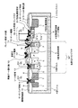
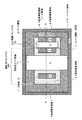
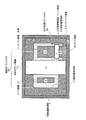
図1は本発明の実施の形態1における出力保護回路の構造断面図、図2はその平面図、図3は出力保護回路の等価回路図、図4は適用状態説明図である。図1は図2でのA−A′線に沿った断面図である。
(Embodiment 1)
FIG. 1 is a structural sectional view of an output protection circuit according to Embodiment 1 of the present invention, FIG. 2 is a plan view thereof, FIG. 3 is an equivalent circuit diagram of the output protection circuit, and FIG. FIG. 1 is a cross-sectional view taken along the line AA 'in FIG.
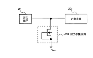
まず、全体的な概要を図4を用いて説明する。図4において、21は出力端子、22は内部回路、23は出力端子21と内部回路22との間に介挿されて、出力端子21に印加される過電圧から内部回路22を保護する出力保護回路である。
First, an overall outline will be described with reference to FIG. In FIG. 4,
次に、本実施の形態における出力保護回路23のレイアウトを図1および図2を用いて説明する。 Next, the layout of the output protection circuit 23 in this embodiment will be described with reference to FIGS.
図1、図2において、1は半導体基板としてのシリコンウエハ、2はP型ウェル、3はN型ウェル、4はガードバンド領域、5はN型低濃度領域、6はN型高濃度領域(ソース)、7はP型低濃度領域、8はP型高濃度領域、9はフィールド酸化膜、10は厚膜ゲート酸化膜、11は薄膜ゲート酸化膜、12は高耐圧ゲート電極、13はソース領域、14はドレイン領域、15は出力保護トランジスタのゲート電極、16は層間絶縁膜、QHは高耐圧トランジスタ、QLは出力保護トランジスタである。 1 and 2, 1 is a silicon wafer as a semiconductor substrate, 2 is a P-type well, 3 is an N-type well, 4 is a guard band region, 5 is an N-type low concentration region, and 6 is an N-type high concentration region ( (Source), 7 is a P-type low concentration region, 8 is a P-type high concentration region, 9 is a field oxide film, 10 is a thick gate oxide film, 11 is a thin gate oxide film, 12 is a high breakdown voltage gate electrode, and 13 is a source. 14 is a drain region, 15 is a gate electrode of an output protection transistor, 16 is an interlayer insulating film, QH is a high breakdown voltage transistor, and QL is an output protection transistor.
まず、高耐圧トランジスタQHの構成について説明する。 First, the configuration of the high breakdown voltage transistor QH will be described.
シリコンウエハ1にP型ウェル2が形成され、その表面に選択酸化によって形成されたフィールド酸化膜9が高耐圧トランジスタQHの領域と出力保護トランジスタQLの領域を規定している。フィールド酸化膜9において、内外を区画するガードバンド領域4が形成され、ガードバンド領域4に囲まれた主面部分に、高耐圧トランジスタQHとともに出力保護トランジスタQLが形成されている。
A P-
高耐圧トランジスタQHでは、高耐圧ゲート電極12、ソース領域13およびドレイン領域14がフィールド酸化膜9によって分離されている。高耐圧ゲート電極12とソース領域13を分離しているフィールド酸化膜9の下部および高耐圧ゲート電極12とドレイン領域14を分離しているフィールド酸化膜9の下部にそれぞれN型低濃度領域5が形成されている。ソース領域13とガードバンド領域4とを分離しているフィールド酸化膜9の下部には、N型低濃度領域5とチャンネルストップ領域としてのP型低濃度領域7とが形成されている。また、ガードバンド領域4の外側に位置するフィールド酸化膜9の下部にもP型低濃度領域7が形成されている。ソース領域13とドレイン領域14の下部にはN型ウェル3が形成されている。P型ウェル2と高耐圧ゲート電極12との間のゲート酸化膜は、高耐圧構造とするために厚膜ゲート酸化膜10として形成されている。
In the high breakdown voltage transistor QH, the high breakdown
次に、出力保護トランジスタQLの構成について説明する。 Next, the configuration of the output protection transistor QL will be described.
出力保護トランジスタQLのソース・ゲート・ドレインの形成方向は高耐圧トランジスタQHのソース・ゲート・ドレインの形成方向に対して同一方向となっている。出力保護トランジスタQLでは、共通ドレイン領域14を共通のドレイン領域とするMOSトランジスタで構成されている。出力保護トランジスタのゲート電極15は、共通ドレイン領域14に接しているフィールド酸化膜9の上に乗り上がって重なり合う状態で形成されている。そして、そのフィールド酸化膜9の下部にN型低濃度領域5が形成されている。この構成により、出力端子21から共通ドレイン領域14に印加される高電圧のサージに対する電界を緩和し、より大きなサージ耐量を確保している。
The source / gate / drain formation direction of the output protection transistor QL is the same as the source / gate / drain formation direction of the high breakdown voltage transistor QH. The output protection transistor QL includes a MOS transistor having the
また、出力保護トランジスタQLにおいて、ゲート電極15の下方のゲート酸化膜は、高耐圧トランジスタQHの厚膜ゲート酸化膜10よりも薄い状態の薄膜ゲート酸化膜11に形成されている。すなわち、この薄膜ゲート酸化膜11は、内部回路22におけるロジック回路を構成する低耐圧トランジスタと同じ膜厚とされている。このように構成することにより、出力保護トランジスタQLの電流能力を向上させている。
In the output protection transistor QL, the gate oxide film below the gate electrode 15 is formed as a thin gate oxide film 11 that is thinner than the thick
N型高濃度領域6は出力保護トランジスタQLのソース領域を構成し、このソース領域を構成するN型高濃度領域6はP型高濃度領域8に接し、P型高濃度領域8はガードバンド領域4に接している。この構成も、出力保護回路の占有面積を削減する上で有効である。
The N-type
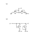
図3(a),(b)は図1、図2に示す出力保護回路の等価回路である。図3(a)は配置関係を図1に合わせて図示したものである。図3(b)は図3(a)を図6に擬して展開したものである。 FIGS. 3A and 3B are equivalent circuits of the output protection circuit shown in FIGS. FIG. 3A illustrates the arrangement relationship with FIG. FIG. 3B is a development of FIG. 3A imitating FIG.
プラス(+)の過大な電荷が出力端子21から流入すると、それをゲート電極に入力するトランジスタQ2(高耐圧トランジスタQH)が導通状態となり、その過大な電荷の一部を接地電位Vssへ放出する。
When an excessive plus (+) charge flows from the
また、マイナス(−)の過大な電荷が出力端子21から流入すると、トランジスタQ2がブレイクダウンを起して、上記過大な電荷の一部を放出する。それをゲート電極に入力するトランジスタQ4(出力保護トランジスタQL)が導通状態となり、その過大な電荷の一部を接地電位Vssへ放出する。
Further, when a minus (−) excessive charge flows in from the
上記は出力端子21と接地電位Vssとの間に介挿される高耐圧トランジスタQHと出力保護トランジスタQLとの組み合わせであったが、出力端子21と電源電位Vccとの間に介挿される高耐圧トランジスタQHと出力保護トランジスタQLとの組み合わせについても同様に構成してもよい。
The above is a combination of the high breakdown voltage transistor QH and the output protection transistor QL interposed between the
(実施の形態2)
図5は本発明の実施の形態2における出力保護回路の平面図である。図5において、実施の形態1の図2におけるのと同じ符号は同一構成要素を指している。実施の形態1では、出力保護トランジスタQLの形成方向が高耐圧トランジスタQHの形成方向と同一方向になっているのに対して、本実施の形態では、高耐圧トランジスタQHのソース・ゲート・ドレインの形成方向に対して出力保護トランジスタQLのソース・ゲート・ドレインの形成方向が直角方向とされている。その他の構成については、実施の形態1と同様であるので、説明を省略する。
(Embodiment 2)
FIG. 5 is a plan view of the output protection circuit according to the second embodiment of the present invention. In FIG. 5, the same reference numerals as those in FIG. 2 of the first embodiment indicate the same components. In the first embodiment, the output protection transistor QL is formed in the same direction as the high breakdown voltage transistor QH. In the present embodiment, the source, gate, and drain of the high breakdown voltage transistor QH The formation direction of the source / gate / drain of the output protection transistor QL is perpendicular to the formation direction. Since other configurations are the same as those in the first embodiment, description thereof is omitted.
本実施の形態によれば、トランジスタを横方向に繰り返し配置する場合に、出力保護トランジスタQLを共通ドレイン領域14の横側方に配置した場合よりも繰り返しピッチが小さくなり、さらなる高密度配置が可能となる。
According to the present embodiment, when the transistors are repeatedly arranged in the lateral direction, the repetition pitch is smaller than when the output protection transistor QL is disposed laterally of the
本発明の出力保護回路は、半導体回路の出力回路に印加される異常電圧を効果的に外部に排出し、出力回路を保護する上で有用である。 The output protection circuit of the present invention is useful for protecting the output circuit by effectively discharging the abnormal voltage applied to the output circuit of the semiconductor circuit to the outside.
1 シリコンウエハ
2 P型ウェル
3 N型ウェル
4 ガードバンド領域
5 N型低濃度領域
6 N型高濃度領域(ソース領域)
7 P型低濃度領域
8 P型高濃度領域
9 フィールド酸化膜
10 厚膜ゲート酸化膜
11 薄膜ゲート酸化膜
12 高耐圧ゲート電極
13 ソース領域
14 共通ドレイン領域
15 出力保護トランジスタのゲート電極
16 層間絶縁膜
21 出力端子
22 内部回路
23 出力保護回路
QH 高耐圧トランジスタ
QL 出力保護トランジスタ
1 Silicon wafer 2 P-type well 3 N-type well 4 Guard band region 5 N-type low concentration region 6 N-type high concentration region (source region)
7 P-type low concentration region 8 P-type
Claims (7)
半導体基板主面上に選択的に形成されたフィールド酸化膜に内外を区画するガードバンド領域が形成され、
前記ガードバンド領域に囲まれた主面部分に、高耐圧トランジスタとともに出力保護トランジスタが形成され、
前記出力保護トランジスタと前記高耐圧トランジスタとはドレインを共通にする状態に構成されている出力保護回路。 An output protection circuit inserted between an output terminal and an internal circuit in a semiconductor device,
A guard band region that partitions the inside and outside of the field oxide film selectively formed on the main surface of the semiconductor substrate is formed,
In the main surface portion surrounded by the guard band region, an output protection transistor is formed together with a high breakdown voltage transistor,
The output protection circuit configured such that the output protection transistor and the high breakdown voltage transistor share a drain.
Priority Applications (1)
| Application Number | Priority Date | Filing Date | Title |
|---|---|---|---|
| JP2006271572A JP2008091663A (en) | 2006-10-03 | 2006-10-03 | Output protection circuit |
Applications Claiming Priority (1)
| Application Number | Priority Date | Filing Date | Title |
|---|---|---|---|
| JP2006271572A JP2008091663A (en) | 2006-10-03 | 2006-10-03 | Output protection circuit |
Publications (1)
| Publication Number | Publication Date |
|---|---|
| JP2008091663A true JP2008091663A (en) | 2008-04-17 |
Family
ID=39375504
Family Applications (1)
| Application Number | Title | Priority Date | Filing Date |
|---|---|---|---|
| JP2006271572A Pending JP2008091663A (en) | 2006-10-03 | 2006-10-03 | Output protection circuit |
Country Status (1)
| Country | Link |
|---|---|
| JP (1) | JP2008091663A (en) |
Cited By (1)
| Publication number | Priority date | Publication date | Assignee | Title |
|---|---|---|---|---|
| JP2017517884A (en) * | 2014-05-04 | 2017-06-29 | 無錫華潤上華半導体有限公司 | Semiconductor device with ESD protection structure |
-
2006
- 2006-10-03 JP JP2006271572A patent/JP2008091663A/en active Pending
Cited By (1)
| Publication number | Priority date | Publication date | Assignee | Title |
|---|---|---|---|---|
| JP2017517884A (en) * | 2014-05-04 | 2017-06-29 | 無錫華潤上華半導体有限公司 | Semiconductor device with ESD protection structure |
Similar Documents
| Publication | Publication Date | Title |
|---|---|---|
| TWI553819B (en) | Semiconductor integrated circuit | |
| US9576947B2 (en) | Semiconductor integrated circuit device | |
| US20050045955A1 (en) | Integrated circuit device having input/output electrostatic discharge protection cell equipment with electrostatic discharge protection element and power clamp | |
| JPH0837284A (en) | Semiconductor integrated circuit device | |
| US20080173899A1 (en) | Semiconductor device | |
| JP2010016177A (en) | Electrostatic discharge protection element | |
| JP2006060191A (en) | THIN FILM SEMICONDUCTOR DEVICE AND ITS MANUFACTURING METHOD, ELECTRO-OPTICAL DEVICE, ELECTRONIC DEVICE | |
| KR20050043640A (en) | Electrostatic breakdown protection device | |
| KR100297151B1 (en) | Semiconductor integrated circuit | |
| JP2001217414A (en) | Semiconductor device | |
| JP5241109B2 (en) | Semiconductor integrated circuit device | |
| JP2008078361A (en) | Semiconductor integrated circuit device | |
| JP2008091663A (en) | Output protection circuit | |
| JPH07335894A (en) | Semiconductor device | |
| JP2970826B2 (en) | Protection circuit built-in IC and display device driving IC | |
| JP2004247455A (en) | Semiconductor device | |
| JP2008235625A (en) | Semiconductor integrated circuit | |
| US12107415B2 (en) | Electrostatic discharge protection circuit and electronic circuit | |
| JP2007227697A (en) | Semiconductor device and semiconductor integrated device | |
| KR20070029059A (en) | Semiconductor devices | |
| KR20250063759A (en) | Semiconductor device | |
| JP2009016725A (en) | Semiconductor device | |
| JP2006186399A (en) | Electrostatic destruction protective circuit | |
| JP2005322943A (en) | Input protection circuit | |
| JP2004172634A (en) | Electrostatic destruction prevention protective circuit of semiconductor device |