JP2008071663A - Organic EL elements, electronic devices - Google Patents
Organic EL elements, electronic devices Download PDFInfo
- Publication number
- JP2008071663A JP2008071663A JP2006250402A JP2006250402A JP2008071663A JP 2008071663 A JP2008071663 A JP 2008071663A JP 2006250402 A JP2006250402 A JP 2006250402A JP 2006250402 A JP2006250402 A JP 2006250402A JP 2008071663 A JP2008071663 A JP 2008071663A
- Authority
- JP
- Japan
- Prior art keywords
- organic
- substrate
- adhesive
- sealing glass
- sealing
- Prior art date
- Legal status (The legal status is an assumption and is not a legal conclusion. Google has not performed a legal analysis and makes no representation as to the accuracy of the status listed.)
- Withdrawn
Links
- 239000000758 substrate Substances 0.000 claims abstract description 61
- 239000000853 adhesive Substances 0.000 claims abstract description 37
- 230000001070 adhesive effect Effects 0.000 claims abstract description 36
- 230000003746 surface roughness Effects 0.000 claims abstract description 15
- 238000007789 sealing Methods 0.000 claims description 18
- 239000005394 sealing glass Substances 0.000 abstract description 34
- QVGXLLKOCUKJST-UHFFFAOYSA-N atomic oxygen Chemical compound [O] QVGXLLKOCUKJST-UHFFFAOYSA-N 0.000 abstract description 5
- 238000005422 blasting Methods 0.000 abstract description 5
- 239000001301 oxygen Substances 0.000 abstract description 5
- 229910052760 oxygen Inorganic materials 0.000 abstract description 5
- 239000007788 liquid Substances 0.000 description 12
- 238000000034 method Methods 0.000 description 9
- 230000006866 deterioration Effects 0.000 description 5
- 239000000203 mixture Substances 0.000 description 5
- 230000002940 repellent Effects 0.000 description 5
- 239000005871 repellent Substances 0.000 description 5
- 230000000694 effects Effects 0.000 description 4
- 239000000463 material Substances 0.000 description 4
- 239000011295 pitch Substances 0.000 description 4
- VYPSYNLAJGMNEJ-UHFFFAOYSA-N Silicium dioxide Chemical compound O=[Si]=O VYPSYNLAJGMNEJ-UHFFFAOYSA-N 0.000 description 3
- 239000002274 desiccant Substances 0.000 description 3
- 239000011521 glass Substances 0.000 description 3
- 238000004519 manufacturing process Methods 0.000 description 3
- 239000002184 metal Substances 0.000 description 3
- 229910052751 metal Inorganic materials 0.000 description 3
- 230000003287 optical effect Effects 0.000 description 3
- 229910004298 SiO 2 Inorganic materials 0.000 description 2
- 238000005401 electroluminescence Methods 0.000 description 2
- 230000009477 glass transition Effects 0.000 description 2
- 230000005525 hole transport Effects 0.000 description 2
- 238000000059 patterning Methods 0.000 description 2
- 239000011347 resin Substances 0.000 description 2
- 229920005989 resin Polymers 0.000 description 2
- 229910052814 silicon oxide Inorganic materials 0.000 description 2
- 239000002904 solvent Substances 0.000 description 2
- 238000007740 vapor deposition Methods 0.000 description 2
- 239000004925 Acrylic resin Substances 0.000 description 1
- 229920000178 Acrylic resin Polymers 0.000 description 1
- YCKRFDGAMUMZLT-UHFFFAOYSA-N Fluorine atom Chemical compound [F] YCKRFDGAMUMZLT-UHFFFAOYSA-N 0.000 description 1
- CTQNGGLPUBDAKN-UHFFFAOYSA-N O-Xylene Chemical compound CC1=CC=CC=C1C CTQNGGLPUBDAKN-UHFFFAOYSA-N 0.000 description 1
- 239000006061 abrasive grain Substances 0.000 description 1
- 230000002411 adverse Effects 0.000 description 1
- 229910052782 aluminium Inorganic materials 0.000 description 1
- XAGFODPZIPBFFR-UHFFFAOYSA-N aluminium Chemical compound [Al] XAGFODPZIPBFFR-UHFFFAOYSA-N 0.000 description 1
- 239000012298 atmosphere Substances 0.000 description 1
- 238000009412 basement excavation Methods 0.000 description 1
- 239000012159 carrier gas Substances 0.000 description 1
- 238000010586 diagram Methods 0.000 description 1
- 238000009792 diffusion process Methods 0.000 description 1
- 239000003822 epoxy resin Substances 0.000 description 1
- 238000005530 etching Methods 0.000 description 1
- 229910052731 fluorine Inorganic materials 0.000 description 1
- 239000011737 fluorine Substances 0.000 description 1
- 239000011261 inert gas Substances 0.000 description 1
- 239000011159 matrix material Substances 0.000 description 1
- 239000011368 organic material Substances 0.000 description 1
- 230000035699 permeability Effects 0.000 description 1
- 238000000206 photolithography Methods 0.000 description 1
- 238000009832 plasma treatment Methods 0.000 description 1
- 229920000647 polyepoxide Polymers 0.000 description 1
- 229920001721 polyimide Polymers 0.000 description 1
- 239000009719 polyimide resin Substances 0.000 description 1
- 238000003672 processing method Methods 0.000 description 1
- 239000010453 quartz Substances 0.000 description 1
- 239000007787 solid Substances 0.000 description 1
- 238000004544 sputter deposition Methods 0.000 description 1
- 229920003002 synthetic resin Polymers 0.000 description 1
- 239000000057 synthetic resin Substances 0.000 description 1
- XLYOFNOQVPJJNP-UHFFFAOYSA-N water Substances O XLYOFNOQVPJJNP-UHFFFAOYSA-N 0.000 description 1
- 239000008096 xylene Substances 0.000 description 1
Images
Landscapes
- Electroluminescent Light Sources (AREA)
Abstract
【課題】外部からの酸素や水分の侵入を低減する有機EL素子、電子機器を提供する。
【解決手段】
ショットブラストによって、封止ガラス32の接着面36に、面粗度Ra=0.1〜10
μmとなる微小の凹凸面を設けた。一方、接着面36に対向する基板Sの第1領域34は
平坦である。そして、基板Sの第1領域34と封止ガラス32の接着面36とを接着剤3
8を介して貼り合わせた。
【選択図】図2An organic EL element and an electronic device that reduce intrusion of oxygen and moisture from the outside are provided.
[Solution]
By shot blasting, the surface roughness Ra = 0.1 to 10 is applied to the adhesive surface 36 of the sealing glass 32.
A minute uneven surface of μm was provided. On the other hand, the first region 34 of the substrate S facing the bonding surface 36 is flat. Then, the first region 34 of the substrate S and the adhesive surface 36 of the sealing glass 32 are bonded to the adhesive 3.
8 was bonded together.
[Selection] Figure 2
Description
本発明は、有機EL素子、電子機器に関する。 The present invention relates to an organic EL element and an electronic device.
従来、有機エレクトロルミネッセンス素子(以下、「有機EL素子」という)は、ガラ
ス基板上に、陽極、正孔輸送層、発光層、陰極を積層形成した構成を有している。ここで
、正孔輸送層や発光層に利用する固体有機材料は、水分や酸素などに侵されやすく、大気
中で有機EL素子を駆動するとその発光特性が急激に劣化する。そこで、発光層及び一方
の電極を囲う封止ガラス板により密封室を設けた有機EL素子がある(例えば、特許文献
1)。
Conventionally, an organic electroluminescence element (hereinafter referred to as “organic EL element”) has a configuration in which an anode, a hole transport layer, a light emitting layer, and a cathode are laminated on a glass substrate. Here, the solid organic material used for the hole transport layer and the light emitting layer is easily attacked by moisture, oxygen, and the like, and when the organic EL element is driven in the air, the light emission characteristics thereof are rapidly deteriorated. Therefore, there is an organic EL element in which a sealing chamber is provided by a sealing glass plate surrounding a light emitting layer and one electrode (for example, Patent Document 1).
この特許文献1の有機EL素子は、前記密封室内に不活性ガスを封入するとともに、封
止ガラス板の内面に吸湿性多孔質層を設けている。この結果、封止ガラス板により大気か
らの水分の内部への拡散が有効に防止され、素子特性への悪影響を排除することができる
。さらに、多孔質層によって、製造時において素子部の表面や透明電極の表面に吸着され
ている水分が除去され、密封室内を水分のない状態に維持し、素子の長寿命化を図ってい
た。
しかしながら、特許文献1の有機EL素子では、ガラス基板と封止ガラス板との隙間か
ら水分や酸素が流入する。また、多孔質層を形成する新たな製造工程が必要であった。
本発明は、上記課題を解決するためになされたものであり、その目的は、外部からの酸
素や水分の侵入を低減する有機EL素子、電子機器を提供することにある。
However, in the organic EL element of Patent Document 1, moisture and oxygen flow from the gap between the glass substrate and the sealing glass plate. In addition, a new manufacturing process for forming the porous layer is required.
The present invention has been made to solve the above-described problems, and an object of the present invention is to provide an organic EL element and an electronic apparatus that reduce intrusion of oxygen and moisture from the outside.
上記問題点を解決するために、本発明は、複数の表示素子を備えた素子基板と前記素子
基板と接着剤を介して接着されて前記複数の表示素子を封止する封止基板とを備えた有機
EL素子において、前記封止基板の接着面に面粗度Ra=0.1〜10μmの凹凸を形成
した。
In order to solve the above problems, the present invention includes an element substrate including a plurality of display elements, and a sealing substrate that is bonded to the element substrate via an adhesive to seal the plurality of display elements. In the organic EL element, irregularities having a surface roughness Ra = 0.1 to 10 μm were formed on the bonding surface of the sealing substrate.
この発明によれば、接着面に形成した面粗度Ra=0.1〜10μmの凹凸を封止基板
側に形成したので、素子基板上に形成される外部に引き回される配線を形成する際に、そ
の接着剤を介して封止基板の接着面と対向する配線の形状を特別な形状にすることなく形
成することができる。
According to the present invention, since the unevenness with the surface roughness Ra = 0.1 to 10 μm formed on the bonding surface is formed on the sealing substrate side, the wiring routed to the outside formed on the element substrate is formed. In this case, the shape of the wiring facing the bonding surface of the sealing substrate via the adhesive can be formed without any special shape.
本発明は、前記素子基板の接着面は平坦である。この結果、素子基板上に外部へ引き回
される配線を形成する際に、配線に与える影響が少なく、配線の劣化を低減することがで
きる。
In the present invention, the bonding surface of the element substrate is flat. As a result, when the wiring routed to the outside is formed on the element substrate, there is little influence on the wiring, and deterioration of the wiring can be reduced.
本発明は、複数の表示素子を備えた素子基板と前記素子基板と接着剤を介して接着され
て前記複数の表示素子を封止する封止基板とを備えた有機EL素子において、前記素子基
板の接着面に面粗度Ra=0.1〜10μmの凹凸を形成した。
The present invention relates to an organic EL element comprising an element substrate having a plurality of display elements and a sealing substrate that is bonded to the element substrate via an adhesive and seals the plurality of display elements. Irregularities having a surface roughness Ra = 0.1 to 10 μm were formed on the adhesion surface.
この発明によれば、凹凸を素子基板側に形成したが、その凹凸は面粗度Ra=0.1〜
10μmの非常に細かい凹凸面なので、素子基板上に外部へ引き回される配線を形成する
際に、配線に与える影響が少なく、配線の劣化を低減することができる。
According to the present invention, the unevenness is formed on the element substrate side, and the unevenness has a surface roughness Ra = 0.1 to 0.1.
Since it is a very fine uneven surface of 10 μm, there is little influence on the wiring when forming the wiring routed to the outside on the element substrate, and the deterioration of the wiring can be reduced.
本発明は、前記封止基板の接着面は平坦である。この結果、封止基板の接着面の形状を
特別な形状にすることなく形成することができる。
本発明は、前記接着面における凹凸は前記表示素子を囲むように環状に形成されている
。この結果、この発明によれば、前記表示素子を囲む周方向のいずれの方向においても良
好な封止効果を得ることができる。
In the present invention, the adhesion surface of the sealing substrate is flat. As a result, the bonding surface of the sealing substrate can be formed without a special shape.
In the present invention, the unevenness on the bonding surface is formed in an annular shape so as to surround the display element. As a result, according to the present invention, a good sealing effect can be obtained in any of the circumferential directions surrounding the display element.
本発明は、上記に記載の有機EL素子を備えた。この発明によれば、前記複数の表示素
子を良好に封止し、また、配線の劣化を防止できるので、高性能の電子機器を提供するこ
とができる。
The present invention includes the organic EL element described above. According to the present invention, since the plurality of display elements can be well sealed and the deterioration of the wiring can be prevented, a high-performance electronic device can be provided.
以下、本発明を具体化した実施形態を図面と共に説明する。
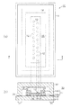
図1(a)は、感光体に光を照射する光書き込みヘッドのような電子写真プリンタに適
用される発光素子アレイ10の上面図であり、図1(b)は、図1(a)中a−a線断面
図である。
DESCRIPTION OF THE PREFERRED EMBODIMENTS Embodiments embodying the present invention will be described below with reference to the drawings.
FIG. 1A is a top view of a light-emitting
図1(a)に示すように、発光素子アレイ10は、素子基板としての基板S上に表示素
子としての有機エレクトロルミネッセンス素子(以下、「有機EL素子」という)12を
複数個配列している。本実施形態の発光素子アレイ10は、縦一列に等ピッチに配列され
た複数個(本実施形態では、10個)の有機EL素子12が2列配列されている。そして
、各有機EL素子12は、隣接する他の列の有機EL素子12と縦方向に半ピッチだけず
れるようにして配置されている。つまり、各有機EL素子12は、千鳥格子状に配列され
ている。
As shown in FIG. 1A, the light
また、複数の有機EL素子12の周囲には、その複数の有機EL素子12全体を囲むよ
うにバンク14が形成されている。本実施形態におけるバンク14は、図1(a)に示す
ように、複数の有機EL素子12全体を囲むように略四角形状を成している。
A
図1(b)に示すように、バンク14は、基板S上に形成された親液性バンク14aと
、該親液性バンク14a上に形成された撥液性バンク14bとから構成されている。親液
性バンク14aの一部は、撥液性バンク14bより基板S中央側に張り出すようにして形
成されている。親液性バンク14aは、元来、親液性を備えた材料であって、例えば、酸
化珪素(SiO2)で構成されたものである。また、親液性を備えていないものであって
も、通常用いられる公知の親液化処理を施すことで表面を親液化したものであってもよい
。一方、撥液性バンク14bは、元来、撥液性を備えた材料、例えば、フッ素系樹脂で構
成されたものであってもよい。また、撥液性を備えていないものであっても、通常用いら
れるアクリル樹脂やポリイミド樹脂等の有機樹脂をパターン形成し、CF4 プラズマ処理
等により表面を撥液化したものであってもよい。
As shown in FIG. 1B, the
また、図1(b)に示すように、バンク14によって基板S中央には凹状領域16が形
成されている。凹状領域16の底部には、画素電極18が形成されている。本実施形態の
画素電極18は、円形形状である。また、本実施形態の画素電極18は、縦一列に等ピッ
チに配列された複数個(本実施形態では、10個)形成されるとともに、横方向に2列配
列されている。そして、各画素電極18は、隣接する他の列の画素電極18と縦方向に半
ピッチだけずれるようにして配置されている。各画素電極18は、それぞれに独立した配
線を介して図示しないデータ信号出力駆動回路に接続されている。そして、このデータ信
号出力駆動回路から出力された描画データ信号が画素電極18に供給されるようになって
いる。
Further, as shown in FIG. 1B, a
また、凹状領域16の底部には、その全面を覆うようにして発光層20が形成されてい
る。これにより、各画素電極18上にも発光層20が積層される。また、撥液性バンク1
4b及び発光層20上全面に渡って陰極22が形成されている。この陰極22は、前記デ
ータ信号出力駆動回路に接続されている。そして、前記した画素電極18と、前記画素電
極18と相対して形成した陰極22と、前記画素電極18と前記陰極22との間に形成し
た発光層20とで有機EL素子12が構成される。
A
4b and a cathode 22 is formed over the entire surface of the
さらに、図1(b)に示すように、基板Sと基板S上に設けられた有機EL素子12と
の間で有機EL素子12を封止する封止空間30を形成する封止基板としての封止ガラス
32を備えている。封止ガラス32は、外部空間33から封止空間30に対して大気が侵
入するのを遮断するものであって、ガラスや石英、合成樹脂、あるいは金属など水分透過
率の小さい材料によって形成されている。
Further, as shown in FIG. 1B, as a sealing substrate for forming a
封止ガラス32は断面視下向きコ字状に形成されている。封止ガラス32は、基板Sの
第1領域34と対向し、第1領域34と張り合わせられる接着面36を有している。第1
領域34は、基板Sの上面のうち有機EL素子12が設けられている部分の外側に設定さ
れている。
The sealing
The
そして、第1領域34と接着面36とが接着剤38(図2参照)を介して張り合わせら
れることによって、平板上の基板Sと封止ガラス32との間で有機EL素子12を封止す
る封止空間30が形成される。接着剤38はロ字状に設定された第1領域34(接着面3
6)の全域に設けられる。接着剤38としては、安定した接着強度を維持することができ
、気密性が良好なものであれば特に限定されない。本実施形態の接着剤38には、紫外光
の照射により硬化する光硬化性エポキシ樹脂が用いられている。
Then, the
6). The adhesive 38 is not particularly limited as long as it can maintain a stable adhesive strength and has good airtightness. For the adhesive 38 of this embodiment, a photocurable epoxy resin that is cured by irradiation with ultraviolet light is used.
また、図1(b)に示すように、封止空間30には乾燥剤40が設けられている。乾燥
剤40により、封止空間30に配置されている有機EL素子12の水分による劣化が抑制
される。
In addition, as shown in FIG. 1B, a desiccant 40 is provided in the sealed
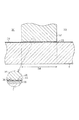
図2は第1領域34及び接着面36近傍を示す要部拡大断面図である。図2に示すよう
に、接着面36は、面粗度Ra=0.1〜10μmと非常に細かい凹凸面である。その凹
部46及び凸部48によって形成される溝部はその深さが浅く微小となっている。尚、第
1領域34には凹部、凸部が形成されておらず、平坦である。
FIG. 2 is an enlarged cross-sectional view of the main part showing the vicinity of the
次に、有機EL素子の製造方法を説明する。
先ず、基板S上の略中央に、公知の方法によって千鳥格子状に配置されるように複数の
画素電極18をパターニングする。続いて、基板S上であって、複数個の画素電極18の
周囲に、複数の画素電極18全体を囲むように酸化珪素(SiO2)をパターニングして
親液性バンク14aを形成する。その後、形成した親液性バンク14a上に、親液性バン
ク14aの一部が基板S中央側に張り出すようにフッ素系樹脂を、例えば高さが1〜2マ
イクロメートルになるようにパターニングして撥液性バンク14bを形成する。これによ
り、基板S上には、複数個の画素電極18の周囲に複数の画素電極18全体を囲むように
バンク14が形成される。この結果、画素電極18が形成された基板S中央には凹状領域
16が形成される。
Next, the manufacturing method of an organic EL element is demonstrated.
First, the plurality of
続いて、凹状領域16内に発光層20を液滴吐出法によって形成する。即ち、発光層2
0を構成する発光材料をキシレンといった所定の溶媒に溶解または分散させて形成された
液状組成物を吐出ヘッドのノズルから吐出させる。このとき、吐出ヘッドに設けられた、
ガイドレールに沿って吐出ヘッドを基板Sに対して相対移動させながら液状組成物を順次
吐出することで凹状領域16内に複数回液状組成物を吐出する。これにより、凹状領域1
6内全面に液状組成物を塗布させる。
Subsequently, the
A liquid composition formed by dissolving or dispersing a light-emitting material constituting 0 in a predetermined solvent such as xylene is ejected from the nozzle of the ejection head. At this time, provided in the ejection head,
By sequentially ejecting the liquid composition while moving the ejection head relative to the substrate S along the guide rail, the liquid composition is ejected into the concave region 16 a plurality of times. Thereby, the concave region 1
The liquid composition is applied to the entire surface of 6.
次に、基板Sを、例えばホットプレート上に載置することによって加熱して液状組成物
中の溶媒を蒸発させ、凹状領域16の全面に発光層20を形成する。
その後、バンク14及び発光層20上に、LiF層、Ca層、Al層等を蒸着方法等に
より積層し、陰極22を形成する。続いて、陰極22全面に光透過性を有する封止ガラス
32を形成する。
Next, the substrate S is heated, for example, by placing it on a hot plate to evaporate the solvent in the liquid composition, and the
Thereafter, a LiF layer, a Ca layer, an Al layer, or the like is laminated on the
詳述すると、封止ガラス32の接着面36は、ショットブラスト装置(図示しない)に
よって、面粗度Ra=0.1〜10μmと非常に細かい凹凸面に形成される。ショットブ
ラスト装置は、圧縮空気等のキャリアガスにより加速された微細な砥粒をノズルから噴出
させ、接着面36に衝突させることにより、加工するものである。これにより、封止ガラ
ス32の接着面36が、所望の面粗度の非常に細かい凹凸面となる。
More specifically, the
次に、基板S上に配線50を形成する。配線50を形成する場合、例えば蒸着やスパッ
タリングなどの所定の手法で基板S上にアルミニウム等の金属膜を成膜する。次いで、フ
ォトリソグラフィ法などの所定の手法を用いて金属膜をパターニングする。こうして、配
線50は第1領域34上を通過するように形成される。
Next, the
そして、基板S上の有機EL素子12上に乾燥剤40を配置する。次に、接着剤38を
基板Sの第1領域34上に塗布する。その後、封止ガラス32の接着面36と基板Sの第
1領域34とを接近させ、基板Sと封止ガラス32とを所定の力で押圧し、第1領域34
と接着面36とを接着剤38を介して貼り合わせる。そして、接着剤38に対して紫外光
を照射する。これによって、接着剤38が硬化し、封止ガラス32は基板Sに対して強固
に接着される。
Then, the desiccant 40 is disposed on the
And the
本実施形態によれば、以下のような効果を得ることができる。
(1)本実施形態によれば、封止ガラス32の接着面36を面粗度Ra=0.1〜10
μmとなる微小な凹凸面にした。この結果、基板S上に形成される外部に引き回される配
線50を形成する際に、その接着剤38を介して封止ガラス32の接着面36と対向する
配線50の形状を特別な形状にすることなく形成することができる。
According to this embodiment, the following effects can be obtained.
(1) According to this embodiment, the
It was made into the micro uneven surface which becomes micrometer. As a result, when forming the
(2)本実施形態によれば、封止ガラス32の接着面36を面粗度Ra=0.1〜10
μmとなる微小な凹凸面にした。この結果、基板S上に形成される外部に引き回される配
線50を形成する際に、その接着剤38を介して封止ガラス32の接着面36と接する配
線50は傷つけられることはない。
(2) According to this embodiment, the
It was made into the micro uneven surface which becomes micrometer. As a result, when forming the
(3)本実施形態によれば、封止ガラス32の接着面36を凹凸面にしたことから、接
着面積が大きくなって大きな密着力で基板Sに対して封止ガラス32を結合させることが
できる。
(3) According to the present embodiment, since the
(4)本実施形態によれば、接着面36は面粗度Ra=0.1〜10μmと微小である
ことから、ショットブラスト等で容易に前記凹部46、凸部48を形成することができる
。しかも、外部空間33と封止空間30までの距離を長くでき、酸素や水分の侵入を防ぐ
ことができる。
(4) According to the present embodiment, since the
(5)本実施形態によれば、封止ガラス32に設けた凹部46、凸部48は微小である
から、素子基板上に封止ガラス32を設置するときの位置合わせが容易である。
○上記実施形態では、凹部46、凸部48を有する接着面36をショットブラスト装置
により製造したが、モールドを備えたナノインプリント装置により製造してもよい。詳述
すると、モールドと封止ガラス32とを封止ガラス32のガラス転移温度以上に加熱する
。次いで、モールドを封止ガラス32に押し付け、一定時間保持する。その後、モールド
と封止ガラス32とを、封止ガラス32のガラス転移温度以下に冷却し、モールドと封止
ガラス32とを離す。これにより、上記実施形態と同様に凹部46、凸部48を有する接
着面36を形成し、同様の効果を得ることができる。また、ナノインプリント装置に限ら
ず、エッチング法、レーザ加工法、掘削法などを用いてもよい。
(5) According to this embodiment, since the
In the above embodiment, the
○上記実施形態では、封止ガラス32の接着面36に面粗度Ra=0.1〜10μmと
なる微小の凹凸面を形成した。これを、封止ガラス32の接着面36に設けずに、基板S
の第1領域34に凹部、凸部による面粗度Ra=0.1〜10μmとなる凹凸としての微
小の凹凸面を設けてもよい。この場合であっても、凹部、凸部は微小であるから、基板S
上の配線の引き回しへの影響を低減でき、配線50への劣化を低減することができる。
In the above embodiment, a minute uneven surface having a surface roughness Ra = 0.1 to 10 μm is formed on the
The
The influence on the routing of the upper wiring can be reduced, and the deterioration of the
○上記実施形態では、主に電子写真プリンタ用の光書き込みヘッド等の電子機器に適用
する場合について説明したが、例えば、マトリックス状の白色の発光素子にカラーフィル
タを組み合わせることによりカラー化を行う表示装置等の電子機器にも使用することが可
能である。
In the above-described embodiment, the case where it is mainly applied to an electronic device such as an optical writing head for an electrophotographic printer has been described. For example, a display that performs colorization by combining a color filter with a white light emitting element in a matrix It can also be used for electronic devices such as devices.
12…有機EL素子、32…封止ガラス、34…第1領域、36…接着面、38…接着
剤、46…凹部、48…凸部、50…配線。
DESCRIPTION OF
Claims (6)
前記素子基板と接着剤を介して接着され、前記複数の表示素子を封止する封止基板とを
備えた有機EL素子において、
前記封止基板の接着面に面粗度Ra=0.1〜10μmの凹凸を形成したことを特徴と
する有機EL素子。 An element substrate including a plurality of display elements;
In an organic EL element comprising a sealing substrate that is bonded to the element substrate via an adhesive and seals the plurality of display elements.
An organic EL element, wherein irregularities having a surface roughness Ra = 0.1 to 10 μm are formed on the adhesive surface of the sealing substrate.
前記素子基板の接着面は平坦であることを特徴とする有機EL素子。 The organic EL device according to claim 1,
An organic EL element, wherein an adhesive surface of the element substrate is flat.
前記素子基板と接着剤を介して接着され、前記複数の表示素子を封止する封止基板とを
備えた有機EL素子において、
前記素子基板の接着面に面粗度がRa=0.1〜10μmの凹凸を形成したことを特徴
とする有機EL素子。 An element substrate including a plurality of display elements;
In an organic EL element comprising a sealing substrate that is bonded to the element substrate via an adhesive and seals the plurality of display elements.
An organic EL element, wherein unevenness having a surface roughness Ra = 0.1 to 10 μm is formed on the bonding surface of the element substrate.
前記封止基板の接着面は平坦であることを特徴とする有機EL素子。 The organic EL device according to claim 3,
An organic EL element, wherein an adhesive surface of the sealing substrate is flat.
前記接着面における凹凸は前記表示素子を囲むように環状に形成されていることを特徴
とする有機EL素子。 In the organic EL element according to any one of claims 1 to 4,
The organic EL element, wherein the unevenness on the adhesive surface is formed in an annular shape so as to surround the display element.
器。 An electronic apparatus comprising the organic EL element according to claim 1.
Priority Applications (1)
| Application Number | Priority Date | Filing Date | Title |
|---|---|---|---|
| JP2006250402A JP2008071663A (en) | 2006-09-15 | 2006-09-15 | Organic EL elements, electronic devices |
Applications Claiming Priority (1)
| Application Number | Priority Date | Filing Date | Title |
|---|---|---|---|
| JP2006250402A JP2008071663A (en) | 2006-09-15 | 2006-09-15 | Organic EL elements, electronic devices |
Publications (1)
| Publication Number | Publication Date |
|---|---|
| JP2008071663A true JP2008071663A (en) | 2008-03-27 |
Family
ID=39293066
Family Applications (1)
| Application Number | Title | Priority Date | Filing Date |
|---|---|---|---|
| JP2006250402A Withdrawn JP2008071663A (en) | 2006-09-15 | 2006-09-15 | Organic EL elements, electronic devices |
Country Status (1)
| Country | Link |
|---|---|
| JP (1) | JP2008071663A (en) |
Cited By (1)
| Publication number | Priority date | Publication date | Assignee | Title |
|---|---|---|---|---|
| KR20120137264A (en) | 2011-06-09 | 2012-12-20 | 가부시키가이샤 한도오따이 에네루기 켄큐쇼 | Lighting device and method for manufacturing the same |
-
2006
- 2006-09-15 JP JP2006250402A patent/JP2008071663A/en not_active Withdrawn
Cited By (4)
| Publication number | Priority date | Publication date | Assignee | Title |
|---|---|---|---|---|
| KR20120137264A (en) | 2011-06-09 | 2012-12-20 | 가부시키가이샤 한도오따이 에네루기 켄큐쇼 | Lighting device and method for manufacturing the same |
| JP2013016469A (en) * | 2011-06-09 | 2013-01-24 | Semiconductor Energy Lab Co Ltd | Lighting device and manufacturing method of the same |
| US8698190B2 (en) | 2011-06-09 | 2014-04-15 | Semiconductor Energy Laboratory Co., Ltd. | Lighting device and method for manufacturing the same |
| KR101869232B1 (en) | 2011-06-09 | 2018-06-21 | 가부시키가이샤 한도오따이 에네루기 켄큐쇼 | Lighting device and method for manufacturing the same |
Similar Documents
| Publication | Publication Date | Title |
|---|---|---|
| CN100364133C (en) | Display device and manufacturing method thereof | |
| JP4438710B2 (en) | Mask, mask chip, mask manufacturing method, and mask chip manufacturing method | |
| CN101257036A (en) | Organic EL display device | |
| KR101274785B1 (en) | organic electro-luminescence display device and method for fabricating the same | |
| JP2004139987A (en) | Encapsulation of front-emitting organic light-emitting diode panel | |
| KR20080087257A (en) | Organic electroluminescent display and manufacturing method | |
| US10367170B2 (en) | Light emitting device with irregularities located on a first light transmissive substrate and a second light transmissive substrate | |
| JP2010277944A (en) | Organic EL display panel and manufacturing method thereof | |
| JP2013089475A (en) | Light-emitting display device and method for manufacturing the same | |
| KR100544133B1 (en) | Actively Driven Flat Panel Display | |
| TWI679716B (en) | Method of manufacturing flexible electronic device | |
| KR100799813B1 (en) | Masks, mask manufacturing methods, film formation methods, electro-optical devices manufacturing methods and electronic devices | |
| WO2019215832A1 (en) | Method and apparatus for manufacturing flexible light-emitting device | |
| KR20090073478A (en) | Organic light emitting display device and manufacturing method | |
| CN1630438A (en) | Mask and manufacturing method thereof, organic electroluminescent device and manufacturing method thereof, electronic device | |
| JP2011048915A (en) | Manufacturing device of luminescent panel, manufacturing method of the same and electronic apparatus | |
| KR20060020031A (en) | Laser thermal transfer device | |
| JP2008189990A (en) | DEPOSITION MASK AND METHOD FOR PRODUCING DEPOSITION MASK | |
| JP2008071663A (en) | Organic EL elements, electronic devices | |
| JP2014041740A (en) | Display device and manufacturing method of the same | |
| KR100567223B1 (en) | A flat display device and a method for producting the same | |
| TWI635635B (en) | Element structure and method of manufacturing the same | |
| JP2007044582A (en) | Surface treatment method, electro-optical device manufacturing method, and electro-optical device | |
| KR100815761B1 (en) | Manufacturing method of organic electroluminescent display | |
| CN1905243A (en) | Method for manufacturing a mask and an organic EL element and an organic EL printer |
Legal Events
| Date | Code | Title | Description |
|---|---|---|---|
| A300 | Application deemed to be withdrawn because no request for examination was validly filed |
Free format text: JAPANESE INTERMEDIATE CODE: A300 Effective date: 20091201 |