JP2008061176A - Level shifter apparatus - Google Patents
Level shifter apparatus Download PDFInfo
- Publication number
- JP2008061176A JP2008061176A JP2006238832A JP2006238832A JP2008061176A JP 2008061176 A JP2008061176 A JP 2008061176A JP 2006238832 A JP2006238832 A JP 2006238832A JP 2006238832 A JP2006238832 A JP 2006238832A JP 2008061176 A JP2008061176 A JP 2008061176A
- Authority
- JP
- Japan
- Prior art keywords
- signal
- level
- inverter
- output
- circuit
- Prior art date
- Legal status (The legal status is an assumption and is not a legal conclusion. Google has not performed a legal analysis and makes no representation as to the accuracy of the status listed.)
- Withdrawn
Links
Images


Classifications
-
- H—ELECTRICITY
- H03—ELECTRONIC CIRCUITRY
- H03K—PULSE TECHNIQUE
- H03K5/00—Manipulating of pulses not covered by one of the other main groups of this subclass
- H03K5/156—Arrangements in which a continuous pulse train is transformed into a train having a desired pattern
- H03K5/1565—Arrangements in which a continuous pulse train is transformed into a train having a desired pattern the output pulses having a constant duty cycle
-
- H—ELECTRICITY
- H03—ELECTRONIC CIRCUITRY
- H03K—PULSE TECHNIQUE
- H03K19/00—Logic circuits, i.e. having at least two inputs acting on one output; Inverting circuits
- H03K19/0175—Coupling arrangements; Interface arrangements
- H03K19/0185—Coupling arrangements; Interface arrangements using field effect transistors only
- H03K19/018507—Interface arrangements
- H03K19/018521—Interface arrangements of complementary type, e.g. CMOS
- H03K19/018528—Interface arrangements of complementary type, e.g. CMOS with at least one differential stage
-
- H—ELECTRICITY
- H03—ELECTRONIC CIRCUITRY
- H03K—PULSE TECHNIQUE
- H03K3/00—Circuits for generating electric pulses; Monostable, bistable or multistable circuits
- H03K3/02—Generators characterised by the type of circuit or by the means used for producing pulses
- H03K3/353—Generators characterised by the type of circuit or by the means used for producing pulses by the use, as active elements, of field-effect transistors with internal or external positive feedback
- H03K3/356—Bistable circuits
- H03K3/356104—Bistable circuits using complementary field-effect transistors
- H03K3/356113—Bistable circuits using complementary field-effect transistors using additional transistors in the input circuit
- H03K3/35613—Bistable circuits using complementary field-effect transistors using additional transistors in the input circuit the input circuit having a differential configuration
Abstract
Description
本発明は、入力信号を所定分レベルシフトして出力するレベルシフト装置において、入力信号のデューティ比に対する出力信号のデューティ比の誤差の軽減を図る技術に関する。 The present invention relates to a technique for reducing an error of a duty ratio of an output signal with respect to a duty ratio of an input signal in a level shift apparatus that outputs an input signal by shifting the level by a predetermined amount.
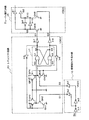
入力信号を所定分レベルシフトして出力する従来のレベルシフト装置の構成を図4に示す。このレベルシフト装置は、低電位電源VDD1を電圧源とする相補信号生成回路10と、高電位電源VDD2を電圧源とするレベルシフト回路20とで構成され、低電位電源VDD1の入力信号Sinを高電位電圧源VDD2の出力信号にレベルシフトするものである。In1〜In4は相補信号生成回路10におけるインバータ、QP1〜QP4はレベルシフト回路20におけるPMOSトランジスタ、QN1〜QN4はNMOSトランジスタ、LHはR-Sラッチ回路、In5,In6,In8はインバータである。
FIG. 4 shows the configuration of a conventional level shift apparatus that outputs an input signal after shifting the level by a predetermined amount. This level shift device includes a complementary
図4に示すレベルシフト装置の動作を図5のタイミングチャートを用いて説明する。 The operation of the level shifter shown in FIG. 4 will be described using the timing chart of FIG.
レベルシフト装置に対する入力信号Sinを図5(a)に示す。この入力信号Sinは、まず相補信号生成回路10のインバータIn1を介してインバータIn2,In3に供給される。さらにインバータIn3を介してインバータIn4に供給される。このとき、インバータIn2の出力信号S1は図5(b)に示すように入力信号に対して所定の遅延τ1をもつ正転信号となり、インバータIn4の出力信号S2は図5(c)に示すように入力信号に対して所定の遅延τ2 をもつ反転信号となる。
An input signal Sin for the level shift device is shown in FIG. This input signal Sin is first supplied to the inverters In2 and In3 via the inverter In1 of the complementary
インバータIn2の出力信号S1は、レベルシフト回路20のNMOSトランジスタQN2のゲートに供給される。図5(b)に示すように時刻T2 においてNMOSトランジスタQN2のゲートにハイレベルの信号が供給されると、NMOSトランジスタQN2はオン状態となる。このとき、インバータIn5からの帰還信号(信号S5の反転信号)はハイレベルであるため、NMOSトランジスタQN1はオン状態となり、PMOSトランジスタQP1はオフ状態となる。また、PMOSトランジスタQP2のゲートは接地されているため、常にオン状態となるが、PMOSトランジスタQP2のオン抵抗はNMOSトランジスタQN2,QN1よりも高抵抗に設定されている。これにより、時刻T2 において、NMOSトランジスタQN2のゲートにハイレベルの信号が供給されると、R-Sラッチ回路LHのNAND回路N1への入力信号S3は、図5(d)に示すようにローレベルとなる。このため、NAND回路N1の出力信号S5は、インバータIn5のゲート容量により、図5(f)の時刻T2より徐々にハイレベルとなる。この出力信号S5は、インバータIn5に供給され、極性を反転してPMOSトランジスタQP1、NMOSトランジスタQN1のゲートに供給される。 The output signal S1 of the inverter In2 is supplied to the gate of the NMOS transistor QN2 of the level shift circuit 20. When a high level signal to the gate of the NMOS transistor QN2 is supplied at time T 2, As illustrated in FIG 5 (b), the NMOS transistor QN2 is turned on. At this time, since the feedback signal from the inverter In5 (inversion signal of the signal S5) is at a high level, the NMOS transistor QN1 is turned on and the PMOS transistor QP1 is turned off. Since the gate of the PMOS transistor QP2 is grounded, the PMOS transistor QP2 is always turned on, but the on-resistance of the PMOS transistor QP2 is set to be higher than that of the NMOS transistors QN2 and QN1. Thus, at time T 2, when a high-level signal to the gate of the NMOS transistor QN2 is supplied, the input signal S3 to R-S NAND circuit N1 of the latch circuit LH, as shown in FIG. 5 (d) Become low level. Therefore, the output signal S5 of the NAND circuit N1, the gate capacitance of the inverter In5, gradually becomes high-level from the time T 2 of the FIG. 5 (f). This output signal S5 is supplied to the inverter In5, inverted in polarity, and supplied to the gates of the PMOS transistor QP1 and the NMOS transistor QN1.
すなわち、R-Sラッチ回路LHのNAND回路N1に入力される入力信号S3の立ち下がりエッジは、所定の遅延の後、PMOSトランジスタQP1、NMOSトランジスタQN1のゲート入力の立ち下がりエッジとして帰還される。この帰還信号により、PMOSトランジスタQP1はオン状態、NMOSトランジスタQN1はオフ状態となり、R-Sラッチ回路LHのNAND回路N1への入力信号S3はハイレベルとなる。このとき、NAND回路N1の他方の入力信号S6はローレベルとなっているため、NAND回路N1の出力信号S5はハイレベルに保持される。 That is, the falling edge of the input signal S3 input to the NAND circuit N1 of the R-S latch circuit LH is fed back as a falling edge of the gate inputs of the PMOS transistor QP1 and the NMOS transistor QN1 after a predetermined delay. By this feedback signal, the PMOS transistor QP1 is turned on, the NMOS transistor QN1 is turned off, and the input signal S3 to the NAND circuit N1 of the RS latch circuit LH becomes high level. At this time, since the other input signal S6 of the NAND circuit N1 is at a low level, the output signal S5 of the NAND circuit N1 is held at a high level.
一方、インバータIn4の出力信号S2は、レベルシフト回路20のNMOSトランジスタQN4のゲートに供給される。図5(c)に示すように時刻T12において、NMOSトランジスタQN4のゲートにハイレベルの信号が供給されると、NMOSトランジスタQN4はオン状態となる。このとき、インバータIn6からの帰還信号(信号S6の反転信号)はハイレベルであるため、NMOSトランジスタQN3はオン状態となり、PMOSトランジスタQP4はオフ状態となる。また、PMOSトランジスタQP3のゲートは接地されているため、常にオン状態となるが、PMOSトランジスタQP3のオン抵抗はNMOSトランジスタQN4,QN3よりも高抵抗に設定されている。これにより、時刻T12において、NMOSトランジスタQN4のゲートにハイレベルの信号が供給されると、R-Sラッチ回路LHのNAND回路N2への入力信号S4は、図5(e)に示すようにローレベルとなる。このため、NAND回路N2の出力信号S6は、インバータIn6のゲート容量により、図5(g)の時刻T12より徐々にハイレベルとなる。この出力信号S6は、インバータIn6に供給され、極性を反転してPMOSトランジスタQP4、NMOSトランジスタQN3のゲートに供給される。 On the other hand, the output signal S2 of the inverter In4 is supplied to the gate of the NMOS transistor QN4 of the level shift circuit 20. At time T 12, as shown in FIG. 5 (c), when a high-level signal to the gate of the NMOS transistor QN4 is supplied, the NMOS transistor QN4 is turned on. At this time, since the feedback signal from the inverter In6 (inversion signal of the signal S6) is at a high level, the NMOS transistor QN3 is turned on and the PMOS transistor QP4 is turned off. Since the gate of the PMOS transistor QP3 is grounded, the PMOS transistor QP3 is always turned on, but the on-resistance of the PMOS transistor QP3 is set to be higher than that of the NMOS transistors QN4 and QN3. Thus, at time T 12, the signal of high level is supplied to the gate of the NMOS transistor QN4, input signal S4 to the NAND circuit N2 of the R-S latch circuit LH, as shown in FIG. 5 (e) Become low level. Therefore, the output signal S6 of the NAND circuit N2, the gate capacitance of the inverter In6, gradually becomes high-level from the time T 12 in FIG. 5 (g). This output signal S6 is supplied to the inverter In6, inverted in polarity, and supplied to the gates of the PMOS transistor QP4 and the NMOS transistor QN3.
すなわち、R-Sラッチ回路LHのNAND回路N2に入力される入力信号S4立ち下がりエッジは、所定の遅延の後、PMOSトランジスタQP4、NMOSトランジスタQN3のゲート入力の立ち下がりエッジとして帰還される。この帰還信号により、PMOSトランジスタQP4はオン状態、NMOSトランジスタQN3はオフ状態となり、R-Sラッチ回路LHのNAND回路N2への入力信号S4はハイレベルとなる。このとき、NAND回路N2の他方の入力信号S5はローレベルとなっているため、NAND回路N2の出力信号S6はハイレベルに保持される。 That is, the falling edge of the input signal S4 input to the NAND circuit N2 of the RS latch circuit LH is fed back as the falling edge of the gate inputs of the PMOS transistor QP4 and the NMOS transistor QN3 after a predetermined delay. By this feedback signal, the PMOS transistor QP4 is turned on, the NMOS transistor QN3 is turned off, and the input signal S4 to the NAND circuit N2 of the RS latch circuit LH becomes high level. At this time, since the other input signal S5 of the NAND circuit N2 is at a low level, the output signal S6 of the NAND circuit N2 is held at a high level.
したがって、NMOSトランジスタQN2,QN4のゲートにハイレベルの信号が供給されると、所定の遅延の後、NAND回路N1,N2の出力信号S5,S6はハイレベルとなる。NAND回路N1,N2は互いの出力を他方の入力に帰還する接続であるため、時刻T3 においてNAND回路N1の出力信号S5がハイレベルになると、NAND回路N2の出力信号S6は、図5(g)のようにインバータIn6のゲート容量により徐々にローレベルになる。また、時刻T13においてNAND回路N2の出力信号S6がハイレベルになると、NAND回路N1の出力信号S5は、図5(f)のように、インバータIn5のゲート容量により徐々にローレベルになる。 Therefore, when a high level signal is supplied to the gates of the NMOS transistors QN2 and QN4, the output signals S5 and S6 of the NAND circuits N1 and N2 become high level after a predetermined delay. Since NAND circuits N1, N2 is connected to the feedback output of each other to the other input, the output signal S5 of the NAND circuit N1 becomes high level at time T 3, the output signal S6 of the NAND circuit N2, 5 ( As shown in g), the level gradually becomes low due to the gate capacitance of the inverter In6. When the output signal S6 of the NAND circuit N2 becomes high level at time T 13, the output signal S5 of the NAND circuit N1, as shown in FIG. 5 (f), the level gradually due to the gate capacitance of the inverter In5.
NAND回路N2の出力信号S6は、インバータIn8に供給され、極性を反転して出力される。したがって、インバータIn8の出力であるレベルシフト出力信号S8は図5(h)のようになる。このレベルシフト出力信号S8の立ち上がりエッジは、図5(d)で示されるNAND回路N1の入力信号S3の立ち下がりエッジに対して所定の遅延τP をもつ。一方、レベルシフト出力信号S8の立ち下がりエッジは、図5(e)で示されるNAND回路N2の入力信号S4の立ち下がりエッジに対して所定の遅延τR をもつ。 The output signal S6 of the NAND circuit N2 is supplied to the inverter In8 and output with the polarity inverted. Accordingly, the level shift output signal S8 that is the output of the inverter In8 is as shown in FIG. The rising edge of the level shift output signal S8 has a predetermined delay τ P with respect to the falling edge of the input signal S3 of the NAND circuit N1 shown in FIG. On the other hand, the falling edge of the level shift output signal S8 has a predetermined delay τ R with respect to the falling edge of the input signal S4 of the NAND circuit N2 shown in FIG.
ここで、レベルシフト出力信号S8のハイレベル期間TH とローレベル期間TL を考える。 Here, a high level period T H and a low level period T L of the level shift output signal S8 are considered.
相補信号生成回路10への入力信号Sinのデューティ比を50%とし、その半波長をT0 とする。
The duty ratio of the input signal Sin to the complementary
ハイレベル期間TH は、
TH =T0 −(τ1 +τP )+(τ2 +τR )
ローレベル期間TL は、
TL =2×T0−TH
したがって、TL >TH として、ローレベル期間TL とハイレベル期間TH との差分ΔTは、
ΔT=TL −TH =2{(τ1 −τ2 )+(τP −τR )}
となる。ここで、例えば、τ2 =2×τ1 、τP =2×τR とすると、
ΔT=2(τR −τ1 )
となる。
The high level period TH is
T H = T 0 − (τ 1 + τ P ) + (τ 2 + τ R )
The low level period T L is
T L = 2 × T 0 −T H
Therefore, when T L > T H , the difference ΔT between the low level period T L and the high level period T H is:
ΔT = T L −T H = 2 {(τ 1 −τ 2 ) + (τ P −τ R )}
It becomes. For example, if τ 2 = 2 × τ 1 and τ P = 2 × τ R ,
ΔT = 2 (τ R −τ 1 )
It becomes.
見方を変えて、インバータIn4の出力信号S2を基準に考えると、次のようになる。レベルシフト出力信号S8の立ち下がりエッジ(時刻T13)は、出力信号S2の立ち上がりエッジ(時刻T12)からτR だけ遅延している。インバータIn2の出力信号S1は入力信号Sinに対してインバータIn2による時間τ1だけ遅延している。インバータIn4の出力信号S2は入力信号Sinに対してインバータIn3,In4による時間τ1 ′だけ遅延している。ここで、インバータIn2,In3,In4の特性が同じものとして、τ1′=τ1 とする。 From a different perspective, the output signal S2 of the inverter In4 is considered as a reference as follows. The falling edge (time T 13 ) of the level shift output signal S8 is delayed by τ R from the rising edge (time T 12 ) of the output signal S2. The output signal S1 of the inverter In2 is delayed from the input signal Sin by a time τ 1 by the inverter In2. The output signal S2 of the inverter In4 is delayed with respect to the input signal Sin by the time τ 1 ′ by the inverters In3 and In4. Here, assuming that the characteristics of the inverters In2, In3, In4 are the same, τ 1 ′ = τ 1 .
レベルシフト出力信号S8の立ち上がりエッジ(時刻T4 )は、出力信号S2の立ち下がりエッジ(時刻T2′)から、
τP −τ1 ′=τP −τ1 =2τR −τ1
だけ遅延している。すなわち、レベルシフト出力信号S8の立ち上がりエッジの出力信号S2からの遅延が(2τR −τ1 )であるのに対して、レベルシフト出力信号S8の立ち下がりエッジの出力信号S2からの遅延は上記のようにτR であるので、レベルシフト出力信号S8のハイレベル期間TH は、入力信号Sinの半波長T0 から、(2τR −τ1 )−τR =τR−τ1 だけ短いものとなる。一方、レベルシフト出力信号S8のローレベル期間TL は、入力信号Sinの半波長T0から、(τR −τ1 )だけ長いものとなる。それゆえに、ローレベル期間TL とハイレベル期間THとの差分ΔTは、
ΔT=(τR −τ1 )×2=2(τR −τ1 )
となり、上記の説明と一致している。
The rising edge (time T 4 ) of the level shift output signal S8 is derived from the falling edge (time T 2 ') of the output signal S2.
τ P −τ 1 ′ = τ P −τ 1 = 2τ R −τ 1
Only delayed. That is, the delay from the output signal S2 of the rising edge of the level shift output signal S8 is (2τ R −τ 1 ), whereas the delay from the output signal S2 of the falling edge of the level shift output signal S8 is since in tau R as the high-level period T H of the level shift output signal S8 from the half wavelength T 0 of the input signal Sin, (2τ R -τ 1) -τ R = τ R -
ΔT = (τ R −τ 1 ) × 2 = 2 (τ R −τ 1 )
And is consistent with the above description.
τR ≠τ1 であるので、ローレベル期間TL とハイレベル期間TH との差分ΔTはゼロとはならない。すなわち、入力信号Sinのデューティ比に対してレベルシフト出力信号S8のデューティ比は誤差を生じている。
このように、従来回路においては、相補信号生成回路において生成される2本の信号の遅延差と、レベルシフト回路で使用されるR-Sラッチ回路の信号伝播による遅延とにより、デューティ比の変動が発生するという問題があった。 As described above, in the conventional circuit, the duty ratio varies due to the delay difference between the two signals generated in the complementary signal generation circuit and the delay due to the signal propagation of the RS latch circuit used in the level shift circuit. There was a problem that occurred.
本発明は、このような事情に鑑みて創作したものであり、入力信号のデューティ比に対する出力信号のデューティ比の誤差が少ないレベルシフト装置を提供することを目的としている。 The present invention was created in view of such circumstances, and an object of the present invention is to provide a level shift device with a small error in the duty ratio of the output signal with respect to the duty ratio of the input signal.
本発明によるレベルシフト装置は、1本の入力信号を電圧レベル変換し、電圧レベル変換後の信号を出力するレベルシフト回路と、前記レベルシフト回路の出力信号を入力して、前記入力信号のデューティに対する前記レベルシフト回路の出力信号のデューティのずれを相殺するデューティ補正回路とを備えたものである。 A level shift apparatus according to the present invention converts a voltage level of one input signal, outputs a signal after voltage level conversion, inputs the output signal of the level shift circuit, and outputs the duty of the input signal. And a duty correction circuit for canceling out a duty shift of the output signal of the level shift circuit.
この構成においては、レベルシフト回路の後段に、入力信号のデューティに対するレベルシフト回路の出力信号のデューティのずれを相殺するデューティ補正回路を設けたので、入力信号のデューティ比に対するレベルシフト出力信号のデューティ比の誤差が軽減される。 In this configuration, since the duty correction circuit that cancels the deviation of the duty of the output signal of the level shift circuit with respect to the duty of the input signal is provided at the subsequent stage of the level shift circuit, the duty of the level shift output signal with respect to the duty ratio of the input signal Ratio error is reduced.
より具体的レベルで、本発明のレベルシフト装置は、1本の入力信号を電圧レベル変換し、電圧レベル変換後の信号をR-Sラッチ回路によって2本の信号として出力するレベルシフト回路と、このレベルシフト回路の次段にあって、次のような回路構成を有するデューティ補正回路とを備えたものである。そのデューティ補正回路は、前記レベルシフト回路における前記R-Sラッチ回路からの2本の出力信号をそれぞれ第1、第2の入力信号とし、前記第1の入力信号がゲートに接続され、ソースが接地される第1のNMOSトランジスタと、前記第2の入力信号がゲートに接続され、ソースが接地される第2のNMOSトランジスタと、入力端子が前記第2のNMOSトランジスタのドレインに接続され、出力端子が前記第1のNMOSトランジスタのドレインに接続される第1のインバータと、入力端子が前記第1のNMOSトランジスタのドレインに接続され、出力端子が前記第2のNMOSトランジスタのドレインに接続される第2のインバータと、前記第1のインバータの出力信号を入力信号としレベルシフトの出力とする第1のバッファと、前記第2のインバータの出力信号を入力信号とする第2のバッファから構成されている。 In a more specific level, the level shift device of the present invention performs a voltage level conversion on one input signal and outputs a signal after the voltage level conversion as two signals by an RS latch circuit; In the next stage of the level shift circuit, a duty correction circuit having the following circuit configuration is provided. The duty correction circuit uses two output signals from the RS latch circuit in the level shift circuit as first and second input signals, respectively, the first input signal is connected to the gate, and the source is A grounded first NMOS transistor, the second input signal is connected to a gate, a source is grounded a second NMOS transistor, an input terminal is connected to a drain of the second NMOS transistor, and an output A first inverter having a terminal connected to the drain of the first NMOS transistor; an input terminal connected to the drain of the first NMOS transistor; and an output terminal connected to the drain of the second NMOS transistor. The first inverter that uses the output signal of the second inverter and the first inverter as an input signal and outputs the level shift. And a second buffer having the output signal of the second inverter as an input signal.
また、上記構成において導電型をNMOSからPMOSに置き換えたものとして、本発明によるレベルシフト装置は、1本の入力信号を電圧レベル変換し、電圧レベル変換後の信号をR-Sラッチ回路によって2本の信号として出力するレベルシフト回路と、このレベルシフト回路の次段にあって、次のような回路構成を有するデューティ補正回路とを備えたものである。そのデューティ補正回路は、前記レベルシフト回路における前記R-Sラッチ回路からの2本の出力信号をそれぞれ第1、第2の入力信号とし、前記第1の入力信号がゲートに接続され、ソースが高電位電源に接続される第1のPMOSトランジスタと、前記第2の入力信号がゲートに接続され、ソースが高電位電源に接続される第2のPMOSトランジスタと、入力端子が前記第2のPMOSトランジスタのドレインに接続され、出力端子が前記第1のPMOSトランジスタのドレインに接続される第1のインバータと、入力端子が前記第1のPMOSトランジスタのドレインに接続され、出力端子が前記第2のPMOSトランジスタのドレインに接続される第2のインバータと、前記第1のインバータの出力信号を入力信号としレベルシフトの出力とする第1のバッファと、前記第2のインバータの出力信号を入力信号とする第2のバッファから構成されている。 Further, assuming that the conductivity type is replaced from NMOS to PMOS in the above configuration, the level shift device according to the present invention converts one input signal to a voltage level, and the signal after the voltage level conversion is converted to 2 by an R-S latch circuit. It comprises a level shift circuit that outputs as a book signal and a duty correction circuit that is in the next stage of this level shift circuit and has the following circuit configuration. The duty correction circuit uses two output signals from the RS latch circuit in the level shift circuit as first and second input signals, respectively, the first input signal is connected to the gate, and the source is A first PMOS transistor connected to a high-potential power source, a second PMOS transistor whose second input signal is connected to the gate, a source connected to the high-potential power source, and an input terminal connected to the second PMOS transistor A first inverter connected to the drain of the transistor, an output terminal connected to the drain of the first PMOS transistor, an input terminal connected to the drain of the first PMOS transistor, and an output terminal connected to the second PMOS transistor; A second inverter connected to the drain of the PMOS transistor and a level shifter using the output signal of the first inverter as an input signal. And a second buffer using the output signal of the second inverter as an input signal.
デューティ補正回路は、レベルシフト回路のR-Sラッチ回路から出力される従来のレベルシフト出力信号に相当する信号とは別に生成出力される矩形波信号を利用して従来のレベルシフト出力信号に相当する信号のデューティ比を補正するものである。具体的には、従来のレベルシフト出力信号に相当する信号の立ち下がりエッジを矩形波信号の立ち上がりエッジまで遅らせて、レベルシフト出力信号の立ち下がりエッジを規定する。一方、従来のレベルシフト出力信号に相当する信号の立ち上がりエッジを第1および第2のインバータの逆並列接続で遅延させて、レベルシフト出力信号の立ち上がりエッジを規定する。このときの遅延関係の調整により、レベルシフト出力信号のハイレベル期間とローレベル期間との差分を減少させ、入力信号のデューティ比に対する出力信号のデューティ比の誤差を軽減する。 The duty correction circuit corresponds to a conventional level shift output signal using a rectangular wave signal generated and output separately from the signal corresponding to the conventional level shift output signal output from the RS latch circuit of the level shift circuit. The duty ratio of the signal to be corrected is corrected. Specifically, the falling edge of the signal corresponding to the conventional level shift output signal is delayed until the rising edge of the rectangular wave signal to define the falling edge of the level shift output signal. On the other hand, the rising edge of the signal corresponding to the conventional level shift output signal is delayed by the antiparallel connection of the first and second inverters to define the rising edge of the level shift output signal. By adjusting the delay relationship at this time, the difference between the high level period and the low level period of the level shift output signal is reduced, and the error of the duty ratio of the output signal with respect to the duty ratio of the input signal is reduced.
上記構成のレベルシフト装置において、前記デューティ補正回路の前記第1の入力信号がハイレベル、前記第2の入力信号がローレベルのとき、前記第1のバッファの出力がローレベル、前記第2のバッファの出力がハイレベルとなり、前記第1の入力信号がローレベル、前記第2の入力信号がハイレベルのとき、前記第1のバッファの出力がハイレベル、前記第2のバッファの出力がローレベルとなり、前記第1、第2の入力信号がローレベルのとき、前記第1、第2のバッファの出力は保持されるように構成されているという態様がある。 In the level shift device having the above configuration, when the first input signal of the duty correction circuit is high level and the second input signal is low level, the output of the first buffer is low level, When the output of the buffer becomes high level, the first input signal is low level, and the second input signal is high level, the output of the first buffer is high level, and the output of the second buffer is low When the first and second input signals are at the low level, the outputs of the first and second buffers are configured to be held.
ここでは、第1、第2の入力信号の立ち上がりエッジに同期して、第1、第2のバッファ出力のうち一方を、または両方を出力信号とする。デューティ補正回路の両入力が同時にハイレベルになることはない。 Here, one or both of the first and second buffer outputs are set as output signals in synchronization with the rising edges of the first and second input signals. Both inputs of the duty correction circuit do not become high level at the same time.
本発明によれば、レベルシフト回路のR-Sラッチ回路から出力される2つの信号を利用して出力信号のデューティ比を補正するデューティ補正回路を設け、立ち下がりエッジと立ち上がりエッジの位相を調整することにより、レベルシフト出力信号のハイレベル期間とローレベル期間との差分を減少させ、入力信号のデューティ比に対する出力信号のデューティ比の誤差を軽減することができる。 According to the present invention, a duty correction circuit that corrects the duty ratio of the output signal using two signals output from the RS latch circuit of the level shift circuit is provided, and the phase of the falling edge and the rising edge is adjusted. By doing so, the difference between the high level period and the low level period of the level shift output signal can be reduced, and the error of the duty ratio of the output signal with respect to the duty ratio of the input signal can be reduced.
以下、本発明にかかわるレベルシフト装置の実施の形態を図面を用いて詳細に説明する。 Embodiments of a level shift apparatus according to the present invention will be described below in detail with reference to the drawings.
(実施の形態1)
図1は本発明の実施の形態1におけるレベルシフト装置の構成を示す回路図である。
(Embodiment 1)
FIG. 1 is a circuit diagram showing a configuration of a level shift apparatus according to
本実施の形態のレベルシフト装置は、低電位電源VDD1を電圧源とする相補信号生成回路10と、高電位電源VDD2を電圧源とするレベルシフト回路20と、高電位電源VDD2を電圧源とするデューティ補正回路30とで構成されている。
The level shift device of this embodiment includes a complementary
相補信号生成回路10は、4つのインバータIn1,In2,In3,In4で構成されている。
The complementary
第1のインバータIn1の出力は第2、第3のインバータIn2,In3の入力端子に接続され、インバータIn3の出力は第4のインバータIn4の入力端子に接続されている。 The output of the first inverter In1 is connected to the input terminals of the second and third inverters In2 and In3, and the output of the inverter In3 is connected to the input terminal of the fourth inverter In4.
レベルシフト回路20は、4つのPMOSトランジスタQP1,QP2,QP3,QP4と、4つのNMOSトランジスタQN1,QN2,QN3,QN4と、R-Sラッチ回路LHと、4つのインバータIn5,In6,In7,In8とで構成されている。 The level shift circuit 20 includes four PMOS transistors QP1, QP2, QP3, QP4, four NMOS transistors QN1, QN2, QN3, QN4, an RS latch circuit LH, and four inverters In5, In6, In7, In8. It consists of and.
PMOSトランジスタQP1,QP2は、各ソースが高電位電源に接続されており、各ドレインがNMOSトランジスタQN2のドレインに接続されている。また、PMOSトランジスタQP1のゲートはインバータIn5の出力端子に接続され、PMOSトランジスタQP2のゲートは接地されている。 Each source of the PMOS transistors QP1 and QP2 is connected to the high potential power source, and each drain is connected to the drain of the NMOS transistor QN2. The gate of the PMOS transistor QP1 is connected to the output terminal of the inverter In5, and the gate of the PMOS transistor QP2 is grounded.
PMOSトランジスタQP3,QP4は、各ソースが高電位電源に接続されており、各ドレインがNMOSトランジスタQN4のドレインに接続されている。また、PMOSトランジスタQP4のゲートはインバータIn6の出力端子に接続され、PMOSトランジスタQP3のゲートは接地されている。 The sources of the PMOS transistors QP3 and QP4 are connected to the high potential power source, and the drains are connected to the drain of the NMOS transistor QN4. The gate of the PMOS transistor QP4 is connected to the output terminal of the inverter In6, and the gate of the PMOS transistor QP3 is grounded.
NMOSトランジスタQN2のソースはNMOSトランジスタQN1のドレインに接続され、NMOSトランジスタQN1のソースは接地されている。また、NMOSトランジスタQN2のゲートは相補信号生成回路10のインバータIn2の出力端子に接続され、NMOSトランジスタQN1のゲートはインバータIn5の出力端子に接続されている。
The source of the NMOS transistor QN2 is connected to the drain of the NMOS transistor QN1, and the source of the NMOS transistor QN1 is grounded. The gate of the NMOS transistor QN2 is connected to the output terminal of the inverter In2 of the complementary
NMOSトランジスタQN4のソースはNMOSトランジスタQN3のドレインに接続され、NMOSトランジスタQN3のソースは接地されている。また、NMOSトランジスタQN4のゲートは相補信号生成回路10のインバータIn4の出力端子に接続され、NMOSトランジスタQN3のゲートはインバータIn6の出力端子に接続されている。
The source of the NMOS transistor QN4 is connected to the drain of the NMOS transistor QN3, and the source of the NMOS transistor QN3 is grounded. The gate of the NMOS transistor QN4 is connected to the output terminal of the inverter In4 of the complementary
R-Sラッチ回路LHは、第1、第2のNAND回路N1,N2で構成されており、NAND回路N1の出力信号S5はNAND回路N2の一方の入力に、NAND回路N2の出力信号S6はNAND回路N1の一方の入力に帰還する接続となっている。NAND回路N1の他方の入力端子はNMOSトランジスタQN2のドレインに接続され、NAND回路N2の他方の入力端子はNMOSトランジスタQN4のドレインに接続されている。また、NAND回路N1の出力信号S5はインバータIn5,In7の入力にも接続され、NAND回路N2の出力信号S6はインバータIn6,In8の入力にも接続されている。 The R-S latch circuit LH includes first and second NAND circuits N1 and N2. An output signal S5 of the NAND circuit N1 is input to one input of the NAND circuit N2, and an output signal S6 of the NAND circuit N2 is The connection is fed back to one input of the NAND circuit N1. The other input terminal of the NAND circuit N1 is connected to the drain of the NMOS transistor QN2, and the other input terminal of the NAND circuit N2 is connected to the drain of the NMOS transistor QN4. The output signal S5 of the NAND circuit N1 is also connected to the inputs of the inverters In5 and In7, and the output signal S6 of the NAND circuit N2 is also connected to the inputs of the inverters In6 and In8.
デューティ補正回路30は、2つのNMOSトランジスタQN5,QN6と、2つのインバータIn9,In10と、2つの出力バッファB1,B2とで構成されている。NMOSトランジスタQN5は前述の第1のNMOSトランジスタに相当し、NMOSトランジスタQN6は前述の第2のNMOSトランジスタに相当する。インバータIn9は前述の第1のインバータに相当し、インバータIn10は前述の第2のインバータに相当する。出力バッファB1は前述の第1のバッファに相当し、出力バッファB2は前述の第2のバッファに相当する。
The
NMOSトランジスタQN5,QN6は、各ソースが接地されており、各ゲートはレベルシフト回路20のインバータIn7,In8の出力にそれぞれ接続されている。また、NMOSトランジスタQN5のドレインは、インバータIn9の出力と、インバータIn10の入力と、出力バッファB1の入力とに接続されている。一方、NMOSトランジスタQN6のドレインは、インバータIn9の入力と、インバータIn10の出力と、出力バッファB2の入力端子に接続されている。 The sources of the NMOS transistors QN5 and QN6 are grounded, and the gates are connected to the outputs of the inverters In7 and In8 of the level shift circuit 20, respectively. The drain of the NMOS transistor QN5 is connected to the output of the inverter In9, the input of the inverter In10, and the input of the output buffer B1. On the other hand, the drain of the NMOS transistor QN6 is connected to the input of the inverter In9, the output of the inverter In10, and the input terminal of the output buffer B2.
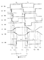
次に、本実施の形態におけるレベルシフト装置の動作を図2のタイミングチャートを用いて説明する。 Next, the operation of the level shift apparatus in this embodiment will be described with reference to the timing chart of FIG.
レベルシフト装置に対する入力信号Sinを図2(a)に示す。この入力信号Sinは、まず相補信号生成回路10のインバータIn1を介してインバータIn2,In3に供給される。さらにインバータIn3を介してインバータIn4に供給される。このとき、インバータIn2の出力信号S1は図2(b)に示すように入力信号Sinに対して所定の遅延τ1をもつ正転信号となり、インバータIn4の出力信号S2は図2(c)に示すように入力信号Sinに対して所定の遅延τ2 をもつ反転信号となる。
An input signal Sin for the level shift device is shown in FIG. This input signal Sin is first supplied to the inverters In2 and In3 via the inverter In1 of the complementary
インバータIn2の出力信号S1は、レベルシフト回路20のNMOSトランジスタQN2のゲートに供給される。図2(b)に示すように時刻t2 においてNMOSトランジスタQN2のゲートにハイレベルの信号が供給されると、NMOSトランジスタQN2はオン状態となる。このとき、インバータIn5からの帰還信号(信号S5の反転信号)はハイレベルであるため、NMOSトランジスタQN1はオン状態となり、PMOSトランジスタQP1はオフ状態となる。また、PMOSトランジスタQP2のゲートは接地されているため、常にオン状態となるが、PMOSトランジスタQP2のオン抵抗はNMOSトランジスタQN2,QN1よりも高抵抗に設定されている。これにより、時刻t2 において、NMOSトランジスタQN2のゲートにハイレベルの信号が供給されると、R-Sラッチ回路LHのNAND回路N1への入力信号S3は、図2(d)に示すようにローレベルとなる。このため、NAND回路N1の出力信号S5は、インバータIn5のゲート容量により、図2(f)の時刻t2より徐々にハイレベルとなる。この出力信号S5は、インバータIn5に供給され、極性を反転してPMOSトランジスタQP1、NMOSトランジスタQN1のゲートに供給される。 The output signal S1 of the inverter In2 is supplied to the gate of the NMOS transistor QN2 of the level shift circuit 20. When a high level signal to the gate of the NMOS transistor QN2 is supplied at time t 2 as shown in FIG. 2 (b), the NMOS transistor QN2 is turned on. At this time, since the feedback signal from the inverter In5 (inversion signal of the signal S5) is at a high level, the NMOS transistor QN1 is turned on and the PMOS transistor QP1 is turned off. Since the gate of the PMOS transistor QP2 is grounded, the PMOS transistor QP2 is always turned on, but the on-resistance of the PMOS transistor QP2 is set to be higher than that of the NMOS transistors QN2 and QN1. Thus, at time t 2, the a high level signal to the gate of the NMOS transistor QN2 is supplied, the input signal S3 to R-S NAND circuit N1 of the latch circuit LH, as shown in FIG. 2 (d) Become low level. Therefore, the output signal S5 of the NAND circuit N1, the gate capacitance of the inverter In5, gradually becomes high-level from the time t 2 in FIG. 2 (f). This output signal S5 is supplied to the inverter In5, inverted in polarity, and supplied to the gates of the PMOS transistor QP1 and the NMOS transistor QN1.
すなわち、R-Sラッチ回路LHのNAND回路N1に入力される入力信号S3の立ち下がりエッジは、所定の遅延の後、PMOSトランジスタQP1、NMOSトランジスタQN1のゲート入力の立ち下がりエッジとして帰還される。この帰還信号により、PMOSトランジスタQP1はオン状態、NMOSトランジスタQN1はオフ状態となり、R-Sラッチ回路LHのNAND回路N1への入力信号S3はハイレベルとなる。このとき、NAND回路N1の他方の入力信号S6はローレベルとなっているため、NAND回路N1の出力信号S5はハイレベルに保持される。 That is, the falling edge of the input signal S3 input to the NAND circuit N1 of the R-S latch circuit LH is fed back as a falling edge of the gate inputs of the PMOS transistor QP1 and the NMOS transistor QN1 after a predetermined delay. By this feedback signal, the PMOS transistor QP1 is turned on, the NMOS transistor QN1 is turned off, and the input signal S3 to the NAND circuit N1 of the RS latch circuit LH becomes high level. At this time, since the other input signal S6 of the NAND circuit N1 is at a low level, the output signal S5 of the NAND circuit N1 is held at a high level.
一方、インバータIn4の出力信号S2は、レベルシフト回路20のNMOSトランジスタQN4のゲートに供給される。図2(c)に示すように時刻t12においてNMOSトランジスタQN4のゲートにハイレベルの信号が供給されると、NMOSトランジスタQN4はオン状態となる。このとき、インバータIn6からの帰還信号(信号S6の反転信号)はハイレベルであるため、NMOSトランジスタQN3はオン状態となり、PMOSトランジスタQP4はオフ状態となる。また、PMOSトランジスタQP4のゲートは接地されているため、常にオン状態となるが、PMOSトランジスタQP4のオン抵抗はNMOSトランジスタQN4,QN3よりも高抵抗に設定されている。これにより、時刻t12において、NMOSトランジスタQN4のゲートにハイレベルの信号が供給されると、R-Sラッチ回路LHのNAND回路N2への入力信号S4は、図2(e)に示すようにローレベルとなる。このため、NAND回路N2の出力信号S6は、インバータIn6のゲート容量により、図2(g)の時刻t12より徐々にハイレベルとなる。この出力信号S6は、インバータIn6に供給され、極性を反転してPMOSトランジスタQP4、NMOSトランジスタQN3のゲートに供給される。 On the other hand, the output signal S2 of the inverter In4 is supplied to the gate of the NMOS transistor QN4 of the level shift circuit 20. When a high level signal to the gate of the NMOS transistor QN4 is supplied at time t 12 as shown in FIG. 2 (c), the NMOS transistor QN4 is turned on. At this time, since the feedback signal from the inverter In6 (inversion signal of the signal S6) is at a high level, the NMOS transistor QN3 is turned on and the PMOS transistor QP4 is turned off. Since the gate of the PMOS transistor QP4 is grounded, the PMOS transistor QP4 is always turned on, but the on-resistance of the PMOS transistor QP4 is set to be higher than that of the NMOS transistors QN4 and QN3. Thus, at time t 12, when a high-level signal to the gate of the NMOS transistor QN4 is supplied, the input signal S4 to the R-S NAND circuit N2 of the latch circuit LH, as shown in FIG. 2 (e) Become low level. Thus, the output signal S6 of NAND circuit N2 is the gate capacitance of the inverter In6, gradually becomes high-level from the time t 12 in FIG. 2 (g). This output signal S6 is supplied to the inverter In6, inverted in polarity, and supplied to the gates of the PMOS transistor QP4 and the NMOS transistor QN3.
すなわち、R-Sラッチ回路LHのNAND回路N2に入力される立ち下がりエッジは、所定の遅延の後、PMOSトランジスタQP4、NMOSトランジスタQN3のゲート入力の立ち下がりエッジとして帰還される。この帰還信号により、PMOSトランジスタQP4はオン状態、NMOSトランジスタQN3はオフ状態となり、R-Sラッチ回路LHのNAND回路N2への入力信号S4はハイレベルとなる。このとき、NAND回路N2の他方の入力信号S5はローレベルとなっているため、NAND回路N2の出力信号S6はハイレベルに保持される。 That is, the falling edge input to the NAND circuit N2 of the RS latch circuit LH is fed back as a falling edge of the gate inputs of the PMOS transistor QP4 and the NMOS transistor QN3 after a predetermined delay. By this feedback signal, the PMOS transistor QP4 is turned on, the NMOS transistor QN3 is turned off, and the input signal S4 to the NAND circuit N2 of the RS latch circuit LH becomes high level. At this time, since the other input signal S5 of the NAND circuit N2 is at a low level, the output signal S6 of the NAND circuit N2 is held at a high level.
したがって、NMOSトランジスタQN2,QN4のゲートにハイレベルの信号が供給されると、所定の遅延の後、NAND回路N1,N2の出力信号S5,S6はハイレベルとなる。NAND回路N1,N2は互いの出力を他方の入力に帰還する接続であるため、時刻t3 においてNAND回路N1の出力信号S5がハイレベルになると、NAND回路N2の出力信号S6は、図2(g)のようにインバータIn6のゲート容量により徐々にローレベルになる。また、時刻t13においてNAND回路N2の出力信号S6がハイレベルになると、NAND回路N1の出力信号S5は、図2(f)のように、インバータIn5のゲート容量により徐々にローレベルになる。 Therefore, when a high level signal is supplied to the gates of the NMOS transistors QN2 and QN4, the output signals S5 and S6 of the NAND circuits N1 and N2 become high level after a predetermined delay. Since NAND circuits N1, N2 is connected to the feedback output of each other to the other input, the output signal S5 of the NAND circuit N1 becomes high level at time t 3, the output signal S6 of the NAND circuit N2 is 2 ( As shown in g), the level gradually becomes low due to the gate capacitance of the inverter In6. When the output signal S6 of the NAND circuit N2 becomes high level at time t 13, the output signal S5 of the NAND circuit N1, as shown in FIG. 2 (f), the level gradually due to the gate capacitance of the inverter In5.
NAND回路N1,N2の出力信号S5,S6は、それぞれインバータIn7,In8に供給され、図2(h),(i)のように極性が反転され、デューティ補正回路30の第1、第2の入力に供給される。ここで、第1、第2の入力信号S7,S8は、同時にハイレベルになることはない。インバータIn7の出力信号S7の立ち上がりエッジは、インバータIn8の出力信号S8の立ち下がりエッジよりも時間的に後方に位置することになる。 The output signals S5 and S6 of the NAND circuits N1 and N2 are respectively supplied to the inverters In7 and In8, and their polarities are inverted as shown in FIGS. 2 (h) and 2 (i). Supplied to the input. Here, the first and second input signals S7 and S8 do not become high level at the same time. The rising edge of the output signal S7 of the inverter In7 is located behind the falling edge of the output signal S8 of the inverter In8.
デューティ補正回路30の第1の入力信号S7はNMOSトランジスタQN5のゲートに供給され、第2の入力信号S8はNMOSトランジスタQN6のゲートに供給される。すなわち、インバータIn10の入力信号S9は、図2(j)の時刻t14において、第1の入力信号S7の立ち上がりエッジに同期して、ローレベルに変化する。続いて、所定の遅延τ3 ののち、インバータIn10の出力信号S10がハイレベルに変化する。また、インバータIn9の入力信号S10は、図2(k)の時刻t4 において、第2の入力信号S8の立ち上がりエッジに同期して、ローレベルに変化する。続いて、所定の遅延τ4 ののち、インバータIn9の出力であるレベルシフト出力信号S9がハイレベルに変化する。
The first input signal S7 of the
したがって、時刻t1 〜t21の1周期の入力信号Sinにおいて、出力バッファB1のレベルシフト出力信号S9は、時刻t5〜t14の期間においてハイレベルとなり、時刻t1 〜時刻t5 の期間、および、時刻t14〜時刻t21の期間においてローレベルとなる。 Accordingly, the input signal Sin of one period of time t 1 ~t 21, level shift output signal S9 of the output buffer B1 is a high level in the period of time t 5 ~t 14, the period of time t 1 ~ time t 5 , And during the period from time t 14 to time t 21 .
レベルシフト回路20は入力となる相補信号に対して対称な回路構成とすることで、NAND回路N1の入力信号S3の立ち下がりエッジからインバータIn8の出力信号S8の立ち上がりエッジまでの遅延τP と、NAND回路N2の入力信号S4の立ち下がりエッジからインバータIn7の出力信号S7の立ち上がりエッジまでの遅延τQ の長さが等しくなるようにしている(この点は従来の技術でも同じ)。 The level shift circuit 20 has a symmetric circuit configuration with respect to the complementary signal as an input, so that the delay τ P from the falling edge of the input signal S3 of the NAND circuit N1 to the rising edge of the output signal S8 of the inverter In8, The lengths of the delays τ Q from the falling edge of the input signal S4 of the NAND circuit N2 to the rising edge of the output signal S7 of the inverter In7 are made equal (this is also the case with the prior art).
そのうえで、デューティ補正回路30において、NMOSトランジスタQN5をインバータIn7の出力信号S7で制御することにより、インバータIn8の出力信号S8の立ち下がりエッジをインバータIn7の出力信号S7の立ち上がりエッジのタイミングまで後方にτT (=τQ −τR =τR )ずらしてレベルシフト出力信号S9の立ち下がりエッジとしている。また、インバータIn9とインバータIn10の逆並列接続により、インバータIn8の出力信号S8に対してレベルシフト出力信号S9の立ち上がりエッジをτ4 だけ遅延させている。このτT とτ4 のずらしにより、相補信号生成回路10におけるτ2 とτ1 の遅延差を相殺し、入力信号のデューティ比に対する出力信号のデューティ比の誤差を軽減している。以下に具体的に説明する。
Then, in the
ここで、レベルシフト出力信号S9のハイレベル期間をTH ′とし、ローレベル期間をTL ′とする。 Here, the high level period of the level shift output signal S9 is T H ′, and the low level period is T L ′.
TH ′=TH−τ4 +τT
TL ′=TL−τT +τ4
ローレベル期間TL ′とハイレベル期間TH ′との差分ΔT′は、
ΔT′=TL ′−TH ′
であるが、本実施の形態のこの差分ΔT′が従来の技術の場合の差分ΔT=TL −TH とどれほどちがうかを計算する。すなわち、δ=ΔT′−ΔTを計算する。
T H ′ = T H −τ 4 + τ T
T L ′ = T L −τ T + τ 4
The difference ΔT ′ between the low level period T L ′ and the high level period T H ′ is
ΔT ′ = T L ′ −T H ′
Although, the difference [Delta] T 'of the present embodiment can calculate how much different the difference ΔT = T L -T H in the prior art. That is, δ = ΔT′−ΔT is calculated.
δ=ΔT′−ΔT
=TL ′−TH ′−ΔT
=(TL −τT +τ4 )−(TH −τ4 +τT )−ΔT
=(TL −TH )−ΔT−τT +τ4 +τ4 −τT
=2(τ4 −τT)
ここで、τ4 <τT であるので、結局、
δ<0
となる。
δ = ΔT′−ΔT
= T L '-T H ' -ΔT
= (T L −τ T + τ 4 ) − (T H −τ 4 + τ T ) −ΔT
= (T L -T H ) -ΔT-τ T + τ 4 + τ 4 -τ T
= 2 (τ 4 −τ T )
Here, since τ 4 <τ T ,
δ <0
It becomes.
端的には、図2(i)の信号S8のハイレベル期間TH を図2(j)のレベルシフト出力信号S9のハイレベル期間TH ′へ変化させるのに、立ち上がりエッジを時間の正方向に沿ってτ4だけシフトさせ、立ち下がりエッジを同じく時間の正方向に沿ってτT だけシフトさせているので、差し引き、(τT −τ4 )だけ時間幅を伸ばしていることになる((τT −τ4 )はプラス)。つまり、従来の技術でローレベル期間TL より短かったハイレベル期間TH を伸ばすことにより、ローレベル期間TL ′とハイレベル期間TH ′との差分ΔT′をより小さいものに修正している。すなわち、本実施の形態の場合のローレベル期間TL ′とハイレベル期間TH ′との差分ΔT′は、従来の技術の場合の差分ΔTよりも小さいものになっている。これがδ<0ということである。 Briefly, to alter the high-level period T H of the signal S8 in FIG. 2 (i) to FIG. 2 (j) level high-level period of the shift output signal S9 T H 'and the positive direction of the rising edge time shifted by tau 4 along, since only by shifting falling along the positive direction of the same time the edge tau T, subtracted, it means that extending the duration only (τ T -τ 4) ( (Τ T −τ 4 ) is positive). That is, the difference ΔT ′ between the low level period T L ′ and the high level period T H ′ is corrected to be smaller by extending the high level period T H that is shorter than the low level period T L in the conventional technique. Yes. That is, the difference ΔT ′ between the low level period T L ′ and the high level period T H ′ in the present embodiment is smaller than the difference ΔT in the conventional technique. This is δ <0.
デューティ補正回路30は、レベルシフト回路20のR-Sラッチ回路LHにおけるNAND回路N1の出力信号S5をインバータIn7によって反転して矩形波信号S7を作り、この矩形波信号S7を利用してレベルシフト回路20の出力信号S8のデューティ比を補正するものである。
The
レベルシフト回路20の出力信号S8の立ち下がりエッジを矩形波信号S7の立ち上がりエッジまで遅らせて、レベルシフト出力信号S9の立ち下がりエッジを規定している。この遅延時間τT =(τQ −τR )=τR は、矩形波信号S7の元のNAND回路N1の出力信号S5が徐々に減少することから比較的に長いものになっている。 The falling edge of the output signal S8 of the level shift circuit 20 is delayed until the rising edge of the rectangular wave signal S7, thereby defining the falling edge of the level shift output signal S9. This delay time τ T = (τ Q −τ R ) = τ R is relatively long because the output signal S5 of the original NAND circuit N1 of the rectangular wave signal S7 gradually decreases.
一方、レベルシフト回路20の出力信号S8の立ち上がりエッジをインバータIn9,In10の逆並列接続でτ4 だけ遅延させて、レベルシフト出力信号S9の立ち上がりエッジを規定している。この遅延時間τ4 は、遅延時間τT よりも短い。 On the other hand, the rising edge of the output signal S8 of the level shift circuit 20 is delayed by τ 4 by the inverse parallel connection of the inverters In9 and In10 to define the rising edge of the level shift output signal S9. This delay time τ 4 is shorter than the delay time τ T.
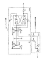
(実施の形態2)
図3は本発明の実施の形態2におけるレベルシフト装置の構成を示す回路図である。
(Embodiment 2)
FIG. 3 is a circuit diagram showing a configuration of a level shift apparatus according to
レベルシフト回路20の2本の出力信号をそれぞれ第1、第2の入力信号S7,S8とし、第1の入力信号S7がインバータIn11を介してゲートに接続され、ソースが高電位電源に接続される第1のPMOSトランジスタQP5と、第2の入力信号S8がインバータIn12を介してゲートに接続され、ソースが高電位電源に接続される第2のPMOSトランジスタQP6と、入力端子が第2のPMOSトランジスタQP6のドレインに接続され、出力端子が第1のPMOSトランジスタQP5のドレインに接続される第1のインバータIn9と、入力端子が第1のPMOSトランジスタQP5のドレインに接続され、出力端子が第2のPMOSトランジスタQP6のドレインに接続される第2のインバータIn10と、第1のインバータIn9の出力信号を入力信号とする第3のインバータIn13と、第2のインバータIn10の出力信号を入力信号とする第4のインバータIn14から構成されている。 The two output signals of the level shift circuit 20 are first and second input signals S7 and S8, respectively. The first input signal S7 is connected to the gate via the inverter In11, and the source is connected to the high potential power source. The first PMOS transistor QP5, the second input signal S8 is connected to the gate via the inverter In12, the source is connected to the high potential power source, and the input terminal is the second PMOS. The first inverter In9 is connected to the drain of the transistor QP6, the output terminal is connected to the drain of the first PMOS transistor QP5, the input terminal is connected to the drain of the first PMOS transistor QP5, and the output terminal is the second. A second inverter In10 connected to the drain of the PMOS transistor QP6, and a first inverter A third inverter In13 to the input signal an output signal of In9, and a fourth inverter In14 to the input signal an output signal of the second inverter In10.
本実施の形態のレベルシフト装置の動作は、実施の形態1の場合と同様である。 The operation of the level shift apparatus of the present embodiment is the same as that of the first embodiment.
本発明の技術は、デューティ比を変化させずにレベルシフトを行うレベルシフト装置として有用である。 The technology of the present invention is useful as a level shift device that performs level shift without changing the duty ratio.
10 相補信号生成回路
20 レベルシフト回路
30 デューティ補正回路
B1 第1のバッファ
B2 第2のバッファ
In1〜In8,In11〜In14 インバータ
In9 第1のインバータ
In10 第2のインバータ
LH R-Sラッチ回路
N1,N2 NAND回路
QN1〜QN4 NMOSトランジスタ
QN5 第1のNMOSトランジスタ
QN6 第2のNMOSトランジスタ
QP1〜QP4 PMOSトランジスタ
QP5 第1のPMOSトランジスタ
QP6 第2のPMOSトランジスタ
DESCRIPTION OF
Claims (4)
前記レベルシフト回路の出力信号を入力して、前記入力信号のデューティに対する前記レベルシフト回路の出力信号のデューティのずれを相殺するデューティ補正回路とを備えたレベルシフト装置。 A level shift circuit that performs voltage level conversion on one input signal and outputs a signal after voltage level conversion;
A level shift apparatus comprising: a duty correction circuit that receives an output signal of the level shift circuit and cancels a deviation of the duty of the output signal of the level shift circuit with respect to the duty of the input signal.
前記レベルシフト回路における前記R-Sラッチ回路からの2本の出力信号をそれぞれ第1、第2の入力信号とし、前記第1の入力信号がゲートに接続され、ソースが接地される第1のNMOSトランジスタと、前記第2の入力信号がゲートに接続され、ソースが接地される第2のNMOSトランジスタと、入力端子が前記第2のNMOSトランジスタのドレインに接続され、出力端子が前記第1のNMOSトランジスタのドレインに接続される第1のインバータと、入力端子が前記第1のNMOSトランジスタのドレインに接続され、出力端子が前記第2のNMOSトランジスタのドレインに接続される第2のインバータと、前記第1のインバータの出力信号を入力信号としレベルシフトの出力とする第1のバッファと、前記第2のインバータの出力信号を入力信号とする第2のバッファからなるデューティ補正回路とを備えたレベルシフト装置。 A level shift circuit that performs voltage level conversion on one input signal and outputs the signal after voltage level conversion as two signals by an RS latch circuit;
Two output signals from the RS latch circuit in the level shift circuit are first and second input signals, respectively, the first input signal is connected to the gate, and the source is grounded. An NMOS transistor, a second NMOS transistor having the second input signal connected to the gate and a source grounded, an input terminal connected to the drain of the second NMOS transistor, and an output terminal connected to the first NMOS A first inverter connected to the drain of the NMOS transistor; a second inverter having an input terminal connected to the drain of the first NMOS transistor and an output terminal connected to the drain of the second NMOS transistor; A first buffer that uses an output signal of the first inverter as an input signal and outputs a level shift; and the second inverter And a duty correction circuit composed of a second buffer using the output signal of the data as an input signal.
前記レベルシフト回路における前記R-Sラッチ回路からの2本の出力信号をそれぞれ第1、第2の入力信号とし、前記第1の入力信号がゲートに接続され、ソースが高電位電源に接続される第1のPMOSトランジスタと、前記第2の入力信号がゲートに接続され、ソースが高電位電源に接続される第2のPMOSトランジスタと、入力端子が前記第2のPMOSトランジスタのドレインに接続され、出力端子が前記第1のPMOSトランジスタのドレインに接続される第1のインバータと、入力端子が前記第1のPMOSトランジスタのドレインに接続され、出力端子が前記第2のPMOSトランジスタのドレインに接続される第2のインバータと、前記第1のインバータの出力信号を入力信号としレベルシフトの出力とする第1のバッファと、前記第2のインバータの出力信号を入力信号とする第2のバッファからなるデューティ補正回路とを備えたレベルシフト装置。 A level shift circuit that performs voltage level conversion on one input signal and outputs the signal after voltage level conversion as two signals by an RS latch circuit;
The two output signals from the RS latch circuit in the level shift circuit are first and second input signals, respectively, the first input signal is connected to the gate, and the source is connected to the high potential power source. The first PMOS transistor, the second input signal is connected to the gate, the second PMOS transistor is connected to the high potential power source, and the input terminal is connected to the drain of the second PMOS transistor. A first inverter whose output terminal is connected to the drain of the first PMOS transistor; an input terminal connected to the drain of the first PMOS transistor; and an output terminal connected to the drain of the second PMOS transistor. And a first buffer that uses the output signal of the first inverter as an input signal and a level shift output. And a duty correction circuit comprising a second buffer having the output signal of the second inverter as an input signal.
Priority Applications (2)
| Application Number | Priority Date | Filing Date | Title |
|---|---|---|---|
| JP2006238832A JP2008061176A (en) | 2006-09-04 | 2006-09-04 | Level shifter apparatus |
| US11/896,528 US7667520B2 (en) | 2006-09-04 | 2007-09-04 | Level shift device having reduced error in the duty ratio of the output signal |
Applications Claiming Priority (1)
| Application Number | Priority Date | Filing Date | Title |
|---|---|---|---|
| JP2006238832A JP2008061176A (en) | 2006-09-04 | 2006-09-04 | Level shifter apparatus |
Publications (2)
| Publication Number | Publication Date |
|---|---|
| JP2008061176A true JP2008061176A (en) | 2008-03-13 |
| JP2008061176A5 JP2008061176A5 (en) | 2009-09-10 |
Family
ID=39243372
Family Applications (1)
| Application Number | Title | Priority Date | Filing Date |
|---|---|---|---|
| JP2006238832A Withdrawn JP2008061176A (en) | 2006-09-04 | 2006-09-04 | Level shifter apparatus |
Country Status (2)
| Country | Link |
|---|---|
| US (1) | US7667520B2 (en) |
| JP (1) | JP2008061176A (en) |
Cited By (1)
| Publication number | Priority date | Publication date | Assignee | Title |
|---|---|---|---|---|
| WO2009113240A1 (en) | 2008-03-11 | 2009-09-17 | パナソニック株式会社 | Film electrode assembly |
Families Citing this family (1)
| Publication number | Priority date | Publication date | Assignee | Title |
|---|---|---|---|---|
| JP5074223B2 (en) * | 2008-02-06 | 2012-11-14 | ルネサスエレクトロニクス株式会社 | Level shift circuit and driver and display device using the same |
Family Cites Families (7)
| Publication number | Priority date | Publication date | Assignee | Title |
|---|---|---|---|---|
| US5912574A (en) * | 1996-12-09 | 1999-06-15 | Sun Microsystems, Inc. | Dual loop PLL with secondary loop to achieve 50% duty cycle |
| JP3123952B2 (en) * | 1997-09-30 | 2001-01-15 | 日本電気アイシーマイコンシステム株式会社 | Output buffer circuit |
| JP4327411B2 (en) * | 2001-08-31 | 2009-09-09 | 株式会社ルネサステクノロジ | Semiconductor device |
| US6933755B2 (en) * | 2002-11-04 | 2005-08-23 | Lg Electronics Inc. | Output driving circuit for maintaining I/O signal duty ratios |
| US20050134355A1 (en) * | 2003-12-18 | 2005-06-23 | Masato Maede | Level shift circuit |
| JP4502767B2 (en) * | 2004-09-29 | 2010-07-14 | 株式会社リコー | Level shift circuit |
| US7355446B2 (en) * | 2005-05-20 | 2008-04-08 | Samsung Electronics Co., Ltd. | Voltage conversion circuit with stable transition delay characteristic |
-
2006
- 2006-09-04 JP JP2006238832A patent/JP2008061176A/en not_active Withdrawn
-
2007
- 2007-09-04 US US11/896,528 patent/US7667520B2/en not_active Expired - Fee Related
Cited By (1)
| Publication number | Priority date | Publication date | Assignee | Title |
|---|---|---|---|---|
| WO2009113240A1 (en) | 2008-03-11 | 2009-09-17 | パナソニック株式会社 | Film electrode assembly |
Also Published As
| Publication number | Publication date |
|---|---|
| US7667520B2 (en) | 2010-02-23 |
| US20080246528A1 (en) | 2008-10-09 |
Similar Documents
| Publication | Publication Date | Title |
|---|---|---|
| JP4502767B2 (en) | Level shift circuit | |
| KR101120047B1 (en) | Single signal-to-differential signal converter and conversion method | |
| US8384438B1 (en) | Single-to-differential conversion circuit and method | |
| US7468621B2 (en) | Synchronization circuits and methods | |
| JP3596969B2 (en) | Delay circuit and pulse generation circuit | |
| JP2012023533A5 (en) | ||
| JP2008061176A (en) | Level shifter apparatus | |
| TWI401890B (en) | Voltage level converter | |
| US20150381154A1 (en) | Flip-flop circuit | |
| JP2007258891A (en) | Complementary signal generating circuit | |
| TW201817166A (en) | Selectable delay buffer | |
| US9257977B1 (en) | Duty-cycle distortion self-correcting delay line | |
| JP4340195B2 (en) | Signal generation circuit and level shifter with signal generation circuit | |
| US8487682B2 (en) | Multi-phase clock generator | |
| EP2399340B1 (en) | Pulse-shrinking delay line based on feed forward | |
| WO2012165599A1 (en) | Level shift circuit | |
| KR20220085266A (en) | Power domain changing circuit and operation method thereof | |
| US20140049308A1 (en) | Level shift circuit | |
| JP2007096452A (en) | Level shift circuit | |
| JP2012105135A (en) | Differential output circuit | |
| US8547139B2 (en) | CMOS logic integrated circuit | |
| CN107404316B (en) | Signal multiplexing device | |
| US8344782B2 (en) | Method and apparatus to limit circuit delay dependence on voltage for single phase transition | |
| KR100924354B1 (en) | Input buffer | |
| JP2014230134A (en) | Delay adjustment circuit |
Legal Events
| Date | Code | Title | Description |
|---|---|---|---|
| A521 | Written amendment |
Free format text: JAPANESE INTERMEDIATE CODE: A523 Effective date: 20090722 |
|
| A621 | Written request for application examination |
Free format text: JAPANESE INTERMEDIATE CODE: A621 Effective date: 20090722 |
|
| A761 | Written withdrawal of application |
Free format text: JAPANESE INTERMEDIATE CODE: A761 Effective date: 20110908 |
|
| A977 | Report on retrieval |
Free format text: JAPANESE INTERMEDIATE CODE: A971007 Effective date: 20110920 |