JP2008046292A - Manufacturing method of information display panel - Google Patents
Manufacturing method of information display panel Download PDFInfo
- Publication number
- JP2008046292A JP2008046292A JP2006220925A JP2006220925A JP2008046292A JP 2008046292 A JP2008046292 A JP 2008046292A JP 2006220925 A JP2006220925 A JP 2006220925A JP 2006220925 A JP2006220925 A JP 2006220925A JP 2008046292 A JP2008046292 A JP 2008046292A
- Authority
- JP
- Japan
- Prior art keywords
- display panel
- information display
- short
- display medium
- electrodes
- Prior art date
- Legal status (The legal status is an assumption and is not a legal conclusion. Google has not performed a legal analysis and makes no representation as to the accuracy of the status listed.)
- Pending
Links
Images


Landscapes
- Liquid Crystal (AREA)
- Devices For Indicating Variable Information By Combining Individual Elements (AREA)
Abstract
Description
本発明は、少なくとも一方が透明な2枚の基板間に形成した気中空間に、光学的反射率および帯電性を有する表示媒体を封入し、基板に設けた対電極間に所定電圧を印加することにより発生させた電界を表示媒体に付与することによって、表示媒体を移動させて画像等の情報を表示する情報表示用パネルの製造方法に関するものである。 According to the present invention, a display medium having optical reflectivity and chargeability is sealed between air cavities formed between two substrates, at least one of which is transparent, and a predetermined voltage is applied between counter electrodes provided on the substrate. The present invention relates to a method for manufacturing an information display panel that displays information such as an image by moving the display medium by applying an electric field generated thereby.
情報表示装置の従来例としては、液晶表示装置(LCD)がある。液晶表示装置を構成する液晶パネルは、対向配置した2枚のITO電極付きガラス基板間に液晶を封入する構造となっている。このような液晶パネルの製造工程において、ガラス基板上に形成したITO電極パターンにショート不良部位が発見された場合、レーザー式リペア装置を用いてガラス基板上のITO電極パターンのショート不良部位を除去する補修技術が知られている。 As a conventional example of the information display device, there is a liquid crystal display device (LCD). The liquid crystal panel constituting the liquid crystal display device has a structure in which liquid crystal is sealed between two glass substrates with ITO electrodes arranged opposite to each other. In such a liquid crystal panel manufacturing process, when a short-circuit defective portion is found in the ITO electrode pattern formed on the glass substrate, the short-circuit defective portion of the ITO electrode pattern on the glass substrate is removed using a laser type repair device. Repair technology is known.
組立が完了した液晶パネル(完成した液晶パネル)は、ガラス基板間に液晶が封入済みであるため、ガラス基板上に形成したITO電極パターンにショート不良部位があったとしても、そのショート不良部位を補修することができない。したがって、上記レーザー式リペア装置を用いてITO電極パターンのショート不良部位を除去する補修技術は、液晶パネルとしての組立が完了する前の状態、すなわち液晶の封入も基板の貼り合わせも行われていない状態である「ITO電極付きガラス基板の状態」にしか適用することができない。そのため、ITO電極付きガラス基板の状態で、言い換えれば製品完成前のパーツ状態で、本来の製造工程とは異なるレーザーリペア工程にITO電極付きガラス基板を移動させてITO電極パターンのショート不良部位を発見し、そのショート不良部位をレーザー式リペア装置で除去した後に、製造工程に戻して後続の工程を実行しなければならないため、生産効率が悪くなる。 Since the liquid crystal panel (completed liquid crystal panel) that has been assembled has liquid crystal sealed between the glass substrates, even if there is a short-circuit defective portion on the ITO electrode pattern formed on the glass substrate, It cannot be repaired. Therefore, the repair technique for removing the short-circuit defective portion of the ITO electrode pattern using the laser type repair device is in a state before the assembly as the liquid crystal panel is completed, that is, the liquid crystal is not sealed and the substrate is not bonded. It can be applied only to the “state of glass substrate with ITO electrode” which is in the state. Therefore, in the state of the glass substrate with ITO electrodes, in other words, in the part state before the product is completed, the glass substrate with ITO electrodes is moved to a laser repair process that is different from the original manufacturing process, and the short-circuit defective part of the ITO electrode pattern is found. In addition, after removing the short-circuit defective portion with the laser type repair device, it is necessary to return to the manufacturing process and execute the subsequent process, resulting in poor production efficiency.
本発明は、完成した乾式の情報表示用パネルの電極間ショートや電極配線間ショートを除去するショート除去工程を行うことにより、生産効率の良い情報表示用パネルの製造方法を提供することを目的とする。 It is an object of the present invention to provide a method for manufacturing an information display panel with high production efficiency by performing a short removing process for removing a short circuit between electrodes and a short circuit between electrode wirings of a completed dry information display panel. To do.
上記目的を達成するため、本発明の情報表示用パネルの製造方法は、少なくとも一方が透明な2枚の基板間に形成した気中空間に、光学的反射率および帯電性を有する表示媒体を封入し、基板に設けた対電極間に所定電圧を印加することにより発生させた電界を表示媒体に付与することによって、表示媒体を移動させて画像等の情報を表示する情報表示用パネルの製造方法であって、完成した情報表示用パネルに電極間ショートや電極配線間ショートがあるか否かを検査する検査工程と、完成した情報表示用パネルに電極間ショートや電極配線間ショートがあった場合に、電極間ショートや電極配線間ショートを有する基板の外側に配置したレーザー式リペア装置から電極間ショートや電極配線間ショートを有する部位に、所定発振波長、所定最大エネルギー、所定最大ピークパワーおよび所定パルス幅を有するレーザー光線を照射することにより、当該電極間ショートや当該電極配線間ショートを除去するショート除去工程と、を行うことを特徴とする。 In order to achieve the above object, a method for manufacturing an information display panel according to the present invention encloses a display medium having optical reflectivity and chargeability between air cavities formed between two substrates, at least one of which is transparent. And an information display panel for displaying information such as an image by moving the display medium by applying an electric field generated by applying a predetermined voltage between the counter electrodes provided on the substrate to the display medium. When the completed information display panel has an inspection process to check whether there is a short between electrodes or electrode wiring, and when the completed information display panel has a short between electrodes or short between electrodes In addition, from a laser type repair device arranged outside the substrate having a short between electrodes or a short between electrode wires, a portion having a short between electrodes or a short between electrode wires may have a predetermined oscillation wavelength, Maximum energy, by irradiating a laser beam having a predetermined maximum peak power and a predetermined pulse width, and carrying out a short removal step of removing the short circuit between electrodes and the electrodes short circuit between wires, a.
本発明の情報表示用パネルの製造方法の好適例としては、前記レーザー式リペア装置のレーザーはYAGレーザーであり、前記所定発振波長は266〜1064nmであり、前記最大エネルギーは1〜12mJ/pulseであり、前記最大ピークパワーは0.2〜2MWであり、前記パルス幅は5〜8nsecであること、および、前記表示媒体が白色表示媒体、黒色表示媒体、または白色表示媒体と黒色表示媒体との組合せであること、がある。 As a preferred example of the method for producing the information display panel of the present invention, the laser of the laser type repair device is a YAG laser, the predetermined oscillation wavelength is 266 to 1064 nm, and the maximum energy is 1 to 12 mJ / pulse. The maximum peak power is 0.2 to 2 MW, the pulse width is 5 to 8 nsec, and the display medium is a white display medium, a black display medium, or a white display medium and a black display medium. Be a combination.
上記本発明の情報表示用パネルの製造方法によれば、作製する情報表示用パネルが、少なくとも一方が透明な2枚の基板間に形成した気中空間に、光学的反射率および帯電性を有する表示媒体を封入し、基板に設けた対電極間に所定電圧を印加することにより発生させた電界を表示媒体に付与することによって、表示媒体を移動させて画像等の情報を表示する情報表示用パネル、言い換えれば内部に空気等の気体が存在する乾式の情報表示用パネルであるため、完成した情報表示用パネルの基板上に形成した電極や配線パターンに電極間ショートや電極配線間ショートがあった場合には、例えば製造工程の最後尾に設けた検査工程でその電極間ショートを発見して補修することができる。したがって、完成した情報表示用パネルに電極間ショートや電極配線間ショートがあった場合には、ショート除去工程で、電極間ショートや電極配線間ショートを有する基板の外側に配置したレーザー式リペア装置から電極間ショートや電極配線間ショートを有する部位に、所定発振波長、所定最大エネルギー、所定最大ピークパワーおよび所定パルス幅を有するレーザー光線を照射することにより、当該電極間ショートや当該電極配線間ショートが除去されるので、生産効率の良い情報表示用パネルの製造方法を提供することができる。 According to the method for manufacturing an information display panel of the present invention, the information display panel to be produced has optical reflectivity and chargeability between the air and hollow formed between two substrates, at least one of which is transparent. For information display that displays information such as images by moving the display medium by applying an electric field generated by encapsulating the display medium and applying a predetermined voltage between the counter electrodes provided on the substrate to the display medium Since the panel is a dry information display panel in which a gas such as air exists, in other words, there is a short circuit between electrodes or a short circuit between electrode wirings on the electrode or wiring pattern formed on the substrate of the completed information display panel. In this case, for example, it is possible to find and repair the short-circuit between the electrodes in an inspection process provided at the end of the manufacturing process. Therefore, if there is a short between electrodes or a short between electrode wires in the completed information display panel, in the short removal process, from the laser type repair device placed outside the substrate having the short between electrodes or short between electrode wires By irradiating a laser beam having a predetermined oscillation wavelength, a predetermined maximum energy, a predetermined maximum peak power, and a predetermined pulse width to a part having an inter-electrode short or an inter-electrode short, the inter-electrode short or the inter-electrode short is removed. Therefore, a method for manufacturing an information display panel with high production efficiency can be provided.
以下、本発明を実施するための最良の形態を図面に基づき詳細に説明する。 Hereinafter, the best mode for carrying out the present invention will be described in detail with reference to the drawings.
まず、本発明の製造方法によって作製する情報表示用パネルの構成について説明する。本発明の製造方法によって作製する情報表示用パネルでは、対向する2枚の基板間に封入した表示媒体に電界が付与される。付与された電界方向に沿って、表示媒体が電界による力やクーロン力などによって引き寄せられ、表示媒体が電界方向の変化によって移動方向を変えることにより、画像等の情報表示がなされる。従って、表示媒体が、均一に移動し、かつ、繰り返し表示情報を書き換える時あるいは表示情報を継続して表示する時の安定性を維持できるように、情報表示用パネルを設計する必要がある。ここで、表示媒体を構成する粒子にかかる力は、粒子同士のクーロン力により引き付けあう力の他に、電極や基板との電気鏡像力、分子間力、液架橋力、重力などが考えられる。 First, the structure of the information display panel manufactured by the manufacturing method of the present invention will be described. In the information display panel manufactured by the manufacturing method of the present invention, an electric field is applied to a display medium sealed between two opposing substrates. Along with the applied electric field direction, the display medium is attracted by the force of the electric field, the Coulomb force, or the like, and the display medium changes the moving direction by the change of the electric field direction, thereby displaying information such as an image. Therefore, it is necessary to design the information display panel so that the display medium can move uniformly and maintain the stability when the display information is rewritten or when the display information is continuously displayed. Here, as the force applied to the particles constituting the display medium, in addition to the force attracting each other by the Coulomb force between the particles, an electric mirror image force between the electrode and the substrate, an intermolecular force, a liquid cross-linking force, gravity and the like can be considered.
本発明の製造方法によって作製する情報表示用パネルの例を、図1(a),(b)〜図3(a),(b)に基づき説明する。 An example of an information display panel manufactured by the manufacturing method of the present invention will be described with reference to FIGS. 1 (a) and 1 (b) to FIGS. 3 (a) and 3 (b).
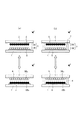
図1(a),(b)に示す例では、少なくとも1種以上の粒子から構成される光学的反射率および帯電特性の異なる少なくとも2種以上の表示媒体3(ここでは白色表示媒体用粒子3Waの粒子群からなる白色表示媒体3Wと黒色表示媒体用粒子3Baの粒子群からなる黒色表示媒体3Bを示す)を、基板1に設けたライン電極5と基板2に設けたライン電極6との間に電圧を印加することにより発生する電界に応じて、基板1、2と垂直に移動させ、黒色表示媒体3Bを観察者に視認させて黒色の表示を行うか、あるいは、白色表示媒体3Wを観察者に視認させて白色の表示を行っている。なお、図1(b)に示す例では、図1(a)に示す例に加えて、基板1、2の間に例えば格子状に隔壁4を設けセルを形成している。また、図1(b)において、手前にある隔壁は省略している。
In the example shown in FIGS. 1A and 1B, at least two kinds of display media 3 (here, white display medium particles 3Wa) having at least one kind of particles and having different optical reflectance and charging characteristics. Between the
図2(a),(b)に示す例では、少なくとも1種以上の粒子から構成される光学的反射率および帯電特性の異なる少なくとも2種以上の表示媒体3(ここでは白色表示媒体用粒子3Waの粒子群からなる白色表示媒体3Wと黒色表示媒体用粒子3Baの粒子群からなる黒色表示媒体3Bを示す)を、基板1に設けた個別電極5と基板2に設けた個別電極6との間に電圧を印加することにより発生する電界に応じて、基板1、2と垂直に移動させ、黒色表示媒体3Bを観察者に視認させて黒色の表示を行うか、あるいは、白色表示媒体3Wを観察者に視認させて白色の表示を行っている。なお、図2(b)に示す例では、図1(a)に示す例に加えて、基板1、2の間に例えば格子状に隔壁4を設けセルを形成している。また、図2(b)において、手前にある隔壁は省略している。
In the example shown in FIGS. 2A and 2B, at least two kinds of display media 3 (here, white display medium particles 3Wa) having at least one kind of particles and having different optical reflectance and charging characteristics. Between the
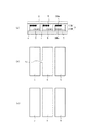
図3(a),(b)に示す例では、少なくとも1種以上の粒子から構成される光学的反射率および帯電性を有する1種の表示媒体3(ここでは白色表示媒体用粒子3Waの粒子群からなる白色表示媒体3Wを示す)を、基板1に設けた電極5と基板2に設けた電極6との間に電圧を印加することにより発生する電界に応じて、基板1、2と平行方向に移動させ、白色表示媒体3Wを観察者に視認させて白色の表示を行うか、あるいは、電極6または基板1の色を観察者に視認させて電極6または基板1の色の表示を行っている。なお、図3(b)に示す例では、図3(a)に示す例に加えて、基板1、2の間に例えば格子状の隔壁4を設けセルを形成している。また、図3(b)において、手前にある隔壁は省略している。
電極は、基板の外側に設けても、基板の内側に設けても、基板内部に埋め込むように設けてもよい。
In the example shown in FIGS. 3A and 3B, one type of display medium 3 (here, particles of white display medium particles 3Wa) having optical reflectivity and chargeability composed of at least one type of particles. A
The electrode may be provided outside the substrate, inside the substrate, or embedded in the substrate.
以上の説明は、粒子群からなる白色表示媒体3Wを粉流体からなる白色表示媒体に、粒子群からなる黒色表示媒体3Bを粉流体からなる黒色表示媒体に、それぞれ置き換えた場合も同様に適用することができる。粉流体については後述する。
The above description is similarly applied to the case where the
以下、本発明の情報表示用パネルの製造方法を詳細に説明する。本発明の情報表示用パネルの製造方法は、少なくとも一方が透明な2枚の基板間に形成した気中空間に、光学的反射率および帯電性を有する表示媒体を封入し、基板に設けた対電極間に所定電圧を印加することにより発生させた電界を表示媒体に付与することによって、表示媒体を移動させて画像等の情報を表示する情報表示用パネルを作製するものであり、完成した情報表示用パネルに電極間ショートや電極配線間ショートがあるか否かを検査する検査工程と、完成した情報表示用パネルに電極間ショートや電極配線間ショートがあった場合に、電極間ショートや電極配線間ショートを有する基板の外側に配置したレーザー式リペア装置から電極間ショートや電極配線間ショートを有する部位に、所定発振波長、所定最大エネルギー、所定最大ピークパワーおよび所定パルス幅を有するレーザー光線を照射することにより、当該電極間ショートや当該電極配線間ショートを除去するショート除去工程とを行うことを特徴としている。 Hereafter, the manufacturing method of the information display panel of this invention is demonstrated in detail. In the method for manufacturing an information display panel according to the present invention, a display medium having optical reflectivity and chargeability is sealed between air cavities formed between two substrates, at least one of which is transparent. An information display panel that displays information such as images by moving the display medium by applying an electric field generated by applying a predetermined voltage between the electrodes to the display medium is completed. Inspection process for inspecting display panel for shorts between electrodes and shorts between electrode wirings, and when the completed information display panel has shorts between electrodes and shorts between electrode wirings, shorts between electrodes and electrodes From a laser type repair device placed outside the substrate having a short circuit between wirings to a part having a short circuit between electrodes or a short circuit between electrode wirings, a predetermined oscillation wavelength, a predetermined maximum energy, a predetermined By applying a laser beam having a large peak power and a predetermined pulse width, it is characterized by performing a short removal step of removing the short circuit between electrodes and the electrodes short circuit between wires.
上記検査工程は、まず、導通検査を行って電極間ショートや電極配線間ショートが存在する2つの電極を特定する工程を行い、次に、特定した2つの電極の間や電極配線の間を顕微鏡観察することにより当該電極間ショートや電極配線間ショートの位置および大きさを検出する工程を行う、2段階の検査工程である。
上記導通検査は、電極パターンの各電極に表示状態(例えば色)が変化するような駆動電圧を印加したときに、隣接する2つの電極の間や電極配線の間にショートが存在している場合には、それら隣接する2つの電極や電極配線に対応するラインの部分の表示状態(例えば色)が変化しないことを利用して、電極間ショートや電極配線間ショートが存在する2つの電極や配線を特定するものである。
上記顕微鏡観察は、レーザー式リペア装置を構成する顕微鏡を利用して、上記導通検査で特定した2つの電極の間や電極配線の間を詳細に観察することにより、「2つの電極の間や電極配線の間のどの位置にどれ位の大きさのショートが存在するか」を検出して、当該電極間ショートや電極配線間ショートの位置情報および大きさ情報を生成するものである。例えば図4(a)の断面図に示す構成の完成した情報表示用パネルにおいて、図4(b)に示すように隣接する電極5、電極5間にショート11が存在していた場合、ショート11の位置情報および大きさ情報を生成する。
In the inspection step, first, a continuity test is performed to identify two electrodes in which a short-circuit between electrodes or a short-circuit between electrode wires exists, and then a microscope is used between the two specified electrodes or between the electrode wires. This is a two-stage inspection process in which the process of detecting the position and size of the inter-electrode short and the inter-electrode wiring short by observation is performed.
In the continuity test, when a driving voltage that changes the display state (for example, color) is applied to each electrode of the electrode pattern, there is a short circuit between two adjacent electrodes or between electrode wirings. The two electrodes and wiring in which there is a short-circuit between electrodes and a short-circuit between electrode wirings by utilizing the fact that the display state (for example, color) of the line portions corresponding to the two adjacent electrodes and electrode wirings does not change. Is specified.
The above-mentioned microscope observation is performed by observing in detail between the two electrodes specified by the continuity test and between the electrode wirings using a microscope constituting a laser type repair device. The position information and the size information of the short circuit between the electrodes and the short circuit between the electrode wirings are generated by detecting “how long the short circuit exists at which position between the wirings”. For example, in the completed information display panel having the configuration shown in the sectional view of FIG. 4A, when the short 11 exists between the
上記ショート除去工程は、図4(b)に例示したショート11を除去する場合、電極間ショートを有する基板の外側(図4(a)の場合、基板1の図示下方)に例えば前記基板と光軸が直交するように配置した、ここでは図示しないレーザー式リペア装置(HOYA製、HSL−4000)のレーザーから、電極間ショートを有する部位に、例えば発振波長=532nm、最大エネルギー=3mJ/pulse、最大ピークパワー=0.4MW、パルス幅=5〜8nsecのレーザー光線を照射することにより、図4(c)に示すように当該電極間ショートを除去するものである。なお、上記レーザー光線の照射位置およびレーザー径は、ショート11の位置情報および大きさ情報に基づいて制御するものとする。
本発明の情報表示用パネルの製造方法では、実際に完成した情報表示用パネルで電極間ショートや電極配線間ショートを修復できることを確認した。
In the short removal step, when the short 11 illustrated in FIG. 4B is removed, for example, the substrate and the light are placed outside the substrate having the short between electrodes (in the case of FIG. 4A, below the substrate 1). From a laser of a laser type repair device (manufactured by HOYA, HSL-4000), which is arranged so that the axes are orthogonal to each other, a portion having a short between electrodes, for example, oscillation wavelength = 532 nm, maximum energy = 3 mJ / pulse, By irradiating a laser beam having a maximum peak power of 0.4 MW and a pulse width of 5 to 8 nsec, the short circuit between the electrodes is removed as shown in FIG. The laser beam irradiation position and laser diameter are controlled based on the position information and size information of the short 11.
In the method for manufacturing an information display panel according to the present invention, it was confirmed that a short circuit between electrodes and a short circuit between electrode wirings can be repaired with an actually completed information display panel.
上記レーザー式リペア装置を構成するレーザーとしては、YAGレーザーが好ましく、前記所定発振波長は266〜1064nmであることが好ましく、前記最大エネルギーは1〜12mJ/pulseであることが好ましく、前記最大ピークパワーは0.2〜2MWであることが好ましい。
上記表示媒体としては、白色表示媒体、黒色表示媒体、白色表示媒体および黒色表示媒体の組合せの何れかを用いることが好ましいが、白色表示媒体、赤色表示媒体、白色表示媒体および赤色表示媒体の組合せの何れかを用いてもよい。
The laser constituting the laser type repair device is preferably a YAG laser, the predetermined oscillation wavelength is preferably 266 to 1064 nm, the maximum energy is preferably 1 to 12 mJ / pulse, and the maximum peak power Is preferably 0.2 to 2 MW.
As the display medium, it is preferable to use any combination of a white display medium, a black display medium, a white display medium, and a black display medium, but a combination of a white display medium, a red display medium, a white display medium, and a red display medium. Either of these may be used.
本発明の情報表示用パネルの製造方法によれば、作製する情報表示用パネルは内部に空気が存在する乾式の情報表示用パネルであるため、完成した情報表示用パネルの基板上に形成した電極パターンや電極配線パターンに電極間ショートや電極配線間ショートがあった場合には、製造工程の最後尾に設けた検査工程でその電極間ショートや電極配線間ショートを発見して、ショート除去工程で電極間ショートや電極配線間ショートを有する基板の外側に配置したレーザー式リペア装置から電極間ショートや電極配線間ショートを有する部位に、上記所定発振波長、所定最大エネルギー、所定最大ピークパワーおよび所定パルス幅を有するレーザー光線を照射することにより、当該電極間ショートや電極配線間ショートを除去することができる。したがって、生産効率の良い情報表示用パネルの製造方法を提供することができる。 According to the method for manufacturing an information display panel of the present invention, since the information display panel to be manufactured is a dry information display panel in which air exists, an electrode formed on the substrate of the completed information display panel If there is an inter-electrode short or inter-electrode short in the pattern or electrode wiring pattern, the inter-electrode short or inter-electrode short is discovered in the inspection process provided at the end of the manufacturing process. A predetermined oscillation wavelength, a predetermined maximum energy, a predetermined maximum peak power, and a predetermined pulse are applied to a portion having an inter-electrode short or an inter-electrode wiring short circuit from a laser type repair device disposed outside a substrate having an inter-electrode short or an inter-electrode short. By irradiating a laser beam having a width, it is possible to remove the short circuit between the electrodes and the short circuit between the electrode wirings.Therefore, it is possible to provide a method for manufacturing an information display panel with good production efficiency.
以下、本発明の対象となる情報表示用パネルを構成する各部材について説明する。 Hereinafter, each member which comprises the information display panel used as the object of this invention is demonstrated.
基板については、少なくとも一方の基板はパネル外側から表示媒体の色が確認できる透明な基板であり、可視光の透過率が高くかつ耐熱性の良い材料が好適である。もう一方の基板となる背面基板は、レーザー式リペア装置からのレーザー光線が透過できる基板を用いる。基板材料を例示すると、ポリエチレンテレフタレート(PET)、ポリエチレンナフタレート(PEN)、ポリエチレン(PE)、ポリカーボネート(PC)、ポリイミド(PI)、ポリエーテルサルフォン(PES)、アクリルなどのポリマーシートや、金属シートのように可とう性のあるもの、および、ガラス、石英などの可とう性のない無機シートが挙げられる。基板の厚みは、2〜5000μmが好ましく、さらに5〜2000μmが好適であり、薄すぎると、強度、基板間の間隔均一性を保ちにくくなり、5000μmより厚いと、薄型情報表示用パネルとする場合に不都合がある。 Regarding the substrate, at least one of the substrates is a transparent substrate on which the color of the display medium can be confirmed from the outside of the panel, and a material having high visible light transmittance and good heat resistance is preferable. As the rear substrate serving as the other substrate, a substrate capable of transmitting the laser beam from the laser type repair device is used. Examples of substrate materials include polyethylene terephthalate (PET), polyethylene naphthalate (PEN), polyethylene (PE), polycarbonate (PC), polyimide (PI), polyethersulfone (PES), acrylic and other polymer sheets, metal Examples thereof include a flexible sheet such as a sheet and a non-flexible inorganic sheet such as glass and quartz. The thickness of the substrate is preferably from 2 to 5000 μm, more preferably from 5 to 2000 μm. If it is too thin, it will be difficult to maintain the strength and the spacing uniformity between the substrates, and if it is thicker than 5000 μm, it will be a thin information display panel. Is inconvenient.
基板に設ける電極の電極形成材料としては、アルミニウム、銀、ニッケル、銅、金等の金属類や酸化インジウム錫(ITO)、酸化インジウム、導電性酸化錫、アンチモン錫酸化物(ATO)、導電性酸化亜鉛等の導電金属酸化物類、ポリアニリン、ポリピロール、ポリチオフェンなどの導電性高分子類が例示され、適宜選択して用いられる。電極の形成方法としては、上記例示の材料をスパッタリング法、真空蒸着法、CVD(化学蒸着)法、塗布法等で薄膜状にパターニング形成する方法や、導電剤を溶媒や合成樹脂バインダーに混合して塗布してパターニング形成する方法が用いられる。視認側(表示面側)基板に設ける電極は透明である必要があり、背面側基板に設ける電極も透明である必要がある。いずれの場合もパターン形成可能である導電性である上記材料を好適に用いることができる。なお、電極厚みは、導電性が確保でき光透過性に支障がなければ良く、3〜1000nm、好ましくは5〜400nmが好適である。背面側基板に設ける電極の材質や厚みなどは上述した表示面側基板に設ける電極と同様である。なお、この場合の外部電圧入力は、直流あるいは交流を重畳しても良い。 As an electrode forming material of an electrode provided on a substrate, metals such as aluminum, silver, nickel, copper and gold, indium tin oxide (ITO), indium oxide, conductive tin oxide, antimony tin oxide (ATO), conductive Examples include conductive metal oxides such as zinc oxide, and conductive polymers such as polyaniline, polypyrrole, and polythiophene, which are appropriately selected and used. The electrode can be formed by patterning the above-described materials into a thin film by sputtering, vacuum deposition, CVD (chemical vapor deposition), coating, or the like, or by mixing a conductive agent with a solvent or synthetic resin binder. A method of applying and patterning is used. The electrode provided on the viewing side (display surface side) substrate needs to be transparent, and the electrode provided on the back side substrate also needs to be transparent. In any case, the above-mentioned material that is conductive and capable of pattern formation can be suitably used. Note that the electrode thickness is not particularly limited as long as the conductivity can be secured and the light transmittance is not hindered, and is preferably 3 to 1000 nm, preferably 5 to 400 nm. The material and thickness of the electrode provided on the back side substrate are the same as those of the electrode provided on the display surface side substrate described above. In this case, the external voltage input may be superimposed with direct current or alternating current.
必要に応じて基板に設ける隔壁については、その形状は表示にかかわる表示媒体の種類や、配置する電極の形状、配置により適宜最適設定され、一概には限定されないが、隔壁の幅は2〜100μm、好ましくは3〜50μmに、隔壁の高さは10〜100μm、好ましくは10〜50μmに調整される。
また、隔壁を形成するにあたり、対向する両基板1、2の各々にリブを形成した後に接合する両リブ法、片側の基板上にのみリブを形成する片リブ法が考えられる。この発明では、いずれの方法も好適に用いられる。
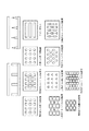
これらのリブからなる隔壁により形成されるセルは、図5に示すごとく、基板平面方向からみて四角状、三角状、ライン状、円形状、六角状が例示され、配置としては格子状やハニカム状や網目状が例示される。表示面側から見える隔壁断面部分に相当する部分(セルの枠部の面積)はできるだけ小さくした方が良く、表示の鮮明さが増す。
ここで、隔壁の形成方法を例示すると、金型転写法、スクリーン印刷法、サンドブラスト法、フォトリソ法、アディティブ法が挙げられる。いずれの方法もこの発明の情報表示装置に搭載する情報表示用パネルに好適に用いることができるが、これらのうち、レジストフィルムを用いるフォトリソ法や金型転写法が好適に用いられる。
The shape of the partition provided on the substrate as required is appropriately set appropriately depending on the type of display medium involved in display, the shape of the electrode to be arranged, and the arrangement, and is not limited in general, but the width of the partition is 2 to 100 μm. The height of the partition wall is adjusted to 10 to 100 μm, preferably 10 to 50 μm.
In forming the partition wall, a both-rib method in which ribs are formed on each of the opposing
As shown in FIG. 5, the cells formed by the partition walls made of these ribs are exemplified by a square shape, a triangular shape, a line shape, a circular shape, and a hexagonal shape as viewed from the plane of the substrate. And a mesh shape. It is better to make the portion corresponding to the cross section of the partition wall visible from the display surface side (the area of the cell frame) as small as possible, and the display becomes clearer.
Examples of the method for forming the partition include a mold transfer method, a screen printing method, a sand blast method, a photolithography method, and an additive method. Any of these methods can be suitably used for an information display panel mounted on the information display device of the present invention, and among these, a photolithography method using a resist film and a mold transfer method are suitably used.
次に、本発明の対象となる情報表示用パネルにおいて表示用粒子で構成され表示媒体として用いる粉流体について説明する。なお、本発明の対象となる情報表示用パネルで用いる粉流体の名称については、本出願人が「電子粉流体(登録商標):登録番号4636931 」の権利を得ている。 Next, the powder fluid that is composed of display particles and used as a display medium in the information display panel that is the subject of the present invention will be described. As for the name of the powder fluid used in the information display panel that is the subject of the present invention, the present applicant has obtained the right of “Electronic Powder Fluid (registered trademark): Registration No. 4636931”.
本発明において表示媒体として用いる「粉流体」は、気体の力も液体の力も借りずに、自ら流動性を示す、流体と粒子の特性を兼ね備えた両者の中間状態の物質である。例えば、液晶は液体と固体の中間的な相と定義され、液体の特徴である流動性と固体の特徴である異方性(光学的性質)を有するものである(平凡社:大百科事典)。一方、粒子の定義は、無視できるほどの大きさであっても有限の質量をもった物体であり、重力の影響を受けるとされている(丸善:物理学事典)。ここで、粒子でも、気固流動層体、液固流動体という特殊状態があり、粒子に底板から気体を流すと、粒子には気体の速度に対応して上向きの力が作用し、この力が重力とつりあう際に、流体のように容易に流動できる状態になるものを気固流動層体と呼び、同じく、流体により流動化させた状態を液固流動体と呼ぶとされている(平凡社:大百科事典)。このように気固流動層体や液固流動体は、気体や液体の流れを利用した状態である。本発明では、このような気体の力も、液体の力も借りずに、自ら流動性を示す状態の物質を、特異的に作り出せることが判明し、これを粉流体と定義した。 The “powder fluid” used as a display medium in the present invention is a substance in an intermediate state between fluid and particles that exhibits fluidity by itself without borrowing the force of gas or liquid. For example, liquid crystal is defined as an intermediate phase between a liquid and a solid, and has fluidity that is a characteristic of liquid and anisotropy (optical properties) that is a characteristic of solid (Heibonsha: Encyclopedia) . On the other hand, the definition of particle is an object with a finite mass even if it is negligible, and is said to be affected by gravity (Maruzen: Physics Encyclopedia). Here, even in the case of particles, there are special states of gas-solid fluidized bed and liquid-solid fluids. When gas is flowed from the bottom plate to the particles, upward force is applied to the particles according to the velocity of the gas. Is a gas-solid fluidized bed that is in a state where it can easily flow when it balances with gravity, and it is also called a liquid-solid fluidized state that is fluidized by a fluid (ordinary) Company: Encyclopedia). As described above, the gas-solid fluidized bed body and the liquid-solid fluid are in a state of using a gas or liquid flow. In the present invention, it has been found that a substance in a state of fluidity can be produced specifically without borrowing the force of such gas and liquid, and this is defined as powder fluid.
すなわち、本発明において表示媒体として用いる粉流体は、液晶(液体と固体の中間相)の定義と同様に、粒子と液体の両特性を兼ね備えた中間的な状態で、先に述べた粒子の特徴である重力の影響を極めて受け難く、高流動性を示す特異な状態を示す物質である。このような物質はエアロゾル状態、すなわち気体中に固体状もしくは液体状の物質が分散質として安定に浮遊する分散系で得ることができ、情報表示用パネルで固体状物質を分散質とするものである。 That is, the pulverulent fluid used as the display medium in the present invention is an intermediate state having both particle and liquid characteristics, similar to the definition of liquid crystal (intermediate phase between liquid and solid). It is a substance that is extremely resistant to the effects of gravity and that exhibits a unique state of high fluidity. Such a substance can be obtained in an aerosol state, that is, in a dispersion system in which a solid or liquid substance is stably suspended as a dispersoid in a gas, and a solid substance is used as a dispersoid in an information display panel. is there.
本発明の対象となる情報表示用パネルは、少なくとも一方が透明な、対向する基板間に、例えば気体中に固体粒子が分散質として安定に浮遊するエアロゾル状態で高流動性を示す粉流体を封入するものであり、このような粉流体は、粉体の流動性を示す指数である安息角を有しないほど流動性に富んだものであり、小さな電界の力でクーロン力などにより容易に安定して移動させることができる。
粉流体とは、先に述べたように、気体の力も液体の力も借りずに、自ら流動性を示す、流体と粒子の特性を兼ね備えた両者の中間状態の物質である。この粉流体は、特にエアロゾル状態とすることができ、本発明の対象となる情報表示用パネルでは、気体中に固体状の物質が分散質として比較的安定に浮遊する状態で表示媒体として用いられる。
The information display panel to which the present invention is applied encloses a powder fluid that exhibits high fluidity in an aerosol state in which at least one is transparent, between opposed substrates, for example, solid particles in gas are stably suspended as a dispersoid Such a pulverulent fluid is so fluid that it does not have an angle of repose, which is an index indicating the fluidity of the powder, and is easily stabilized by Coulomb force with a small electric field force. Can be moved.
As described above, the powdered fluid is a substance in an intermediate state between the fluid and the particle, which exhibits fluidity by itself without borrowing the force of gas or liquid. This powder fluid can be in an aerosol state in particular, and in the information display panel that is the subject of the present invention, a solid substance is used as a display medium in a state where it floats relatively stably as a dispersoid in the gas. .
粒子を負または正に帯電させる方法は、特に限定されないが、コロナ放電法、電極注入法、摩擦法等の粒子を帯電する方法が用いられる。キャリアを用いてブローオフ法により測定した粒子の帯電量が絶対値で10〜100μC/gであることが好ましい。帯電量の絶対値がこの範囲より低いと、電界の変化に対する応答速度が遅くなり、メモリ性も低くなる。帯電量の絶対値がこの範囲より高いと、電極や基板への鏡像力が強すぎ、メモリ性はよいが、電界を反転した場合の表示媒体の反転追随性が悪くなる。
本発明において、帯電量の測定は、以下によって行った。
<ブローオフ測定原理および測定方法>
ブローオフ法においては、両端に網を張った円筒容器中に表示用粒子とキャリアの混合体を入れ、一端から高圧ガスを吹き込んで表示用粒子とキャリアとを分離し、網の目開きから表示用粒子のみをブローオフ(吹き飛ばし)する。このとき、表示用粒子が容器外に持ち去った帯電量と等量で逆の帯電量がキャリアに残る。そして、この電荷による電束の全てはファラデーケージで集められ、この分だけコンデンサは充電される。そこでコンデンサ両端の電位を測定することにより、表示用粒子の電荷量Qは、
Q=CV(C;コンデンサ容量、V;コンデンサ両端の電圧)
として求められる。
ブローオフ帯電量測定装置としては東芝ケミカル社製のTB−200を用いた。本発明では、被測定粒子の帯電量測定にフェライト系キャリアを用いるが、情報表示用パネルに例えば正帯電性の表示用粒子から構成される表示媒体と負帯電性の表示用粒子から構成される表示媒体との2種類の表示媒体を組み合わせて用いる場合にそれぞれの表示媒体を構成する表示用粒子の帯電量を測定するときには同一種類のキャリアを用いる。具体的には、キャリアとして同和鉄粉工業(株)製のDFC100 リンクル(Mn−Mg含有フェライト系)を用いて粒子の帯電量(μC/g)を測定した。
A method of charging the particles negatively or positively is not particularly limited, and a method of charging the particles such as a corona discharge method, an electrode injection method, and a friction method is used. It is preferable that the charge amount of particles measured by a blow-off method using a carrier is 10 to 100 μC / g in absolute value. When the absolute value of the charge amount is lower than this range, the response speed with respect to the change in the electric field is slowed, and the memory property is also lowered. If the absolute value of the charge amount is higher than this range, the image force on the electrode or the substrate is too strong, and the memory property is good, but the reversal followability of the display medium when the electric field is reversed becomes poor.
In the present invention, the charge amount was measured as follows.
<Blow-off measurement principle and measurement method>
In the blow-off method, a mixture of display particles and carriers is placed in a cylindrical container with nets on both ends, and high-pressure gas is blown from one end to separate the display particles and carriers. Blow off only the particles. At this time, the charge amount equivalent to the charge amount of the display particles taken away from the container remains in the carrier. All of the electric flux due to this charge is collected by the Faraday cage, and the capacitor is charged by this amount. Therefore, by measuring the potential across the capacitor, the charge amount Q of the display particles is
Q = CV (C: capacitor capacity, V: voltage across the capacitor)
As required.
As a blow-off charge amount measuring device, TB-200 manufactured by Toshiba Chemical Corporation was used. In the present invention, a ferrite carrier is used to measure the charge amount of the particles to be measured. The information display panel is composed of, for example, a display medium composed of positively chargeable display particles and negatively chargeable display particles. When two types of display media are used in combination with the display medium, the same type of carrier is used when measuring the charge amount of the display particles constituting each display medium. Specifically, the charge amount (μC / g) of the particles was measured using a DFC100 wrinkle (Mn—Mg-containing ferrite system) manufactured by Dowa Iron Powder Industry Co., Ltd. as a carrier.
表示用粒子は、その帯電電荷を保持する必要があるので、体積固有抵抗が1×10¹⁰Ω・cm以上の絶縁性粒子が好ましく、特に体積固有抵抗が1×10¹²Ω・cm以上の絶縁性粒子が好ましい。また、電荷減衰性の遅い粒子がさらに好ましい。 Since the display particles need to retain the charged charge, insulating particles having a volume resistivity of 1 × 10 10 Ω · cm or more are preferable, and in particular, insulation having a volume resistivity of 1 × 10 12 Ω · cm or more is preferable. Are preferred. Further, particles having a slow charge decay property are more preferable.
次に、本発明の対象となる情報表示用パネルにおいて表示媒体を構成する表示用粒子(以下、粒子ともいう)について説明する。表示用粒子は、そのまま該表示用粒子だけで構成して表示媒体としたり、その他の粒子と合わせて構成して表示媒体としたり、粉流体となるように調整、構成して表示媒体としたりして用いられる。
粒子には、その主成分となる樹脂に、必要に応じて、従来と同様に、荷電制御剤、着色剤、無機添加剤等を含ますことができる。以下に、樹脂、荷電制御剤、着色剤、その他添加剤を例示する。
Next, display particles (hereinafter also referred to as particles) constituting the display medium in the information display panel that is the subject of the present invention will be described. The display particles may be composed of the display particles as they are to form a display medium, or may be combined with other particles to form a display medium, or may be adjusted and configured to become a powder fluid to form a display medium. Used.
The particles can contain a charge control agent, a colorant, an inorganic additive, and the like, if necessary, in the resin as the main component, as in the conventional case. Examples of resins, charge control agents, colorants, and other additives will be given below.
樹脂の例としては、ウレタン樹脂、ウレア樹脂、アクリル樹脂、ポリエステル樹脂、アクリルウレタン樹脂、アクリルウレタンシリコーン樹脂、アクリルウレタンフッ素樹脂、アクリルフッ素樹脂、シリコーン樹脂、アクリルシリコーン樹脂、エポキシ樹脂、ポリスチレン樹脂、スチレンアクリル樹脂、ポリオレフィン樹脂、ブチラール樹脂、塩化ビニリデン樹脂、メラミン樹脂、フェノール樹脂、フッ素樹脂、ポリカーボネート樹脂、ポリスルフォン樹脂、ポリエーテル樹脂、ポリアミド樹脂等が挙げられ、2種以上混合することもできる。また、予め重合した樹脂を使用してもよいし、粒子形成の際に重合して樹脂としてもよい。さらに、重合時に複数種の樹脂原料を用いて共重合体としてもよい。特に、基板との付着力を制御する観点と、懸濁重合の容易さから、アクリル樹脂、アクリルフッ素樹脂、ポリスチレン樹脂、スチレンアクリル樹脂が好適である。 Examples of the resin include urethane resin, urea resin, acrylic resin, polyester resin, acrylic urethane resin, acrylic urethane silicone resin, acrylic urethane fluororesin, acrylic fluororesin, silicone resin, acrylic silicone resin, epoxy resin, polystyrene resin, styrene Acrylic resin, polyolefin resin, butyral resin, vinylidene chloride resin, melamine resin, phenol resin, fluororesin, polycarbonate resin, polysulfone resin, polyether resin, polyamide resin and the like can be mentioned, and two or more kinds can be mixed. In addition, a resin polymerized in advance may be used, or a resin may be polymerized at the time of particle formation. Furthermore, it is good also as a copolymer using several types of resin raw materials at the time of superposition | polymerization. In particular, an acrylic resin, an acrylic fluororesin, a polystyrene resin, and a styrene acrylic resin are suitable from the viewpoint of controlling the adhesive force with the substrate and the ease of suspension polymerization.
荷電制御剤としては、特に制限はないが、負荷電制御剤としては例えば、サリチル酸金属錯体、含金属アゾ染料、含金属(金属イオンや金属原子を含む)の油溶性染料、4級アンモニウム塩系化合物、カリックスアレン化合物、含ホウ素化合物(ベンジル酸ホウ素錯体)、ニトロイミダゾール誘導体、負帯電官能基を有するスチレンアクリル樹脂等が挙げられる。正荷電制御剤としては例えば、ニグロシン染料、トリフェニルメタン系化合物、4級アンモニウム塩系化合物、ポリアミン樹脂、イミダゾール誘導体、正帯電官能基を有するスチレンアクリル樹脂等が挙げられる。その他、超微粒子シリカ、超微粒子酸化チタン、超微粒子アルミナ等の金属酸化物、ピリジン等の含窒素環状化合物及びその誘導体や塩、各種有機顔料、フッ素、塩素、窒素等を含んだ樹脂等も荷電制御剤として用いることもできる。 The charge control agent is not particularly limited. Examples of the negative charge control agent include salicylic acid metal complexes, metal-containing azo dyes, metal-containing oil-soluble dyes (including metal ions and metal atoms), and quaternary ammonium salt systems. Examples thereof include compounds, calixarene compounds, boron-containing compounds (benzyl acid boron complexes), nitroimidazole derivatives, and styrene acrylic resins having negatively charged functional groups. Examples of the positive charge control agent include nigrosine dyes, triphenylmethane compounds, quaternary ammonium salt compounds, polyamine resins, imidazole derivatives, and styrene acrylic resins having positively charged functional groups. In addition, metal oxides such as ultrafine silica, ultrafine titanium oxide, ultrafine alumina, nitrogen-containing cyclic compounds such as pyridine and derivatives and salts thereof, various organic pigments, resins containing fluorine, chlorine, nitrogen, etc. are also charged. It can also be used as a control agent.
着色剤としては、以下に例示するような、有機または無機の各種、各色の顔料、染料が使用可能である。 As the colorant, various organic or inorganic pigments and dyes as exemplified below can be used.
黒色着色剤としては、カーボンブラック、酸化銅、二酸化マンガン、アニリンブラック、活性炭等がある。
青色着色剤としては、C.I.ピグメントブルー15:3、C.I.ピグメントブルー15、紺青、コバルトブルー、アルカリブルーレーキ、ビクトリアブルーレーキ、フタロシアニンブルー、無金属フタロシアニンブルー、フタロシアニンブルー部分塩素化物、ファーストスカイブルー、インダンスレンブルーBC等がある。
赤色着色剤としては、ベンガラ、カドミウムレッド、鉛丹、硫化水銀、カドミウム、パーマネントレッド4R、リソールレッド、ピラゾロンレッド、ウォッチングレッド、カルシウム塩、レーキレッドD、ブリリアントカーミン6B、エオシンレーキ、ローダミンレーキB、アリザリンレーキ、ブリリアントカーミン3B、C.I.ピグメントレッド2等がある。
Examples of the black colorant include carbon black, copper oxide, manganese dioxide, aniline black, activated carbon and the like.
Examples of blue colorants include C.I. I. Pigment blue 15: 3, C.I. I.
Examples of red colorants include bengara, cadmium red, red lead, mercury sulfide, cadmium, permanent red 4R, resol red, pyrazolone red, watching red, calcium salt, lake red D, brilliant carmine 6B, eosin lake, rhodamine lake B, Alizarin Lake,
黄色着色剤としては、黄鉛、亜鉛黄、カドミウムイエロー、黄色酸化鉄、ミネラルファーストイエロー、ニッケルチタンイエロー、ネーブルイエロー、ナフトールイエローS、ハンザイエローG、ハンザイエロー10G、ベンジジンイエローG、ベンジジンイエローGR、キノリンイエローレーキ、パーマネントイエローNCG、タートラジンレーキ、C.I.ピグメントイエロー12等がある。
緑色着色剤としては、クロムグリーン、酸化クロム、ピグメントグリーンB、C.I.ピグメントグリーン7、マラカイトグリーンレーキ、ファイナルイエローグリーンG等がある。
橙色着色剤としては、赤色黄鉛、モリブデンオレンジ、パーマネントオレンジGTR、ピラゾロンオレンジ、バルカンオレンジ、インダンスレンブリリアントオレンジRK、ベンジジンオレンジG、インダンスレンブリリアントオレンジGK、C.I.ピグメントオレンジ31等がある。
紫色着色剤としては、マンガン紫、ファーストバイオレットB、メチルバイオレットレーキ等がある。
白色着色剤としては、亜鉛華、酸化チタン、アンチモン白、硫化亜鉛等がある。
Yellow colorants include chrome yellow, zinc yellow, cadmium yellow, yellow iron oxide, mineral first yellow, nickel titanium yellow, navel yellow, naphthol yellow S, Hansa Yellow G, Hansa Yellow 10G, Benzidine Yellow G, Benzidine Yellow GR, Quinoline Yellow Lake, Permanent Yellow NCG, Tartrazine Lake, C.I. I. Pigment Yellow 12 etc.
Examples of green colorants include chrome green, chromium oxide, pigment green B, C.I. I. Pigment Green 7, Malachite Green Lake, Final Yellow Green G, etc.
Examples of the orange colorant include red chrome yellow, molybdenum orange, permanent orange GTR, pyrazolone orange, Vulcan orange, indanthrene brilliant orange RK, benzidine orange G, indanthrene brilliant orange GK, C.I. I. Pigment Orange 31 etc.
Examples of purple colorants include manganese purple, first violet B, and methyl violet lake.
Examples of white colorants include zinc white, titanium oxide, antimony white, and zinc sulfide.
体質顔料としては、バライト粉、炭酸バリウム、クレー、シリカ、ホワイトカーボン、タルク、アルミナホワイト等がある。また、塩基性、酸性、分散、直接染料等の各種染料として、ニグロシン、メチレンブルー、ローズベンガル、キノリンイエロー、ウルトラマリンブルー等がある。 Examples of extender pigments include barite powder, barium carbonate, clay, silica, white carbon, talc, and alumina white. Examples of various dyes such as basic, acidic, disperse, and direct dyes include nigrosine, methylene blue, rose bengal, quinoline yellow, and ultramarine blue.
無機系添加剤の例としては、酸化チタン、亜鉛華、硫化亜鉛、酸化アンチモン、炭酸カルシウム、鉛白、タルク、シリカ、ケイ酸カルシウム、アルミナホワイト、カドミウムイエロー、カドミウムレッド、カドミウムオレンジ、チタンイエロー、紺青、群青、コバルトブルー、コバルトグリーン、コバルトバイオレット、酸化鉄、カーボンブラック、マンガンフェライトブラック、コバルトフェライトブラック、銅粉、アルミニウム粉などが挙げられる。
これらの顔料および無機系添加剤は、単独であるいは複数組み合わせて用いることができる。このうち特に黒色顔料としてカーボンブラックが、白色顔料として酸化チタンが好ましい。上記着色剤を配合して、所望の色の表示用粒子を作製できる。
Examples of inorganic additives include titanium oxide, zinc white, zinc sulfide, antimony oxide, calcium carbonate, lead white, talc, silica, calcium silicate, alumina white, cadmium yellow, cadmium red, cadmium orange, titanium yellow, Examples include bitumen, ultramarine blue, cobalt blue, cobalt green, cobalt violet, iron oxide, carbon black, manganese ferrite black, cobalt ferrite black, copper powder, and aluminum powder.
These pigments and inorganic additives can be used alone or in combination. Of these, carbon black is particularly preferable as the black pigment, and titanium oxide is preferable as the white pigment. By blending the colorant, display particles having a desired color can be produced.
また、本発明で用いる表示用粒子(以下、粒子ともいう)は平均粒子径d(0.5)が、1〜20μmの範囲であり、均一で揃っていることが好ましい。平均粒子径d(0.5)がこの範囲より大きいと表示上の鮮明さに欠け、この範囲より小さいと粒子同士の凝集力が大きくなりすぎるために表示媒体としての移動に支障をきたすようになる。 The display particles used in the present invention (hereinafter also referred to as particles) preferably have an average particle diameter d (0.5) in the range of 1 to 20 μm and are uniform and uniform. If the average particle diameter d (0.5) is larger than this range, the display is not clear. If the average particle diameter d (0.5) is smaller than this range, the cohesive force between the particles becomes too large, which hinders movement as a display medium.
さらに本発明では、各表示用粒子の粒子径分布に関して、下記式に示される粒子径分布Spanを5未満、好ましくは3未満とする。
Span=(d(0.9)−d(0.1))/d(0.5)
(但し、d(0.5)は粒子の50%がこれより大きく、50%がこれより小さいという粒子径をμmで表した数値、d(0.1)はこれ以下の粒子の比率が10%である粒子径をμmで表した数値、d(0.9)はこれ以下の粒子が90%である粒子径をμmで表した数値である。)
Spanを5以下の範囲に納めることにより、各粒子のサイズが揃い、均一な表示媒体としての移動が可能となる。
Further, in the present invention, regarding the particle size distribution of each display particle, the particle size distribution Span represented by the following formula is set to less than 5, preferably less than 3.
Span = (d (0.9) −d (0.1)) / d (0.5)
(However, d (0.5) is a numerical value expressing the particle diameter in μm that 50% of the particles are larger than this and 50% is smaller than this, and d (0.1) is a particle in which the ratio of the smaller particles is 10%. (Numerical value expressed in μm, and d (0.9) is a numerical value expressed in μm for a particle diameter of 90% or less.)
By keeping Span within a range of 5 or less, the size of each particle is uniform, and movement as a uniform display medium becomes possible.
さらにまた、各粒子の相関について、使用した粒子の内、最大径を有する粒子のd(0.5)に対する最小径を有する粒子のd(0.5)の比を50以下、好ましくは10以下とすることが肝要である。たとえ粒子径分布Spanを小さくしたとしても、互いに帯電特性の異なる粒子が互いに反対方向に動くので、互いの粒子サイズが近く、互いの粒子が当量ずつ反対方向に容易に移動できるようにするのが好適であり、それがこの範囲となる。 Furthermore, regarding the correlation between the particles, the ratio of d (0.5) of the particles having the minimum diameter to d (0.5) of the particles having the maximum diameter among the used particles is set to 50 or less, preferably 10 or less. It is essential. Even if the particle size distribution Span is reduced, particles with different charging characteristics move in opposite directions, so that the particle size is close to each other and each particle can be easily moved in the opposite direction by the equivalent amount. This is within this range.
なお、上記の粒子径分布および粒子径は、レーザー回折/散乱法などから求めることができる。測定対象となる粒子にレーザー光を照射すると空間的に回折/散乱光の光強度分布パターンが生じ、この光強度パターンは粒子径と対応関係があることから、粒子径および粒子径分布が測定できる。
ここで、本発明における粒子径および粒子径分布は、体積基準分布から得られたものである。具体的には、Mastersizer2000(Malvern Instruments Ltd.)測定機を用いて、窒素気流中に粒子を投入し、付属の解析ソフト(Mie理論を用いた体積基準分布を基本としたソフト)にて、粒子径および粒子径分布の測定を行なうことができる。
The particle size distribution and the particle size can be obtained from a laser diffraction / scattering method or the like. When laser light is irradiated onto particles to be measured, a light intensity distribution pattern of diffracted / scattered light is spatially generated, and this light intensity pattern has a corresponding relationship with the particle diameter, so that the particle diameter and particle diameter distribution can be measured. .
Here, the particle size and particle size distribution in the present invention are obtained from a volume-based distribution. Specifically, using a Mastersizer2000 (Malvern Instruments Ltd.) measuring instrument, particles are introduced into a nitrogen stream, and the attached analysis software (software based on volume-based distribution using Mie theory) The diameter and particle size distribution can be measured.
さらに、表示用粒子で構成する表示媒体を、気中空間で駆動する情報表示用パネルに適用する場合には、基板間の表示媒体を取り巻く空隙部分の気体の管理が重要であり、表示安定性向上に寄与する。具体的には、空隙部分の気体の湿度について、25℃における相対湿度を60%RH以下、好ましくは50%RH以下とすることが重要である。
この空隙部分とは、図1(a),(b)、図2(a),(b)、図3(a),(b)、図4(a)において、対向する基板1、基板2に挟まれる部分から、電極5、6、表示媒体3の占有部分、隔壁4の占有部分(隔壁を設けた場合)、情報表示用パネルのシール部分を除いた、いわゆる表示媒体が接する気体部分を指すものとする。
空隙部分の気体は、先に述べた湿度領域であれば、その種類は問わないが、乾燥空気、乾燥窒素、乾燥アルゴン、乾燥ヘリウム、乾燥二酸化炭素、乾燥メタンなどが好適である。この気体は、その湿度が保持されるように情報表示用パネルに封入することが必要であり、例えば、表示媒体の充填、情報表示用パネルの組み立てなどを所定湿度環境下にて行い、さらに、外からの湿度侵入を防ぐシール材、シール方法を施すことが肝要である。
Furthermore, when a display medium composed of display particles is applied to an information display panel that is driven in an air space, it is important to manage the gas in the void surrounding the display medium between the substrates, and display stability. Contributes to improvement. Specifically, it is important that the relative humidity at 25 ° C. is 60% RH or less, and preferably 50% RH or less for the humidity of the gas in the gap.
The voids are the opposing substrate 1 and
The gas in the gap is not limited as long as it is in the humidity region described above, but dry air, dry nitrogen, dry argon, dry helium, dry carbon dioxide, dry methane, and the like are preferable. This gas needs to be sealed in an information display panel so that the humidity is maintained, for example, filling a display medium, assembling an information display panel, etc. in a predetermined humidity environment, It is important to apply a sealing material and a sealing method that prevent moisture from entering from the outside.
本発明の対象となる情報表示用パネルにおける基板と基板との間隔は、表示媒体が移動できて、コントラストを維持できればよいが、通常10〜500μm、好ましくは10〜200μmに調整される。
対向する基板間の空間における表示媒体の体積占有率は5〜70%が好ましく、さらに好ましくは5〜60%である。70%を超える場合には表示媒体の移動に支障をきたし、5%未満の場合にはコントラストが不明確となり易い。
The distance between the substrates in the information display panel that is the subject of the present invention is not limited as long as the display medium can be moved and the contrast can be maintained, but is usually adjusted to 10 to 500 μm, preferably 10 to 200 μm.
The volume occupation ratio of the display medium in the space between the opposing substrates is preferably 5 to 70%, more preferably 5 to 60%. If it exceeds 70%, the movement of the display medium is hindered, and if it is less than 5%, the contrast tends to be unclear.
本発明の製造方法により作製する情報表示用パネルは、ノートパソコン、電子手帳、PDA(Personal Digital Assistants )と呼ばれる携帯型情報機器、携帯電話、ハンディターミナル等のモバイル機器の表示部、電子ブック、電子新聞等の電子ペーパー、看板、ポスター、黒板やホワイトボード等の掲示板、電子卓上計算機、家電製品、自動車用品等の表示部、ポイントカード、ICカード等のカード表示部、電子広告、情報ボード、電子POP(Point Of Presence 、Point Of Purchase advertising )、電子値札、電子棚札、電子楽譜、RF−ID機器の表示部のほか、POS端末、カーナビゲーション装置、時計など様々な電子機器の表示部に好適に用いられる。
なお、本発明に係る情報表示用パネルの駆動方式については、パネル自体にスイッチング素子を用いない単純マトリックス駆動型表示用パネルやスタティック駆動型表示用パネル、また、薄膜トランジスタ(TFT)で代表される三端子スイッチング素子あるいは薄膜ダイオード(TFD)で代表される二端子スイッチング素子を用いたアクティブマトリックス駆動型表示用パネルなど、種々のタイプの情報表示用パネルを用いることができる。
The information display panel produced by the manufacturing method of the present invention is a notebook computer, an electronic notebook, a portable information device called PDA (Personal Digital Assistants), a display unit of a mobile device such as a mobile phone or a handy terminal, an electronic book, an electronic Electronic paper such as newspapers, signboards, posters, bulletin boards such as blackboards and whiteboards, electronic desk calculators, display units for home appliances, automobile supplies, card display units such as point cards and IC cards, electronic advertisements, information boards, electronic Suitable for POP (Point Of Presence, Point Of Purchase advertising), electronic price tag, electronic shelf label, electronic score, display part of RF-ID equipment, as well as display part of various electronic equipment such as POS terminal, car navigation device, clock, etc. Used for.
The information display panel driving method according to the present invention includes a simple matrix driving display panel, a static driving display panel that does not use a switching element in the panel itself, and three thin film transistors (TFTs). Various types of information display panels such as an active matrix drive type display panel using a two-terminal switching element represented by a terminal switching element or a thin film diode (TFD) can be used.
1、2 基板
3 表示媒体(粒子群、粉流体)
3W 白色表示媒体
3B 黒色表示媒体
3Wa 表示用白色粒子
3Ba 表示用黒色粒子
4 隔壁
5、6 電極
11 電極間ショート
1, 2
3W
Claims (3)
完成した情報表示用パネルに電極間ショートや電極配線間ショートがあるか否かを検査する検査工程と、
完成した情報表示用パネルに電極間ショートや電極配線間ショートがあった場合に、電極間ショートや電極配線間ショートを有する基板の外側に配置したレーザー式リペア装置から電極間ショートや電極配線間ショートを有する部位に、所定発振波長、所定最大エネルギー、所定最大ピークパワーおよび所定パルス幅を有するレーザー光線を照射することにより、当該電極間ショートや当該電極配線間ショートを除去するショート除去工程と、を行うことを特徴とする情報表示用パネルの製造方法。 It is generated by enclosing a display medium having optical reflectivity and chargeability between the two hollow substrates, at least one of which is transparent, and applying a predetermined voltage between the counter electrodes provided on the substrate. A method for manufacturing an information display panel that displays information such as an image by moving the display medium by applying an electric field to the display medium,
An inspection process for inspecting whether the completed information display panel has a short-circuit between electrodes or a short-circuit between electrode wirings;
When the completed information display panel has a short circuit between electrodes or a short circuit between electrode wirings, a short circuit between electrodes or a short circuit between electrode wirings from a laser-type repair device placed outside the substrate having a short circuit between electrodes or a short circuit between electrode wirings. Performing a short removal process for removing the short circuit between the electrodes and the short circuit between the electrode wirings by irradiating a laser beam having a predetermined oscillation wavelength, a predetermined maximum energy, a predetermined maximum peak power and a predetermined pulse width to the part having A method of manufacturing an information display panel characterized by the above.
Priority Applications (1)
| Application Number | Priority Date | Filing Date | Title |
|---|---|---|---|
| JP2006220925A JP2008046292A (en) | 2006-08-14 | 2006-08-14 | Manufacturing method of information display panel |
Applications Claiming Priority (1)
| Application Number | Priority Date | Filing Date | Title |
|---|---|---|---|
| JP2006220925A JP2008046292A (en) | 2006-08-14 | 2006-08-14 | Manufacturing method of information display panel |
Publications (1)
| Publication Number | Publication Date |
|---|---|
| JP2008046292A true JP2008046292A (en) | 2008-02-28 |
Family
ID=39180105
Family Applications (1)
| Application Number | Title | Priority Date | Filing Date |
|---|---|---|---|
| JP2006220925A Pending JP2008046292A (en) | 2006-08-14 | 2006-08-14 | Manufacturing method of information display panel |
Country Status (1)
| Country | Link |
|---|---|
| JP (1) | JP2008046292A (en) |
Citations (6)
| Publication number | Priority date | Publication date | Assignee | Title |
|---|---|---|---|---|
| JP2000193995A (en) * | 1998-12-28 | 2000-07-14 | Optrex Corp | Inspecting method for liquid crystal display panel |
| JP2003202593A (en) * | 2002-01-04 | 2003-07-18 | Fujitsu Display Technologies Corp | Liquid crystal display device substrate, liquid crystal display device having the same, and method of manufacturing the same |
| JP2003215640A (en) * | 2002-10-17 | 2003-07-30 | Hitachi Ltd | Tft substrate and its wiring correction method, and liquid crystal display |
| WO2005062112A1 (en) * | 2003-12-19 | 2005-07-07 | Bridgestone Corporation | Method for manufacturing information display |
| JP2005252228A (en) * | 2004-02-05 | 2005-09-15 | Sharp Corp | Display device and manufacturing method thereof |
| JP2005331936A (en) * | 2004-04-21 | 2005-12-02 | Bridgestone Corp | Driving method for information display device |
-
2006
- 2006-08-14 JP JP2006220925A patent/JP2008046292A/en active Pending
Patent Citations (6)
| Publication number | Priority date | Publication date | Assignee | Title |
|---|---|---|---|---|
| JP2000193995A (en) * | 1998-12-28 | 2000-07-14 | Optrex Corp | Inspecting method for liquid crystal display panel |
| JP2003202593A (en) * | 2002-01-04 | 2003-07-18 | Fujitsu Display Technologies Corp | Liquid crystal display device substrate, liquid crystal display device having the same, and method of manufacturing the same |
| JP2003215640A (en) * | 2002-10-17 | 2003-07-30 | Hitachi Ltd | Tft substrate and its wiring correction method, and liquid crystal display |
| WO2005062112A1 (en) * | 2003-12-19 | 2005-07-07 | Bridgestone Corporation | Method for manufacturing information display |
| JP2005252228A (en) * | 2004-02-05 | 2005-09-15 | Sharp Corp | Display device and manufacturing method thereof |
| JP2005331936A (en) * | 2004-04-21 | 2005-12-02 | Bridgestone Corp | Driving method for information display device |
Similar Documents
| Publication | Publication Date | Title |
|---|---|---|
| JP2008076848A (en) | Driving method of information display panel | |
| JP2007225875A (en) | Information display device | |
| JP2008009423A (en) | Information display panel | |
| JP2009020359A (en) | Method of driving panel for information display | |
| JP2008046292A (en) | Manufacturing method of information display panel | |
| JP2008224725A (en) | Information displaying panel | |
| JP4925771B2 (en) | Manufacturing method of information display panel | |
| JP2008058474A (en) | Information display panel | |
| JP2008102188A (en) | Information display module | |
| JP5002225B2 (en) | Driving method of information display panel | |
| JP2007310537A (en) | Touch panel integrated information display device | |
| JP2007226530A (en) | Information display device | |
| JP2008076659A (en) | Driving method of panel for information display | |
| JP2007322805A (en) | Information display panel | |
| JP2007193182A (en) | Information display panel | |
| JP2008070756A (en) | Panel for information display and manufacturing method therefor | |
| JP2006309067A (en) | Method for manufacturing information display panel | |
| JP2007322781A (en) | Panel for information display | |
| JP2006293154A (en) | Method for manufacturing panel for information display, and panel for information display | |
| JP2007079394A (en) | Manufacturing method of information display panel | |
| JP2007232767A (en) | Mother substrate for information display | |
| JP2007078785A (en) | Manufacturing method for panel for information display, and display medium charging apparatus used therefor | |
| JP2007163660A (en) | Panel for information display and manufacturing method thereof | |
| JP2006343576A (en) | Method for manufacturing information display panel, and information display panel | |
| JP2008076660A (en) | Driving method for panel for information display |
Legal Events
| Date | Code | Title | Description |
|---|---|---|---|
| A621 | Written request for application examination |
Free format text: JAPANESE INTERMEDIATE CODE: A621 Effective date: 20090728 |
|
| RD03 | Notification of appointment of power of attorney |
Free format text: JAPANESE INTERMEDIATE CODE: A7423 Effective date: 20090728 |
|
| RD04 | Notification of resignation of power of attorney |
Free format text: JAPANESE INTERMEDIATE CODE: A7424 Effective date: 20090728 |
|
| A131 | Notification of reasons for refusal |
Free format text: JAPANESE INTERMEDIATE CODE: A131 Effective date: 20120110 |
|
| A521 | Written amendment |
Free format text: JAPANESE INTERMEDIATE CODE: A523 Effective date: 20120312 |
|
| A131 | Notification of reasons for refusal |
Free format text: JAPANESE INTERMEDIATE CODE: A131 Effective date: 20120626 |
|
| A02 | Decision of refusal |
Free format text: JAPANESE INTERMEDIATE CODE: A02 Effective date: 20130108 |