JP2008010706A - Circuit apparatus, and its manufacturing method - Google Patents
Circuit apparatus, and its manufacturing method Download PDFInfo
- Publication number
- JP2008010706A JP2008010706A JP2006180860A JP2006180860A JP2008010706A JP 2008010706 A JP2008010706 A JP 2008010706A JP 2006180860 A JP2006180860 A JP 2006180860A JP 2006180860 A JP2006180860 A JP 2006180860A JP 2008010706 A JP2008010706 A JP 2008010706A
- Authority
- JP
- Japan
- Prior art keywords
- electrode
- insulating layer
- circuit
- circuit element
- conductive layer
- Prior art date
- Legal status (The legal status is an assumption and is not a legal conclusion. Google has not performed a legal analysis and makes no representation as to the accuracy of the status listed.)
- Withdrawn
Links
Images


Classifications
-
- H—ELECTRICITY
- H01—ELECTRIC ELEMENTS
- H01L—SEMICONDUCTOR DEVICES NOT COVERED BY CLASS H10
- H01L24/00—Arrangements for connecting or disconnecting semiconductor or solid-state bodies; Methods or apparatus related thereto
- H01L24/80—Methods for connecting semiconductor or other solid state bodies using means for bonding being attached to, or being formed on, the surface to be connected
- H01L24/82—Methods for connecting semiconductor or other solid state bodies using means for bonding being attached to, or being formed on, the surface to be connected by forming build-up interconnects at chip-level, e.g. for high density interconnects [HDI]
-
- H—ELECTRICITY
- H01—ELECTRIC ELEMENTS
- H01L—SEMICONDUCTOR DEVICES NOT COVERED BY CLASS H10
- H01L2224/00—Indexing scheme for arrangements for connecting or disconnecting semiconductor or solid-state bodies and methods related thereto as covered by H01L24/00
- H01L2224/01—Means for bonding being attached to, or being formed on, the surface to be connected, e.g. chip-to-package, die-attach, "first-level" interconnects; Manufacturing methods related thereto
- H01L2224/02—Bonding areas; Manufacturing methods related thereto
- H01L2224/04—Structure, shape, material or disposition of the bonding areas prior to the connecting process
- H01L2224/04105—Bonding areas formed on an encapsulation of the semiconductor or solid-state body, e.g. bonding areas on chip-scale packages
-
- H—ELECTRICITY
- H01—ELECTRIC ELEMENTS
- H01L—SEMICONDUCTOR DEVICES NOT COVERED BY CLASS H10
- H01L2224/00—Indexing scheme for arrangements for connecting or disconnecting semiconductor or solid-state bodies and methods related thereto as covered by H01L24/00
- H01L2224/01—Means for bonding being attached to, or being formed on, the surface to be connected, e.g. chip-to-package, die-attach, "first-level" interconnects; Manufacturing methods related thereto
- H01L2224/10—Bump connectors; Manufacturing methods related thereto
- H01L2224/15—Structure, shape, material or disposition of the bump connectors after the connecting process
- H01L2224/16—Structure, shape, material or disposition of the bump connectors after the connecting process of an individual bump connector
-
- H—ELECTRICITY
- H01—ELECTRIC ELEMENTS
- H01L—SEMICONDUCTOR DEVICES NOT COVERED BY CLASS H10
- H01L2224/00—Indexing scheme for arrangements for connecting or disconnecting semiconductor or solid-state bodies and methods related thereto as covered by H01L24/00
- H01L2224/01—Means for bonding being attached to, or being formed on, the surface to be connected, e.g. chip-to-package, die-attach, "first-level" interconnects; Manufacturing methods related thereto
- H01L2224/18—High density interconnect [HDI] connectors; Manufacturing methods related thereto
- H01L2224/19—Manufacturing methods of high density interconnect preforms
-
- H—ELECTRICITY
- H01—ELECTRIC ELEMENTS
- H01L—SEMICONDUCTOR DEVICES NOT COVERED BY CLASS H10
- H01L2224/00—Indexing scheme for arrangements for connecting or disconnecting semiconductor or solid-state bodies and methods related thereto as covered by H01L24/00
- H01L2224/91—Methods for connecting semiconductor or solid state bodies including different methods provided for in two or more of groups H01L2224/80 - H01L2224/90
- H01L2224/92—Specific sequence of method steps
- H01L2224/921—Connecting a surface with connectors of different types
- H01L2224/9212—Sequential connecting processes
- H01L2224/92142—Sequential connecting processes the first connecting process involving a layer connector
- H01L2224/92144—Sequential connecting processes the first connecting process involving a layer connector the second connecting process involving a build-up interconnect
-
- H—ELECTRICITY
- H01—ELECTRIC ELEMENTS
- H01L—SEMICONDUCTOR DEVICES NOT COVERED BY CLASS H10
- H01L2924/00—Indexing scheme for arrangements or methods for connecting or disconnecting semiconductor or solid-state bodies as covered by H01L24/00
- H01L2924/01—Chemical elements
- H01L2924/01005—Boron [B]
-
- H—ELECTRICITY
- H01—ELECTRIC ELEMENTS
- H01L—SEMICONDUCTOR DEVICES NOT COVERED BY CLASS H10
- H01L2924/00—Indexing scheme for arrangements or methods for connecting or disconnecting semiconductor or solid-state bodies as covered by H01L24/00
- H01L2924/01—Chemical elements
- H01L2924/01006—Carbon [C]
-
- H—ELECTRICITY
- H01—ELECTRIC ELEMENTS
- H01L—SEMICONDUCTOR DEVICES NOT COVERED BY CLASS H10
- H01L2924/00—Indexing scheme for arrangements or methods for connecting or disconnecting semiconductor or solid-state bodies as covered by H01L24/00
- H01L2924/01—Chemical elements
- H01L2924/01013—Aluminum [Al]
-
- H—ELECTRICITY
- H01—ELECTRIC ELEMENTS
- H01L—SEMICONDUCTOR DEVICES NOT COVERED BY CLASS H10
- H01L2924/00—Indexing scheme for arrangements or methods for connecting or disconnecting semiconductor or solid-state bodies as covered by H01L24/00
- H01L2924/01—Chemical elements
- H01L2924/01015—Phosphorus [P]
-
- H—ELECTRICITY
- H01—ELECTRIC ELEMENTS
- H01L—SEMICONDUCTOR DEVICES NOT COVERED BY CLASS H10
- H01L2924/00—Indexing scheme for arrangements or methods for connecting or disconnecting semiconductor or solid-state bodies as covered by H01L24/00
- H01L2924/01—Chemical elements
- H01L2924/01029—Copper [Cu]
-
- H—ELECTRICITY
- H01—ELECTRIC ELEMENTS
- H01L—SEMICONDUCTOR DEVICES NOT COVERED BY CLASS H10
- H01L2924/00—Indexing scheme for arrangements or methods for connecting or disconnecting semiconductor or solid-state bodies as covered by H01L24/00
- H01L2924/01—Chemical elements
- H01L2924/01033—Arsenic [As]
-
- H—ELECTRICITY
- H01—ELECTRIC ELEMENTS
- H01L—SEMICONDUCTOR DEVICES NOT COVERED BY CLASS H10
- H01L2924/00—Indexing scheme for arrangements or methods for connecting or disconnecting semiconductor or solid-state bodies as covered by H01L24/00
- H01L2924/01—Chemical elements
- H01L2924/01074—Tungsten [W]
-
- H—ELECTRICITY
- H01—ELECTRIC ELEMENTS
- H01L—SEMICONDUCTOR DEVICES NOT COVERED BY CLASS H10
- H01L2924/00—Indexing scheme for arrangements or methods for connecting or disconnecting semiconductor or solid-state bodies as covered by H01L24/00
- H01L2924/01—Chemical elements
- H01L2924/01076—Osmium [Os]
-
- H—ELECTRICITY
- H01—ELECTRIC ELEMENTS
- H01L—SEMICONDUCTOR DEVICES NOT COVERED BY CLASS H10
- H01L2924/00—Indexing scheme for arrangements or methods for connecting or disconnecting semiconductor or solid-state bodies as covered by H01L24/00
- H01L2924/01—Chemical elements
- H01L2924/01078—Platinum [Pt]
-
- H—ELECTRICITY
- H01—ELECTRIC ELEMENTS
- H01L—SEMICONDUCTOR DEVICES NOT COVERED BY CLASS H10
- H01L2924/00—Indexing scheme for arrangements or methods for connecting or disconnecting semiconductor or solid-state bodies as covered by H01L24/00
- H01L2924/013—Alloys
- H01L2924/014—Solder alloys
-
- H—ELECTRICITY
- H01—ELECTRIC ELEMENTS
- H01L—SEMICONDUCTOR DEVICES NOT COVERED BY CLASS H10
- H01L2924/00—Indexing scheme for arrangements or methods for connecting or disconnecting semiconductor or solid-state bodies as covered by H01L24/00
- H01L2924/30—Technical effects
- H01L2924/35—Mechanical effects
- H01L2924/351—Thermal stress
Abstract
Description
本発明は、回路装置およびその製造方法に関し、特に配線基板の上に回路素子を搭載した回路装置およびその製造方法に関する。 The present invention relates to a circuit device and a manufacturing method thereof, and more particularly to a circuit device in which a circuit element is mounted on a wiring board and a manufacturing method thereof.
携帯電話、PDA、DVC、DSCといったポータブルエレクトロニクス機器の高機能化が加速するなか、こうした製品が市場で受け入れられるためには小型・軽量化が必須となっており、その実現のために高集積のシステムLSIが求められている。一方、これらのエレクトロニクス機器に対しては、より使い易く便利なものが求められており、機器に使用されるLSIに対し、高機能化、高性能化が要求されている。このため、LSIチップの高集積化にともないそのI/O数が増大する一方でパッケージ自体の小型化要求も強く、これらを両立させるために、半導体部品の高密度な基板実装に適合した半導体パッケージの開発が強く求められている。こうした要求に対応するため、CSP(Chip Size Package)と呼ばれるパッケージ技術が種々開発されている。 As portable electronics devices such as mobile phones, PDAs, DVCs, and DSCs are accelerating their functions, miniaturization and weight reduction are indispensable for these products to be accepted in the market. There is a need for a system LSI. On the other hand, these electronic devices are required to be easier to use and convenient, and higher functionality and higher performance are required for LSIs used in the devices. For this reason, as the number of I / Os increases with higher integration of LSI chips, there is a strong demand for miniaturization of the package itself. In order to achieve both of these, a semiconductor package suitable for high-density board mounting of semiconductor components Development is strongly demanded. In order to meet such demands, various package technologies called CSP (Chip Size Package) have been developed.
このCSPでは一主面に外部接続電極(電極パッド)が形成されたウエハをダイシングすることによりパッケージが形成される。このため、CSPはLSIと同等のサイズにて配線基板(実装基板)に固着することが可能となり、CSPが実装される側の配線基板を小型化することが可能となる。したがって、CSPを採用することにより、ポータブルエレクトロニクス機器のセット全体を小型化することも可能となる。 In this CSP, a package is formed by dicing a wafer having external connection electrodes (electrode pads) formed on one main surface. Therefore, the CSP can be fixed to the wiring board (mounting board) with the same size as the LSI, and the wiring board on the side where the CSP is mounted can be downsized. Therefore, by adopting CSP, the entire set of portable electronic devices can be reduced in size.
一般に、CSPとしての回路素子を配線基板の上に搭載するには、回路素子と配線基板のそれぞれの電極パッドをはんだ等からなる金属バンプを介してフリップチップ接続することにより行う(特許文献1参照)。図6は配線基板上に回路素子を実装した従来の回路装置の構造を概略的に示した断面図である。回路素子(半導体素子)101の表面周辺部に第1電極パッド102が形成され、この回路素子101を搭載するための配線基板108の表面に第2電極パッド109が形成され、はんだからなる金属バンプ114を用いて接着されている。
しかしながら、上述した従来の回路装置では、第1電極パッド102から第2電極パッド109までに至る経路が異なる材料から成るため、接続信頼性に劣る問題があった。具体的には、バンプ114にははんだが採用され、各電極パッド(第1電極パッド102、第2電極パッド109)は一般的に銅から成る。このため、バンプ114と各電極パッドとでは材料が異なるため、温度変化に応じて両者の界面には熱応力が発生する。したがって、バンプ114と各電極パッドとの接合箇所で断線が発生する恐れがあった。
However, the conventional circuit device described above has a problem of poor connection reliability because the path from the
また、従来の回路装置をプリント実装基板に実装する際(具体的には、回路装置の配線基板108の裏面側の電極をプリント実装基板上の電極と接続固定する際)に加わる熱処理によって、回路装置内のバンプ114が体積膨張し、回路装置内で剥離の起点となることがあるため、回路装置を実装したプリント実装基板の信頼性が劣化する問題がある。
In addition, when the conventional circuit device is mounted on the printed mounting board (specifically, when the electrode on the back side of the
本発明はこうした状況に鑑みてなされたものであり、その目的は、配線基板とその上に搭載する回路素子との間の接続信頼性に優れた回路装置およびその製造技術を提供することにある。 The present invention has been made in view of such circumstances, and an object of the present invention is to provide a circuit device excellent in connection reliability between a wiring board and a circuit element mounted thereon and a manufacturing technique thereof. .
上記課題を解決するために、本発明に係る回路装置は、第1の電極を有する回路素子と、第2の電極を有する配線基板と、配線基板上に設けられた絶縁層と、第2の電極から絶縁層内に、この第2の電極と一体的に設けられた導体部と、を備え、絶縁層上に回路素子が設置され、この状態で第1の電極と導体部とが接続されていることを特徴とする。 In order to solve the above problems, a circuit device according to the present invention includes a circuit element having a first electrode, a wiring board having a second electrode, an insulating layer provided on the wiring board, A conductor part integrally provided with the second electrode in the insulating layer from the electrode, and a circuit element is installed on the insulating layer, and in this state, the first electrode and the conductor part are connected to each other. It is characterized by.
この発明によれば、回路装置をプリント実装基板上に実装する際に加わる熱処理によって発生する配線基板と回路素子との剥離による断線などを抑制することができる。このため、回路装置の耐熱信頼性(配線基板とその上に搭載する回路素子との間の接続信頼性)が向上する。これは、第2の電極と導体部とを一体化して形成しているため、その部分に接合界面がなくなり、従来のはんだ等の金属バンプを用いた場合に発生する体積膨張に起因した応力負荷が抑制されるためである。 According to the present invention, it is possible to suppress disconnection due to peeling between the wiring board and the circuit element, which is generated by heat treatment applied when the circuit device is mounted on the printed mounting board. For this reason, the heat resistance reliability (connection reliability between a wiring board and a circuit element mounted thereon) is improved. This is because the second electrode and the conductor portion are integrally formed, so that there is no joint interface at that portion, and the stress load caused by the volume expansion that occurs when using conventional metal bumps such as solder This is because it is suppressed.
上記構成において、第1の電極および導体部とは同一の金属からなることが好ましい。この構成によれば、第1の電極と導体部との熱膨張係数が同じになるので、回路装置の熱応力に対する接続信頼性(耐熱信頼性)をさらに向上させることができる。 In the above configuration, the first electrode and the conductor portion are preferably made of the same metal. According to this configuration, since the thermal expansion coefficients of the first electrode and the conductor portion are the same, the connection reliability (heat resistance reliability) against the thermal stress of the circuit device can be further improved.
上記課題を解決するために、本発明に係る回路装置の製造方法は、第1の電極を有する回路素子を用意する第1の工程と、第1の絶縁層の一方の面側に回路素子の第1の電極を有する面を圧着する第2の工程と、第1の絶縁層に、その他方の面側から第1の電極が露出するように開口部を形成する第3の工程と、開口部内を含む絶縁層上に、第1の電極と接続する第1の導電層を形成する第4の工程と、第1の絶縁層の他方の面側に、少なくとも一層の第2の絶縁層と第2の導電層との積層構造からなる配線基板を形成する第5の工程と、を備え、第1の導電層の一部は配線基板の第2の電極として機能することを特徴とする。 In order to solve the above problems, a method of manufacturing a circuit device according to the present invention includes a first step of preparing a circuit element having a first electrode, and a circuit element on one surface side of the first insulating layer. A second step of pressure-bonding the surface having the first electrode; a third step of forming an opening in the first insulating layer so that the first electrode is exposed from the other surface side; A fourth step of forming a first conductive layer connected to the first electrode on the insulating layer including the inside of the portion; and at least one second insulating layer on the other surface side of the first insulating layer; And a fifth step of forming a wiring substrate having a laminated structure with the second conductive layer, wherein a part of the first conductive layer functions as a second electrode of the wiring substrate.
この発明によれば、回路素子の第1の電極と配線基板とが第1の導電層を介して接続され、従来のはんだバンプを介した接続に比べて、熱応力に対する接続信頼性(耐熱信頼性)が向上した回路装置が容易に製造される。 According to the present invention, the first electrode of the circuit element and the wiring board are connected via the first conductive layer, and the connection reliability against heat stress (heat resistance reliability) is compared with the connection via the conventional solder bump. The circuit device with improved characteristics is easily manufactured.
上記構成において、第1の電極および第1の導電層は同一の材料からなるように製造することが好ましい。この構成によれば、第1の電極と第1の導電層との熱膨張係数を容易に同じとすることができるので、熱応力に対する接続信頼性(耐熱信頼性)がさらに向上した回路装置を製造することができる。 In the above structure, the first electrode and the first conductive layer are preferably manufactured to be made of the same material. According to this configuration, since the thermal expansion coefficients of the first electrode and the first conductive layer can be easily made the same, a circuit device with further improved connection reliability (heat resistance reliability) against thermal stress can be obtained. Can be manufactured.
本発明によれば、配線基板とその上に搭載する回路素子との間の接続信頼性に優れた回路装置およびその製造技術が提供される。 ADVANTAGE OF THE INVENTION According to this invention, the circuit apparatus excellent in the connection reliability between a wiring board and the circuit element mounted on it and its manufacturing technique are provided.
以下、本発明を具現化した実施形態について図面に基づいて説明する。なお、すべての図面において、同様な構成要素には同様の符号を付し、適宜説明を省略する。 DESCRIPTION OF EXEMPLARY EMBODIMENTS Hereinafter, embodiments of the invention will be described with reference to the drawings. In all the drawings, the same reference numerals are given to the same components, and the description will be omitted as appropriate.
(第1実施形態)
図1は本発明の第1実施形態に係る回路装置の概略断面図である。図1に基づいて第1実施形態の回路装置について説明する。
(First embodiment)
FIG. 1 is a schematic cross-sectional view of a circuit device according to a first embodiment of the present invention. The circuit device according to the first embodiment will be described with reference to FIG.
この第1実施形態での回路装置は、その表面に電極4aを有する回路素子5と、その表面に電極7cを有する配線基板12と、配線基板12と回路素子5との間に設けられた絶
縁層6と、この絶縁層6を貫通し、電極4aと電極7cとを接続する導体部8を備えている。なお、電極4aは本発明の「第1の電極」および電極7cは本発明の「第2の電極」の一例である。
The circuit device according to the first embodiment includes a
回路素子5は、P型シリコン基板などの半導体基板1の表面(下面側)に周知の技術により所定の電気回路(図示せず)が形成され、実装面となる表面(特に周辺部)に電極3が形成されている。この電極3を除いた半導体基板1の表面上の領域には保護膜2が形成されている。さらに電極3のピッチをより広くするために、電極3に接続して再配線パターン4および再配線された電極4aが形成されている。
The
配線基板12は、絶縁層9、絶縁層9の上面側に形成された電極7cを含む導電層7、及び絶縁層9の下面側に形成された導電層10からなる積層構造を有する。上下の導電層はビアホール9a内に設けられた導体部11によって接続されている。この絶縁層9にはエポキシ樹脂を主成分とする膜が採用され、その厚さは、たとえば、約100μmである。また、導電層7,10には銅(Cu)等の金属が採用され、その厚さは、たとえば、約30μmである。
The wiring substrate 12 has a laminated structure including the
絶縁層6は、回路素子5と配線基板12との間に設けられている。絶縁層6にはエポキシ樹脂を主成分とする膜が採用され、その厚さは、たとえば、約100μmである。なお、エポキシ樹脂を主成分とする絶縁層6は、編み込まれたガラス繊維に樹脂を含浸させたタイプの膜であってもよい。あるいは、絶縁層6に約2μm〜10μm程度の直径を有するフィラーが添加された膜であってもよい。このフィラーとしては、アルミナ(Al2O3)、シリカ(SiO2)、窒化アルミニウム(AlN)、窒化シリコン(SiN)および窒化ホウ素(BN)などがある。また、フィラーの重量充填率は約30%〜約80%である。
The
導体部8は絶縁層6を貫通して形成された開口部6a内に設けられ、回路素子5の電極4aと配線基板12の電極7cとを電気的に接続している。ここで、導体部8は導電層7の電極7cと一体的に設けられている。
(製造方法)
図2〜図4は、図1に示した第1実施形態による回路装置の製造プロセスを説明するための断面図である。次に、図1〜図4を参照して、第1実施形態による回路装置の製造プロセスについて説明する。
The
(Production method)
2 to 4 are cross-sectional views for explaining a manufacturing process of the circuit device according to the first embodiment shown in FIG. Next, the manufacturing process of the circuit device according to the first embodiment will be described with reference to FIGS.
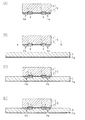
図2(A)に示すように、その表面に電極4aを有する回路素子5を用意する。具体的には、P型シリコン基板などの半導体基板1の表面(下面側)に周知の技術により所定の電気回路(図示せず)およびその周辺部あるいは上部に電極3を形成する。電極3の材料には一般的にアルミニウム(Al)等の金属が採用される。この電極3を除いた半導体基板1の表面上の領域に、半導体基板1を保護するための絶縁性の保護膜2を形成する。保護膜2としてはシリコン酸化膜(SiO2)やシリコン窒化膜(SiN)等が採用される。さらに電極3のピッチをより広くするために銅からなる再配線パターン4および電極4aを形成する。ここでは、レジストパターン形成、銅めっき処理、及びレジスト除去を2回繰り返して所望の再配線パターン4および電極4aを形成している。
As shown in FIG. 2A, a
図2(B)に示すように、回路素子5よりも面積の大きな銅箔7a付きの絶縁層6に対して回路素子5をその表面(下面側)から真空下または減圧下で熱圧着する。なお、絶縁層6の厚さは、たとえば、約100μmとし、銅箔7aの厚さは、たとえば、約10μmとする。絶縁層6としては先に示した材料が採用される。
As shown in FIG. 2B, the
回路素子5を絶縁層6に圧着することにより、図2(C)に示すように、絶縁層6内に
回路素子5の電極4aを含む再配線パターン4が埋め込まれ、絶縁層6上に回路素子5が固着される。
By pressing the
図2(D)に示すように、フォトリソグラフィ技術およびエッチング技術を用いて開口部6a(図1参照)の形成領域に位置する銅箔7aを除去する。これにより、絶縁層6の開口部6aの形成領域が露出される。
As shown in FIG. 2D, the
次に、図3(A)に示すように、銅箔7aの下方から炭酸ガスレーザまたはUVレーザを照射することによって、絶縁層6の露出した表面から電極4aの表面に達するまでの領域を除去する。これにより、絶縁層6に、約70μmの直径を有し、絶縁層6を貫通する開口部6aを形成する。なお、絶縁層6は本発明の「第1の絶縁層」の一例である。
Next, as shown in FIG. 3A, the region from the exposed surface of the insulating
図3(B)に示すように、無電解めっき法を用いて、銅箔7aの表面および開口部6aの内面上に銅を約0.5μmの厚みでめっきする。続いて、電解めっき法を用いて、銅箔7aの表面および開口部6aの内部に銅をめっきする。なお、本実施形態では、めっき液中に抑制剤および促進剤を添加することによって、抑制剤を銅箔7aの表面上に吸着させるとともに、促進剤を開口部6aの内面上に吸着させる。これにより、開口部6aの内面上の銅めっきの厚みを大きくすることができるので、開口部6a内に銅を埋め込むことができる。その結果、図3(B)に示すように、絶縁層6上に約30μmの厚みを有する導電層7bが形成されるとともに、開口部6a内に導体部8が埋め込み形成される。
As shown in FIG. 3B, copper is plated to a thickness of about 0.5 μm on the surface of the
図3(C)に示すように、フォトリソグラフィ技術およびエッチング技術を用いて、導電層7bをパターニングする。これにより、電極7cおよび所定の配線パターンを含む導電層7が形成される。なお、導電層7および導体部8は本発明の「第1の導電層」の一例である。
As shown in FIG. 3C, the conductive layer 7b is patterned by using a photolithography technique and an etching technique. Thereby, the
図3(D)に示すように、銅箔10a付きの絶縁層9を絶縁層6の下面側から真空下または減圧下で熱圧着する。ここで、絶縁層9の厚さは、たとえば、約100μmとし、銅箔10aの厚さは、たとえば、約10μmとする。絶縁層9としては先に示した絶縁層6と同じ材料が採用される。なお、絶縁層9は本発明の「第2の絶縁層」の一例である。
As shown in FIG. 3D, the insulating
銅箔10a付き絶縁層9を圧着することにより、図4(A)に示すように、絶縁層9内に導電層7が埋め込まれる。これにより、絶縁層6の下面側に配線基板12(図1参照)の基材となる部分が形成される。
By crimping the insulating
図4(B)に示すように、フォトリソグラフィ技術およびエッチング技術を用いてビアホール9a(図1参照)の形成領域に位置する銅箔10aを除去する。これにより、絶縁層9のビアホール9aの形成領域が露出される。
As shown in FIG. 4B, the
図4(C)に示すように、銅箔10aの下方から炭酸ガスレーザまたはUVレーザを照射することによって、絶縁層9の露出した表面から導電層7の表面に達するまでの領域を除去する。これにより、絶縁層9に、約70μmの直径を有し、絶縁層9を貫通するビアホール9aを形成する。
As shown in FIG. 4C, a region from the exposed surface of the insulating
図4(D)に示すように、無電解めっき法を用いて、銅箔10aの表面およびビアホール9aの内面上に銅を約0.5μmの厚みでめっきする。続いて、電解めっき法を用いて、銅箔10aの表面およびビアホール9aの内部に銅をめっきする。なお、本実施形態では、めっき液中に抑制剤および促進剤を添加することによって、抑制剤を銅箔10aの表面上に吸着させるとともに、促進剤をビアホール9aの内面上に吸着させる。これにより、ビアホール9aの内面上の銅めっきの厚みを大きくすることができるので、ビアホール
9a内に銅を埋め込むことができる。その結果、図4(D)に示すように、絶縁層9上に約30μmの厚みを有する導電層10bが形成されるとともに、ビアホール9a内に導体部11が埋め込み形成される。
As shown in FIG. 4D, copper is plated to a thickness of about 0.5 μm on the surface of the
最後に、図1に示したように、フォトリソグラフィ技術およびエッチング技術を用いて、導電層10bをパターニングする。これにより、所定の配線パターンを有する導電層10が形成される。この結果、基材としての絶縁層9、この絶縁層9の上面側に形成された電極7cを含む導電層7、及び絶縁層9の下面側に形成された導電層10の積層構造を有する配線基板12が形成される。なお、導電層10は本発明の「第2の導電層」の一例である。
Finally, as shown in FIG. 1, the
これらの工程により、第1実施形態の回路装置が製造される。 Through these steps, the circuit device of the first embodiment is manufactured.
以上説明した第1実施形態の回路装置およびその製造方法によれば、以下のような効果を得ることができるようになる。
(1)回路装置をプリント実装基板上に実装する際、回路装置に加わる熱処理によって発生する配線基板12と回路素子5との剥離による断線などを抑制することができる。このため、回路装置の耐熱信頼性(配線基板12とその上に搭載する回路素子5との間の接続信頼性)が向上する。これは、配線基板12の電極7cと導体部8とを一体化して形成したため、その部分に接合界面がなくなり、従来のはんだ等の金属バンプを用いた場合に発生する体積膨張に起因した応力負荷が抑制されるためである。
(2)電極7cと導体部8とが一体化された金属で形成したことで、電極7cと導体部8との間に接合界面がなくなるので、使用状況下の温度変化等により熱応力が作用しても断線等は生じず、熱応力に対する回路装置の接続信頼性を向上させることができる。
(3)電極4aと導体部8とを同一の金属としたことで、電極4aと導体部8との熱膨張係数が同じなるので、使用状況下の温度変化等によりこの部分に熱応力が作用しても断線等の恐れが少ない構成となる。この結果、熱応力に対する回路装置の接続信頼性をさらに向上させることができる。
(4)回路素子5の電極4aと配線基板12とが導体部8と一体化した導電層7を介して接続され、従来のはんだバンプを介した接続に比べて、熱応力に対する接続信頼性が向上した回路装置が容易に製造される。
(5)電極4aおよび導電層7(特に導体部8)を同一の材料で製造したことで、電極4aと導電層7(特に導体部8)との熱膨張係数を容易に同じとすることができるので、熱応力に対する接続信頼性がさらに向上した回路装置を製造することができるようになる。(6)回路素子5と配線基板12とを接続する導体部8および絶縁層6の製造を、配線基板12を構成する絶縁層9および導電層10と同じプロセスをそのまま採用して形成できるので、新たな設備投資をすることなく、低コストで回路装置を製造することができる。(7)回路素子5と配線基板12との間の間隔を絶縁層6の膜厚により容易に制御できるので、回路装置の薄型化を容易に実現することができる。
According to the circuit device and the manufacturing method thereof according to the first embodiment described above, the following effects can be obtained.
(1) When the circuit device is mounted on the printed circuit board, disconnection due to peeling between the wiring board 12 and the
(2) Since the
(3) Since the
(4) The
(5) Since the
(第2実施形態)
図5は本発明の第2実施形態に係る概略断面図である。第1実施形態と異なる箇所は、回路素子5に第1実施形態での再配線パターン4および電極4aを設けず、配線基板12aと接続する導体部8aが半導体基板1上の電極3と直接接続していることである。それ以外については、第1実施形態と同様である。
(Second Embodiment)
FIG. 5 is a schematic cross-sectional view according to the second embodiment of the present invention. The difference from the first embodiment is that the
この第2実施形態の回路装置およびその製造方法によれば、以下のような効果を得ることができるようになる。
(8)従来、半導体基板1上の電極3間のピッチは、たとえば、約70μmと非常に狭く、このままでははんだバンプ接続が困難であるため、回路素子の小型化を犠牲にして半導体基板1上に再配線パターンおよびそれに連結して設けられた電極を形成していた。これ
により、再配線後の電極間のピッチは約500μmとなり、はんだバンプ接続を容易に行えるようにしていた。この実施形態によれば、半導体基板1の電極3を再配線することなく、回路素子5と配線基板12aとを接続することができるので、再配線パターン部分の領域削減による回路素子5の小型化、さらには回路装置の小型化を実現することができる。
According to the circuit device and the manufacturing method thereof of the second embodiment, the following effects can be obtained.
(8) Conventionally, the pitch between the
なお、上記実施形態では、配線基板上に1つの回路素子を搭載した回路装置の例を示したが、本発明はこれに限らず、たとえば、図2(B)で示した工程において絶縁層上に複数の回路素子を圧着してもよい。この場合、配線基板とそれぞれの回路素子との間で熱応力に対する接続信頼性を向上させることができるようになる。 In the above embodiment, an example of a circuit device in which one circuit element is mounted on a wiring board has been shown. However, the present invention is not limited to this, and for example, on the insulating layer in the process shown in FIG. A plurality of circuit elements may be pressure-bonded to each other. In this case, the connection reliability against thermal stress can be improved between the wiring board and each circuit element.
上記実施形態では、配線基板上に1つの回路素子を搭載した回路装置の製造方法の例を示したが、本発明はこれに限らず、たとえば、回路素子を個別に切断する前のウエハ状態の半導体基板(回路素子となる部分がアレイ状に複数の形成された半導体基板)を絶縁層上に圧着し、上記と同様の工程を経て配線基板部分を形成した後、それをダイシングにより個別に切断して複数の回路装置を製造してもよい。この場合にも個々の回路装置は上記効果を享受することができる。 In the above-described embodiment, an example of a method of manufacturing a circuit device in which one circuit element is mounted on a wiring board has been shown. However, the present invention is not limited to this, and for example, a wafer state before the circuit elements are individually cut. A semiconductor substrate (semiconductor substrate on which a plurality of circuit element portions are formed in an array) is pressure-bonded onto an insulating layer, a wiring substrate portion is formed through the same process as described above, and then cut individually by dicing. Thus, a plurality of circuit devices may be manufactured. Even in this case, each circuit device can enjoy the above-described effect.
上記実施形態では、基材としての絶縁層9、この絶縁層の9上面側に形成された電極7cを含む導電層7、及び絶縁層9の下面側に形成された導電層10の2層配線構造の配線基板12の例を示したが、本発明はこれに限らず、たとえば、絶縁層9の下面側にさらに絶縁層および配線層を交互に積層した多層配線構造の配線基板としてもよい。
In the above embodiment, the two-layer wiring of the insulating
上記実施形態では、回路素子5に再配線パターン4および電極4aを形成した例を示したが、本発明はこれに限らず、たとえば、再配線パターン4のみを形成するだけでもよい。また、その形成は、保護膜2上に樹脂層を貼り付け、この樹脂層にレーザ加工によって開口部を形成し、その開口部に銅めっき処理を行い、最後にエッチングして所望の再配線パターンに加工する方法で行ってもよい。
In the above-described embodiment, an example in which the
1・・・半導体基板、2・・・保護膜、3・・・電極、4・・・再配線パターン、4a・・・電極、5・・・回路素子、6・・・絶縁層、6a・・・開口部、7・・・導電層、7c・・・電極、8・・・導体部、9・・・絶縁層、9a・・・ビアホール、10・・・導電層、11・・・導体部、12・・・配線基板 DESCRIPTION OF SYMBOLS 1 ... Semiconductor substrate, 2 ... Protective film, 3 ... Electrode, 4 ... Rewiring pattern, 4a ... Electrode, 5 ... Circuit element, 6 ... Insulating layer, 6a ..Opening portion, 7 ... conductive layer, 7c ... electrode, 8 ... conductor portion, 9 ... insulating layer, 9a ... via hole, 10 ... conductive layer, 11 ... conductor Part, 12 ... wiring board
Claims (4)
第2の電極を有する配線基板と、
前記配線基板上に設けられた絶縁層と、
前記第2の電極から前記絶縁層内に、この第2の電極と一体的に設けられた導体部と、を備え、
前記絶縁層上に前記回路素子が設置され、この状態で前記第1の電極と前記導体部とが接続されている回路装置。 A circuit element having a first electrode;
A wiring board having a second electrode;
An insulating layer provided on the wiring board;
A conductor portion provided integrally with the second electrode in the insulating layer from the second electrode,
A circuit device in which the circuit element is installed on the insulating layer, and the first electrode and the conductor are connected in this state.
第1の絶縁層の一方の面側に前記回路素子の前記第1の電極を有する面を圧着する第2の工程と、
前記第1の絶縁層に、その他方の面側から前記第1の電極が露出するように開口部を形成する第3の工程と、
前記開口部内を含む前記絶縁層上に、前記第1の電極と接続する第1の導電層を形成する第4の工程と、
前記第1の絶縁層の他方の面側に、少なくとも一層の第2の絶縁層と第2の導電層との積層構造からなる配線基板を形成する第5の工程と、
を備え、
前記第1の導電層の一部は前記配線基板の第2の電極として機能することを特徴とした回路装置の製造方法。 A first step of preparing a circuit element having a first electrode;
A second step of pressure bonding the surface of the circuit element having the first electrode to one surface side of the first insulating layer;
A third step of forming an opening in the first insulating layer so that the first electrode is exposed from the other surface side;
A fourth step of forming a first conductive layer connected to the first electrode on the insulating layer including the inside of the opening;
A fifth step of forming a wiring substrate having a laminated structure of at least one second insulating layer and a second conductive layer on the other surface side of the first insulating layer;
With
A part of said 1st conductive layer functions as a 2nd electrode of the said wiring board, The manufacturing method of the circuit apparatus characterized by the above-mentioned.
Priority Applications (1)
| Application Number | Priority Date | Filing Date | Title |
|---|---|---|---|
| JP2006180860A JP2008010706A (en) | 2006-06-30 | 2006-06-30 | Circuit apparatus, and its manufacturing method |
Applications Claiming Priority (1)
| Application Number | Priority Date | Filing Date | Title |
|---|---|---|---|
| JP2006180860A JP2008010706A (en) | 2006-06-30 | 2006-06-30 | Circuit apparatus, and its manufacturing method |
Publications (2)
| Publication Number | Publication Date |
|---|---|
| JP2008010706A true JP2008010706A (en) | 2008-01-17 |
| JP2008010706A5 JP2008010706A5 (en) | 2009-08-13 |
Family
ID=39068635
Family Applications (1)
| Application Number | Title | Priority Date | Filing Date |
|---|---|---|---|
| JP2006180860A Withdrawn JP2008010706A (en) | 2006-06-30 | 2006-06-30 | Circuit apparatus, and its manufacturing method |
Country Status (1)
| Country | Link |
|---|---|
| JP (1) | JP2008010706A (en) |
-
2006
- 2006-06-30 JP JP2006180860A patent/JP2008010706A/en not_active Withdrawn
Similar Documents
| Publication | Publication Date | Title |
|---|---|---|
| JP6263573B2 (en) | Multilayer electronic device and manufacturing method thereof | |
| JP4503039B2 (en) | Circuit equipment | |
| TWI476888B (en) | Package substrate having embedded via hole medium layer and fabrication method thereof | |
| JP4467489B2 (en) | Circuit board and circuit device using the same | |
| JP4345808B2 (en) | Manufacturing method of semiconductor device | |
| JP5091221B2 (en) | Semiconductor device | |
| US9338886B2 (en) | Substrate for mounting semiconductor, semiconductor device and method for manufacturing semiconductor device | |
| US8288865B2 (en) | Semiconductor module having semiconductor device mounted on device mounting substrate | |
| JP5367523B2 (en) | Wiring board and method of manufacturing wiring board | |
| JP2005322858A (en) | Method for manufacturing semiconductor device | |
| JP2005286036A (en) | Electronic component packaging structure and its manufacturing method | |
| JP2009206525A (en) | Method for manufacturing wiring substrate | |
| JP2008028376A (en) | Circuit board, semiconductor module and method of manufacturing circuit board | |
| WO2005114728A1 (en) | Semiconductor device, wiring board and manufacturing method thereof | |
| JPWO2006100909A1 (en) | Semiconductor device and manufacturing method thereof | |
| JP5173758B2 (en) | Manufacturing method of semiconductor package | |
| JP4900624B2 (en) | Circuit equipment | |
| JP2008210912A (en) | Semiconductor device and its manufacturing method | |
| JP4844392B2 (en) | Semiconductor device and wiring board | |
| JP2008135553A (en) | Substrate laminating method and semiconductor device in which substrates are laminated | |
| JP2007317955A (en) | Circuit module board incorporating components | |
| JP2008218521A (en) | Circuit device and method for manufacturing the same | |
| JP4467540B2 (en) | Circuit equipment | |
| JP2010092974A (en) | Semiconductor device and method of manufacturing the same, and electronic device | |
| JP2008010706A (en) | Circuit apparatus, and its manufacturing method |
Legal Events
| Date | Code | Title | Description |
|---|---|---|---|
| A521 | Written amendment |
Free format text: JAPANESE INTERMEDIATE CODE: A523 Effective date: 20090630 |
|
| A621 | Written request for application examination |
Free format text: JAPANESE INTERMEDIATE CODE: A621 Effective date: 20090630 |
|
| A977 | Report on retrieval |
Free format text: JAPANESE INTERMEDIATE CODE: A971007 Effective date: 20091222 |
|
| A761 | Written withdrawal of application |
Free format text: JAPANESE INTERMEDIATE CODE: A761 Effective date: 20101228 |