JP2007514202A - Microstructured screen with light-absorbing material and manufacturing method - Google Patents
Microstructured screen with light-absorbing material and manufacturing method Download PDFInfo
- Publication number
- JP2007514202A JP2007514202A JP2006543880A JP2006543880A JP2007514202A JP 2007514202 A JP2007514202 A JP 2007514202A JP 2006543880 A JP2006543880 A JP 2006543880A JP 2006543880 A JP2006543880 A JP 2006543880A JP 2007514202 A JP2007514202 A JP 2007514202A
- Authority
- JP
- Japan
- Prior art keywords
- light
- refractive index
- light absorbing
- adhesive
- substrate
- Prior art date
- Legal status (The legal status is an assumption and is not a legal conclusion. Google has not performed a legal analysis and makes no representation as to the accuracy of the status listed.)
- Withdrawn
Links
- 239000011358 absorbing material Substances 0.000 title claims abstract description 30
- 238000004519 manufacturing process Methods 0.000 title description 10
- 238000000034 method Methods 0.000 claims abstract description 59
- 239000000758 substrate Substances 0.000 claims abstract description 37
- 239000006185 dispersion Substances 0.000 claims abstract description 18
- 238000009792 diffusion process Methods 0.000 claims abstract description 14
- 238000011049 filling Methods 0.000 claims abstract description 13
- 230000001070 adhesive effect Effects 0.000 claims description 93
- 239000000853 adhesive Substances 0.000 claims description 92
- 239000000463 material Substances 0.000 claims description 36
- 239000000049 pigment Substances 0.000 claims description 15
- 239000002245 particle Substances 0.000 claims description 5
- 238000010030 laminating Methods 0.000 claims 1
- 229920005989 resin Polymers 0.000 description 25
- 239000011347 resin Substances 0.000 description 25
- NIXOWILDQLNWCW-UHFFFAOYSA-M Acrylate Chemical compound [O-]C(=O)C=C NIXOWILDQLNWCW-UHFFFAOYSA-M 0.000 description 21
- 125000001931 aliphatic group Chemical group 0.000 description 17
- UHESRSKEBRADOO-UHFFFAOYSA-N ethyl carbamate;prop-2-enoic acid Chemical compound OC(=O)C=C.CCOC(N)=O UHESRSKEBRADOO-UHFFFAOYSA-N 0.000 description 16
- 239000000178 monomer Substances 0.000 description 15
- 239000000203 mixture Substances 0.000 description 14
- 238000009472 formulation Methods 0.000 description 12
- 238000000576 coating method Methods 0.000 description 11
- 239000006229 carbon black Substances 0.000 description 10
- 239000011248 coating agent Substances 0.000 description 10
- 230000003287 optical effect Effects 0.000 description 10
- PIZHFBODNLEQBL-UHFFFAOYSA-N 2,2-diethoxy-1-phenylethanone Chemical compound CCOC(OCC)C(=O)C1=CC=CC=C1 PIZHFBODNLEQBL-UHFFFAOYSA-N 0.000 description 9
- 229920000515 polycarbonate Polymers 0.000 description 5
- 239000004417 polycarbonate Substances 0.000 description 5
- 238000006116 polymerization reaction Methods 0.000 description 5
- VOBUAPTXJKMNCT-UHFFFAOYSA-N 1-prop-2-enoyloxyhexyl prop-2-enoate Chemical compound CCCCCC(OC(=O)C=C)OC(=O)C=C VOBUAPTXJKMNCT-UHFFFAOYSA-N 0.000 description 4
- FTALTLPZDVFJSS-UHFFFAOYSA-N 2-(2-ethoxyethoxy)ethyl prop-2-enoate Chemical compound CCOCCOCCOC(=O)C=C FTALTLPZDVFJSS-UHFFFAOYSA-N 0.000 description 4
- RZVINYQDSSQUKO-UHFFFAOYSA-N 2-phenoxyethyl prop-2-enoate Chemical compound C=CC(=O)OCCOC1=CC=CC=C1 RZVINYQDSSQUKO-UHFFFAOYSA-N 0.000 description 4
- SXNHHMYUPIQJBV-UHFFFAOYSA-N [1,1,2,2-tetrafluoro-2-[methyl(1,1,2,2,3,3,4,4,4-nonafluorobutylsulfonyl)amino]ethyl] prop-2-enoate Chemical compound C=CC(=O)OC(F)(F)C(F)(F)N(C)S(=O)(=O)C(F)(F)C(F)(F)C(F)(F)C(F)(F)F SXNHHMYUPIQJBV-UHFFFAOYSA-N 0.000 description 4
- NIXOWILDQLNWCW-UHFFFAOYSA-N acrylic acid group Chemical group C(C=C)(=O)O NIXOWILDQLNWCW-UHFFFAOYSA-N 0.000 description 4
- 230000005540 biological transmission Effects 0.000 description 4
- 238000001723 curing Methods 0.000 description 4
- 239000000945 filler Substances 0.000 description 4
- 238000003475 lamination Methods 0.000 description 4
- 230000031700 light absorption Effects 0.000 description 4
- XMLYCEVDHLAQEL-UHFFFAOYSA-N 2-hydroxy-2-methyl-1-phenylpropan-1-one Chemical compound CC(C)(O)C(=O)C1=CC=CC=C1 XMLYCEVDHLAQEL-UHFFFAOYSA-N 0.000 description 3
- 230000005975 antitumor immune response Effects 0.000 description 3
- 238000000149 argon plasma sintering Methods 0.000 description 3
- 239000010410 layer Substances 0.000 description 3
- 238000011068 loading method Methods 0.000 description 3
- MUDCDMMNYVJLEB-UHFFFAOYSA-N methyl 2-(3-amino-4,5-dibromo-6-iminoxanthen-9-yl)benzoate;hydrochloride Chemical compound Cl.COC(=O)C1=CC=CC=C1C1=C2C=CC(=N)C(Br)=C2OC2=C(Br)C(N)=CC=C21 MUDCDMMNYVJLEB-UHFFFAOYSA-N 0.000 description 3
- 238000012986 modification Methods 0.000 description 3
- 230000004048 modification Effects 0.000 description 3
- 229920001296 polysiloxane Polymers 0.000 description 3
- 238000012545 processing Methods 0.000 description 3
- 230000001681 protective effect Effects 0.000 description 3
- PSGCQDPCAWOCSH-UHFFFAOYSA-N (4,7,7-trimethyl-3-bicyclo[2.2.1]heptanyl) prop-2-enoate Chemical compound C1CC2(C)C(OC(=O)C=C)CC1C2(C)C PSGCQDPCAWOCSH-UHFFFAOYSA-N 0.000 description 2
- VBHXIMACZBQHPX-UHFFFAOYSA-N 2,2,2-trifluoroethyl prop-2-enoate Chemical compound FC(F)(F)COC(=O)C=C VBHXIMACZBQHPX-UHFFFAOYSA-N 0.000 description 2
- PQHAQYRBYAWNHV-UHFFFAOYSA-N 2-naphthalen-1-yloxyethyl prop-2-enoate Chemical compound C1=CC=C2C(OCCOC(=O)C=C)=CC=CC2=C1 PQHAQYRBYAWNHV-UHFFFAOYSA-N 0.000 description 2
- GUCYFKSBFREPBC-UHFFFAOYSA-N [phenyl-(2,4,6-trimethylbenzoyl)phosphoryl]-(2,4,6-trimethylphenyl)methanone Chemical compound CC1=CC(C)=CC(C)=C1C(=O)P(=O)(C=1C=CC=CC=1)C(=O)C1=C(C)C=C(C)C=C1C GUCYFKSBFREPBC-UHFFFAOYSA-N 0.000 description 2
- 150000001252 acrylic acid derivatives Chemical class 0.000 description 2
- 239000003795 chemical substances by application Substances 0.000 description 2
- 238000010586 diagram Methods 0.000 description 2
- JZMPIUODFXBXSC-UHFFFAOYSA-N ethyl carbamate;prop-2-enoic acid Chemical compound OC(=O)C=C.OC(=O)C=C.CCOC(N)=O JZMPIUODFXBXSC-UHFFFAOYSA-N 0.000 description 2
- 230000004927 fusion Effects 0.000 description 2
- 229920000642 polymer Polymers 0.000 description 2
- 229940126062 Compound A Drugs 0.000 description 1
- 239000004743 Polypropylene Substances 0.000 description 1
- 239000004793 Polystyrene Substances 0.000 description 1
- 229920002396 Polyurea Polymers 0.000 description 1
- 238000003848 UV Light-Curing Methods 0.000 description 1
- 229920006266 Vinyl film Polymers 0.000 description 1
- CFGMEMTWUJCVQQ-UHFFFAOYSA-N [1,1,2,2-tetrafluoro-2-(1,1,2,2,3,3,4,4,4-nonafluorobutylsulfonylamino)ethyl] prop-2-enoate Chemical compound FC(F)(F)C(F)(F)C(F)(F)C(F)(F)S(=O)(=O)NC(F)(F)C(F)(F)OC(=O)C=C CFGMEMTWUJCVQQ-UHFFFAOYSA-N 0.000 description 1
- 238000002835 absorbance Methods 0.000 description 1
- 125000003647 acryloyl group Chemical group O=C([*])C([H])=C([H])[H] 0.000 description 1
- 238000013019 agitation Methods 0.000 description 1
- 230000003667 anti-reflective effect Effects 0.000 description 1
- 125000003118 aryl group Chemical group 0.000 description 1
- 239000011324 bead Substances 0.000 description 1
- 238000005266 casting Methods 0.000 description 1
- 238000007796 conventional method Methods 0.000 description 1
- 229920001577 copolymer Polymers 0.000 description 1
- 230000007547 defect Effects 0.000 description 1
- 125000004386 diacrylate group Chemical group 0.000 description 1
- 238000007516 diamond turning Methods 0.000 description 1
- VFHVQBAGLAREND-UHFFFAOYSA-N diphenylphosphoryl-(2,4,6-trimethylphenyl)methanone Chemical compound CC1=CC(C)=CC(C)=C1C(=O)P(=O)(C=1C=CC=CC=1)C1=CC=CC=C1 VFHVQBAGLAREND-UHFFFAOYSA-N 0.000 description 1
- 230000000694 effects Effects 0.000 description 1
- 229920001971 elastomer Polymers 0.000 description 1
- 238000010894 electron beam technology Methods 0.000 description 1
- 230000007613 environmental effect Effects 0.000 description 1
- 238000005429 filling process Methods 0.000 description 1
- 239000012530 fluid Substances 0.000 description 1
- 239000012949 free radical photoinitiator Substances 0.000 description 1
- 230000004313 glare Effects 0.000 description 1
- 239000011521 glass Substances 0.000 description 1
- 238000003384 imaging method Methods 0.000 description 1
- 239000004615 ingredient Substances 0.000 description 1
- 238000000608 laser ablation Methods 0.000 description 1
- YDKNBNOOCSNPNS-UHFFFAOYSA-N methyl 1,3-benzoxazole-2-carboxylate Chemical compound C1=CC=C2OC(C(=O)OC)=NC2=C1 YDKNBNOOCSNPNS-UHFFFAOYSA-N 0.000 description 1
- 238000005459 micromachining Methods 0.000 description 1
- 229920000058 polyacrylate Polymers 0.000 description 1
- 229920006289 polycarbonate film Polymers 0.000 description 1
- 229920000728 polyester Polymers 0.000 description 1
- 229920006267 polyester film Polymers 0.000 description 1
- 239000003505 polymerization initiator Substances 0.000 description 1
- 229920000098 polyolefin Polymers 0.000 description 1
- -1 polypropylene Polymers 0.000 description 1
- 229920001155 polypropylene Polymers 0.000 description 1
- 229920002223 polystyrene Polymers 0.000 description 1
- 230000001902 propagating effect Effects 0.000 description 1
- 239000011241 protective layer Substances 0.000 description 1
- 230000005855 radiation Effects 0.000 description 1
- 239000012966 redox initiator Substances 0.000 description 1
- 230000010076 replication Effects 0.000 description 1
- 230000003678 scratch resistant effect Effects 0.000 description 1
- 239000002689 soil Substances 0.000 description 1
- 239000002904 solvent Substances 0.000 description 1
- 229940124530 sulfonamide Drugs 0.000 description 1
- MUTNCGKQJGXKEM-UHFFFAOYSA-N tamibarotene Chemical compound C=1C=C2C(C)(C)CCC(C)(C)C2=CC=1NC(=O)C1=CC=C(C(O)=O)C=C1 MUTNCGKQJGXKEM-UHFFFAOYSA-N 0.000 description 1
- 238000010345 tape casting Methods 0.000 description 1
- 238000012360 testing method Methods 0.000 description 1
- 238000012719 thermal polymerization Methods 0.000 description 1
- 239000012780 transparent material Substances 0.000 description 1
- 238000010792 warming Methods 0.000 description 1
Images


Classifications
-
- B—PERFORMING OPERATIONS; TRANSPORTING
- B29—WORKING OF PLASTICS; WORKING OF SUBSTANCES IN A PLASTIC STATE IN GENERAL
- B29C—SHAPING OR JOINING OF PLASTICS; SHAPING OF MATERIAL IN A PLASTIC STATE, NOT OTHERWISE PROVIDED FOR; AFTER-TREATMENT OF THE SHAPED PRODUCTS, e.g. REPAIRING
- B29C70/00—Shaping composites, i.e. plastics material comprising reinforcements, fillers or preformed parts, e.g. inserts
- B29C70/68—Shaping composites, i.e. plastics material comprising reinforcements, fillers or preformed parts, e.g. inserts by incorporating or moulding on preformed parts, e.g. inserts or layers, e.g. foam blocks
- B29C70/74—Moulding material on a relatively small portion of the preformed part, e.g. outsert moulding
- B29C70/745—Filling cavities in the preformed part
-
- B—PERFORMING OPERATIONS; TRANSPORTING
- B29—WORKING OF PLASTICS; WORKING OF SUBSTANCES IN A PLASTIC STATE IN GENERAL
- B29D—PRODUCING PARTICULAR ARTICLES FROM PLASTICS OR FROM SUBSTANCES IN A PLASTIC STATE
- B29D11/00—Producing optical elements, e.g. lenses or prisms
- B29D11/00009—Production of simple or compound lenses
- B29D11/00278—Lenticular sheets
-
- B—PERFORMING OPERATIONS; TRANSPORTING
- B29—WORKING OF PLASTICS; WORKING OF SUBSTANCES IN A PLASTIC STATE IN GENERAL
- B29D—PRODUCING PARTICULAR ARTICLES FROM PLASTICS OR FROM SUBSTANCES IN A PLASTIC STATE
- B29D11/00—Producing optical elements, e.g. lenses or prisms
- B29D11/0074—Production of other optical elements not provided for in B29D11/00009- B29D11/0073
-
- G—PHYSICS
- G03—PHOTOGRAPHY; CINEMATOGRAPHY; ANALOGOUS TECHNIQUES USING WAVES OTHER THAN OPTICAL WAVES; ELECTROGRAPHY; HOLOGRAPHY
- G03B—APPARATUS OR ARRANGEMENTS FOR TAKING PHOTOGRAPHS OR FOR PROJECTING OR VIEWING THEM; APPARATUS OR ARRANGEMENTS EMPLOYING ANALOGOUS TECHNIQUES USING WAVES OTHER THAN OPTICAL WAVES; ACCESSORIES THEREFOR
- G03B21/00—Projectors or projection-type viewers; Accessories therefor
- G03B21/54—Accessories
- G03B21/56—Projection screens
- G03B21/60—Projection screens characterised by the nature of the surface
- G03B21/62—Translucent screens
- G03B21/625—Lenticular translucent screens
Landscapes
- Engineering & Computer Science (AREA)
- Mechanical Engineering (AREA)
- Health & Medical Sciences (AREA)
- Manufacturing & Machinery (AREA)
- Ophthalmology & Optometry (AREA)
- Physics & Mathematics (AREA)
- General Physics & Mathematics (AREA)
- Chemical & Material Sciences (AREA)
- Composite Materials (AREA)
- Overhead Projectors And Projection Screens (AREA)
- Optical Elements Other Than Lenses (AREA)
Abstract
スクリーン用光分散フィルムが、光透過基板と、基板上に配置された複数の光拡散構造と、を有する。光吸収材料が、光拡散構造間のキャビティを少なくとも部分的に充填する。光分散フィルムを形成する方法が、上に複数の光拡散構造が配置された光透過基板を提供する工程と、光吸収材料でそれらの間のキャビティを少なくとも部分的に充填する工程と、を含む。 The light dispersion film for a screen has a light transmissive substrate and a plurality of light diffusion structures arranged on the substrate. A light absorbing material at least partially fills the cavities between the light diffusing structures. A method of forming a light dispersion film includes providing a light transmissive substrate having a plurality of light diffusing structures disposed thereon, and at least partially filling a cavity therebetween with a light absorbing material. .
Description
本発明は、一般に、リアプロジェクションスクリーンを製造するための方法および結果として生じるスクリーンに関する。より特定的には、本発明は、スクリーンを通る光を分散させるために全内部反射構造を組入れるリアプロジェクションスクリーンに関する。 The present invention relates generally to a method for manufacturing a rear projection screen and the resulting screen. More specifically, the present invention relates to a rear projection screen that incorporates a total internal reflection structure to disperse light passing through the screen.
リアプロジェクションスクリーンは、一般に、スクリーンの背面上に投影された画像をビューイングスペース内に伝達するように設計される。プロジェクションシステムのビューイングスペースは、比較的大きい(たとえば、リアプロジェクションテレビジョン)か、または比較的小さい(たとえば、リアプロジェクションデータモニタ)ことができる。リアプロジェクションスクリーンの性能は、スクリーンのさまざまな特徴の点から説明することができる。スクリーンの性能を説明するために用いられる典型的なスクリーン特徴としては、ゲイン、視野角、解像度、コントラスト、色およびスペックルなどの望ましくないアーティファクトの存在などが挙げられる。 Rear projection screens are generally designed to transmit an image projected on the back of the screen into the viewing space. The viewing space of the projection system can be relatively large (eg, rear projection television) or relatively small (eg, rear projection data monitor). The performance of the rear projection screen can be explained in terms of various features of the screen. Typical screen features used to describe screen performance include the presence of undesirable artifacts such as gain, viewing angle, resolution, contrast, color and speckle.
高解像度、高コントラスト、および大きいゲインを有するリアプロジェクションスクリーンを有することが一般に望ましい。スクリーンが、光を大きいビューイングスペースの上に広げることも望ましい。残念ながら、1つのスクリーン特徴が向上されると、1つ以上の他のスクリーン特徴がしばしば劣化する。たとえば、スクリーンに対して広範囲の位置にいる見る人に対応するために、水平視野角を変えることができる。しかし、水平視野角を増加させることは、また、垂直視野角を、特定の用途に必要なものを超えて増加させることがあり、したがって、全体的なスクリーンゲインが低減される。結果として、特定のリアプロジェクションディスプレイ用途のための受入れられる全体的な性能を有するスクリーンを製造するために、スクリーン特徴および性能において特定の兼合いがなされる。 It is generally desirable to have a rear projection screen with high resolution, high contrast, and large gain. It is also desirable for the screen to spread the light over a large viewing space. Unfortunately, as one screen feature is improved, one or more other screen features are often degraded. For example, the horizontal viewing angle can be changed to accommodate a viewer at a wide range of positions relative to the screen. However, increasing the horizontal viewing angle can also increase the vertical viewing angle beyond that required for a particular application, thus reducing the overall screen gain. As a result, certain tradeoffs are made in screen characteristics and performance to produce screens with acceptable overall performance for specific rear projection display applications.
引用によりここに援用する米国特許第6,417,966号明細書において、モシュレフザデー(Moshrefzadeh)らは、スクリーンを通る光を少なくとも1つの分散平面内に反射するように配置された反射表面を有するスクリーンを開示している。スクリーンは、それにより、リアプロジェクションシステム内の画像光の非対称分散を可能にし、光が、見る人の方に選択的に向けられることを可能にする。モシュレフザデーらは、また、キャストおよび硬化プロセス、コーティング技術、平面化方法を用いる工程、ならびにオーバーコーティング材料を除去する工程の組合せを含む、スクリーンを製造するための方法を教示する。 In US Pat. No. 6,417,966, incorporated herein by reference, Moshrefzadeh et al. Have a screen having a reflective surface arranged to reflect light passing through the screen into at least one dispersion plane. Is disclosed. The screen thereby enables asymmetrical dispersion of the image light within the rear projection system and allows the light to be selectively directed towards the viewer. Also teach a method for manufacturing a screen that includes a combination of casting and curing processes, coating techniques, using a planarization method, and removing the overcoating material.
本発明は、内部反射を有する高性能リアプロジェクションスクリーン、およびそのようなプロジェクションスクリーンを製造するための簡単で経済的な方法である。スクリーン用光分散フィルムは、光透過基板と、基板上に配置された複数の光拡散構造と、を有する。光吸収材料が、光拡散構造間のキャビティを少なくとも部分的に充填する。光分散フィルムを形成する方法が、上に複数の光拡散構造が配置された光透過基板を提供する工程であって、構造が、それらの間の複数のキャビティを規定する工程と、光吸収材料でキャビティを少なくとも部分的に充填する工程と、を含む。 The present invention is a high performance rear projection screen with internal reflection and a simple and economical method for manufacturing such a projection screen. The light dispersion film for a screen includes a light transmission substrate and a plurality of light diffusion structures arranged on the substrate. A light absorbing material at least partially fills the cavities between the light diffusing structures. A method of forming a light dispersion film includes providing a light transmissive substrate having a plurality of light diffusing structures disposed thereon, the structure defining a plurality of cavities therebetween, and a light absorbing material At least partially filling the cavity.
本発明を、いくつかの図を通して同じ構造が同じ符号で指される以下の図面図を参照して、さらに説明する。 The invention will be further described with reference to the following drawing figures, in which like structures are designated with like numerals throughout the several views.
図面は、本発明のいくつかの実施形態を記載するが、他の実施形態も企図される。本開示は、限定ではなく代表によって本発明の例示的な実施形態を提示する。本発明の原理の精神の範囲内である多数の他の修正および実施形態が、当業者によって考案され得る。図面図は同じ割合で描かれていない。 Although the drawings describe some embodiments of the present invention, other embodiments are also contemplated. This disclosure presents exemplary embodiments of the present invention by way of representation and not limitation. Numerous other modifications and embodiments that are within the spirit of the principles of the invention may be devised by those skilled in the art. Drawings are not drawn to the same proportions.
さらに、実施形態は、A第1の、A第2の、A第3のなどの指定で指されるが、これらの記載が、参照の便宜上与えられ、優先の順序を示唆しないことが理解されるべきである。指定は、単に、明確にするため、異なった実施形態の間で区別するために提示される。 Further, although the embodiments are pointed to by designations such as A first, A second, A third, etc., it is understood that these descriptions are given for convenience of reference and do not imply a priority order. Should be. The designations are presented merely to distinguish between different embodiments for clarity.
図1は、部分的に形成されたマイクロリブスクリーン構造の側面図である。示された実施形態のバリエーションをフロントプロジェクションスクリーンおよび他のスクリーン用途のために使用することができるが、本開示の目的のため、それらを、主としてリアプロジェクションスクリーン用途に関して説明する。マイクロリブ構造20が、光透過ベース基板22と、微細構造化拡散リブ24とを含む。「微細構造化」という用語は、マイクロメートル(μm)またはより小さい単位で測定される特徴的な寸法を有する特徴を含む。一般に、微細構造化特徴は、0.01μm未満から100μmを超える特徴的な寸法を有することができる。特徴の特徴的な寸法を構成するものは、特徴のタイプによる。例としては、表面のトラフ状特徴の幅、表面上のポスト状突出部の高さ、および表面上の鋭い突出部または窪みの点における曲率半径が挙げられる。したがって、巨視的な特徴でさえ、特徴の2つの表面の間の角度などの、特徴の特徴的な寸法が、マイクロメートル未満の公差を有する寸法を有する場合、微細構造化であると言うことができる。
FIG. 1 is a side view of a partially formed microrib screen structure. Although variations of the illustrated embodiments can be used for front projection screens and other screen applications, for purposes of this disclosure they will be described primarily with respect to rear projection screen applications. The
1つの例示的な実施形態において、線状リブまたはマイクロリブ24が、光学グレード樹脂から形成され、特に、樹脂は、ビーズなどの光散乱粒子を組入れ、リブ24はバルク拡散体として作用する。マイクロリブ構造20の全内部反射(TIR)を誘起するために、高アスペクト比がリブジオメトリのために選択される。樹脂内の光散乱粒子のローディングは、スクリーンのゲインおよび視野角などの光学特性を制御するように選択される。高屈折率(RI)を有する樹脂などの材料が、一般に、拡散リブ24のために選択される。光拡散リブ24のための適切な材料の例としては、変性アクリル、ポリカーボネート、ポリスチレン、ポリエステル、ポリオレフィン、ポリプロピレン、および好ましくは約1.50以上の屈折率を有する他の光学ポリマーなどのポリマーが挙げられる。図1に示された実施形態において、光拡散リブ24はV字形キャビティまたは溝26によって分離される。光拡散構造24を、例示的な実施形態において、ベース基板22の幅全体を実質的に横切って延在するリブとして説明するが、代替実施形態における構造24が、たとえば千鳥状またはAチェッカー盤パターンでベース基板22上に配列することができる別々のピークを形成することも企図される。例示的な実施形態において、各構造24は、ベース23と、ベース23から延在するにつれて構造24を狭くする複数の壁25とを有する。
In one exemplary embodiment, linear ribs or
図2は、図1の構造を製造するための方法の一実施形態の図である。図1のスクリーン構造20を製造するためのプロセスが、ベース基板22上に拡散リブ24を製造するために微細複製プロセス28を含む。「微細複製」という用語は、微細構造化特徴がマスターまたはモールドから物品上に与えられるプロセスを含む。マスターには、たとえば、ダイヤモンド旋削またはレーザアブレーションなどの微細機械加工技術によって、微細構造が設けられる。微細構造を有するマスターの1つまたは複数の表面を、硬化性材料で被覆することができ、材料が硬化されると、所望の微細構造化特徴のネガティブレプリカを有する物品が形成される。微細複製を、ロール、ベルト、および当該技術において知られている他の装置を使用して行うことができる。微細複製プロセス28は、基板巻出しステーション30と、樹脂コーティングステーション32と、精密ニップロール34と、微細構造化シリンダ36と、紫外線ランプ38と、精密ニップロール40と、フィルムリワインド42とを使用する。
FIG. 2 is a diagram of one embodiment of a method for manufacturing the structure of FIG. The process for manufacturing the
ベース基板22は、最初、基板巻出しステーション30から巻出される。ベース基板22は、微細複製プロセス28樹脂コーティングステーション32内に進むように案内され、そこで、ベースは、光散乱粒子を組入れる高屈折率樹脂でコーティングされる。ベース基板22および光拡散材料コーティングは、精密ニップロール34によって微細構造化シリンダ36に対してプレスされて、リブ付構造を光拡散材料に与える。次に、キャスト構造は紫外線ランプ38によって硬化され、マイクロリブ付構造20が精密ニップロール40から現れ、図1に示されたモノリシックな構造をもたらす。硬化されたマイクロリブ構造20が、精密ニップロール40から現れて、フィルムリワインド42上に巻かれる。
The
図3は、光吸収材料46で充填された図1の構造の側面図である。埋込まれた微細構造化フィルム44が充填材料46を含む。材料46は、典型的には、周囲光を吸収し、最終スクリーン構造におけるコントラストを生じさせるために、黒色顔料または染料を組入れる。材料46は低屈折率を有し、比較的高い屈折率差が光吸収材料46と光拡散リブ24を構成する材料との間にある。少なくとも約0.06の屈折率差が望ましい。そのような差は、効率的な内部反射および高いスクリーン性能を誘起する。内部反射表面48は、光拡散リブ24と光吸収材料46との間の界面によって形成される。1つの例示的な実施形態において、埋込まれた微細構造化フィルム44の前面50は、リブ頂面52上の最小のランドを有する滑らかなまたはわずかにマットな表面である。内部反射表面48は、光を前面50の光学透過領域52を通って分散させる。前面50は、好ましくは、それらを通って伝播する光の散乱を助けるマット表面仕上げを有する。
FIG. 3 is a side view of the structure of FIG. 1 filled with a
図4は、図1の構造を充填して、図3の構造44を製造するための本発明の1つの方法の側面図である。本発明の方法の一実施形態において、マイクロリブ構造20は、V字形溝26を有する光拡散リブ24をベース構造22上に与えるための図2に関して上で説明された微細複製プロセス28によって形成される。図4に示されたプロセスは、光吸収機能性および接着剤機能性の両方を所有する光吸収接着剤56を使用する。光吸収接着剤56に関して使用されるA接着剤という用語は、通常の意味で接着剤である必要はないが、光拡散リブ24との、また、使用される場合シールド54への接合能力を有しさえすればよい。1つの材料において光吸収機能および接着剤機能を組合せることによって、材料および製造工程の節減が得られる。光吸収接着剤56はシールド54の背面58上に配置される。上に光吸収接着剤56が配置されたシールド54は、矢印59で示されるように、マイクロリブ構造20と一緒にされる。
FIG. 4 is a side view of one method of the present invention for filling the structure of FIG. 1 to produce the
光透過ベースフィルム22の厚さは、各特定の用途の要件を満たすように選択することができる。たとえば、製造の容易さに備えるために、厚さが約5ミル(0.127mm)から約10ミル(0.254mm)の薄いベースフィルムを選択することができるか、あるいは、付加的な製品剛性をもたらすために、厚さが約20ミル(0.508mm)から約40ミル(1.016mm)の厚いフィルムを選択することができる。適切な材料としては、たとえば、ポリカーボネートフィルム、ポリエステルフィルム、アクリルフィルム、およびビニルフィルムが挙げられる。1つの例示的な実施形態において、ベース基板22の背面62は、画像形成システム内に戻る正反射を低減するためにマット仕上げを有する。
The thickness of the light
光透過シールド54は、たとえば、アクリル、ポリカーボネート、またはガラスなどの透明な材料から製造されたフィルムまたはシートであることができる保護層である。シールド54は、保護要素として機能し、コーティングされた微細構造化フィルム44は接触によって損傷されない。シールド54は、任意の構成要素であるが、ほとんどの用途がこの保護から大きく利益を得る。シールド54は、コーティング、表面テクスチャー、または他の手段によって、たとえば、アンチグレア(マット)、反射防止、帯電防止、引掻き防止、または耐汚れ性であるように製造することができる。一実施形態において、シールド54は、ノングレアで、マットな、外方に面する表面を有する、サイロ・コーポレーション(Cyro Corporation)からの厚さ3ミリメートルのアクリルパネルである。シールド54は、また、異なった機能性に備えるように変えることができる。シールド54は、厚さが、薄い(約20ミル(0.508mm)未満)から、半剛性(約20〜40ミル)(約0.508〜1.016mm)、剛性(約40ミル(1.016mm)を超える)までであることができる。ベース基板22および保護シールド54の厚さは、非常にさまざまな製品をもたらすように選択することができ、これらの選択は、総材料コスト、光学機能性、および処理の容易さに影響を及ぼす。1つの例示的な実施形態において、光吸収接着剤56は、光拡散リブ24およびシールド54の両方に接着する光重合性低屈折率材料である。例示的な実施形態において、光拡散リブ24および光吸収接着剤56の屈折率は、それらの間の界面において透過ではなく反射を引起すのに十分に異なる。例示的な実施形態において、光拡散リブ24のマイクロリブ材料の屈折率は、単純なアクリレート材料の1.49から、芳香族ポリカーボネートなどの材料の1.58以上まで変わる。したがって、溝充填剤材料56の屈折率要件は、マイクロリブ24材料の光学特性(屈折率など)による。ポリカーボネートなどの高屈折率マイクロリブ材料の場合、市販の光積層(photolaminating)接着剤が適切であろう。アクリレートポリマーなどの、より低い屈折率を有するマイクロリブ24材料の場合、溝充填剤56は、はるかに低い屈折率を有さなければならない。例示的な接着剤56のRIは約1.50未満である。特に適切な接着剤56のRIは約1.45未満である。いくつかの実施形態において、接着剤56は、次の成分の1つ以上の着色ブレンドである:ウレタンアクリレートオリゴマー;置換されたアクリレートモノマー、ジアクリレートモノマー、およびトリアクリレートモノマー;フッ素化アクリレート;ペルフルオロアルキルスルホンアミドアルキルアクリレート;アクリレート化シリコーン;アクリレート化シリコーンポリ尿素、およびUVまたは可視光活性化光開始剤。
The
溝充填剤接着剤56の粘度が低すぎる場合、それは溝充填プロセスの間流動する。これは材料を無駄にし、不均一な厚さを与え、プロセス設備を汚す。粘度が高すぎる場合、溝24を充填することは、遅い、困難なプロセスであることがあり、気泡(光学欠陥)を導入する可能性が著しく増加する。光積層(photolamination)を、約150センチポアズの低い粘度を有する流体で行うことができるが、多くのプロセスが、重合前の少なくとも約400センチポアズの粘度から利益を得ることができる。重合前の約5,000センチポアズの高い粘度を用いることができるが、重合前の約1,500センチポアズ以下の粘度が、妥当なプロセス速度および気泡のないコーティングに特に適している。
If the viscosity of the
基板とコーティングとの間の接着の標準尺度は、剥離力として知られている、それらを分離するために必要な力の量である。層間の界面において優れた界面接着を含むシステムの剥離力は非常に高い。少なくとも約2ポンド/インチの剥離力強度が、おそらく、ポリカーボネート拡散リブ24と光吸収接着剤56との間で適切であるが、少なくとも4ポンド/インチの剥離力を有することがより望ましい。この高い剥離力は、高温および高湿の環境テスト条件下で維持しなければならない。適切な接着を、コロナ放電もしくはプラズマでの、または下塗りなどの処理による基板表面の修正によって行うことができるが、接着剤56が、表面修正を必要とせずに、光拡散リブ24、および使用される場合シールド54に接着することが好ましい。
The standard measure of adhesion between the substrate and the coating is the amount of force required to separate them, known as the peel force. The peel force of the system with excellent interfacial adhesion at the interface between the layers is very high. A peel strength of at least about 2 pounds / inch is probably adequate between the
光吸収接着剤56の1つの適切な実施形態は、次の樹脂成分を約70ECに温めて、撹拌を考慮するのに十分に粘度を低下させることによって構成される:16.0gの脂肪族ウレタンアクリレートオリゴマー;19.0gのエトキシエトキシエチルアクリレート;5.5gのヘキサンジオールジアクリレート;5.0gのテトラヒドロフルフリルアクリレート;44.5gのN−メチル−ペルフルオロブチルスルホンアミドエチルアクリレート;10.0gのアクリロイルオキシエトキシペルフルオロブタン;および1.0gのフェニルビス(2,4,6トリメチルベンゾイル)ホスフィンオキシド光開始剤。
One suitable embodiment of light-absorbing
次に、成分を、透明な溶液が生じるまで振る。次に、溶液を光吸収のために着色する。1つの適切な顔料はカーボンブラックであり、一実施形態において、顔料は約50ppmから約20,000ppmの濃度で使用され、1つの例示的な実施形態において、顔料は約1000ppm(百万分率(parts per million))を超え、かつ約9000ppm未満の濃度で使用される。カーボンブラック材料と樹脂材料との質量比に基いて、約3000ppmの濃度が特に適している。一実施形態において、配合物は、ナイフコーティングなどの従来の方法によって、シールド54上に配置される。次に、コーティングされたシールドは、図4に示されているようにマイクロリブ構造20上にプレスされる。余分な接着剤56が、ゴムローラを構造の上に走らせることによって排出される。構造は、1分あたり約20フィート(6.1m)で1回以上300ワット/inフュージョン・システムズ(Fusion Systems)Dランプの下を通過される。代替方法において、配合物をマイクロリブ構造20上に直接コーティングし、次に、シールド54を、上に接着剤56がすでに配置されたマイクロリブ構造20に接着することができる。その後、余分な接着剤56を除去する工程、および構造を硬化させる工程は、上述されたのと同じである。
The ingredients are then shaken until a clear solution results. The solution is then colored for light absorption. One suitable pigment is carbon black, and in one embodiment, the pigment is used at a concentration of about 50 ppm to about 20,000 ppm, and in one exemplary embodiment, the pigment is about 1000 ppm (parts per million ( parts per million)) and less than about 9000 ppm. A concentration of about 3000 ppm is particularly suitable based on the mass ratio of carbon black material to resin material. In one embodiment, the formulation is placed on
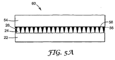
図5Aは、図4の方法によって製造されたスクリーンの一実施形態の側面図である。大きい厚さまたは量の光吸収接着剤56が使用される場合、図4の工程は、完全に充填された構造60をもたらす。1つの例示的な実施形態において、光吸収接着剤56は、完全に充填された構造60内で効率的なTIRを生じさせるために低屈折率を有する。光吸収接着剤56は、拡散体リブ24をシールド54に効果的に接合するように配合される。光吸収接着剤56は、見かけ上受入れられる積層結果を生じさせるために、低収縮特性を所有することができる。さらに、好都合な処理および速い硬化を考慮するために、光吸収接着剤56が紫外光によって硬化可能であることが特に適している。
FIG. 5A is a side view of one embodiment of a screen manufactured by the method of FIG. If a large thickness or amount of
一実施形態において、光拡散リブ24は、図2の微細複製プロセス28に示されているように、高屈折率拡散体樹脂を使用するツーリングモールドから複製される。本出願において、特に明記しない限り、すべてのパーセンテージは質量による。1つの適切な樹脂は、約79%の脂肪族ウレタンアクリレートオリゴマーおよび約19%の2−フェノキシエチルアクリレート、および約2%の2−ヒドロキシ−2−メチル−1−フェニル−1−プロパノン光開始剤である。別の適切な樹脂は、約69%の脂肪族ウレタンアクリレートオリゴマー、約29%の2−(1−ナフチルオキシ)−エチルアクリレート、および約2%の2−ヒドロキシ−2−メチル−1−フェニル−1−プロパノン光開始剤である。リブ24を形成するための樹脂は、樹脂コーティングステーション32から基板またはベース構造22上にコーティングされる。上に樹脂を有するベース構造22は、微細構造化シリンダ36によって成形され、紫外線(UV)ランプまたは電子ビーム38によって硬化される。典型的なUV硬化条件は、1分あたり約10フィート(3.05m)から約20フィート(6.10m)のベルト速度で動作される600ワット/in(23.62W/mm)フュージョン・システムズバルブシステムを使用し、UVバルブの下の1つ以上の通過を伴う。形成されたマイクロリブ構造20は微細複製プロセス28から取出され、自立構造をもたらす。
In one embodiment, the
次に、着色された、典型的には黒色の光吸収接着剤56が、シールド54などの第2の基板に塗布される。1つの適切な光吸収接着剤56は、約30%のA配合物A”(A配合物Aは、約38.5%の脂肪族ウレタンアクリレートオリゴマーと、約26.9%のエトキシエトキシエチルアクリレートと、約28.8%のイソボルニルアクリレートと、約5.8%のヘキサンジオールジアクリレートと、約1%未満のα,α−ジエトキシアセトフェンケ(diethoxyacetophenche)(DEAP)光開始剤とを有する)と;約10%の脂肪族ウレタンジアクリレートと;約30%のトリフルオロエチルアクリレートと;約30%のN−メチル−ペルフルオロブチルスルホンアミドエチルアクリレートとを有する樹脂から形成される。別の適切な光吸収材料56は、約50%の上で説明されたA配合物Aと、約50%のN−メチル−ペルフルオロブチルスルホンアミドエチルアクリレートとを有する樹脂から形成される。1つの例示的な実施形態において、光吸収接着剤56は、カーボンブラックなどの顔料を含有する。1つの例示的な実施形態において、顔料は約50ppm(百万分率)から約20,000ppmの濃度で使用される。1つの例示的な実施形態において、顔料は約1,000ppmを超え、かつ約9,000ppm未満の濃度で使用される。カーボンブラック材料と接着剤材料との質量比に基いて、約3,000ppmの濃度が特に適している。
Next, a colored, typically black, light absorbing
光吸収接着剤56は、十分な量でシールド54などの第2の基板に塗布されて、図4に示された積層方法において、拡散体リブ24を完全に充填し、わずかな余分を可能にして、完全な充填を確実にする。余分な接着剤は、積層されると、完全に充填された構造60から圧搾される。次に、完全に充填された構造60は、微細複製プロセス28について上で説明された条件と同様の条件下で放射線に曝される。照射は、たとえば、材料の部分的なまたは完全な重合をもたらすことができる。少なくとも部分的な重合の後、光吸収接着剤56はその成分のコポリマーである。
図5Bは、図4の方法によって製造されたスクリーンの第2の実施形態の側面図である。小さい厚さまたは量の光吸収接着剤56が、図4に示された工程で使用される場合、部分的に充填された構造64が生じる。部分的に充填された構造64において、空気間隙66がV字形溝26内に残される。空気間隙66の利益は、低屈折率の空気がリブ溝26を充填し、溝26と光拡散リブ24との間の大きい屈折率差を生じさせ、ATIR効率@をさらに向上させることである。空気の屈折率が1.0であるので、空気間隙66と光拡散リブ24との間の屈折率の差は、通常、約0.5を超える。空気間隙66が拡散体リブ界面のバルクを作るので、光吸収接着剤56は、構造60においてリブが完全に充填される場合と同じほど低い屈折率を所有する必要はない。これは、たとえば低収縮および高剥離強度接着などの、他の重要な特性を最適化するための接着剤56の選択を考慮する。光吸収接着剤56と拡散体リブ24との間の接着剤接触領域がより小さいので、光吸収接着剤56は、部分的に充填された構造64において、完全に充填された構造60より大きい接着剤特性を所有しなければならない。
FIG. 5B is a side view of a second embodiment of a screen manufactured by the method of FIG. When a small thickness or amount of
完全に充填された構造60および部分的に充填された構造64の両方において、光吸収接着剤56に使用される光吸収材料のレベルは、コントラスト向上および周囲光吸収の所望の量に基いて選択される。例示的な実施形態における光吸収材料は、カーボンブラックなどの黒色顔料である。完全に充填された構造60において、黒色顔料濃度は、比較的低いことができるが、受入れられる全体的な一定の吸光度(absorbence)または光学密度値をもたらすことができ、というのは、光吸収接着剤56の層の厚さが大きいからである。一実施形態における、完全に充填された構造60内の、カーボンブラックなどの顔料の適切なローディング濃度は、約50ppmから約20,000ppmである。例示的な実施形態において、濃度は約1000ppm(百万分率)を超え、かつ約9000ppm未満である。カーボンブラック材料と接着剤材料との質量比に基いて、約3000ppmの濃度が特に適している。しかし、部分的に充填された構造64において、コーティング厚さは小さく、したがって、黒色顔料濃度は、同じ光学密度をもたらすためにより大きくなければならない。後者の場合、周囲光吸収は、前者の場合より、コーティング厚さの単位あたり大きい。一実施形態における、部分的に充填された構造64内の、カーボンブラックなどの顔料の適切なローディング濃度は、約50ppmから約20,000ppmである。例示的な実施形態において、濃度は、カーボンブラック材料と接着剤材料との質量比に基いて、約5,000ppmを超え、かつ約10,000ppm未満である。
In both the fully filled
完全に充填された構造60および部分的に充填された構造64の両方における課題は、積層の間の、拡散体リブ24の前面50からの余分な接着剤56の除去である。積層の間、光吸収接着剤56のすべてが拡散体リブ24の前面50から除去されない場合、TIR透過の間、いくらかの画像光が失われることがある。より高度に着色された接着剤56を有する部分的に充填された構造64において、画像光のより多い損失が、同じ残留黒色層厚さについて生じる。
The challenge in both the fully filled
図6は、さまざまな黒色接着剤配合物に基いたスクリーン性能を示すグラフである。スクリーン性能を測定する1つの方法は、視野角の関数としての水平ゲイン曲線をプロットすることによる。プロットされた曲線は、見る人がスクリーンの中心から離れて横に移動するとき、見る人によって認められるスクリーンの輝度を説明する。ATIR効率は、全内部反射をもたらす入射光角度の範囲に関連し、範囲が大きいほど、効率が高い。TIR効率およびRI差の両方が増加するにつれて、ゲイン曲線のピーク(ほぼ30度の水平ビューイング)が最大に上昇する。リブ24側面からの反射は、示されているようなゲイン曲線の局所的な最大値をもたらすことができる。局所的な最大値の影響を、たとえば、光拡散をプロジェクションスクリーンに導入することによって、低減するかなくすことができる。たとえば、リブ24は、入射光を散乱させることによって局所的な最大値をより顕著でないようにするために粒子を含むことができる。
FIG. 6 is a graph showing screen performance based on various black adhesive formulations. One way to measure screen performance is by plotting a horizontal gain curve as a function of viewing angle. The plotted curve explains the screen brightness as seen by the viewer as the viewer moves sideways away from the center of the screen. ATIR efficiency is related to the range of incident light angles that result in total internal reflection, the greater the range, the higher the efficiency. As both TIR efficiency and RI difference increase, the peak of the gain curve (approximately 30 degrees horizontal viewing) rises to the maximum. Reflection from the
曲線68が、キャビティ26を光吸収材料で充填するための標準平面化技術を用いるベンチマーク標準スクリーンを指す。ベンチマーク標準スクリーンは、約80%の脂肪族ウレタンアクリレートオリゴマーと、約20%の2−フェノキシエチルアクリレートとを有する樹脂から形成された光拡散リブ24を有する。光拡散リブ24の屈折率は約1.51である。光吸収材料46は、約60%のゴールドシュミット・コーポレーション(Goldschmidt Corp.)からの所有権を持つ(proprietary)RC709シリコーンアクリレートと、約39%のプロポキシル化(propoxylated)ネオペンチルグリコールジアクリレートと、約1%のダロキュア(Darocur)4275(2−ヒドロキシ−2−メチル−1−フェニル−1−プロパノンおよびジフェニル(2,4,6−トリメチルベンゾイル)−ホスフィンオキシドの1:1ブレンド)光開始剤とを有し、約3,000ppmの濃度のカーボンブラック顔料を有する樹脂から形成される。光吸収材料46の屈折率は約1.45である。光吸収材料46と光拡散リブ24との間のRI差は約0.06である。光吸収材料46のこの配合物は、低収縮特徴、良好な処理特性、黒色顔料の均一な分散、低価格、および広範囲に及ぶ入手可能性を所有する。
曲線70が、図4および図5Aに示された方法によって形成されたスクリーンを指し、これは、拡散体リブ24と光吸収接着剤56との間のRI差が約0.01未満である場合のゲインを示す。曲線70に対応するスクリーンは、約80%の脂肪族ウレタンアクリレートオリゴマーと、約20%の2−フェノキシエチルアクリレートとを有する樹脂から形成された光拡散リブ24を有する。光拡散リブ24の屈折率は約1.51である。光吸収材料56は、約38.5%の脂肪族ウレタンアクリレートオリゴマーと、約26.9%のエトキシエトキシエチルアクリエート(ethoxyethoxyethyl acryate)と、約28.8%のイソボルニルアクリレートと、約5.8%のヘキサンジオールジアクリエート(hexanediol diacryate)と、約1%未満のα,α−ジエトキシアセトフェノン(DEAP)光開始剤とを有するA配合物A”樹脂から形成される。光吸収材料56の屈折率は約1.50である。
曲線72が、図4および図5Aに示された方法によって形成されたスクリーンを指し、これは、比較的低いRIを有する光吸収接着剤56が使用される場合の増加されたATIR効率を有する。曲線72に対応するスクリーンは、約80%の脂肪族ウレタンアクリレートオリゴマーと、約20%の2−フェノキシエチルアクリレートとを有する樹脂から形成された光拡散リブ24を有する。光拡散リブ24の屈折率は約1.51である。光吸収材料56は、約30%の上で説明されたA配合物Aと、約10%の脂肪族ウレタンジアクリレートと、約30%のトリフルオロエチルアクリレートと、約30%のN−メチル−ペルフルオロブチルスルホンアミドエチルアクリレートと、約1%未満のα,α−ジエトキシアセトフェノン(DEAP)光開始剤とを有する樹脂から形成される。光吸収接着剤56の屈折率は約1.44である。
最後に、曲線74が、図4および図5Aに示された方法によって形成されたスクリーンを指し、TIR効率は増加され、光吸収接着剤56と光拡散リブ24との間のRI差は約0.08である。曲線74に対応するスクリーンは、約70%の脂肪族ウレタンアクリレートオリゴマーと、約30%の2−(1−ナフチルオキシ)−エチルアクリレートとを有する樹脂から形成された光拡散リブ24を有する。光拡散リブ24の屈折率は約1.5338である。光吸収材料46は、約50%の上で説明されたA配合物Aと、約50%のN−メチル−ペルフルオロブチルスルホンアミドエチルアクリレートと、約1%未満のα,α−ジエトキシアセトフェノン(DEAP)光開始剤とを有する樹脂から形成される。光吸収材料56の屈折率は約1.45である。
Finally,
図6に示されているように、光拡散リブ24の配合物に対する光吸収接着剤56の配合物は、所望のスクリーン性能特徴をもたらすように選択することができる。通常、配合物は、光吸収接着剤56と光拡散リブ24との間のRI差を最大にするように選択される。光拡散リブ24および保護シールド54への強い接着を行い、比較的低いRIを所有し、硬化後の高い機械的強度、ならびに適切な粘度および紫外光による硬化性などの処理可能性特性を有することが、光吸収接着剤56には望ましい。光吸収材料56の適切な成分は脂肪族ウレタンアクリレートオリゴマーである。いくつかの実施形態において、光吸収接着剤56は、脂肪族ウレタンアクリレートオリゴマー少なくとも約5パーセントを含有する。例示的な実施形態において、光吸収接着剤56は、脂肪族ウレタンアクリレートオリゴマー少なくとも約10パーセントを含有する。いくつかの実施形態において、光吸収接着剤56は、脂肪族ウレタンアクリレートオリゴマー約50パーセント未満を含有する。例示的な実施形態において、光吸収接着剤56は、脂肪族ウレタンアクリレートオリゴマー約40パーセント未満を含有する。脂肪族ウレタンアクリレートオリゴマーの濃度が低すぎる場合、光吸収接着剤56は十分粘性でないことがあり、濃度が高すぎる場合、光吸収接着剤56は粘性すぎることがあり、屈折率は高すぎることがある。
As shown in FIG. 6, the formulation of
光吸収接着剤56の別の適切な成分は低RI相溶性アクリレートモノマーであり、そのうち、エトキシエトキシエチルアクリレートが一例である。いくつかの実施形態において、光吸収接着剤56は、アクリレートモノマー少なくとも約1パーセントを含有する。例示的な実施形態において、光吸収接着剤56は、アクリレートモノマー少なくとも約8パーセントを含有する。いくつかの実施形態において、光吸収接着剤56は、アクリレートモノマー約30パーセント未満を含有する。例示的な実施形態において、光吸収接着剤56は、アクリレートモノマー約20パーセント未満を含有する。例示的な(exemplory)実施形態において、アクリレートモノマーは、低RIを有し、かつ光吸収接着剤56の他の成分の相溶性を向上させるための溶媒として役立つ。
Another suitable component of light absorbing
光吸収材料56の別の適切な成分は、強度を加えるための多官能性アクリレートモノマーであり、そのうち、ヘキサンジオールジアクリレートが一例である。いくつかの実施形態において、光吸収接着剤56は、多官能性アクリレートモノマー少なくとも約0.1パーセントを含有する。例示的な実施形態において、光吸収接着剤56は、多官能性アクリレートモノマー少なくとも約1.0パーセントを含有する。いくつかの実施形態において、光吸収接着剤56は、多官能性アクリレートモノマー約10パーセント未満を含有する。例示的な実施形態において、光吸収接着剤56は、多官能性アクリレートモノマー約6パーセント未満を含有する。多官能性アクリレートモノマーの機能性が高いほど、必要な濃度が低い。
Another suitable component of the
曲線70によって示された、A配合物A光吸収接着剤56を有するスクリーンは、光学性能を最適にするには高すぎるRIを有する。光吸収接着剤56のRIを減少させるための1つの相溶性成分は、ペルフルオロアルキルスルホンアミドエチルアクリレートであり、そのうち、N−メチル−ペルフルオロブチルスルホンアミドエチルアクリレートが一例である。ペルフルオロアルキルスルホンアミドエチルアクリレートは、光吸収接着剤56の接着特性を向上させる。いくつかの実施形態において、光吸収接着剤56は、ペルフルオロアルキルスルホンアミドエチルアクリレート少なくとも約1パーセントを含有する。例示的な実施形態において、光吸収接着剤56は、ペルフルオロアルキルスルホンアミドエチルアクリレート少なくとも約10パーセントを含有する。いくつかの実施形態において、光吸収接着剤56は、ペルフルオロアルキルスルホンアミドエチルアクリレート約70パーセント未満を含有する。例示的な実施形態において、光吸収接着剤56は、ペルフルオロアルキルスルホンアミドエチルアクリレート約50パーセント未満を含有する。
The screen shown by
光吸収材料56が光重合される場合、適切な光開始剤が含まれ、フェニルビス(2,4,6トリメチルベンゾイル)ホスフィンオキシド光開始剤およびα,α−ジエトキシアセトフェノン(DEAP)光開始剤が、適切なフリーラジカル光開始剤の例である。いくつかの実施形態において、光吸収接着剤56は、光開始剤少なくとも約0.5パーセントを含有する。例示的な実施形態において、光吸収接着剤56は、光開始剤約1.0パーセントを含有する。いくつかの実施形態において、光吸収接着剤56は、光開始剤約5パーセント未満を含有する。他の実施形態において、熱重合開始剤またはレドックス開始剤が選択される。
When the
本発明を例示的な実施形態に関して説明したが、当業者は、本発明の精神および範囲から逸脱することなく形態および詳細に変更を行うことができることを認めるであろう。たとえば、光拡散構造および光吸収構造の特定の形状を示したが、構造を、付加的なまたは異なった平面または角度、付加的な端縁、および湾曲した表面を組入れ、異なった形状で形成することができることが企図される。たとえば、特定の基板上の光拡散構造がすべて同じ高さまたは形状である必要はないことがさらに認められる。同様に、たとえば、特定の基板上の光吸収構造がすべて同じ高さまたは形状である必要はない。さらに、そこで説明された材料およびプロセスの構成要素は多数の方法で組合せ可能であり、それらの可能性の少しだけを例として具体的に説明したが、すべてが本発明の範囲内であるとみなされる。 Although the present invention has been described in terms of exemplary embodiments, those skilled in the art will recognize that changes may be made in form and detail without departing from the spirit and scope of the invention. For example, although particular shapes of light diffusing structures and light absorbing structures have been shown, the structures can be formed in different shapes, incorporating additional or different planes or angles, additional edges, and curved surfaces. It is contemplated that it can be. For example, it is further appreciated that the light diffusing structures on a particular substrate need not all be the same height or shape. Similarly, for example, the light absorbing structures on a particular substrate need not all be the same height or shape. Furthermore, the materials and process components described therein can be combined in a number of ways, and only a few of those possibilities have been specifically described by way of example, but all are considered to be within the scope of the present invention. It is.
20 マイクロリブ構造
22 ベース構造
23 ベース
24 光拡散リブ
25 壁
26 V字形溝
28 微細複製プロセス
30 基板巻出しステーション
32 樹脂コーティングステーション
34 精密ニップロール
36 微細構造化シリンダ
38 紫外線ランプ
40 精密ニップロール
42 フィルムリワインド
44 埋込まれた微細構造化フィルム
46 光吸収材料
48 内部反射表面
50 前面
52 光学透過領域
54 シールド
56 光吸収接着剤
58 54の背面
59 矢印
60 完全に充填された構造
62 22の背面
64 部分的に充填された構造
66 空気間隙
68 曲線:651/530
70 曲線:651/PO−1
72 曲線:651/953
74 曲線:651/945
20
70 curve: 651 / PO-1
72 Curve: 651/953
74 Curve: 651/945
Claims (23)
互いに反対側の第1および第2の主表面を有する第1の光透過基板、ならびに前記第1の表面上に配置された複数の光拡散構造を提供する工程であって、前記構造がそれらの間の複数のキャビティを規定する工程と、
互いに反対側の第1および第2の主表面を有する第2の基板、ならびに前記第2の基板の第1の表面上に配置された光吸収材料を提供する工程と、
前記第1の基板の第1の表面を前記第2の基板の第1の表面に隣接して位置決めして、前記光吸収材料で前記キャビティを少なくとも部分的に充填する工程と、
を含む方法。 A method for forming a light dispersion film, comprising:
Providing a first light transmissive substrate having first and second major surfaces opposite to each other, and a plurality of light diffusing structures disposed on the first surface, wherein the structures are those Defining a plurality of cavities between,
Providing a second substrate having first and second major surfaces opposite to each other, and a light absorbing material disposed on the first surface of the second substrate;
Positioning the first surface of the first substrate adjacent to the first surface of the second substrate and at least partially filling the cavity with the light absorbing material;
Including methods.
前記基板上に配置された複数の光拡散構造であって、それらの間の複数のキャビティを規定する複数の光拡散構造と、
前記キャビティを少なくとも部分的に充填する光吸収接着剤と、
を含むスクリーン用光分散フィルム。 A light transmissive substrate;
A plurality of light diffusing structures disposed on the substrate, the plurality of light diffusing structures defining a plurality of cavities therebetween;
A light absorbing adhesive that at least partially fills the cavity;
A light dispersion film for a screen comprising
上に複数の光拡散構造が配置された光透過基板を提供する工程であって、前記構造が、それらの間の複数のキャビティを規定する工程と、
光吸収接着剤で前記キャビティを少なくとも部分的に充填する工程と、
を含む方法。 A method for forming a light dispersion film, comprising:
Providing a light transmissive substrate having a plurality of light diffusing structures disposed thereon, the structure defining a plurality of cavities therebetween;
At least partially filling the cavity with a light absorbing adhesive;
Including methods.
Applications Claiming Priority (2)
| Application Number | Priority Date | Filing Date | Title |
|---|---|---|---|
| US10/733,066 US7057810B2 (en) | 2003-12-11 | 2003-12-11 | Microstructured screen with light absorbing material and method of manufacturing |
| PCT/US2004/040199 WO2005062118A1 (en) | 2003-12-11 | 2004-12-01 | Microstructured screen with light absorbing material and method of manufacturing |
Publications (2)
| Publication Number | Publication Date |
|---|---|
| JP2007514202A true JP2007514202A (en) | 2007-05-31 |
| JP2007514202A5 JP2007514202A5 (en) | 2008-01-24 |
Family
ID=34653011
Family Applications (1)
| Application Number | Title | Priority Date | Filing Date |
|---|---|---|---|
| JP2006543880A Withdrawn JP2007514202A (en) | 2003-12-11 | 2004-12-01 | Microstructured screen with light-absorbing material and manufacturing method |
Country Status (7)
| Country | Link |
|---|---|
| US (2) | US7057810B2 (en) |
| EP (1) | EP1692568A1 (en) |
| JP (1) | JP2007514202A (en) |
| CN (1) | CN1890601A (en) |
| MX (1) | MXPA06006366A (en) |
| TW (1) | TW200530741A (en) |
| WO (1) | WO2005062118A1 (en) |
Cited By (8)
| Publication number | Priority date | Publication date | Assignee | Title |
|---|---|---|---|---|
| WO2009034992A1 (en) * | 2007-09-12 | 2009-03-19 | Dai Nippon Printing Co., Ltd. | Optical sheet, display device and optical sheet manufacturing method |
| JP2009237113A (en) * | 2008-03-26 | 2009-10-15 | Dainippon Printing Co Ltd | Optical sheet and display device |
| WO2011068168A1 (en) * | 2009-12-03 | 2011-06-09 | シャープ株式会社 | Light diffusion sheet, method for manufacturing same, and transmissive display device provided with light diffusion sheet |
| JP2011252939A (en) * | 2010-05-31 | 2011-12-15 | Dainippon Printing Co Ltd | Manufacturing method of visibility improvement sheet, and visibility improvement sheet |
| WO2012053501A1 (en) * | 2010-10-21 | 2012-04-26 | シャープ株式会社 | Light-diffusion member, manufacturing method thereof, and display device |
| JP2013137571A (en) * | 2013-03-14 | 2013-07-11 | Dainippon Printing Co Ltd | Method for manufacturing optical sheet |
| WO2014084261A1 (en) * | 2012-11-30 | 2014-06-05 | シャープ株式会社 | Light control film and display device |
| JP2016167079A (en) * | 2011-12-27 | 2016-09-15 | シャープ株式会社 | Liquid crystal display, light control film, and display |
Families Citing this family (27)
| Publication number | Priority date | Publication date | Assignee | Title |
|---|---|---|---|---|
| DE10325437A1 (en) * | 2003-06-05 | 2004-12-23 | Bayer Materialscience Ag | Polycarbonate molded body with low Staubanziehung |
| US20050127541A1 (en) * | 2003-12-11 | 2005-06-16 | 3M Innovative Properties Company | Microstructured screen and method of manufacturing using coextrusion |
| US7057810B2 (en) * | 2003-12-11 | 2006-06-06 | 3M Innovative Properties Company | Microstructured screen with light absorbing material and method of manufacturing |
| WO2005116740A1 (en) * | 2004-05-31 | 2005-12-08 | Sekonix Co., Ltd. | Optical device for a display having tapered waveguide and process for making the same |
| JP2011501219A (en) | 2007-10-16 | 2011-01-06 | スリーエム イノベイティブ プロパティズ カンパニー | Higher transmittance light control film |
| EP2235570A4 (en) * | 2007-12-21 | 2014-10-15 | 3M Innovative Properties Co | Light control film |
| KR101714807B1 (en) | 2009-06-18 | 2017-03-09 | 쓰리엠 이노베이티브 프로퍼티즈 컴파니 | Light control film |
| KR101137390B1 (en) * | 2009-12-24 | 2012-04-26 | 삼성모바일디스플레이주식회사 | Optical film and organic light emitting display apparatus having the same |
| GB201016566D0 (en) | 2010-10-01 | 2010-11-17 | Barco Nv | Curved back projection screen |
| US8562145B2 (en) | 2011-06-22 | 2013-10-22 | 3M Innovative Properties Company | Display system and method for projection onto non-planar surfaces |
| JP6239978B2 (en) * | 2011-10-28 | 2017-11-29 | シャープ株式会社 | Liquid crystal display |
| US10067379B2 (en) * | 2012-04-02 | 2018-09-04 | Sharp Kabushiki Kaisha | Liquid crystal display device |
| US8599483B1 (en) | 2012-06-05 | 2013-12-03 | 3M Innovative Properties Company | High angle rear projection system |
| US9709841B2 (en) * | 2012-08-10 | 2017-07-18 | Sharp Kabushiki Kaisha | Liquid crystal display device |
| JP6194581B2 (en) * | 2012-12-12 | 2017-09-13 | 大日本印刷株式会社 | Transparent screen and video display device |
| JP6480407B2 (en) | 2013-03-13 | 2019-03-13 | スリーエム イノベイティブ プロパティズ カンパニー | Electronically switchable privacy device |
| JP6351217B2 (en) * | 2013-07-05 | 2018-07-04 | シャープ株式会社 | Light diffusing member manufacturing equipment |
| CN107367898B (en) * | 2016-05-12 | 2019-05-03 | 深圳光峰科技股份有限公司 | A kind of production method and dependent projections screen of projection screen |
| US20180120580A1 (en) | 2016-10-28 | 2018-05-03 | 3M Innovative Properties Company | Light control film with varied viewing angle |
| US10288995B2 (en) | 2017-06-15 | 2019-05-14 | Esterline Belgium Bvba | Aspherical dome display and method of rear projection |
| CN110083005A (en) * | 2018-01-23 | 2019-08-02 | 台湾扬昕股份有限公司 | Rear projection screen |
| CN208110256U (en) * | 2018-03-21 | 2018-11-16 | 中强光电股份有限公司 | Back projection curtain |
| CN111269604B (en) * | 2018-12-03 | 2022-01-04 | 深圳光峰科技股份有限公司 | Projection screen combined coating and preparation method of projection screen |
| CN110576623B (en) * | 2019-09-17 | 2021-12-07 | 成都市冠宇复合材料制品有限公司 | Production process of high-precision large glass fiber reinforced plastic projection screen shell substrate and shell manufactured by production process |
| CN114846369B (en) * | 2019-12-23 | 2024-10-25 | 3M创新有限公司 | High transmittance light control film |
| CN111290211A (en) * | 2020-03-31 | 2020-06-16 | 深圳市真屏科技发展有限公司 | Transparent projection film |
| US20240142674A1 (en) * | 2021-01-19 | 2024-05-02 | 3M Innovative Properties Company | Article and method of manufacture thereof |
Family Cites Families (30)
| Publication number | Priority date | Publication date | Assignee | Title |
|---|---|---|---|---|
| US27886A (en) * | 1860-04-17 | Fireplace | ||
| US265602A (en) * | 1882-10-10 | hergenroedee | ||
| US139549A (en) * | 1873-06-03 | Improvement in compound steam-engines | ||
| US139550A (en) * | 1873-06-03 | Improvement in compound hose-pipes | ||
| JPS5780025A (en) | 1980-11-05 | 1982-05-19 | Toowa:Kk | Continuous manufacture of synthetic resin lace patterned material |
| US4701019A (en) | 1986-12-05 | 1987-10-20 | North American Philips Corporation | Selective application of light-absorbing particles to a lenticular screen |
| US5126189A (en) | 1987-04-21 | 1992-06-30 | Gelman Sciences, Inc. | Hydrophobic microporous membrane |
| US5128387A (en) | 1987-07-28 | 1992-07-07 | Borden, Inc. | Extensible and pasteurizable radiation curable coating for metal |
| US5104929A (en) | 1988-04-11 | 1992-04-14 | Minnesota Mining And Manufacturing Company | Abrasion resistant coatings comprising silicon dioxide dispersions |
| JPH0478841A (en) | 1990-07-23 | 1992-03-12 | Asahi Chem Ind Co Ltd | High-resolution transmission type screen |
| EP0484073B1 (en) | 1990-10-29 | 2000-04-05 | Kuraray Co., Ltd. | Lenticular lens sheet |
| JP3158476B2 (en) | 1991-03-28 | 2001-04-23 | 凸版印刷株式会社 | Method for manufacturing double-sided lenticular sheet |
| JP2705358B2 (en) | 1991-05-28 | 1998-01-28 | 凸版印刷株式会社 | Method of manufacturing transmission projection screen |
| US5270378A (en) | 1992-10-26 | 1993-12-14 | Minnesota Mining And Manufacturing Company | Acrylic surfactants and compositions containing those surfactants |
| US5481385A (en) * | 1993-07-01 | 1996-01-02 | Alliedsignal Inc. | Direct view display device with array of tapered waveguide on viewer side |
| US5462700A (en) | 1993-11-08 | 1995-10-31 | Alliedsignal Inc. | Process for making an array of tapered photopolymerized waveguides |
| US5521726A (en) * | 1994-08-26 | 1996-05-28 | Alliedsignal Inc. | Polarizer with an array of tapered waveguides |
| WO1996009154A1 (en) | 1994-09-23 | 1996-03-28 | Karszes William M | Method of making lenticular plastics |
| US5609990A (en) | 1995-02-08 | 1997-03-11 | Imation Corp. | Optical recording disk having a sealcoat layer |
| US5633049A (en) | 1995-04-20 | 1997-05-27 | Minnesota Mining And Manufacturing Company | Method of making protective coating for thermoplastic transparencies |
| JP3816137B2 (en) | 1996-02-06 | 2006-08-30 | 旭化成ケミカルズ株式会社 | Method for producing polycarbonate sheet |
| US5822489A (en) | 1996-12-31 | 1998-10-13 | Lucent Technologies, Inc. | Low refractive index photo-curable composition for waveguide applications |
| US6417966B1 (en) | 1999-07-07 | 2002-07-09 | 3M Innovative Properties Company | Rear projection screen using internal reflection |
| WO2001030873A1 (en) | 1999-10-27 | 2001-05-03 | 3M Innovative Properties Company | Fluorochemical sulfonamide surfactants |
| US6821178B2 (en) | 2000-06-08 | 2004-11-23 | 3M Innovative Properties Company | Method of producing barrier ribs for plasma display panel substrates |
| US6636355B2 (en) | 2000-12-27 | 2003-10-21 | 3M Innovative Properties Company | Microstructured rear projection screen |
| US6559198B2 (en) | 2001-07-05 | 2003-05-06 | Nick Novicky | Fluorocarbon-sulfone hydrophilic contact lenses, optical medical devices and compositions thereof |
| US7534500B2 (en) | 2001-10-05 | 2009-05-19 | Bridgestone Corporation | Transparent electroconductive film, method for manufacture thereof, and touch panel |
| CN1639629A (en) | 2002-03-08 | 2005-07-13 | 优泊公司 | Screen |
| US7057810B2 (en) * | 2003-12-11 | 2006-06-06 | 3M Innovative Properties Company | Microstructured screen with light absorbing material and method of manufacturing |
-
2003
- 2003-12-11 US US10/733,066 patent/US7057810B2/en not_active Expired - Fee Related
-
2004
- 2004-12-01 EP EP04812658A patent/EP1692568A1/en not_active Withdrawn
- 2004-12-01 WO PCT/US2004/040199 patent/WO2005062118A1/en active Application Filing
- 2004-12-01 JP JP2006543880A patent/JP2007514202A/en not_active Withdrawn
- 2004-12-01 CN CNA2004800367072A patent/CN1890601A/en active Pending
- 2004-12-01 MX MXPA06006366A patent/MXPA06006366A/en unknown
- 2004-12-10 TW TW093138442A patent/TW200530741A/en unknown
-
2006
- 2006-03-23 US US11/387,539 patent/US7184210B2/en not_active Expired - Fee Related
Cited By (14)
| Publication number | Priority date | Publication date | Assignee | Title |
|---|---|---|---|---|
| US8888303B2 (en) | 2007-09-12 | 2014-11-18 | Dai Nippon Printing Co., Ltd. | Optical sheet controlling external light, display device and method for producing optical sheet |
| JP2009069416A (en) * | 2007-09-12 | 2009-04-02 | Dainippon Printing Co Ltd | Optical sheet, display device, and manufacturing method of optical sheet |
| WO2009034992A1 (en) * | 2007-09-12 | 2009-03-19 | Dai Nippon Printing Co., Ltd. | Optical sheet, display device and optical sheet manufacturing method |
| KR101490542B1 (en) * | 2007-09-12 | 2015-02-05 | 다이니폰 인사츠 가부시키가이샤 | Optical sheet, display device and optical sheet manufacturing method |
| JP2009237113A (en) * | 2008-03-26 | 2009-10-15 | Dainippon Printing Co Ltd | Optical sheet and display device |
| WO2011068168A1 (en) * | 2009-12-03 | 2011-06-09 | シャープ株式会社 | Light diffusion sheet, method for manufacturing same, and transmissive display device provided with light diffusion sheet |
| JP2011252939A (en) * | 2010-05-31 | 2011-12-15 | Dainippon Printing Co Ltd | Manufacturing method of visibility improvement sheet, and visibility improvement sheet |
| WO2012053501A1 (en) * | 2010-10-21 | 2012-04-26 | シャープ株式会社 | Light-diffusion member, manufacturing method thereof, and display device |
| US9274255B2 (en) | 2010-10-21 | 2016-03-01 | Sharp Kabushiki Kaisha | Light-diffusion member, manufacturing method thereof, and display device |
| JP2016167079A (en) * | 2011-12-27 | 2016-09-15 | シャープ株式会社 | Liquid crystal display, light control film, and display |
| WO2014084261A1 (en) * | 2012-11-30 | 2014-06-05 | シャープ株式会社 | Light control film and display device |
| JP2014109625A (en) * | 2012-11-30 | 2014-06-12 | Sharp Corp | Light-controlling film and display device |
| US9541787B2 (en) | 2012-11-30 | 2017-01-10 | Sharp Kabushiki Kaisha | Light control film including light control layer with reflection surface and display device including same |
| JP2013137571A (en) * | 2013-03-14 | 2013-07-11 | Dainippon Printing Co Ltd | Method for manufacturing optical sheet |
Also Published As
| Publication number | Publication date |
|---|---|
| US7057810B2 (en) | 2006-06-06 |
| US20060158724A1 (en) | 2006-07-20 |
| WO2005062118A1 (en) | 2005-07-07 |
| TW200530741A (en) | 2005-09-16 |
| US20050128579A1 (en) | 2005-06-16 |
| EP1692568A1 (en) | 2006-08-23 |
| US7184210B2 (en) | 2007-02-27 |
| CN1890601A (en) | 2007-01-03 |
| MXPA06006366A (en) | 2006-08-23 |
Similar Documents
| Publication | Publication Date | Title |
|---|---|---|
| US7184210B2 (en) | Microstructured screen with light absorbing material and method of manufacturing | |
| EP1692551B1 (en) | Composition for microstructured screens | |
| US20050127541A1 (en) | Microstructured screen and method of manufacturing using coextrusion | |
| JP6064984B2 (en) | Light control sheet and liquid crystal display device using the light control sheet | |
| TWI385468B (en) | A light diffusion member, a transmissive type screen, a rear projection type display device, and a light absorbing portion forming resin composition | |
| JP5573394B2 (en) | Optical sheet manufacturing method, optical sheet, and image display device | |
| KR101356903B1 (en) | Optical film | |
| KR20090088438A (en) | Lens sheet, surface light source device and liquid crystal display device | |
| KR20130041215A (en) | Light-scattering film, method of manufacturing same, light-scattering polarizing plate, and liquid-crystal display device | |
| JP2006163263A (en) | Transmission type screen | |
| JP4968728B2 (en) | Light control film laminate for projection screen, method for manufacturing the same, and projection screen | |
| JP2007225972A (en) | Light diffusion film, optical member, rear projection screen and rear projection display device | |
| JP2005283749A (en) | Optical diffusion film, its manufacturing method, and screen | |
| WO2005088356A1 (en) | Transmitting screen-use light diffusing member | |
| CN100523872C (en) | Transparent film and method for manufacturing the same, polarized plate and image display device | |
| KR20070110173A (en) | Projection screen | |
| JP2005234088A (en) | Light diffusion film, its manufacturing method, and screen | |
| JP4258400B2 (en) | Lens sheet and transmissive screen | |
| JP5740856B2 (en) | Optical sheet, optical sheet manufacturing method, and image display device | |
| JP2010069839A (en) | Hard coat film and method of manufacturing the same | |
| JP2015184322A (en) | Light control sheet, image source unit, and method of manufacturing light control sheet | |
| JP2014071148A (en) | Optical sheet, surface light source device, and liquid crystal display device |
Legal Events
| Date | Code | Title | Description |
|---|---|---|---|
| A521 | Request for written amendment filed |
Free format text: JAPANESE INTERMEDIATE CODE: A523 Effective date: 20071129 |
|
| A621 | Written request for application examination |
Free format text: JAPANESE INTERMEDIATE CODE: A621 Effective date: 20071129 |
|
| A761 | Written withdrawal of application |
Free format text: JAPANESE INTERMEDIATE CODE: A761 Effective date: 20080606 |