JP2007508731A - Power conversion system - Google Patents
Power conversion system Download PDFInfo
- Publication number
- JP2007508731A JP2007508731A JP2006530749A JP2006530749A JP2007508731A JP 2007508731 A JP2007508731 A JP 2007508731A JP 2006530749 A JP2006530749 A JP 2006530749A JP 2006530749 A JP2006530749 A JP 2006530749A JP 2007508731 A JP2007508731 A JP 2007508731A
- Authority
- JP
- Japan
- Prior art keywords
- power conversion
- pulse
- voltage
- conversion system
- pma
- Prior art date
- Legal status (The legal status is an assumption and is not a legal conclusion. Google has not performed a legal analysis and makes no representation as to the accuracy of the status listed.)
- Abandoned
Links
Images


Classifications
-
- H—ELECTRICITY
- H03—ELECTRONIC CIRCUITRY
- H03F—AMPLIFIERS
- H03F3/00—Amplifiers with only discharge tubes or only semiconductor devices as amplifying elements
- H03F3/68—Combinations of amplifiers, e.g. multi-channel amplifiers for stereophonics
-
- H—ELECTRICITY
- H03—ELECTRONIC CIRCUITRY
- H03F—AMPLIFIERS
- H03F1/00—Details of amplifiers with only discharge tubes, only semiconductor devices or only unspecified devices as amplifying elements
- H03F1/30—Modifications of amplifiers to reduce influence of variations of temperature or supply voltage or other physical parameters
- H03F1/305—Modifications of amplifiers to reduce influence of variations of temperature or supply voltage or other physical parameters in case of switching on or off of a power supply
-
- H—ELECTRICITY
- H03—ELECTRONIC CIRCUITRY
- H03F—AMPLIFIERS
- H03F3/00—Amplifiers with only discharge tubes or only semiconductor devices as amplifying elements
- H03F3/20—Power amplifiers, e.g. Class B amplifiers, Class C amplifiers
- H03F3/21—Power amplifiers, e.g. Class B amplifiers, Class C amplifiers with semiconductor devices only
- H03F3/217—Class D power amplifiers; Switching amplifiers
-
- H—ELECTRICITY
- H03—ELECTRONIC CIRCUITRY
- H03F—AMPLIFIERS
- H03F2200/00—Indexing scheme relating to amplifiers
- H03F2200/03—Indexing scheme relating to amplifiers the amplifier being designed for audio applications
-
- H—ELECTRICITY
- H03—ELECTRONIC CIRCUITRY
- H03F—AMPLIFIERS
- H03F2200/00—Indexing scheme relating to amplifiers
- H03F2200/351—Pulse width modulation being used in an amplifying circuit
Abstract
基準入力(vi)に基づいてパルス変調信号を生成するためのパルス変調器とパルス変調信号を増幅するよう構成されたスイッチング電力段と電源電圧変化を補償するよう構成された制御システムとを含む少なくとも1つのパルス変調増幅器(1)と、各増幅器に駆動電圧(Vs)を供給する電圧源(2)とから構成される電力変換システムであって、前記電圧源(2)は、前記入力基準(vi)が供給され、入力基準(vi)の増幅された絶対値に追従する第1駆動電圧成分(Vs)を供給するよう構成されている。本発明によるパルスエリア変調は、PAM信号の平均振幅が小さくなる場合に、結果として効率の改善が得られ、同時にEMIのレベルが確実に低減されることになる。
【選択図】図1A pulse modulator for generating a pulse modulated signal based on a reference input (v i ), a switching power stage configured to amplify the pulse modulated signal, and a control system configured to compensate for power supply voltage changes A power conversion system comprising at least one pulse modulation amplifier (1) and a voltage source (2) for supplying a driving voltage (V s ) to each amplifier, wherein the voltage source (2) is the input A reference (v i ) is supplied and is configured to supply a first drive voltage component (V s ) that follows the amplified absolute value of the input reference (v i ). The pulse area modulation according to the invention results in an improvement in efficiency when the average amplitude of the PAM signal is reduced, and at the same time ensures that the level of EMI is reduced.
[Selection] Figure 1
Description
本発明は、DC−AC、DC−DC、又はAC−AC変換システム或いは上記のいずれかの組合せなどのスイッチング電力変換システムに関する。更に具体的には、本発明は、パルス振幅変調が得られる振幅及びパルス複合電力発生器の信号変調に関する。 The present invention relates to a switching power conversion system, such as a DC-AC, DC-DC, or AC-AC conversion system or any combination of the above. More specifically, the present invention relates to amplitude and pulse composite power generator signal modulation from which pulse amplitude modulation is obtained.
本発明は、有利には、改良された電力変換に関し、特に高効率音声増幅などの高精度DC−AC電力変換システムに使用することができる。 The present invention advantageously relates to improved power conversion and can be used in high precision DC-AC power conversion systems such as high efficiency voice amplification in particular.
DC−DCコンバータは、どのような音声電力変換システムにおいても主要な要素である。多くの音声電力変換システムは、最大ひずみのない出力電力を再生できるように、通常は比較的高電圧の固定DCにより動作するパルス変調増幅器(PMA)に基づく。 The DC-DC converter is a major element in any audio power conversion system. Many voice power conversion systems are based on pulse modulation amplifiers (PMAs) that are typically operated with a relatively high voltage fixed DC so that output power without maximum distortion can be reproduced.
このようなスイッチング出力電力段での一般的な問題は、電力段出力PWM信号の一般に高い振幅によって引き起こされる電磁環境適合性(EMC)である。これは、一般に全てのインターフェース端末でのフィルタリング、及び場合によっては遮蔽を必要とするスイッチング電力段及び関連する回路からの高レベルのEMIを示唆している。これにより、システムコストが上昇し、このようなシステムの開発及び認可が複雑になる。 A common problem with such switching output power stages is electromagnetic compatibility (EMC) caused by the generally high amplitude of the power stage output PWM signal. This generally implies a high level of EMI from the switching power stage and associated circuitry that requires filtering and possibly shielding at all interface terminals. This increases system costs and complicates the development and authorization of such systems.
高い供給電圧により動作する一般的なパルス変調増幅器(PMA)はまた、ターンオン時にポップノイズを生成することになる。ポップノイズレベルは、供給電圧の振幅に比例し、これはほとんどの市販のPMAにおけるポップノイズが高レベルであることを示唆している。 A typical pulse modulation amplifier (PMA) operating with a high supply voltage will also generate pop noise when turned on. The pop noise level is proportional to the amplitude of the supply voltage, suggesting that the pop noise in most commercial PMAs is high.
更に、従来のPMAでは、変調度デューティサイクルは、入力信号の減衰レベルでより低く、これは、復調信号の振幅(すなわち、ローパスフィルターを通った増幅器出力)が電力段出力パルス信号の振幅と比べて低くなることを示している。電力段の効率は一般に、デューティサイクルが低くなると低下する。この作用は、復調出力信号の振幅と電力段出力PWM信号の振幅との比が減少した結果である。 Furthermore, in conventional PMA, the modulation depth duty cycle is lower at the attenuation level of the input signal, which means that the amplitude of the demodulated signal (ie, the amplifier output through the low pass filter) is compared to the amplitude of the power stage output pulse signal It shows that it becomes low. The efficiency of the power stage generally decreases with decreasing duty cycle. This effect is the result of a decrease in the ratio between the amplitude of the demodulated output signal and the amplitude of the power stage output PWM signal.
高いデューティサイクルとPW信号の低振幅とを組み合わせることにより、同じ復調信号を維持することができるが、効率が向上し、EMIに関する問題が低減され、更に低変調指数においてダイナミックレンジが改善されることになる。 Combining a high duty cycle with a low amplitude of the PW signal allows the same demodulated signal to be maintained, but increases efficiency, reduces EMI problems, and improves dynamic range at low modulation index. become.
DCレベルを変えることができるシステムは、名称「デジタル式電力コンバータにおける減衰制御」の本出願人の国際特許出願WO03/055059に示されている。 A system capable of changing the DC level is shown in the applicant's international patent application WO 03/055059 under the name “Attenuation control in a digital power converter”.
減衰制御を含む別のデジタル増幅システムは、米国特許第5,898,340号で説明されている。しかしながら、このシステムは、広範囲に可変の出力電圧を備えた複雑な電力段電圧供給源を含む。増幅器に何らかの制御システムを付加しないシステムでは、線形電源を必要とし、システムが極めて複雑で高価なものとなる。上述のシステムはまた、アナログ出力からのフィードバック経路中にA/D変換手段を含む。これは、複雑さが増し、更にシステム性能を制限することになる。 Another digital amplification system that includes attenuation control is described in US Pat. No. 5,898,340. However, this system includes a complex power stage voltage source with a widely variable output voltage. Systems that do not add any control system to the amplifier require a linear power supply, making the system extremely complex and expensive. The system described above also includes A / D conversion means in the feedback path from the analog output. This adds complexity and further limits system performance.
従って、本発明の第1の目的は、上述の問題を軽減する改良された変調技術を提供することである。
第2の目的は、広範な電圧変動レベルで電源を駆動するために、PMAに改良された電源除去比を提供することである。
Accordingly, it is a first object of the present invention to provide an improved modulation technique that alleviates the above problems.
A second objective is to provide an improved power supply rejection ratio for the PMA to drive the power supply with a wide range of voltage fluctuation levels.
本発明の第3の目的は、PMAに改良された線形性(全高調波歪+ノイズ、THD+n)を提供することである。 The third object of the present invention is to provide PMA with improved linearity (total harmonic distortion + noise, THD + n).
本発明の第4の目的は、システムが最大周波数で動作する場合に、PMAに電力段出力信号の減衰レベルで高効率を提供することである。 A fourth object of the present invention is to provide the PMA with high efficiency at the attenuation level of the power stage output signal when the system operates at maximum frequency.
本発明の第5の目的は、PMAに低ポップノイズ歪みを提供することである。 A fifth object of the present invention is to provide low pop noise distortion to the PMA.
これら及び他の目的は、電源及び、背景技術で述べた種類の単一又は複数のPMAを含むシステムで達成され、この場合、電圧源は、前記入力基準(vi)が供給され、該入力基準の増幅された絶対値に追従する第1駆動電圧成分を供給するよう構成される。 These and other objectives are achieved in a system including a power source and a single or multiple PMAs of the type described in the background art, where a voltage source is provided with the input reference (v i ) and the input A first drive voltage component is provided that follows the amplified absolute value of the reference.
「追跡する」という用語は、(整流された)入力基準の変動に本質的に従うどのような駆動信号の変動をも含むことを意図し、場合によっては付加的なヘッドルームを備えている。電圧源の設計によっては、この追従は多少の正確さがあるものとすることができるが、本発明では、以下に詳細な説明から明らかなように、このような完全ではない「追従」も対照とする。 The term “tracking” is intended to include any drive signal variation that essentially follows the variation of the (rectified) input reference, possibly with additional headroom. Depending on the design of the voltage source, this tracking can be somewhat accurate, but the present invention also contrasts with such incomplete “tracking” as will be apparent from the detailed description below. And
駆動電圧がスイッチング段の利得に直接影響を与える場合、これは、PMAの最大電圧出力と駆動電圧との間の電圧差Vdiffを最小にするように動作する。 If the drive voltage directly affects the gain of the switching stage, this operates to minimize the voltage difference V diff between the maximum voltage output of the PMA and the drive voltage.
本発明によれば、PMAスイッチング電力段の出力信号は、電圧源からの可変駆動電圧による振幅、及びPMAのパルス変調によるパルス幅の両方で変調される。これは、パルスエリアと、これによるパルスエネルギーとが制御されることを示し、このような変調は、パルスエリア変調(PAM)と呼ぶことができる。 According to the present invention, the output signal of the PMA switching power stage is modulated with both the amplitude due to the variable drive voltage from the voltage source and the pulse width due to the PMA pulse modulation. This indicates that the pulse area and thereby the pulse energy is controlled, and such modulation can be referred to as pulse area modulation (PAM).
スイッチング電力段でのより大きなデューティサイクルの変化は、従来技術に比べて電圧源又はPMAでのどのような非直線性をも補償するのに使用することができる。 Larger duty cycle changes in the switching power stage can be used to compensate for any nonlinearities in the voltage source or PMA compared to the prior art.
本発明によるPAM変調は、PAM信号の平均振幅が低下すると、効率の改善が得られ、同時にEMIのレベルが確実に低減されることになる。 The PAM modulation according to the present invention provides an improvement in efficiency when the average amplitude of the PAM signal is reduced, and at the same time ensures that the level of EMI is reduced.
MOSFETの寄生キャパシタンスCPS、CGD、及びCGSに関係する増幅器でのスイッチング損失は、駆動電圧の低下によって低減される。PMAスイッチング段でのスイッチング電力損失は、駆動電圧の二乗に比例する。これは、駆動電圧が1/5になると、スイッチング損失が約1/25になることを示している。 Switching losses in the amplifier related to the MOSFET parasitic capacitances C PS , C GD , and C GS are reduced by lowering the drive voltage. Switching power loss in the PMA switching stage is proportional to the square of the drive voltage. This indicates that when the driving voltage becomes 1/5, the switching loss becomes about 1/25.
EMIに関係する問題は、リップル電流の低下、スイッチング段でのMOSFETの真性ダイオードにおけるシュートスルー電流及び逆回復電流の減少により大幅に低減されることになる。 The problems associated with EMI will be greatly reduced by the reduction in ripple current, the reduction in shoot-through current and reverse recovery current in the intrinsic diode of the MOSFET in the switching stage.
増幅器の線形性は、パルス変調信号のパルス波形の立ち上がり及び立ち下がりでの不正確さに起因するノイズ/歪みを減衰させることによって改善される。これは、PWM信号のデューティサイクルが増大した場合に、パルス幅変調の立ち上がり及び立ち下がりの不正確さにより、パルスエリアの寄与が相対的に低いことに起因する。 The linearity of the amplifier is improved by attenuating noise / distortion due to inaccuracy at the rise and fall of the pulse waveform of the pulse modulated signal. This is due to the relatively low contribution of the pulse area due to the inaccuracy of the rise and fall of the pulse width modulation when the duty cycle of the PWM signal is increased.
増幅器がアイドル状態にあるときは電源駆動電圧は低く、ポップノイズレベルと電源駆動電圧の間の比例関係により、ポップノイズが有意に低減されることを示している。 When the amplifier is in an idle state, the power supply driving voltage is low, indicating that the pop noise is significantly reduced due to the proportional relationship between the pop noise level and the power supply driving voltage.
本発明による電圧源は、増幅器出力信号に相当する信号に追従する。広範の歪みを生成しないためには、増幅器は、極めて高い電源除去比(PSRR)を有する必要がある。高PSRRは、PMAに制御システムを適用することによって得られる。制御システムは原理的には、どのような種類の制御システムであってもよい。 The voltage source according to the invention follows a signal corresponding to the amplifier output signal. In order not to generate widespread distortion, the amplifier needs to have a very high power supply rejection ratio (PSRR). High PSRR is obtained by applying a control system to the PMA. The control system can in principle be any type of control system.
アナログ変調器を含むPMAの場合には、前記制御システムは、好ましくは、引用により本明細書に組み込まれる国際公開番号WO98/19391の本出願人の特許「強化カスケード制御方法によるパルス変調電力増幅器」に説明されているような、制御発振変調器制御システムなどの自励発振制御システムとすることができる。この場合、PMAの搬送波の全高調波は駆動電圧に比例し、従ってこれらは、PAM信号の平均振幅に比例して弱められることになる。 In the case of a PMA including an analog modulator, the control system is preferably the applicant's patent “Pulse Modulated Power Amplifier with Enhanced Cascade Control Method” in International Publication No. WO 98/19391, incorporated herein by reference. The self-excited oscillation control system such as the controlled oscillation modulator control system described in (1) can be used. In this case, the total harmonics of the PMA carrier are proportional to the drive voltage, so they will be attenuated in proportion to the average amplitude of the PAM signal.
デジタルPCM−PWM変調を含むPMAの場合、制御システムは、引用により本明細書に組み込まれる国際公開番号WO98/44626の本出願人の特許で説明されているようなPEDECシステムであるのが好ましい。 In the case of a PMA including digital PCM-PWM modulation, the control system is preferably a PEDEC system as described in the Applicant's patent of WO 98/44626, which is incorporated herein by reference.
パルス変調は、パルス幅変調であるのが好ましく、この場合、出力は、PAM変調の特別なケースであるパルス振幅幅変調(PAWM)信号である。当業者であれば、パルス密度変調(PDM)、パルス位置変調(PPM)、又は当業者に公知の他の何らかのパルス変調方式などのパルス変調のどのような種類であっても使用できることを理解するであろう。 The pulse modulation is preferably pulse width modulation, in which case the output is a pulse amplitude width modulation (PAWM) signal, which is a special case of PAM modulation. One skilled in the art will appreciate that any type of pulse modulation can be used, such as pulse density modulation (PDM), pulse position modulation (PPM), or some other pulse modulation scheme known to those skilled in the art. Will.
1つの実施形態によれば、第1駆動電圧成分は、k*|vi|+Δに等しく、ここでkは定数、Δは固定ヘッドルームである。これは、目的とする追従の有利な実施例を提供する。場合によっては、電源が負のdV/dtを有する駆動電圧を供給しなければならない場合には、ヘッドルームΔが増大するような方法で構成された電圧源を有することが有利とすることができる。幾つかのPMAがシステムに実装され、幾つかの入力基準を示す場合、上記の式において最大値を使用することができる。 According to one embodiment, the first drive voltage component is equal to k * | v i | + Δ, where k is a constant and Δ is a fixed headroom. This provides an advantageous embodiment of the intended tracking. In some cases, it may be advantageous to have a voltage source configured in such a way that the headroom Δ is increased if the power supply must supply a drive voltage having a negative dV / dt. . If several PMAs are implemented in the system and exhibit several input criteria, the maximum value can be used in the above equation.
異なる実施形態によれば、駆動電圧は、PMAの出力信号Voのピーク検出によって制御され、前記ピーク検出は、ボリューム制御情報によって生成されるのが好ましい。これは、出力信号の電流ピークレベルに追従する区分的に一定の駆動電圧を生じることになる。 According to a different embodiment, the driving voltage is controlled by the peak detection output signal V o of PMA, the peak detection is preferably generated by the volume control information. This results in a piecewise constant drive voltage that follows the current peak level of the output signal.
上述のように、PMAは単一の駆動電圧によって平衡し且つ駆動される。或いは、電圧源は、第1成分の逆数に等しい第2駆動電圧成分を供給するように適合させることができる。このようなデュアル駆動電圧を使用して、シングルエンドPMAを駆動することができる。このような方法で電圧源を動作することにより、システムのEMI問題及びシステム全体の複雑さの低減、並びにより高いシステム効率が保証されることになる。 As described above, the PMA is balanced and driven by a single drive voltage. Alternatively, the voltage source can be adapted to provide a second drive voltage component equal to the inverse of the first component. Such a dual drive voltage can be used to drive a single-ended PMA. By operating the voltage source in this manner, a reduction in system EMI problems and overall system complexity, as well as higher system efficiency is guaranteed.
PAWM信号は、パルス変調器から生成される2レベルPWM信号を含むことができ、同時に変調指数/信号入力レベルに比例したPMA電力段リップル電流及び出力残留HF電圧を有することができる。低変調指数でリップル電流が低下されることにより、これは、1つが加えられる場合にPMA負荷又は出力フィルタにおけるアイドル損失低減をもたらすことになる。これは、スイッチング段出力から直接トランスデューサを駆動する場合に特に有利であり、この場合、出力段スイッチング電圧によって生成されたHFリップル電流は、トランスデューサにおいて損失を生じることになる。 The PAWM signal can include a two-level PWM signal generated from a pulse modulator and can simultaneously have a PMA power stage ripple current and an output residual HF voltage proportional to the modulation index / signal input level. By reducing the ripple current at a low modulation index, this will result in reduced idle loss in the PMA load or output filter when one is added. This is particularly advantageous when driving the transducer directly from the switching stage output, in which case the HF ripple current generated by the output stage switching voltage will cause a loss in the transducer.
電圧源は、電源駆動電圧で十分に負のdv/dtを可能にするために電流をシンクする手段を含むことができる。 The voltage source can include means for sinking current to allow a sufficiently negative dv / dt at the power supply drive voltage.
変換システムは、クラスDシステムとして有利に実施される。 The conversion system is advantageously implemented as a class D system.
本発明の好ましい実施形態を添付図面を参照しながら以下に更に説明する。 Preferred embodiments of the present invention will be further described below with reference to the accompanying drawings.
本発明の第1の実施形態が図1に示され、複数のPMA1、1´、及び電圧源2を含む。基準入力信号viは、PMAの入力及び可変電圧源に接続され、該可変電圧源はまた、主電源3又は他のいずれかの形式の電源に接続される。
A first embodiment of the present invention is shown in FIG. 1 and includes a plurality of
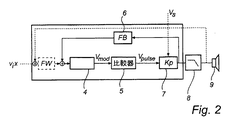
図1のPMAの1つの実施例が図2に示され、これは、制御ブロック4、比較器5、フィードバックブロック6、及びスイッチング電力段7を含む。制御ブロック4は、自励発振を保証するためにフィードバックブロック6と協働する伝達関数を有する。図2のPMAは、限定ではないが、引用により本明細書に組み込まれる本出願人の国際特許出願WO98/19391で説明される制御振動変調器(COM)などの自励式発振変調器に基づいている。他の自励式発振原理は、積分器、ヒステリシス又は非ヒステリシス制御、或いは当業者には明らかな他の何らかの自励式発振変調器原理に基づいて使用することができる。
One embodiment of the PMA of FIG. 1 is shown in FIG. 2 and includes a control block 4, a
実際には、パルス変調は、パルス幅変調に限定されないが、パルス密度変調(PDM)、パルス位置変調(PPM)、又は当業者には公知の他の何らかのパルス変調方式といったあるタイプのパルス変調である。 In practice, pulse modulation is not limited to pulse width modulation, but is a type of pulse modulation such as pulse density modulation (PDM), pulse position modulation (PPM), or some other pulse modulation scheme known to those skilled in the art. is there.
COM変調器がPMAに含まれる場合、以下の式が適用される。
Vo=(Vs/Vmod)・Vi=A・Vi
ここで、Voはスイッチング段7の出力電圧、ViはPMAへの入力基準信号、Vsは、電源からの駆動電圧、Vmodは、比較器5への入力信号であり、Aは、電力段利得である。
If a COM modulator is included in the PMA, the following equation applies:
V o = (V s / V mod ) · V i = A · V i
Where V o is the output voltage of the switching
電圧Vmodは、COM変調器の制御された不安定性に起因して、電力段電圧に振幅で比例して変化することになり、従って電力段利得が保持される(Aは定数になる)。一定の電力段利得は無限PSRRを意味することになり、従って、COM変調器を含むPMAは、理論的には無限PSRRを得ることができる。よって、歪みはPMAの出力で生成されないことになる。 The voltage V mod will vary proportionally with the amplitude of the power stage voltage due to the controlled instability of the COM modulator, thus maintaining the power stage gain (A becomes a constant). A constant power stage gain will mean infinite PSRR, so a PMA including a COM modulator can theoretically obtain infinite PSRR. Therefore, no distortion is generated at the output of the PMA.
図1に示されるように、電源は複数のPMA1、1´を駆動することができる。
As shown in FIG. 1, the power supply can drive a plurality of
図2では、PMAスイッチング電力段からの出力が、トランスデューサ(拡声器)のような負荷9に接続された復調フィルタ8に接続される。或いは(図示せず)、スイッチング段出力は、引用により本明細書に組み込まれるWO02/093973で説明される「パルス変調トランスデューサ」の原理によるトランスデューサに直接接続され、又はこれと完全に一体化される。
In FIG. 2, the output from the PMA switching power stage is connected to a
電源は、入力電圧viに基づいて、図1に示されたPMAの各々のスイッチング段7に必要な駆動電圧Vsを供給することになる。電圧源は、次式の範囲内で変化する電圧Vsを供給可能でなければならない。
Vs=[Δ;Vo,max+Δ]=[Δ;A・Vi+Δ]
ここでVo,maxは、A・Viと等しいPMAスイッチング電力段の要求される最大出力電圧であり、Δは、任意選択のヘッドルームである。値Δは、時間変数とすることができ、PMAがブーストトポロジー(以下を参照)に基づく場合に負とすることができる。
The power supply will supply the necessary drive voltage V s to each switching
V s = [Δ; V o, max + Δ] = [Δ; A · V i + Δ]
Where V o, max is the required maximum output voltage of the PMA switching power stage equal to A · V i, and Δ is the optional headroom. The value Δ can be a time variable and can be negative if the PMA is based on a boost topology (see below).
電源は、図1に示されたPMAのいずれかの最大ピーク出力電圧Vo,maxに電圧ヘッドルームを供給する必要がある。 The power supply needs to supply voltage headroom to the maximum peak output voltage V o, max of any of the PMAs shown in FIG.
PMAが平衡され、単一の可変駆動電圧によって駆動される場合、この電圧は、次式によって求めることができる。
Vs=A・max(|Vix|)+Δ (1)
ここで、vixは図1に示されるような種々のPMA入力基準であり、Aは電力段利得である。
If the PMA is balanced and driven by a single variable drive voltage, this voltage can be determined by the following equation:
V s = A · max (| V ix |) + Δ (1)
Where v ix is the various PMA input criteria as shown in FIG. 1, and A is the power stage gain.
電圧源の実施形態の第1の実施例が、絶縁されたシステム、例えば絶縁スピーカー、又はバッテリー駆動システムでの実施形態の非ガルバニ絶縁バックコンバータとして図2に示されている。 A first example of an embodiment of a voltage source is shown in FIG. 2 as an embodiment of a non-galvanic isolation buck converter in an isolated system, such as an isolated speaker, or battery powered system.
回路は、パルス変調入力電圧に接続されたゲート11、コイル14を介して出力端子の第1側13に接続されたソース12、及び整流された主電源5の一方側16に接続されたドレイン15を有するMOSFET10を含む。整流された主電源の他方の側17は、出力端子の第2側18に接続される。この第2出力側18にはMOSFETドレイン15へのコンデンサ19及びMOSFETソース12へのダイオード20が接続される。最後に、出力コンデンサ21は出力端子の第1及び第2側13、18を橋絡する。
The circuit comprises a
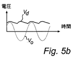
増幅器スイッチング段の等価負荷抵抗Raが、迅速に電源出力キャパシタンスCoを放電でき、RaCo時定数によって十分に低い負のdV/dtが式1に記述されたような電圧を供給できるように電源の出力キャパシタンスは、十分小さいのが好ましい。場合によっては、ヘッドルームΔは、パルス発生器が負のdV/dtを有する電圧を供給するときに一定となる。これにより、図5aに示されるような式1に従う駆動電圧が生じることになる。
The output of the power supply so that the equivalent load resistance Ra of the amplifier switching stage can quickly discharge the power supply output capacitance Co, and the sufficiently low negative dV / dt can be supplied by the RaCo time constant as described in
しかしながら、大きなキャパシタンス21が図3の電源の出力に配置される場合、電源は、キャパシタンスから電流をシンクできなくなる。従って、出力電圧Vdに必要な負のdV/dtを供給できない。言い換えると、電源電圧Vsが負のdV/dtを有する場合、コンバータは正弦波信号の周期の2/4でPMA出力信号を追従できない場合がある。これにより、図5bによる駆動電圧を生じることになる。
However, if a
大きな出力キャパシタンスに更に適した電圧源の第2の実施例を、図4に示している。トポロジーは、フライバックで生成され、ガルバニ絶縁を含むことができる。 A second embodiment of a voltage source more suitable for large output capacitance is shown in FIG. The topology is generated with a flyback and can include galvanic insulation.
この回路は、整流された主電源5の2つの側間に変圧器27の一次巻線26に直列に接続されたMOSFET25を含む。変調入力電圧は、一次側MOSFET25のゲート28に接続される。変圧器26の第1の二次巻線29は、二次側MOSFET31のゲート30に1つの端29aにおいて接続される。別の二次巻線38は、出力端子の第1側32に1つの端38bにおいて接続される。出力端子の第2側33は、MOSFETのドレイン34に接続され、MOSFETのソース35は、2つの二次側巻線29、38の他方の端29b、38aに接続される。この場合も出力コンデンサ36は、出力端子の第1及び第2側32、33を橋絡する。
This circuit includes a
更に、制御入力37は、MOSFETゲート30に接続される。MOSFET31は、MOSFET25がターンオンされた場合に誘起されるパルスによって該MOSFET25がターンオンされる時のアクティブダイオードとして動作する。更にMOSFET31は、MOSFET25がターンオフされた時の変圧器電圧逆転期間中に出力端子33からの電流のシンクを可能にする。
Further, the control input 37 is connected to the
図4の電圧源は、電流シンクが可能となり、従って、より低い負のdV/dtを生成することができる。図4の回路はまた、付加的なアクティブMOSFET31により、通常の二次順方向ダイオード(図2の20)のダイオード電圧降下が無いという利点を有する。これは、電源の高電流出力振幅において効率が高くなる。
The voltage source of FIG. 4 allows current sinking and can therefore produce a lower negative dV / dt. The circuit of FIG. 4 also has the advantage that the additional
当業者であれば、「バッキング(Bucking)」(コンバータ入力電圧に対してコンバータ出力電圧を低下させる)が可能などのようなトポロジーも使用できることを理解している。順方向、プッシュプル、CUK、Sephic、又はバック系の他のいずれかのコンバータタイプのような他のトポロジーも「バッキング」に使用できる。 One skilled in the art understands that any topology capable of “buking” (lowering the converter output voltage relative to the converter input voltage) can be used. Other topologies such as forward, push-pull, CUK, Sepic, or any other converter type in the buck system can also be used for “backing”.
幾つかのバッテリー駆動システムなどの低供給電圧PAMシステムの場合には、電源は、ブーストトポロジーとして実装できる(図示せず)。これによって、PAMシステムの出力電圧は、電圧源の供給電圧の出力電圧を越えることができる。ブースト、プッシュプル、又は「ブースティング」可能な当業者には既知の他の何らかのコンバータタイプのようなトポロジーも電圧源として使用できる。 For low supply voltage PAM systems, such as some battery powered systems, the power supply can be implemented as a boost topology (not shown). Thereby, the output voltage of the PAM system can exceed the output voltage of the supply voltage of the voltage source. Topologies such as boost, push-pull, or some other converter type known to those skilled in the art that can be “boosted” can also be used as a voltage source.
PMAがシングルエンドされ、デュアル駆動電圧によって駆動される場合、この電圧は次式で求められる。
正の供給電圧Vd:
Vs=A・max(|Vix|)+Δ
負の供給電圧Vs:
Vd=−A・max(|Vix|)−Δ
If the PMA is single-ended and driven by a dual drive voltage, this voltage is determined by:
Positive supply voltage V d :
V s = A · max (| V ix |) + Δ
Negative supply voltage V s :
V d = −A · max (| V ix |) −Δ
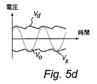
図5a及び5bのシングル駆動電圧に対応するデュアル駆動電圧の実施例を図5c及び5dに示している。スイッチング出力電圧Voは、図では単に概略的に示されている。 Examples of dual drive voltages corresponding to the single drive voltages of FIGS. 5a and 5b are shown in FIGS. 5c and 5d. The switching output voltage V o is shown only schematically in the figure.
図6は、図1の電力コンバータの変形を示しており、電源4からの駆動電圧信号Vs経路が、弱電圧振幅の信号であるPMA入力電圧Vi1及びVi2を伝えるのに使用される。図示された実施例では、入力信号Vi1及びVi2は、加算ブロック39で電源駆動信号に単純に重畳され、後でPMAにおいて抽出される。
FIG. 6 shows a variation of the power converter of FIG. 1, where the drive voltage signal V s path from the power supply 4 is used to carry the PMA input voltages V i1 and V i2 , which are weak voltage amplitude signals. . In the illustrated embodiment, the input signals V i1 and V i2 are simply superimposed on the power supply drive signal at the summing
入力信号Vi1、Vi2はまた、本質的に、当業者に知られたどのような公知の変調方式によっても空間を介して送信することができる。入力信号は、実施形態に応じてPMA又はPMTでデジタル送信器及び受信器が必要となるデジタル信号であるのが好ましい。全チャンネル間でこの単一結線を実現するため、コンピュータネットワーク又はADSL/xDSL通信システムによる方法を利用することができるのが好ましい。 The input signals V i1 and V i2 can also be transmitted over space by essentially any known modulation scheme known to those skilled in the art. The input signal is preferably a digital signal that requires a digital transmitter and receiver at the PMA or PMT, depending on the embodiment. In order to realize this single connection between all channels, it is preferable that a method by a computer network or an ADSL / xDSL communication system can be used.
本発明のこの実施形態は、自動車用途又はマルチチャンネルシステムで使用できるのが好ましい。 This embodiment of the invention is preferably usable in automotive applications or multi-channel systems.
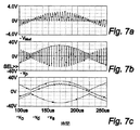
図7a−cは、COM技術を使用し、デュアル電源により動作する1つのスイッチングレッグを含むシングルエンドPMAを有する1つのPMA1を備えた図1のシステムのシミュレーションを示している。
FIGS. 7 a-c show a simulation of the system of FIG. 1 with a
図7aは、比較器入力信号Vmodを示し、図7bはスイッチング段からの差動電力出力Vpを示す。図7cは、図5dによる信号波形を有する駆動電圧の2つの部分、Vs及びVdを示す。図7cは更に、PMA出力フィルタの出力電圧Voを示す。 FIG. 7a shows the comparator input signal V mod and FIG. 7b shows the differential power output V p from the switching stage. FIG. 7c shows two parts of the drive voltage, V s and V d , having the signal waveform according to FIG. 5d. FIG. 7c further shows the output voltage V o of the PMA output filter.
比較器入力信号Vmodは、通常はCOM変調用である駆動電圧振幅に応じて変化することが図7aから分かる。これは、PMAでの一定の電力段利得を示し、比Vo/Vmodが一定である場合に非常に高い電源除去比を生成することになる。 It can be seen from FIG. 7a that the comparator input signal V mod varies with the drive voltage amplitude, which is usually for COM modulation. This represents a constant power stage gain at the PMA, and will produce a very high power supply rejection ratio when the ratio V o / V mod is constant.
更に図7bは、本発明によるパルス振幅幅変調PAWMの特性を示す。PAWMではデューティサイクルがほぼ一定である点に留意されたい。これは、ほとんど理想的な振幅変調が支配的であることに起因する。同じ電源から複数のPMAを動作する場合、当業者は、デューティサイクルの変化が出力信号の1つの期間にわたってPMAの一部又は全てにおいて生じる可能性があることが分かるであろう。 Furthermore, FIG. 7b shows the characteristics of a pulse amplitude width modulated PAWM according to the invention. Note that in PAWM, the duty cycle is nearly constant. This is due to the fact that almost ideal amplitude modulation is dominant. When operating multiple PMAs from the same power source, those skilled in the art will appreciate that changes in duty cycle may occur in some or all of the PMAs over one period of the output signal.
図7cのPMA出力信号Voは、振幅変調信号及びパルス幅変調信号により与えられた低周波信号を含む。更に、この電圧信号は、PMAパルス幅変調によりもたらされた高周波信号残余物を含む。高周波信号成分振幅は、従来の2つのレベルPWMに比べて低く(及び変調指数に比例する)、これは一定のデュアル駆動電圧を有する従来技術の電力コンバータからの信号を表す図9から分かる。 PMA output signal V o of Figure 7c includes a low-frequency signal supplied by the amplitude modulation signal and a pulse width modulation signal. In addition, this voltage signal contains high frequency signal remnants brought about by PMA pulse width modulation. The high frequency signal component amplitude is low (and proportional to the modulation index) compared to the conventional two level PWM, which can be seen from FIG. 9, which represents the signal from a prior art power converter with a constant dual drive voltage.
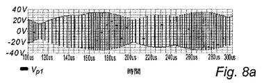
図8では、2つのPMAを備えたマルチチャンネルシステムのような図2のシステムのシミュレーションを示している。PMA1及び1´のスイッチング電力段7からの出力信号Vp1及びVp2が、図8a及び図8bに示されている。ローパスフィルター処理された出力Vo1及びVo2、及び駆動電圧の2つの部分Vs及びVdは図8cに示されている。
FIG. 8 shows a simulation of the system of FIG. 2, such as a multi-channel system with two PMAs. The output signals V p1 and V p2 from the switching
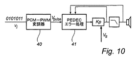
本発明の別の好ましい実施形態が図10に示され、これはPMAがデジタルPCM−PWM変調器40に基づき、制御システム41がPMAに加えられているPAMシステムを示している。制御システム41は、好ましくは、引用により本明細書に組み込まれる国際公開番号WO98/44626の本出願人の特許において説明されているようなPEDEC制御システムとすることができる。このようなシステムは、高PSRRを得ることができる。他の高PSRRフィードバックシステムは、デジタル変調ベースのPMAに適用することができる。
Another preferred embodiment of the present invention is shown in FIG. 10, which shows a PAM system in which the PMA is based on a digital PCM-
別の好ましい実施形態は、PAM変調技術であり、この場合、電源出力電圧は、PMAピーク出力電圧によって所定時間ウィンドウ内の固定電圧レベルに制御される。従って、電源出力電圧Vdのピーク検出変調を得る。このような電圧源制御の結果を、図11に示している。Vdはやはり電源2からの駆動電圧であり、Voは復調フィルタ9からの出力電圧である。有利には、このピーク信号検出は、いずれの時間であっても最大出力電圧及び従って最大要求電源レベルを決定付けるボリューム制御情報から導くことができる。従ってシステムは、電圧源2に対しこの情報を提供する手段を含む。
Another preferred embodiment is a PAM modulation technique, where the power supply output voltage is controlled to a fixed voltage level within a predetermined time window by the PMA peak output voltage. Therefore, to obtain a peak detection modulation of the power supply output voltage V d. The result of such voltage source control is shown in FIG. V d is also a drive voltage from the
更に別の好ましい実施形態は、PAM変調技術であり、この場合、電源出力電圧がPMAピーク出力電圧によって制御される(図示せず)。電源電圧は、ピーク検出が電源電圧を上昇させるまで降下することになる。 Yet another preferred embodiment is a PAM modulation technique, where the power supply output voltage is controlled by the PMA peak output voltage (not shown). The power supply voltage will drop until peak detection increases the power supply voltage.
本発明は、有利には、AC−AC、DC−DC、DC−AC、AC−DC、又は上述されたいずれかの組合せ、好ましくはDC−AC高精度音声電力変換システムなどの何らかの所与の電力変換システムにおいて実施することができ、この場合、電力段素子は、「オン」又は「オフ」状態のいずれかで動作する。 The present invention advantageously provides any given, such as AC-AC, DC-DC, DC-AC, AC-DC, or any combination described above, preferably a DC-AC high precision audio power conversion system. It can be implemented in a power conversion system, where the power stage element operates in either an “on” or “off” state.
1 PMA
2 電圧源
3 主電源
8 復調フィルタ
9 負荷
1 PMA
2 Voltage source 3
Claims (15)
各増幅器に駆動電圧(Vs、Vd)を供給する電圧源(2)と、
を備えた電力変換システムにおいて、
前記電圧源(2)は、前記入力基準(vi)が供給され、該入力基準(vi)の増幅された絶対値に追従する第1駆動電圧成分(Vd)を供給するよう構成されていることを特徴とする電力変換システム。 A pulse modulator (4, 5, 6; 40) for generating a pulse modulated signal (v pulse ) based on a reference input (v i ) and a switching power stage (a) configured to amplify the pulse modulated signal ( 7) and at least one pulse modulation amplifier (PMA) (1) comprising a control system (6; 40) configured to compensate for power supply voltage changes;
A voltage source (2) for supplying a drive voltage (V s , V d ) to each amplifier;
In the power conversion system with
The voltage source (2), the input reference (v i) is supplied, is configured to supply a first driving voltage component follows the amplified absolute value of the input reference (v i) (V d) A power conversion system characterized by that.
Applications Claiming Priority (2)
| Application Number | Priority Date | Filing Date | Title |
|---|---|---|---|
| SE0302681A SE0302681D0 (en) | 2003-10-09 | 2003-10-09 | Method of pulse area modulation |
| PCT/IB2004/003267 WO2005036731A2 (en) | 2003-10-09 | 2004-10-07 | Power conversion system |
Publications (1)
| Publication Number | Publication Date |
|---|---|
| JP2007508731A true JP2007508731A (en) | 2007-04-05 |
Family
ID=29398701
Family Applications (1)
| Application Number | Title | Priority Date | Filing Date |
|---|---|---|---|
| JP2006530749A Abandoned JP2007508731A (en) | 2003-10-09 | 2004-10-07 | Power conversion system |
Country Status (7)
| Country | Link |
|---|---|
| US (1) | US7321262B2 (en) |
| EP (1) | EP1671420A2 (en) |
| JP (1) | JP2007508731A (en) |
| KR (1) | KR20060120002A (en) |
| CN (1) | CN1864324A (en) |
| SE (1) | SE0302681D0 (en) |
| WO (1) | WO2005036731A2 (en) |
Cited By (2)
| Publication number | Priority date | Publication date | Assignee | Title |
|---|---|---|---|---|
| US8686792B2 (en) | 2010-01-07 | 2014-04-01 | Panasonic Corporation | Amplifying device |
| JP2015142378A (en) * | 2014-01-30 | 2015-08-03 | シモンズ プレシジョン プロダクツ, インク.Simmonds Precision Products,Inc. | Signal communication method and communication system |
Families Citing this family (19)
| Publication number | Priority date | Publication date | Assignee | Title |
|---|---|---|---|---|
| FR2890258B1 (en) * | 2005-08-30 | 2007-10-12 | Thales Sa | DEVICE AND METHOD FOR AMPLIFYING IMPULSE RF SIGNALS |
| KR100710509B1 (en) * | 2006-04-11 | 2007-04-25 | 남상욱 | High-efficiency linear power amplifier system using pulse area modulation |
| US7852150B1 (en) * | 2007-12-20 | 2010-12-14 | The Tc Group A/S | Switching amplifier driven by a controlled power supply |
| US8995691B2 (en) | 2008-07-14 | 2015-03-31 | Audera Acoustics Inc. | Audio amplifier |
| US8280070B2 (en) * | 2008-08-20 | 2012-10-02 | Siemens Industry, Inc. | Arrangement and method for communicating audio and DC signals |
| US8350537B2 (en) * | 2010-03-04 | 2013-01-08 | Bose Corporation | Power supply transient response improving |
| US7986187B1 (en) | 2010-03-04 | 2011-07-26 | Bose Corporation | Versatile audio power amplifier |
| US8384478B2 (en) * | 2010-03-04 | 2013-02-26 | Bose Corporation | Versatile audio power amplifier |
| JP5903638B2 (en) * | 2010-06-25 | 2016-04-13 | パナソニックIpマネジメント株式会社 | Amplification equipment |
| CN103078510B (en) | 2011-10-25 | 2015-11-25 | 通用电气公司 | Resonant power, magnetic resonance imaging system and control method |
| CN103078515A (en) | 2011-10-25 | 2013-05-01 | 通用电气公司 | Resonant power supply, converter controller, magnetic resonance imaging system and control method |
| CN103076580B (en) | 2011-10-25 | 2016-02-03 | 通用电气公司 | Gradient amplifier, circuit control device, magnetic resonance imaging system and control method |
| US9839967B2 (en) | 2011-11-08 | 2017-12-12 | Lincoln Global, Inc. | System and method for real-time computation and reporting of welding machine performance and metrics |
| DE102012104488A1 (en) * | 2012-05-24 | 2013-11-28 | Hochschule für angewandte Wissenschaften München | Switched amplifier for variable supply voltage |
| US9319495B2 (en) | 2013-08-06 | 2016-04-19 | Aura Semiconductor Pvt. Ltd | Power amplifier providing high efficiency |
| CN103607176B (en) * | 2013-10-21 | 2017-05-24 | 梁秀红 | Audio power amplifier power supply circuit control method, audio power amplifier power supply circuit and audio power amplifier circuit |
| US20160142832A1 (en) | 2014-11-19 | 2016-05-19 | Martin Evert Gustaf Hillbratt | Signal Amplifier |
| US9559642B2 (en) | 2015-01-02 | 2017-01-31 | Logitech Europe, S.A. | Audio delivery system having an improved efficiency and extended operation time between recharges or battery replacements |
| JPWO2017154051A1 (en) * | 2016-03-08 | 2019-01-17 | パナソニックIpマネジメント株式会社 | Class D amplifier and sound reproducing apparatus |
Family Cites Families (15)
| Publication number | Priority date | Publication date | Assignee | Title |
|---|---|---|---|---|
| US3900823A (en) * | 1973-03-28 | 1975-08-19 | Nathan O Sokal | Amplifying and processing apparatus for modulated carrier signals |
| US5075634A (en) * | 1990-11-23 | 1991-12-24 | Blade Technologies Inc. | Composite bridge amplifier |
| WO1994011799A1 (en) * | 1992-11-10 | 1994-05-26 | Motorola, Inc. | Switching regulator and amplifier system |
| DE69409968T2 (en) | 1993-11-30 | 1998-10-29 | Crown Int | SWITCHING POWER SUPPLY FOR A POWER AMPLIFIER |
| US5898340A (en) * | 1996-11-20 | 1999-04-27 | Chatterjee; Manjirnath A. | High power efficiency audio amplifier with digital audio and volume inputs |
| US5998340A (en) * | 1997-03-07 | 1999-12-07 | Hitachi Maxell, Ltd. | Lubricant and magnetic recording medium using the same |
| US6388514B1 (en) * | 1998-12-23 | 2002-05-14 | International Rectifier Corporation | Class D high voltage amplifier system with adaptive power supply |
| WO2000070754A1 (en) | 1999-05-19 | 2000-11-23 | Jam Technologies, Llc | Distortion reduction technique for inductive boost amplifier |
| US6198347B1 (en) * | 1999-07-29 | 2001-03-06 | Tropian, Inc. | Driving circuits for switch mode RF power amplifiers |
| US6816016B2 (en) * | 2000-08-10 | 2004-11-09 | Tropian, Inc. | High-efficiency modulating RF amplifier |
| US6373340B1 (en) * | 2000-08-14 | 2002-04-16 | K. S. Waves, Ltd. | High-efficiency audio power amplifier |
| US6496059B1 (en) * | 2000-11-17 | 2002-12-17 | Tranh T. Nguyen | Clas-N amplifer |
| SE0104403D0 (en) | 2001-12-21 | 2001-12-21 | Bang & Olufsen Powerhouse As | Attenuation control for digital power converters |
| US6765436B1 (en) * | 2002-09-04 | 2004-07-20 | Cirrus Logic, Inc. | Power supply based audio compression for digital audio amplifier |
| JP4445304B2 (en) * | 2004-03-26 | 2010-04-07 | オンキヨー株式会社 | Switching amplifier |
-
2003
- 2003-10-09 SE SE0302681A patent/SE0302681D0/en unknown
-
2004
- 2004-10-07 KR KR1020067006545A patent/KR20060120002A/en not_active Application Discontinuation
- 2004-10-07 CN CNA2004800290348A patent/CN1864324A/en active Pending
- 2004-10-07 JP JP2006530749A patent/JP2007508731A/en not_active Abandoned
- 2004-10-07 EP EP04769576A patent/EP1671420A2/en not_active Ceased
- 2004-10-07 WO PCT/IB2004/003267 patent/WO2005036731A2/en active Application Filing
- 2004-10-07 US US10/570,324 patent/US7321262B2/en not_active Expired - Fee Related
Cited By (3)
| Publication number | Priority date | Publication date | Assignee | Title |
|---|---|---|---|---|
| US8686792B2 (en) | 2010-01-07 | 2014-04-01 | Panasonic Corporation | Amplifying device |
| JP5635507B2 (en) * | 2010-01-07 | 2014-12-03 | パナソニック株式会社 | Amplifier |
| JP2015142378A (en) * | 2014-01-30 | 2015-08-03 | シモンズ プレシジョン プロダクツ, インク.Simmonds Precision Products,Inc. | Signal communication method and communication system |
Also Published As
| Publication number | Publication date |
|---|---|
| CN1864324A (en) | 2006-11-15 |
| WO2005036731A3 (en) | 2005-06-16 |
| US20070109044A1 (en) | 2007-05-17 |
| KR20060120002A (en) | 2006-11-24 |
| WO2005036731A2 (en) | 2005-04-21 |
| EP1671420A2 (en) | 2006-06-21 |
| US7321262B2 (en) | 2008-01-22 |
| SE0302681D0 (en) | 2003-10-09 |
Similar Documents
| Publication | Publication Date | Title |
|---|---|---|
| JP2007508731A (en) | Power conversion system | |
| US7952426B2 (en) | Digital audio amplifier and digital audio amplifying method therefor | |
| US7567443B2 (en) | Power converter | |
| CN112954544B (en) | Driving circuit | |
| US7696816B2 (en) | System and method for minimizing DC offset in outputs of audio power amplifiers | |
| US9444419B2 (en) | Boosted differential class H amplifier | |
| US6476674B2 (en) | Method and apparatus for error correction of amplifier | |
| CN112514247A (en) | Self-boosting amplifier | |
| JP2012156616A (en) | Semiconductor integrated circuit and method of operating the same | |
| US10749486B2 (en) | Class D amplifier current feedback | |
| US6963189B2 (en) | Attenuation control for digital power converters | |
| US7408403B2 (en) | Circuits and methods for amplifying signals | |
| JP2004515091A (en) | Power amplifier for parametric speakers | |
| US7295062B2 (en) | Pulse modulated power converter | |
| JP2004128662A (en) | Digital amplifier | |
| KR100453708B1 (en) | High-Efficiency Switching Amplifier | |
| US11159132B2 (en) | Class D amplifier stereo to mono converter | |
| US11121682B1 (en) | Single-stage boost class-D amplifier | |
| JP2005341327A (en) | Power amplification apparatus | |
| US7889001B2 (en) | Systems and methods of reduced distortion in a class D amplifier | |
| JP2001237649A (en) | Amplifier |
Legal Events
| Date | Code | Title | Description |
|---|---|---|---|
| A621 | Written request for application examination |
Free format text: JAPANESE INTERMEDIATE CODE: A621 Effective date: 20071009 |
|
| A762 | Written abandonment of application |
Free format text: JAPANESE INTERMEDIATE CODE: A762 Effective date: 20090730 |
|
| A521 | Written amendment |
Free format text: JAPANESE INTERMEDIATE CODE: A821 Effective date: 20090730 |