JP2007508547A - Solid state reference electrode - Google Patents
Solid state reference electrode Download PDFInfo
- Publication number
- JP2007508547A JP2007508547A JP2006534316A JP2006534316A JP2007508547A JP 2007508547 A JP2007508547 A JP 2007508547A JP 2006534316 A JP2006534316 A JP 2006534316A JP 2006534316 A JP2006534316 A JP 2006534316A JP 2007508547 A JP2007508547 A JP 2007508547A
- Authority
- JP
- Japan
- Prior art keywords
- reference electrode
- conductive support
- electrode according
- hydrophobic layer
- insulating hydrophobic
- Prior art date
- Legal status (The legal status is an assumption and is not a legal conclusion. Google has not performed a legal analysis and makes no representation as to the accuracy of the status listed.)
- Ceased
Links
Images


Classifications
-
- G—PHYSICS
- G01—MEASURING; TESTING
- G01N—INVESTIGATING OR ANALYSING MATERIALS BY DETERMINING THEIR CHEMICAL OR PHYSICAL PROPERTIES
- G01N27/00—Investigating or analysing materials by the use of electric, electrochemical, or magnetic means
- G01N27/26—Investigating or analysing materials by the use of electric, electrochemical, or magnetic means by investigating electrochemical variables; by using electrolysis or electrophoresis
- G01N27/28—Electrolytic cell components
- G01N27/30—Electrodes, e.g. test electrodes; Half-cells
- G01N27/301—Reference electrodes
Abstract
第1の表面を有する導電性支持体と、複数の非選択性イオン交換部位を有する、前記第1の表面に隣接したイオン絶縁性の疎水性層とを含む参照電極。 A reference electrode comprising a conductive support having a first surface and an ion insulating hydrophobic layer adjacent to the first surface and having a plurality of non-selective ion exchange sites.
Description
本発明は、一般にはソリッドステート参照電極の分野に関し、さらに詳細には電気化学的なソリッドステート参照電極(solid state electrochemical reference electrodes)に関する。 The present invention relates generally to the field of solid state reference electrodes, and more particularly to electrochemical solid state electrochemical reference electrodes.
電気化学的な測定においては、化学的な“基準電位”を電気化学センサー(たとえばpHセンサー)と組み合わせて使用することが多い。基準電位は、電気回路における接地電位に類似している。ほとんどの場合、基準電位は、別個の対照セル(このとき対照セルは、試験溶液とイオン連通状態にある)中に浸漬される参照電極から得られる。参照電極は一般に、銀もしくは水銀金属と接触している不溶性の銀塩または水銀塩を介して基準電位を生じる。対照セルにおいては一般に、試験溶液とイオン的な接触状態にある導電性のイオン溶液中に塩が含有されている。対照セルのイオン溶液と試験溶液との間のイオン的接触は一般に、イオンが対照セルから試験溶液に流れるのを、およびこの逆に流れるのを可能にするような多孔質層によってもたらされる。これらのシステムの多くがもつ1つの問題は、多孔質層を通過するイオン流量が少なすぎる場合は、測定値にドリフトが入り込むことがあるということ、そしてイオン流量が多すぎる場合は、イオン溶液が試験溶液に対する汚染源になることがあるということである(この逆の場合もある)。 In electrochemical measurements, a chemical “reference potential” is often used in combination with an electrochemical sensor (eg, a pH sensor). The reference potential is similar to the ground potential in the electric circuit. In most cases, the reference potential is obtained from a reference electrode that is immersed in a separate control cell, where the control cell is in ionic communication with the test solution. The reference electrode generally generates a reference potential via an insoluble silver or mercury salt that is in contact with silver or mercury metal. In control cells, the salt is generally contained in a conductive ionic solution that is in ionic contact with the test solution. The ionic contact between the ionic solution of the control cell and the test solution is generally provided by a porous layer that allows ions to flow from the control cell to the test solution and vice versa. One problem with many of these systems is that if the ion flow rate through the porous layer is too low, the measurement may drift, and if the ion flow rate is too high, the ionic solution It can be a source of contamination for the test solution (and vice versa).
本発明は、一般には電気化学的なソリッドステート参照電極に関する。本発明による電気化学的なソリッドステート参照電極は、測定ドリフトを減少させるだけでなく、試験溶液に対する汚染も少なくすることがある。本発明の電気化学的なソリッドステート参照電極はさらに、よりコスト効率が良くて且つ時宜にかなった方法で製造することができ、従来の多くの参照電極構造物より信頼性が高い場合がある。 The present invention relates generally to electrochemical solid state reference electrodes. An electrochemical solid state reference electrode according to the present invention not only reduces measurement drift, but may also reduce contamination to the test solution. The electrochemical solid state reference electrode of the present invention can also be manufactured in a more cost effective and timely manner and may be more reliable than many conventional reference electrode structures.
本発明の1つの実施態様においては、第1の表面を有する導電性支持体と、前記第1の表面に隣接したイオン絶縁性の疎水性層とを含む参照電極が提供される。イオン絶縁性の疎水性層は、その露出表面上に複数の非選択性イオン交換部位を有する。イオン絶縁性の疎水性層が試験溶液にさらされると、イオン交換部位のために、イオン絶縁性の疎水性層の表面上にイオン電荷が生じる。イオン絶縁性の疎水性層が導電性支持体に隣接して設けられているので、対応するミラー電荷が導電性支持体に生じ、したがって導電性支持体において対応する基準電位が得られる。幾つかの実施態様においては、露出したイオン交換部位の数を増やすために、したがって参照電極の感度を上げるために、イオン絶縁性の疎水性層の上もしくは中に非選択性イオン交換層がさらに設けられる。幾つかの実施態様においては、非選択性イオン交換層は非選択性イオン交換ゼオライト層である。しかしながら、用途に応じて、いかなる適切な非選択性イオン交換層も使用することができる。 In one embodiment of the present invention, a reference electrode is provided that includes a conductive support having a first surface and an ionically insulating hydrophobic layer adjacent to the first surface. The ion insulating hydrophobic layer has a plurality of non-selective ion exchange sites on its exposed surface. When the ion insulating hydrophobic layer is exposed to the test solution, an ionic charge is generated on the surface of the ion insulating hydrophobic layer due to ion exchange sites. Since the ion-insulating hydrophobic layer is provided adjacent to the conductive support, a corresponding mirror charge is generated on the conductive support, and thus a corresponding reference potential is obtained at the conductive support. In some embodiments, a non-selective ion exchange layer is further provided on or in the ion insulating hydrophobic layer to increase the number of exposed ion exchange sites and thus increase the sensitivity of the reference electrode. Provided. In some embodiments, the non-selective ion exchange layer is a non-selective ion exchange zeolite layer. However, any suitable non-selective ion exchange layer can be used depending on the application.
幾つかの実施態様においては、導電性支持体上に生成する基準電位を、電気回路(増幅器など)の高インピーダンスインプットに供給する。たとえば、基準電位を、電界効果トランジスタ(FET)のゲートに、または他のあらゆる適切な高インピーダンス回路に供給することができる。他の実施態様においては、基準電位をFETの支持体に供給することができる。このように供給するときに、FETのゲートを試験溶液中の電気化学センサーのアウトプットに接続することができる。支持体における基準電位は、電気化学センサーによってもたらされる所定のゲート電圧でのFETから供給される電流を相殺、補償するのに役立つことがある。このようなFET構造物は、電気変換器に良好な化学をもたらすのに役立つことがある。 In some embodiments, a reference potential generated on the conductive support is supplied to a high impedance input of an electrical circuit (such as an amplifier). For example, a reference potential can be supplied to the gate of a field effect transistor (FET) or to any other suitable high impedance circuit. In other embodiments, a reference potential can be supplied to the FET support. When fed in this way, the gate of the FET can be connected to the output of the electrochemical sensor in the test solution. The reference potential at the support may help to offset and compensate for the current supplied from the FET at a given gate voltage provided by the electrochemical sensor. Such FET structures can help bring good chemistry to the electrical converter.
本発明は種々の変更態様や代替態様が可能であるけれども、特定の態様について、図面に示して詳細に説明する。しかしながら、理解しておかなければならないことは、こうした説明は、本発明を特定の実施態様に限定することを意図しているわけではない、という点である。これに反し、本発明は、本発明の精神と範囲内に含まれる全ての変更態様、同等態様、および代替態様を包含するものとする。 While the invention is susceptible to various modifications and alternative forms, specific embodiments have been shown in the drawings and will be described in detail. However, it should be understood that these descriptions are not intended to limit the invention to a particular embodiment. On the contrary, the invention is intended to cover all modifications, equivalents, and alternatives falling within the spirit and scope of the invention.
以下に図面を参照しつつ説明する。別々の図面における同様の要素は、同様の仕方で番号付けされている。図面(必ずしもスケールどおりではない)は、選択された実施態様を示しており、本発明の範囲を限定することを意図したものではない。種々の要素に関して、種々の構造、寸法、および材料の例を示すことができるけれども、当業者であれば、提供される例の多くが、使用可能である適切な代替態様を有する、ということがわかるであろう。 This will be described below with reference to the drawings. Similar elements in different drawings are numbered in a similar manner. The drawings (not necessarily to scale) show selected embodiments and are not intended to limit the scope of the invention. Although examples of various structures, dimensions, and materials can be given for various elements, those skilled in the art will appreciate that many of the examples provided have suitable alternatives that can be used. You will understand.
本発明は、一般には参照電極(たとえば電気化学的なソリッドステート参照電極)に関する。本発明は、必要に応じて、あらゆる電位差測定法、電流測定法、およびボルタンメトリー法での使用に対して適用可能である。本発明の種々の態様に対する理解が、下記の種々の実施態様と例についての説明によって得られる(但し、本発明がこれによって限定されることはない)。 The present invention relates generally to reference electrodes (eg, electrochemical solid state reference electrodes). The present invention is applicable for use in any potentiometric, amperometric and voltammetric methods as desired. An understanding of the various aspects of the invention will be gained from the description of the various embodiments and examples set forth below (although the invention is not so limited).
図1は、本発明の1つの実施態様による参照電極100の断面図である。参照電極100は、第1の表面115を有する導電性支持体110を含む。イオン絶縁性の疎水性層120が、導電性支持体110の第1の表面115に隣接して設けられている。イオン絶縁性の疎水性層120は、イオン絶縁性の疎水性層120の外側表面上もしくはその付近であってよい複数の非選択性イオン交換部位130を有する。
FIG. 1 is a cross-sectional view of a
導電性支持体110は、イメージ電荷140を形成することができるいかなる導電性材料であってもよい。幾つかの実施態様においては、導電性支持体110は、必要に応じていかなる金属材料もしくは半導体材料であってもよく、またいかなる適切なサイズであってもよい。これとは別に、あるいはこれに加えて、導電性支持体110は、導電性の層をその上に設けた非導電性支持体を含んでよい。
The
イオン絶縁性の疎水性層120は、いかなるイオン絶縁性の疎水性材料であってもよい。1つの実施態様においては、イオン絶縁性の疎水性層120は、多孔性ではなく、非反応性であって、非水和性(non-hydrating)である。本実施態様のイオン絶縁性の疎水性層120はさらに、化学的に不活性であり、熱的に安定であり、機械的に安定であり、標準的なIC加工法(スピンコーティングやイオンミリング等)を使用して容易に加工することができ、1〜14のpH範囲にわたって安定な基準電位を与え、低い干渉バックグラウンドのイオン強度をもたらし、および/または、長時間にわたって低い電位ドリフトを示す。 The ion insulating hydrophobic layer 120 may be any ion insulating hydrophobic material. In one embodiment, the ion insulating hydrophobic layer 120 is not porous, is non-reactive, and non-hydrating. The ion-insulating hydrophobic layer 120 of this embodiment is further chemically inert, thermally stable, mechanically stable, and standard IC processing methods (such as spin coating and ion milling). ), Which provides a stable reference potential over a pH range of 1-14, results in low interference background ionic strength, and / or exhibits low potential drift over time.
幾つかの実施態様においては、イオン絶縁性の疎水性層120は、ポリマーまたは非晶質ポリマーであってよい。たとえば、イオン絶縁性の疎水性層120は、ポリテトラフルオロエチレン、非晶質ポリテトラフルオロエチレン、ポリスチレン、ポリエチレン、ポリプロピレン、ポリカーボネート、ポリメチルメタクリレート、パリレン、またはこれらの混合物であってよい。有用なイオン絶縁性の疎水性層120材料の例としては、デュポン社から市販のテフロン(登録商標)AF(Teflon AF)、サイトロニクス社から市販のフルオロペル(FluoroPel)(商標)、または他のあらゆる好適なイオン絶縁性の疎水性層材料もしくは材料組成物などがある。 In some embodiments, the ion insulating hydrophobic layer 120 can be a polymer or an amorphous polymer. For example, the ion insulating hydrophobic layer 120 may be polytetrafluoroethylene, amorphous polytetrafluoroethylene, polystyrene, polyethylene, polypropylene, polycarbonate, polymethyl methacrylate, parylene, or mixtures thereof. Examples of useful ion insulating hydrophobic layer 120 materials include Teflon AF, commercially available from DuPont, FluoroPel, commercially available from Cytronics, or any other There are suitable ion insulating hydrophobic layer materials or material compositions.
イオン絶縁性の疎水性層120はいかなる厚さであってもよいが、イオン絶縁性の疎水性層120はできるだけ薄いのが好ましい(1ミクロン以下であるのが好ましいが、全ての実施態様において必要とされるわけではない)。幾つかの実施態様においては、イオン絶縁性の疎水性層120は、0.1ミクロン〜10ミクロン、0.1ミクロン〜5ミクロン、または0.5ミクロン〜1ミクロンの厚さを有する。 The ionic insulating hydrophobic layer 120 can be of any thickness, but it is preferred that the ionic insulating hydrophobic layer 120 be as thin as possible (preferably less than 1 micron, but required in all embodiments) Is not.) In some embodiments, the ion insulating hydrophobic layer 120 has a thickness of 0.1 microns to 10 microns, 0.1 microns to 5 microns, or 0.5 microns to 1 micron.
複数の非選択性イオン交換部位130は、イオン絶縁性の疎水性層120表面上の単純な不純物から形成させることができる。これとは別に、あるいはこれに加えて、複数の非選択性イオン交換部位130がゼオライト粒子を含んでもよい。非選択性イオン交換部位130は、サンプル液体からのバックグラウンドイオン(カチオンもしくはアニオン)のインターカレーションを可能にする。非選択性イオン交換部位130は、水和された周囲からイオン(たとえばカチオン)を奪って表面電荷135を形成させ、したがってこれに伴って、下側の導電性支持体110上にイメージ電荷が生じる。このイメージ電荷が、導電性支持体210上の基準電位を示す。
The plurality of non-selective
電気化学的な測定においては、バックグラウンドイオンの濃度が、検体の濃度よりかなり大きいことがある。多くの場合、非選択性イオン交換部位130が疎水性層120上で使用されるときに使用可能な基準電位がもたらされる。非選択性イオン交換部位130の有用な粒子はゼオライトである。ゼオライト粒子は、所望のイオン交換部位密度を得るべく、いかなる有用な量においても疎水性層120上に配置することができる。有用なゼオライト粒子は、アンモニウムイオンのサイズ以上の孔径を有する。ゼオライト・インタナショナル社(ペンシルバニア州バレーフォージ)からCBV5524、CP814E、および単純なアルミナ(Al2Si2O7)の商品名でゼオライトが市販されている。
In electrochemical measurements, the background ion concentration can be significantly greater than the analyte concentration. In many cases, a usable reference potential is provided when non-selective
導電性支持体110とイオン絶縁性の疎水性層120との間に接着促進剤116を配置することができるが、これは全ての実施態様に対して必要とされるわけではない。接着促進剤116は、イオン絶縁性の疎水性層120を参照電極100に連結させるのに役立つ材料であればいかなる材料であってもよい。幾つかの実施態様においては、接着促進剤116はシロキサン(たとえばヘキサメチルジシロキサン等)であってよい。
An
図2は、本発明の他の実施態様による参照電極200の断面図である。参照電極200は、第1の表面215を有する導電性支持体210を含む。イオン絶縁性の疎水性層220が、導電性支持体210の第1の表面215に隣接して設けられている。イオン絶縁性の疎水性層220の上に非選択性イオン交換層225が配置されている。
FIG. 2 is a cross-sectional view of a
導電性支持体210と疎水性層220は、上記の場合とほぼ同じであってよい。本実施態様では、非選択性イオン交換層225が、所望のイオン交換部位密度を達成するのに充分な量の非選択性イオン交換部位を含む。幾つかの実施態様においては、層225を構成するのに充分な密度にて供給される非選択性イオン交換粒子によって非選択性イオン交換部位230がもたらされ、ゼオライト粒子を使用して形成させることができる。上記の場合と同様に、幾つかの実施態様においては、接着促進剤216を、導電性支持体210とイオン絶縁性の疎水性層220との間に配置することができる。
The
非選択性イオン交換部位330は、サンプル液体からのバックグラウンドイオン(カチオンもしくはアニオン)のインターカレーションを可能にする。非選択性イオン交換部位230は、水和された周囲からイオン(たとえばカチオン)を奪って、非選択性イオン交換層225上に表面電荷235を形成させ、このときこれに伴って、下側の導電性支持体210上もしくは導電性支持体210中にイメージ電荷240が生じる。このイメージ電荷が、導電性支持体210上もしくは導電性支持体210中に基準電位を生じる。
The non-selective ion exchange site 330 allows intercalation of background ions (cations or anions) from the sample liquid. The non-selective
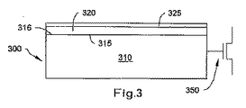
図3は、電界効果トランジスタ(FET)のゲートに連結されている参照電極300の断面図である。図3の参照電極300は、図2の参照電極200とほぼ同じであってよい。しかしながら図3の実施態様においては、参照電極300の導電性支持体310が、FETデバイス350のゲートに電気的に連結されている。図3ではFETデバイス350が示されているけれども、導電性支持体310は、必要に応じて、適切ないかなる電気デバイスもしくは電気回路にも連結することができる。導電性支持体310は、比較的高いインピーダンスインプットの電気デバイスもしくは電気回路に連結するのが好ましい。
FIG. 3 is a cross-sectional view of a
図4は、本発明のさらに他の実施態様による参照電極400の断面図である。参照電極400は導電性支持体410を含み、イオン絶縁性の疎水性層420が導電性支持体410に隣接して配置されている。非選択性イオン交換層425は、イオン絶縁性の疎水性層420上に配置された状態で、あるいはイオン絶縁性の疎水性層420に隣接した状態で示されている。
FIG. 4 is a cross-sectional view of a
本実施態様においては、導電性支持体410が誘電体層460上に配置されている。誘電体層460は、集積回路基板480〔あらかじめその中に形成されている素子(electronics)450を含む〕上に配置された状態で示されている。素子450は、参照電極400の導電性支持体410に電気的に相互連結すべく造られた1つ以上の導電性相互連結パッドを含んでよい。本実施態様においては、導電性支持体410と素子450の1つ以上の導電性相互連結パッドとを電気的に接続するために、VIA470が誘電体層460を貫いて形成されている。これらの素子を使用して、導電性支持体410からもたらされる基準電位を処理することができる(好ましくは、試験溶液中に配置されている1つ以上の電気化学センサーからもたらされる1つ以上の電気信号と組み合わせて)。
In this embodiment, a
図5は、本発明のさらに他の実施態様による参照電極500の断面図である。参照電極500は導電性支持体510を含む。このケースでは、導電性支持体510は半導体ウエハーである。イオン絶縁性の疎水性層520が、導電性支持体510の第1の表面515に隣接して設けられている。非選択性イオン交換層525を、イオン絶縁性の疎水性層520上に配置することができる。本実施態様においては、イオン絶縁性の疎水性層520と非選択性イオン交換層525が半導体ウエハーの裏面上に設けられている。
FIG. 5 is a cross-sectional view of a
図示のように、素子(electronics)550を半導体ウエハーの手前側に作製することができる。本実施態様においては、素子550がFETデバイスを含む。図からわかるように、FETデバイス550の支持体が、参照電極500の導電性支持体510に相当する。したがって、導電性支持体510上の基準電位がFETデバイス550の支持体にもたらされる。このようにして基準電位がもたらされる場合は、FETデバイス550のゲートを、試験溶液中に存在する電気化学センサーのアウトプットに接続することができる。この基準電位が、電気化学センサーからもたらされる所定のゲート電圧に対してFETデバイス550が供給する電流を相殺もしくは調整するのに役立つ。このような構造物は、電気変換器に良好な化学をもたらすのに役立つことがある。
As shown, an
実験のための集成体
以下の実施例は、試験装置を使用して試験した。この試験装置はpHセンサーであり、下記に説明するように設計・作製した。
Assembly for Experiments The following examples were tested using a test apparatus. This test apparatus is a pH sensor and was designed and manufactured as described below.
この試験装置においては、底部にOリングを取り付けたポリカーボネートチューブを、液密リザーバーを形成している標準的な3インチシリコンウエハーに突き当ててクランプ締めした。3インチシリコンウエハーを支持体として選択したのは、安価であり、入手が容易であり、市販の装置を使用して簡単に加工することができ、高度に制御された電気的特性と表面特性を有するからである。このウエハーをアルミニウム基板に当てて支持し、このときアルミニウム基板はさらに、ウエハーに対する電気接触を果たすための簡便な手段となった。調べようとするイオン絶縁性の疎水性材料をウエハーの上面にコーティングし、コーティングされた表面の電位を、標準的なpHプローブと二重連結のAg/AgCl基準プローブとに対して、オリオン(Orion)pHメーターによってモニターした。ストリップ・チャート・レコーダーによって出力を記録し、pHが4、6、8、および10の緩衝液を使用して安定性とドリフトをモニターした。
In this test apparatus, a polycarbonate tube with an O-ring attached to the bottom was abutted against a standard 3 inch silicon wafer forming a liquid tight reservoir and clamped. The choice of 3 inch silicon wafer as the support is inexpensive, readily available, and can be easily processed using commercially available equipment, providing highly controlled electrical and surface properties. It is because it has. The wafer was supported against the aluminum substrate. At this time, the aluminum substrate further became a simple means for achieving electrical contact with the wafer. An ion-insulating hydrophobic material to be investigated is coated on the top surface of the wafer, and the potential of the coated surface is compared to a standard pH probe and a doubly-coupled Ag / AgCl reference probe. ) Monitored by pH meter. The output was recorded by a strip chart recorder, and stability and drift were monitored using
材料の評価
本発明の方法を評価するために、パリレン(ポリ-p-キシレン)を含めた幾つかのサンプル材料を入手した。パリレンサンプル(“C”と“H”)は、パリレンの真空蒸着と他の絶縁保護コーティングを専門に扱っているスペシャルティ・コーティング・システムズ社(Specialty Coating Systems, Inc.)(ワイオミング州クリアレイク)から入手した。パリレン“C”(商用銘柄の標準的な材料)とパリレン“H”(吸水量がより少ないより高密度の材料)は、3インチシリコンウエハー(HTCから市販のウエハー)上の、ピンホールのない0.5μmフィルムとして得た。これらのフィルムを、パートIに記載の試験装置にて試験した。得られた結果を図6に示す。
Material Evaluation In order to evaluate the method of the present invention, several sample materials were obtained, including parylene (poly-p-xylene). Parylene samples ("C" and "H") are from Specialty Coating Systems, Inc. (Clear Lake, Wyoming), which specializes in parylene vacuum deposition and other insulating protective coatings. obtained. Parylene “C” (commercial grade standard material) and Parylene “H” (higher density material with less water absorption), no pinholes on 3 inch silicon wafer (wafers commercially available from HTC) Obtained as a 0.5 μm film. These films were tested with the test equipment described in Part I. The obtained results are shown in FIG.
図6における初期の結果は極めて良好に見える〔ほぼネルンスト様レスポンス(Nernstrian response)を示す〕けれども、フィルムは速やかに分解し始め、裸のシリコンのレスポンスに近づいていく。材料が極めて純粋な状態から真空蒸着されるので、ピンホールや連行不純物が欠陥を引き起こす恐れはないものと思われる。それどころか、これは、フィルムを通しての吸水とイオン電導の結果である。パリレンは、(全)吸水率の低い、周囲を被覆する厚いフィルムとして使用されるよう意図されている。この用途の場合、材料の最初の数ミクロンにおける水の侵入は取るに足りない量である。しかしながら我々のケースでは、全フィルム厚さは1μm未満であり、フィルム中へのごくわずかな吸水量が長期間にわたってある影響を及ぼす。グラフからわかるように、この影響は累積的であり、突然の不具合(たとえば、接着性の低下や表面からの剥がれ盛り上がり)よりむしろ、イオン伝導度が徐々に増大していることを示している。 Although the initial results in FIG. 6 look very good (substantially showing a Nernstrian response), the film begins to degrade rapidly and approaches the response of bare silicon. Since the material is vacuum deposited from a very pure state, pinholes and entrained impurities are unlikely to cause defects. On the contrary, this is a result of water absorption and ionic conduction through the film. Parylene is intended to be used as a thick film covering the periphery with a low (total) water absorption. For this application, water ingress in the first few microns of the material is insignificant. In our case, however, the total film thickness is less than 1 μm, and a very small amount of water absorption into the film has a long-term effect. As can be seen from the graph, this effect is cumulative, indicating a gradual increase in ionic conductivity rather than a sudden failure (eg, loss of adhesion or exudation from the surface).
テフロン(登録商標)AF
評価したもう一つの材料はテフロン(登録商標)AF(ポリ-テトラフルオロエチレン)であった。テフロン(登録商標)AF(1601S)のサンプルは、デュポン・フルオロプロダクツ社(デラウェア州ウィルミントン)から入手した。この材料は、FC-75(3M社から市販の過フッ化炭化水素溶媒)中6重量%溶液として入手した。次いで、自然酸化物を含んだウエハーを3000RPMにて30〜40秒スピンコーティングして、0.5〜1ミクロンの被膜を得た。コーティング後、ウエハーを160℃で少なくとも10分ベーキングして、過剰の溶媒を取り除き、ポリマーフィルムをキュアーした。フィルムの偏光解析により、平均厚さは約0.6μmであることが示され、屈折率は12.3であった(メーカーの規格と調和している)。
Teflon (registered trademark) AF
Another material evaluated was Teflon AF (poly-tetrafluoroethylene). Samples of Teflon AF (1601S) were obtained from DuPont Fluoro Products (Wilmington, Del.). This material was obtained as a 6 wt% solution in FC-75 (a fluorocarbon solvent commercially available from 3M). Next, the wafer containing the native oxide was spin-coated at 3000 RPM for 30-40 seconds to obtain a 0.5-1 micron film. After coating, the wafer was baked at 160 ° C. for at least 10 minutes to remove excess solvent and the polymer film was cured. Ellipsometry of the film showed an average thickness of about 0.6 μm and a refractive index of 12.3 (in line with the manufacturer's standards).
これらのフィルムは、フィルム面を横切るようにして指でこすることによって支持体から剥がすことができ、試験緩衝液と接触すると直ちに、余すところなく剥がれて盛り上がった。そこで、幾つかの表面調製法を検討した。 These films could be peeled from the support by rubbing with a finger across the film surface and immediately peeled and raised immediately upon contact with the test buffer. Therefore, several surface preparation methods were examined.
先ず、研磨したウエハーを160℃で1時間プレベーキングし、次いでFC75で湿潤して表面汚染物と吸着水を除去した。この結果、指でこすっても機械的に安定なフィルムが得られたが、水と接触すると、24〜48時間後にはまだ剥がれ盛り上りが生じた。ビーズ・ブラスティング(bead blasting)によって、次いでベーキングとウェッティングによって表面を機械的に粗くするように、我々は手順を変えた。ビーズ・ブラスティングしたウエハーは、機械的により安定であり、剥がれ盛り上がりによる不具合が起こる前に、数日間にわたって測定を行うことができた。 First, the polished wafer was pre-baked at 160 ° C. for 1 hour, and then wetted with FC75 to remove surface contaminants and adsorbed water. As a result, a mechanically stable film was obtained even when rubbed with a finger. However, when contacted with water, the film still peeled off after 24 to 48 hours. We changed the procedure to mechanically roughen the surface by bead blasting and then by baking and wetting. Bead-blasted wafers were more mechanically stable and could be measured over several days before failure due to flaking occurred.
我々はさらに、シロキサン〔ヘキサメチルジシロキサン(HMDS)〕を表面前処理剤として使用した。ビーズ・ブラスティングした(すなわち研磨した)ウエハーをHMDS蒸気に5分暴露し、次いで前述のように、直ちにFC-75で湿潤してスピンコーティングした。これらのフィルムは、ビーズ・ブラスティングしたウエハーに対しても、そして研磨したウエハーに対してもよく接着し、水と接触しても安定であった。 We further used siloxane [hexamethyldisiloxane (HMDS)] as a surface pretreatment agent. The bead blasted (ie polished) wafers were exposed to HMDS vapor for 5 minutes and then immediately wetted with FC-75 and spin coated as described above. These films adhered well to bead blasted wafers and to polished wafers and were stable when contacted with water.
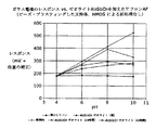
テフロン(登録商標)AF材料は極めて良好な基準レスポンス(reference response)を示す。表面前処理としてビーズ・ブラスティングだけを施したテフロン(登録商標)AFに対する典型的な結果を表7に示す。材料の初期レスポンスは極めて良好であり、直線性が強くほぼネルンスト様である、ということがわかる。我々のガラス電極は、標準的なAg/AgCl二重連結基準に対してネルンスト様であることが測定された。これに反して、シリコンだけがほぼフラットなレスポンスを示しており、ガラス電極の場合と同じ仕方でpHに応答しているという事実を表わしている。 Teflon AF material exhibits a very good reference response. Table 7 shows typical results for Teflon AF with only bead blasting as a surface pretreatment. It can be seen that the initial response of the material is very good, the linearity is strong and almost Nernst like. Our glass electrodes were measured to be Nernst-like against the standard Ag / AgCl double coupling standard. On the other hand, only silicon shows a nearly flat response, representing the fact that it responds to pH in the same way as with a glass electrode.
HMDSによる前処理を行って接着を促進させた場合の同じ材料を図8に示す。材料はほぼネルンスト様のレスポンスを示しており、21日間さらした後でも不具合の兆候は認められない。 FIG. 8 shows the same material when adhesion is promoted by pretreatment with HMDS. The material shows an almost Nernst-like response, with no signs of failure after 21 days of exposure.
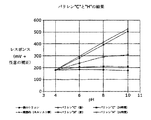
ゼオライトの改質
テフロン(登録商標)AF材料の表面イオン交換部位の密度を改良するために、ゼオライト・インタナショナル社(ペンシルバニア州バレーフォージ)から種々のゼオライトサンプルを入手した。CBV5524G(ロット番号1822-18)、CP814E(ロット番号1822-35)、CP814N、および単純なアルミナ(Al2Si2O7と表示する)。ベーキング前のまだ粘着性のあるテフロン(登録商標)上にゼオライト材料を振りかけ、これによって表面に機械的に埋め込むことによって、これらのゼオライト材料をテフロン(登録商標)表面に施した。ベーキング後、蒸留水を穏やかに流して、過剰のゼオライトを除去した。表面上にゼオライトを含んだフィルムは、そのままのテフロン(登録商標)AFより大幅に改良された挙動を示した。図9からわかるように、CBVグレード品とアルミナグレード品はほぼ同じ挙動を示した。
Various zeolite samples were obtained from Zeolite International (Valley Forge, PA) to improve the density of surface ion exchange sites in the modified Teflon AF material. CBV5524G (lot number 1822-18), CP814E (lot number 1822-35), CP814N, and simple alumina (designated as Al 2 Si 2 O 7 ). These zeolitic materials were applied to the Teflon surface by sprinkling the zeolitic materials on the still sticky Teflon before baking and thereby mechanically embedding the surface. After baking, distilled water was gently flushed to remove excess zeolite. Films containing zeolite on the surface showed significantly improved behavior over neat Teflon AF. As can be seen from FIG. 9, the CBV grade product and the alumina grade product showed almost the same behavior.
上記したそのままのテフロン(登録商標)と異なって、これらのフィルムは、新たに作製した場合でも、ややネルンスト様(sub-Nernstian)で非線形の挙動を明確に示す。数時間後、レスポンスは、“シリコン様”の挙動に向かって徐々に低下していく。この挙動は、自発的にプロトンを交換するアルミナやケイ酸塩の性質と矛盾しない。埋め込まれた材料は、フィルムの挙動に強い影響を及ぼす。このことは、ゼオライトを選択することで、フィルムの特性を造り上げることができる、ということを示している。 Unlike the neat Teflon® described above, these films clearly show a slightly Nernstian and non-linear behavior even when made fresh. After a few hours, the response gradually decreases towards a “silicon-like” behavior. This behavior is consistent with the nature of alumina and silicates that spontaneously exchange protons. The embedded material has a strong influence on the behavior of the film. This indicates that the properties of the film can be created by selecting zeolite.
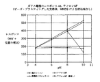
ロット番号1822グレードの材料は、アルミナより優れた基準特性(reference characteristics)を示す。CBV5524G(ロット番号1822-18)とCP814E(ロット番号1822-35)は、大きなアンモニウムイオンを収容するための内部キャビティを有するサイズ排除ゼオライト(size exclusion zeolytes)である。より小さなイオンはいずれもキャビティと自発的に交換され、化学的特性に対する優先傾向は認められない。これは、イオンの非特異性が重要となることがある参照電極に対するほぼ理想的なケースである。図10は、CP814E(ロット番号1822-35)に対する代表的な結果を示している。この場合も、テフロン(登録商標)AFだけの場合と同様に、レスポンスは極めて直線的である〔わずかに超ネルンスト様(super-Nernstian)ではあるが〕。 The lot number 1822 grade material exhibits reference characteristics superior to alumina. CBV5524G (lot number 1822-18) and CP814E (lot number 1822-35) are size exclusion zeolytes with internal cavities to accommodate large ammonium ions. Any smaller ions are spontaneously exchanged with the cavities, and no preference for chemical properties is observed. This is an almost ideal case for a reference electrode where ion non-specificity may be important. FIG. 10 shows representative results for CP814E (lot number 1822-35). Again, as with Teflon AF alone, the response is very linear (although slightly super-Nernstian).
ゼオライトCBV5524G(ロット番号1822-18)は、CP814E(ロット番号1822-35)よりやや小さい孔径を有する。したがって図11からわかるように、そのレスポンスはよりはっきりとややネルンスト様であり、孔径がより小さいことから、小さなイオンとプロトンの交換が幾らか優先的に起こっている。どちらの材料も、材料の接着が維持される限り、長期間(21日)にわたって極めて安定である。どちらの材料も、そのままのテフロン(登録商標)よりフィルムのレスポンス速度が大幅に向上し、イオン交換部位の密度が大きく増大することから、より小さなフィーチャー・サイズ(feature sizes)が可能となる。 Zeolite CBV5524G (lot number 1822-18) has a slightly smaller pore size than CP814E (lot number 1822-35). Thus, as can be seen from FIG. 11, the response is somewhat more Nernst-like and the pore size is smaller, so there is some preferential exchange of small ions and protons. Both materials are extremely stable over a long period (21 days) as long as the material adhesion is maintained. Both materials have significantly improved film response speeds compared to neat Teflon and the density of ion exchange sites is greatly increased, allowing for smaller feature sizes.
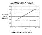
全イオン強度
試験溶液の全イオン強度に対するフィルムのレスポンスを調べるための実験を行った。フィルムが、試験溶液との非特異的なイオン交換の結果としてよりむしろ、表面の単純な空間電荷に基づいて“基準電位”を生成する場合、ゼロ点は、試験溶液の全イオン強度の変化と共に変わる。場合によっては、これは容認できない挙動となる。場の環境(field environment)のイオン強度が制御されていないからである。
An experiment was conducted to examine the response of the film to the total ionic strength of the total ionic strength test solution. If the film produces a “reference potential” based on a simple space charge on the surface, rather than as a result of non-specific ion exchange with the test solution, the zero point will be accompanied by a change in the total ionic strength of the test solution. change. In some cases this results in unacceptable behavior. This is because the ionic strength of the field environment is not controlled.
この挙動を調べるために、我々は、全イオン強度が1×10⁻⁴Mから1.0Mまで変化する溶液を試験した。試験溶液はKNO3の脱イオン水溶液(緩衝剤処理なし)であり、試験は室温で行った。ガラス電極のレスポンスと、標準的なAg/AgCl基準フィルムおよび試験フィルムとの関係を図12に示す。 To investigate this behavior, we tested solutions where the total ionic strength varied from 1 × 10 −4 M to 1.0M. The test solution was a deionized aqueous solution of KNO 3 (without buffer treatment), and the test was performed at room temperature. FIG. 12 shows the relationship between the response of the glass electrode and the standard Ag / AgCl reference film and test film.
溶液は緩衝剤処理されていないので、試験溶液のpHは、KNO3中の不純物や溶解CO2などと共に変化する。最大1Mの濃度において、イオン対形成(ion pairing)やこれに類似の現象はまだ重要なものとはなっていない、と我々は考える。したがって、ガラス電極のレスポンスの絶対値が溶液のpHに応じて変化する。しかしながら、2つのレスポンス間の差は一定であり、4 decades のイオン強度に対して5mV以下だけ変化する(1M濃度にて)。この挙動のために、フィルムのレスポンスのメカニズムにおいて、イオン強度に基づく表面の空間電荷形成は起こりそうもなく、我々は実際のところ、表面上の幾つかの部分と真のイオン交換があるものと考えている。 Since the solution is not buffered, the pH of the test solution varies with impurities in KNO 3 and dissolved CO 2 . We believe that at concentrations up to 1M, ion pairing and similar phenomena are not yet important. Therefore, the absolute value of the response of the glass electrode changes according to the pH of the solution. However, the difference between the two responses is constant and varies by no more than 5mV (at 1M concentration) for 4 decades of ionic strength. Because of this behavior, in the film response mechanism, space charge formation on the surface based on ionic strength is unlikely to occur, and we believe that there is in fact true ion exchange with some parts on the surface. thinking.
本発明は、上記の特定の実施例に限定されることはなく、添付の特許請求の範囲に記載の本発明の全ての態様を包含するものと理解しなければならない。本発明が適用可能な種々の改良形、同等のプロセス、および多くの構造物は、本明細書を見直せば当業者には明らかであろう。 It is to be understood that the invention is not limited to the specific embodiments described above, but encompasses all aspects of the invention as set forth in the appended claims. Various modifications, equivalent processes, and many structures to which the present invention is applicable will be apparent to those skilled in the art upon review of this specification.
Claims (39)
複数の非選択性イオン交換部位を有する、前記第1の表面に隣接したイオン絶縁性の疎水性層;
を含む参照電極。 A conductive support having a first surface; and an ion insulating hydrophobic layer adjacent to the first surface having a plurality of non-selective ion exchange sites;
Including a reference electrode.
前記第1の表面に隣接したイオン絶縁性の疎水性層;および
前記イオン絶縁性の疎水性層の上もしくは中に配置された非選択性イオン交換層;
を含む参照電極。 A conductive support having a first surface;
An ion insulating hydrophobic layer adjacent to the first surface; and a non-selective ion exchange layer disposed on or in the ion insulating hydrophobic layer;
Including a reference electrode.
前記第1の表面に隣接したイオン絶縁性の疎水性層;および
前記イオン絶縁性の疎水性層の上もしくは中に配置された非選択性イオン交換ゼオライト層;
を含む参照電極。 A conductive support having a first surface;
An ion insulating hydrophobic layer adjacent to the first surface; and a non-selective ion exchange zeolite layer disposed on or in the ion insulating hydrophobic layer;
Including a reference electrode.
複数の非選択性イオン交換部位を有する、前記第1の表面に隣接したイオン絶縁性の疎水性層;ならびに
ゲート、ソース、ドレイン、およびサブストレートを有する電界効果トランジスタ、前記導電性支持体が電界効果トランジスタのサブストレートに電気的に連結されている;
を含む参照電極。 A conductive support having a first surface;
An ion insulating hydrophobic layer adjacent to the first surface having a plurality of non-selective ion exchange sites; and a field effect transistor having a gate, source, drain, and substrate, wherein the conductive support is an electric field. Electrically connected to the substrate of the effect transistor;
Including a reference electrode.
Applications Claiming Priority (2)
| Application Number | Priority Date | Filing Date | Title |
|---|---|---|---|
| US10/681,440 US7318887B2 (en) | 2003-10-08 | 2003-10-08 | Solid state reference electrode |
| PCT/US2004/033016 WO2005036155A1 (en) | 2003-10-08 | 2004-10-08 | Solid state reference electrode |
Publications (2)
| Publication Number | Publication Date |
|---|---|
| JP2007508547A true JP2007508547A (en) | 2007-04-05 |
| JP2007508547A5 JP2007508547A5 (en) | 2007-07-26 |
Family
ID=34422282
Family Applications (1)
| Application Number | Title | Priority Date | Filing Date |
|---|---|---|---|
| JP2006534316A Ceased JP2007508547A (en) | 2003-10-08 | 2004-10-08 | Solid state reference electrode |
Country Status (4)
| Country | Link |
|---|---|
| US (1) | US7318887B2 (en) |
| EP (1) | EP1673617B1 (en) |
| JP (1) | JP2007508547A (en) |
| WO (1) | WO2005036155A1 (en) |
Families Citing this family (5)
| Publication number | Priority date | Publication date | Assignee | Title |
|---|---|---|---|---|
| US20070045128A1 (en) * | 2005-08-19 | 2007-03-01 | Honeywell International Inc. | Chlorine dioxide sensor |
| EP2469275B1 (en) | 2010-12-24 | 2015-12-23 | Honeywell Romania S.R.L. | Cantilevered carbon dioxide sensor |
| US10866208B2 (en) | 2018-09-21 | 2020-12-15 | Teralytic, Inc. | Extensible, multimodal sensor fusion platform for remote, proximal terrain sensing |
| US20220373542A1 (en) * | 2019-10-25 | 2022-11-24 | University Of Utah Research Foundation | Micro-Balance Biosensors to Detect Whole Viruses |
| CA3155252A1 (en) | 2021-04-09 | 2022-10-09 | National Research Council Of Canada | Glass-containing pseudo-reference electrode for use in ion-selective electrode sensors and ion selective field-effect transistors |
Family Cites Families (11)
| Publication number | Priority date | Publication date | Assignee | Title |
|---|---|---|---|---|
| US3926764A (en) * | 1971-05-19 | 1975-12-16 | Radiometer As | Electrode for potentiometric measurements |
| JPS5825221B2 (en) * | 1977-12-12 | 1983-05-26 | 株式会社クラレ | FET reference electrode |
| CA1228895A (en) | 1984-01-19 | 1987-11-03 | Imants R. Lauks | Ambient sensing devices |
| JPS60163419A (en) * | 1984-02-06 | 1985-08-26 | 東レ株式会社 | Deposited laminated film for capacitor |
| IT1229691B (en) * | 1989-04-21 | 1991-09-06 | Eniricerche Spa | SENSOR WITH ANTIGEN CHEMICALLY LINKED TO A SEMICONDUCTIVE DEVICE. |
| US5271820A (en) * | 1992-06-19 | 1993-12-21 | Monsanto Company | Solid state pH sensor |
| NO951705D0 (en) | 1995-05-03 | 1995-05-03 | Sinvent As | All-solid state reference electrode |
| US6094335A (en) * | 1998-10-09 | 2000-07-25 | Advanced Micro Devices, Inc. | Vertical parallel plate capacitor |
| US6483694B1 (en) * | 1999-06-22 | 2002-11-19 | Showa Denko Kabushiki Kaisha | Electrode for electrolytic capacitor, electrolytic capacitor, and manufacturing method therefor |
| US6426861B1 (en) * | 1999-06-22 | 2002-07-30 | Lithium Power Technologies, Inc. | High energy density metallized film capacitors and methods of manufacture thereof |
| US6793789B2 (en) * | 2000-09-30 | 2004-09-21 | Geun Sig Cha | Reference electrode with a polymeric reference electrode membrane |
-
2003
- 2003-10-08 US US10/681,440 patent/US7318887B2/en active Active
-
2004
- 2004-10-08 JP JP2006534316A patent/JP2007508547A/en not_active Ceased
- 2004-10-08 WO PCT/US2004/033016 patent/WO2005036155A1/en active Application Filing
- 2004-10-08 EP EP04794389.9A patent/EP1673617B1/en not_active Expired - Fee Related
Also Published As
| Publication number | Publication date |
|---|---|
| US20050077179A1 (en) | 2005-04-14 |
| EP1673617B1 (en) | 2018-04-11 |
| EP1673617A1 (en) | 2006-06-28 |
| US7318887B2 (en) | 2008-01-15 |
| WO2005036155A1 (en) | 2005-04-21 |
Similar Documents
| Publication | Publication Date | Title |
|---|---|---|
| Huang et al. | Improvement of integrated Ag/AgCl thin-film electrodes by KCl-gel coating for ISFET applications | |
| JP3588146B2 (en) | Ion-selective sensor and method of forming the same | |
| US3905889A (en) | Miniature multifunctional electrochemical sensor for simultaneous carbon dioxide-pH measurements | |
| JPH0633063U (en) | Graphite-based solid polymer membrane ion-selective electrode | |
| WO2008030582A2 (en) | Nanopore based ion-selective electrodes | |
| JP2017532571A (en) | Polymer electrode membrane | |
| US8394247B2 (en) | Anion concentration measuring device and anion concentration measuring element | |
| Kwon et al. | An all-solid-state reference electrode based on the layer-by-layer polymer coating | |
| EP0366566B1 (en) | Reference electrodes | |
| CN102980931A (en) | All-solid-state selective electrode based on functional ion liquid and preparation method of all-solid-state selective electrode | |
| Zine et al. | Hydrogen-selective microelectrodes based on silicon needles | |
| JP2007508547A (en) | Solid state reference electrode | |
| Teravaninthorn et al. | The suitability of Ta2O5 as a solid state ion-sensitive membrane | |
| Weng et al. | Enzymatic glucose biosensor based on TbYxOy electrolyte-insulator-semiconductor | |
| Chang et al. | Development of FET-type reference electrodes for pH-ISFET applications | |
| TWI637168B (en) | Method for preparing copper composite electrode and method for detecting histamine | |
| Iken et al. | Development of a Combined pH‐and Redox‐Sensitive Bi‐Electrode Glass Thin‐Film Sensor | |
| JP2009092647A (en) | Device and element for measuring anion concentration | |
| FR2624611A1 (en) | Homogeneous potentiometric sensor | |
| US10739303B2 (en) | Graphene-based sensor and method of fabricating same | |
| Pradel et al. | Chalcogenide glasses as sensitive membranes for the detection of ions in solution | |
| Darder et al. | Hybrid materials based on lichen–polysiloxane matrices: application as electrochemical sensors | |
| Arshak et al. | Drop-coated polyaniline composite conductimetric pH sensors | |
| Tomova et al. | Thin-film sensors based on evaporated chalcogenide glasses | |
| KR100434870B1 (en) | A composition for reference electrode membrane and reference electrode therewith |
Legal Events
| Date | Code | Title | Description |
|---|---|---|---|
| A521 | Written amendment |
Free format text: JAPANESE INTERMEDIATE CODE: A523 Effective date: 20070522 |
|
| A621 | Written request for application examination |
Free format text: JAPANESE INTERMEDIATE CODE: A621 Effective date: 20070522 |
|
| A01 | Written decision to grant a patent or to grant a registration (utility model) |
Free format text: JAPANESE INTERMEDIATE CODE: A01 Effective date: 20100225 |
|
| A977 | Report on retrieval |
Free format text: JAPANESE INTERMEDIATE CODE: A971007 Effective date: 20100225 |
|
| A045 | Written measure of dismissal of application [lapsed due to lack of payment] |
Free format text: JAPANESE INTERMEDIATE CODE: A045 Effective date: 20100617 |