JP2007501477A - Method and apparatus for determining access permissions - Google Patents
Method and apparatus for determining access permissions Download PDFInfo
- Publication number
- JP2007501477A JP2007501477A JP2006532516A JP2006532516A JP2007501477A JP 2007501477 A JP2007501477 A JP 2007501477A JP 2006532516 A JP2006532516 A JP 2006532516A JP 2006532516 A JP2006532516 A JP 2006532516A JP 2007501477 A JP2007501477 A JP 2007501477A
- Authority
- JP
- Japan
- Prior art keywords
- access
- master
- access permission
- information
- state information
- Prior art date
- Legal status (The legal status is an assumption and is not a legal conclusion. Google has not performed a legal analysis and makes no representation as to the accuracy of the status listed.)
- Pending
Links
Images


Classifications
-
- G—PHYSICS
- G06—COMPUTING; CALCULATING OR COUNTING
- G06F—ELECTRIC DIGITAL DATA PROCESSING
- G06F11/00—Error detection; Error correction; Monitoring
- G06F11/30—Monitoring
-
- G—PHYSICS
- G06—COMPUTING; CALCULATING OR COUNTING
- G06F—ELECTRIC DIGITAL DATA PROCESSING
- G06F21/00—Security arrangements for protecting computers, components thereof, programs or data against unauthorised activity
- G06F21/30—Authentication, i.e. establishing the identity or authorisation of security principals
- G06F21/31—User authentication
- G06F21/316—User authentication by observing the pattern of computer usage, e.g. typical user behaviour
-
- G—PHYSICS
- G06—COMPUTING; CALCULATING OR COUNTING
- G06F—ELECTRIC DIGITAL DATA PROCESSING
- G06F13/00—Interconnection of, or transfer of information or other signals between, memories, input/output devices or central processing units
- G06F13/14—Handling requests for interconnection or transfer
- G06F13/20—Handling requests for interconnection or transfer for access to input/output bus
- G06F13/28—Handling requests for interconnection or transfer for access to input/output bus using burst mode transfer, e.g. direct memory access DMA, cycle steal
-
- G—PHYSICS
- G06—COMPUTING; CALCULATING OR COUNTING
- G06F—ELECTRIC DIGITAL DATA PROCESSING
- G06F13/00—Interconnection of, or transfer of information or other signals between, memories, input/output devices or central processing units
- G06F13/14—Handling requests for interconnection or transfer
- G06F13/36—Handling requests for interconnection or transfer for access to common bus or bus system
-
- G—PHYSICS
- G06—COMPUTING; CALCULATING OR COUNTING
- G06F—ELECTRIC DIGITAL DATA PROCESSING
- G06F21/00—Security arrangements for protecting computers, components thereof, programs or data against unauthorised activity
- G06F21/60—Protecting data
- G06F21/62—Protecting access to data via a platform, e.g. using keys or access control rules
-
- G—PHYSICS
- G06—COMPUTING; CALCULATING OR COUNTING
- G06F—ELECTRIC DIGITAL DATA PROCESSING
- G06F21/00—Security arrangements for protecting computers, components thereof, programs or data against unauthorised activity
- G06F21/70—Protecting specific internal or peripheral components, in which the protection of a component leads to protection of the entire computer
- G06F21/78—Protecting specific internal or peripheral components, in which the protection of a component leads to protection of the entire computer to assure secure storage of data
-
- G—PHYSICS
- G06—COMPUTING; CALCULATING OR COUNTING
- G06F—ELECTRIC DIGITAL DATA PROCESSING
- G06F21/00—Security arrangements for protecting computers, components thereof, programs or data against unauthorised activity
- G06F21/70—Protecting specific internal or peripheral components, in which the protection of a component leads to protection of the entire computer
- G06F21/82—Protecting input, output or interconnection devices
-
- H—ELECTRICITY
- H04—ELECTRIC COMMUNICATION TECHNIQUE
- H04L—TRANSMISSION OF DIGITAL INFORMATION, e.g. TELEGRAPHIC COMMUNICATION
- H04L9/00—Cryptographic mechanisms or cryptographic arrangements for secret or secure communications; Network security protocols
Abstract
複数のマスタ(12,14)に対応する複数のアクセス要求(84)を受信するステップと、アクセス許可(86)を決定するステップと、状態情報(60)を提供するステップと、アクセス要求(84)に基づいてアクセス許可(86)を決定ステップと、状態情報(90)に基づいてアクセス許可を選択的に修正するステップと、を含むアクセス保護(96)を決定するための方法および装置。状態情報(60)は、デバッグ動作、非セキュアまたは検証されていないメモリからの動作、メモリ・プログラミング、ダイレクト・メモリ・アクセス動作、ブート動作、ソフトウェア・セキュリティ検査、セキュリティ・レベル、セキュリティ監視動作、動作モード、障害監視装置、外部バス・インタフェース等(88)と関連することができる。 Receiving a plurality of access requests (84) corresponding to a plurality of masters (12, 14); determining an access permission (86); providing status information (60); and an access request (84). And determining the access protection (96) based on the status information (90) and selectively modifying the access permission (96). State information (60) includes debug operations, operations from non-secure or unverified memory, memory programming, direct memory access operations, boot operations, software security checks, security levels, security monitoring operations, operations Mode, fault monitor, external bus interface, etc. (88).
Description
本発明は、アクセス許可に関し、特に、例えば、データ処理システムでアクセス許可を決定するためのアクセス許可回路に関する。 The present invention relates to access permission, and more particularly to an access permission circuit for determining access permission in a data processing system, for example.
システム・オン・チップ(SoC)法の場合には、通常、例えば、メモリのような共有周辺部品およびスレーブ・デバイスを含む複数のマスタが存在する。共有周辺部品およびスレーブ・デバイスのすべてまたはいくつかのコンテンツは、システムを破壊する恐れがあるいくつかのマスタ上で稼働している、正当でないまたはその他の悪意のあるソフトウェアによる不正な変更、複写または問合せから保護しなければならない場合がある。例えば、システムの周辺デバイスおよびスレーブ・デバイス内のセキュア情報にアクセスするために使用することができる、安全保護されていないマスタ上で稼働しているソフトウェアにより、ウイルスが侵入する場合がある。さらに、システム内のいくつかのバス・マスタには安全保護されていると見なせるものもあるし、見なせないものもある。これらの状態は、システムの状態が変化すると変化する場合がある。 In the case of a system on chip (SoC) method, there are typically multiple masters including shared peripheral components such as memory and slave devices. All or some content of shared peripherals and slave devices may be tampered with, altered or copied by unauthorized or other malicious software running on some masters that could destroy the system You may need to protect against queries. For example, a virus may be invaded by software running on an unsecured master that can be used to access secure information in the peripheral and slave devices of the system. In addition, some bus masters in the system may or may not be considered secure. These states may change as the state of the system changes.
それ故、システムの統合性およびセキュリティを確保するために、安全保護されていないマスタ上で稼働している正当でないまたは他の悪意のあるソフトウェアからシステムを保護する必要がある。 Therefore, in order to ensure system integrity and security, there is a need to protect the system from unauthorized or other malicious software running on an unsecured master.
添付の図面に本発明を示すが、これは例示としてのものであって本発明を制限するものではない。図面中、類似の参照番号は類似の要素を示す。
当業者であれば、図面中の要素は図面を見やすく、分かりやすくするためのものであって、必ずしも正確な縮尺によるものではないことを理解することができるだろう。例えば、本発明の実施形態の理解を助けるために、図の要素のうちのあるものの寸法は他の要素より誇張してある場合がある。
The present invention is illustrated in the accompanying drawings, which are intended to be illustrative and not limiting. In the drawings, like reference numbers indicate like elements.
Those skilled in the art will appreciate that the elements in the drawings are for ease of viewing and understanding and are not necessarily to scale. For example, to assist in understanding embodiments of the present invention, the dimensions of some of the elements in the figures may be exaggerated over other elements.
本明細書で使用する場合、「バス」という用語は、データ、アドレス、制御または状態のような1つ以上の種々のタイプの情報を転送するのに使用することができる複数の信号または導体を指すために使用される。本明細書で使用する導体は、1本の導体、複数の導体、一方向導体、または二方向導体に関連して説明または記述することができる。しかし、他の実施形態の場合には、異なる導体を使用することができる。例えば、二方向導体の代わりに別々の一方向導体を使用することもできるし、その逆を行うこともできる。また、複数の導体の代わりに、直列にまたは時間多重により複数の信号を転送する1本の導体を使用することができる。同様に、複数の信号を運ぶ1本の導体を、これら信号のサブセットを運ぶ種々の異なる導体に分割することもできる。それ故、信号を転送するのに多くの任意の方法を使用することができる。 As used herein, the term “bus” refers to a plurality of signals or conductors that can be used to transfer one or more different types of information, such as data, address, control or status. Used to point. As used herein, a conductor can be described or described in connection with a single conductor, multiple conductors, one-way conductor, or two-way conductor. However, in other embodiments, different conductors can be used. For example, separate unidirectional conductors can be used instead of bidirectional conductors and vice versa. Further, instead of a plurality of conductors, a single conductor that transfers a plurality of signals in series or by time multiplexing can be used. Similarly, a single conductor carrying multiple signals can be divided into a variety of different conductors carrying a subset of these signals. Therefore, many arbitrary methods can be used to transfer the signal.
システムの統合性およびセキュリティを確保するためには、例えば、複数のマスタ・データ処理システムのようなシステムが、安全保護されていないプロセッサまたは他のマスタ上で稼働している正当でないまたは他の悪意のあるソフトウェアにより決して危険にさらされないようにすることが望ましい。例えば、複数のマスタ・システム内の複数のマスタは、例えば、システムの周辺デバイスまたはスレーブ・デバイスのような同じリソースを共有することができる。複数のマスタのうちのいくつかは安全保護されていると見なす
ことができるが、他のものは安全保護されていないと見なすことができる。本明細書で使用する場合には、セキュア・マスタという用語は、一般的によりアクセスし易く、損傷を受けやすい非セキュア・マスタに比べて、一般的にアクセスしにくく、損傷を受けにくいマスタを意味する。例えば、セキュア・マスタは、アクセスしにくく、またはマスタまたはSoCのメーカーにより完全に制御されている命令を実行することができる(すなわち、セキュア・マスタ上で稼働しているソフトウェアは、信頼性の高いソフトウェアまたはセキュア・ソフトウェアであると見なすことができる)。しかし、非セキュア・マスタは、第三者ソフトウェア(例えば、ユーザが開発したソフトウェア)を受信し、実行することができる一般的な用途向けのプロセッサであってもよいし、または任意の他の信頼できないソフトウェア(一般的に、ソフトウェアの内容および機能が分からない)であってもよい。ソフトウェアが信頼できないので、そのソフトウェアは、システムの他の部分を破壊しようとするかもしれないし、またはセキュア情報にアクセスしようとするかもしれない、正当でないかまたは他の悪意のあるソフトウェアである場合がある。さらに、安全保護されている、または安全保護されていない特定のマスタの状態は、データ処理システムが変化すると変化する場合がある。
In order to ensure system integrity and security, for example, a system such as multiple master data processing systems may not be legitimate or otherwise malicious when running on an unsecured processor or other master. It is desirable to never be compromised by existing software. For example, multiple masters in multiple master systems can share the same resources, such as, for example, peripheral devices or slave devices of the system. Some of the multiple masters can be considered secure, while others can be considered unsecured. As used herein, the term secure master refers to a master that is generally less accessible and less susceptible to damage than a non-secure master that is generally more accessible and susceptible to damage. To do. For example, a secure master is difficult to access or can execute instructions that are fully controlled by the master or SoC manufacturer (ie, software running on the secure master is reliable) Can be considered software or secure software). However, the non-secure master may be a general purpose processor that can receive and execute third party software (eg, software developed by a user) or any other trust Software that cannot be used (generally, the contents and functions of the software are not known). Because the software is untrustworthy, it may be legitimate or other malicious software that may attempt to destroy other parts of the system or access secure information. is there. Further, the state of a particular master that is secured or not secured may change as the data processing system changes.
それ故、本発明の一実施形態を使用すれば、例えば、不揮発性メモリのようなスレーブ・デバイスまたは周辺デバイスの内容を安全保護されている状態で動作している場合、プログラムの実行を、不揮発性メモリから続行することができるが、もっと安全保護の薄い状態で動作している場合に、不正なアクセスを防止することができる方法で安全保護状態にすることができる。一実施形態は、システム状態が図1〜図3を参照しながら以下に説明するように、データ処理システムの予めプログラムしたアクセス保護政策を修正または無視することができる方法を提供する。上記無視は、例えば、システムのリソース(例えば、スレーブ・デバイス、周辺デバイス、メモリ、共有リソース等)へのシステム内の各マスタに対して、一緒にまたは別々に、読出しアクセスおよび書込アクセスを制限するために(または逆にこれらのアクセスに対するアクセス許可を緩やかにするために)使用することができる。さらに、これらの無視は、状態情報が変化すると、動的に変化する場合がある。また、さらに以下に説明するように、状態情報は、例えば、デバッグ・モードを使用できるようにすること、安全保護されていないまたは検証されていないメモリ領域からのプログラムの実行、不揮発性メモリの一部の再プログラミング等に関連する情報のようなデータ処理システムの状態に関する任意のタイプの情報を含むことができる。 Therefore, using an embodiment of the present invention, for example, when operating in a state where the contents of a slave device or peripheral device such as a nonvolatile memory are secured, Can continue from the memory, but when operating in a less secure state, it can be put into a secure state in a way that can prevent unauthorized access. One embodiment provides a method in which the system state can modify or ignore the pre-programmed access protection policy of the data processing system, as described below with reference to FIGS. The above ignores, for example, restrict read and write access, either together or separately, to each master in the system to system resources (eg, slave devices, peripheral devices, memory, shared resources, etc.) (Or vice versa to loosen access permissions for these accesses). Furthermore, these ignores may change dynamically as the state information changes. In addition, as will be described further below, status information may include, for example, enabling use of debug mode, executing a program from a memory area that is not secure or not verified, and a non-volatile memory. Any type of information regarding the state of the data processing system, such as information related to part reprogramming, may be included.
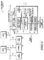
図1は、データ処理システム10の一実施形態である。データ処理システム10は、マスタ12(相互接続またはバス・マスタ12とも呼ばれる)と、マスタ14(相互接続またはバス・マスタ14とも呼ばれる)と、メモリ・コントローラ32と、不揮発性メモリ36と、システム相互接続22と、1/O回路16と、周辺デバイス18と、他のスレーブ・デバイス20とを含む。マスタ12は、導体48を通してシステム相互接続22に二方向で結合していて、マスタ14は、導体50を通してシステム相互接続22に二方向で結合していて、I/O回路は、導体52を介してシステム相互接続22に二方向で結合していて、周辺デバイス18は、導体54を通してシステム相互接続22に二方向で結合していて、他のスレーブ・デバイス20は、導体56を通してシステム相互接続22に二方向で結合していて、メモリ・コントローラ32は、導体24を通してシステム相互接続22に二方向で結合している。導体24は、マスタ識別子26、アドレス/データ30、R/W信号28、および他の信号34を送るための導体を含む。
FIG. 1 is an embodiment of a
メモリ・コントローラ32は、アクセス保護制御レジスタ38と、アクセス修正回路40と、アクセス制御回路42と、メモリ・アクセス回路44とを含み、導体46を通して不揮発性メモリ36に二方向で結合している。アクセス保護制御レジスタは、アクセス修正回路40へアクセス許可58を提供する。アクセス修正回路40は、データ処理システ
ム10内の情報から導体62を通して、またメモリ・コントローラ32内の情報から導体64を通して状態情報60を受信し、修正したアクセス許可66をアクセス制御回路42に供給する。他の実施形態の場合には、状態情報60は、(導体62を通して)データ処理システム10が供給した情報だけを含むことができるか、またはメモリ・コントローラ32内から供給した情報だけを含むことができることに留意されたい。さらに、状態情報60は、(導体62の何本かのまたはすべてを介して)データ処理システム10の外部のソースから供給された情報を含むことができる。それ故、以下にさらに詳細に説明するように、状態情報60は、アクセス修正回路40に所望の状態情報を提供する任意のタイプの信号またはインジケータを含むことができる。アクセス制御回路42は、メモリ・アクセス回路44にアクセス許可インジケータ68(1つまたは複数のインジケータを含むことができる)を提供する。
The
図1には周辺デバイス18は1つしか図示していないが、データ処理システム10は、システム相互接続22と結合している任意の数の周辺デバイスを含むことができる。同様に、任意の数のマスタおよびスレーブをシステム相互接続22に結合することができ、図1に示すものに限定されない。また、一実施形態の場合には、すべてのデータ処理システム10を、1つの集積回路上または同じデバイス内に位置させることができることに留意されたい。別の方法としては、データ処理システム10は、任意の数の個々の集積回路または相互に接続している個々のデバイスを含むことができる。例えば、一実施形態の場合には、メモリおよびメモリ・コントローラ(例えば、不揮発性メモリ36およびメモリ・コントローラ32など)をデータ処理システム10の残りの部分から独立している1つまたは複数の集積回路上に位置させることができる。
Although only one
一実施形態の場合には、マスタ12およびマスタ14は、マイクロプロセッサ、デジタル信号プロセッサ等のような命令を実行することができるプロセッサであってもよいし、またはダイレクト・メモリ・アクセス(DMA)回路またはデバッグ回路のような任意の他のタイプの相互接続またはバス・マスタを含むことができる。また、図には2つのマスタしか図示していないが、データ処理システム10は、必要に応じて任意の数(1つまたは複数)のマスタを含むことができる。また、任意の所与の動作点において、各マスタ12および14は、異なるレベルのセキュリティを行うことができることに留意されたい。すなわち、例えば、特定の動作点におけるデータ処理システム10の状態に従って、各マスタ12および14は、安全保護されているマスタであってもよいし、安全保護されていないマスタであってもよい。周辺デバイス18は、汎用非同期受信送信機(UART)、リアルタイム・クロック(RTC)、キーボード・コントローラ、任意のタイプのメモリ等のような任意のタイプの周辺デバイスであってもよい。他のスレーブ20が、例えば、マスタ12および14がアクセスすることができるメモリ、および周辺デバイス18のような同じタイプの周辺デバイスを含むシステム・バス上に常駐する任意のタイプの周辺デバイスのような任意のタイプの相互接続スレーブを含むことができることに留意されたい。I/O回路16は、データ処理システム10の内部または外部の情報を受信し、提供する任意のタイプのI/O回路を含むことができる。
In one embodiment,
図の実施形態の場合には、メモリ・コントローラ32および不揮発性メモリ36は、システム相互接続22と結合している他のスレーブ・デバイスに対応する。一実施形態の場合には、不揮発性メモリ36を、システム相互接続22(例えば、マスタ12および14など)と結合している少なくとも2つのマスタにより共有することができることに留意されたい。不揮発性メモリ36は、マスタ12および14として同じ集積回路上に、または別々の集積回路上に位置させることができる。さらに、図のメモリ36は、不揮発性メモリ(フラッシュ・メモリなど)であるが、メモリ36は、例えば、読出し専用メモリ(ROM)、ランダム・アクセス・メモリ(RAM)、ダイナミックRAM(DRAM)、スタティックRAM(SRAM)、不揮発性メモリ(例えば、フラッシュ、MRAM)等の
ような任意のタイプのメモリであってもよい。また、メモリ36は、他の周辺デバイスまたはスレーブ・デバイス内に位置するメモリまたは他の記憶装置であってもよい。さらに他の実施形態の場合には、メモリ36は、メモリ・コントローラ32を、リソースを保護するためのアクセス保護回路を有する任意のタイプのコントローラと置換できる場合に、保護する必要があるセキュア情報を有する任意の他のタイプのリソースであってもよい。
In the illustrated embodiment,
システム相互接続22は、マスタ12、マスタ14、I/O回路16、周辺デバイス18、他のスレーブ・デバイス20、およびメモリ・コントローラ32を相互に接続する。一実施形態の場合には、図1に示すように、システム相互接続22は、システム・バス・プロトコルにより動作するシステム・バスとして実施される。別の方法としては、システム相互接続22を、例えば、種々のデバイス間で情報を経路指定するスイッチング回路のような相互接続回路により実施することができる。
The
動作中、マスタ12および14は、メモリ・コントローラ32を介して、他のスレーブ・デバイス20、周辺デバイス18、または不揮発性メモリ36へのアクセスを要求するために、システム相互接続22の使用を要求する。要求を行っているマスタは、システム相互接続22を介して、メモリ・コントローラ32にアクセス要求を供給することができる。アクセス要求は、例えば、データまたは命令に対する読出し要求または書込み要求であってもよい。メモリ・コントローラ32は、読出しアクセス要求に応じて、要求しているマスタが十分なアクセス許可を有しているものと仮定して、システム相互接続22を介して要求しているマスタに要求された情報(データまたは命令)を返送する。一実施形態の場合には、アクセス要求に対して、マスタ識別子26がメモリ・コントローラ32に提供され、メモリ・コントローラはどのマスタが現在のアクセスを要求しているのかを識別する。また、現在のアクセス要求が読出しタイプのアクセスなのか、書込みタイプのアクセスなのかを表示するために、R/W信号28をメモリ・コントローラ32に提供することもできる。メモリ・コントローラ32は、また、現在のアクセス要求に対応するアドレス情報を受信し、アドレス/データ30により要求された情報を提供する。メモリ・コントローラ32へ/から送らなければならない任意の他の信号(状況、制御、データなど)は、他の信号34により提供することができる。
In operation,
マスタ12および14のような各マスタは、不揮発性メモリ36への特定のアクセス要求が許可できるものかどうかを判断するために使用することができる、対応するアクセス許可を有することができる。例えば、特定のマスタは、不揮発性メモリ36に対する書込みアクセスまたは読出しアクセスに対する異なるアクセス許可を有することができる。一実施形態の場合には、これらのアクセス許可は、アクセス保護制御レジスタ38内に記憶される。
Each master, such as
図2は、図1のアクセス保護制御レジスタ38の一例である。一実施形態の場合には、アクセス保護制御レジスタ38は、データ処理システム10内の各マスタに対する1つのアクセス保護フィールドを含む。例えば、アクセス保護制御レジスタ38は、それぞれマスタ12および14に対応するマスタ12アクセス保護フィールド70およびマスタ14アクセス保護フィールド76を含む。アクセス保護フィールドは、特定のマスタにより不揮発性メモリ36への特定のタイプのアクセスが許可されるかどうかを表示する。例えば、図の実施形態の場合には、各アクセス保護フィールド70および76は、各マスタに対する読出しアクセスおよび書込みアクセスに対する許可を表示するために、読出しアクセス保護フィールドおよび書込アクセス保護フィールドを含む。
FIG. 2 is an example of the access protection control register 38 of FIG. In one embodiment, the access protection control register 38 includes one access protection field for each master in the
マスタ12アクセス保護フィールド70は、マスタ12が、不揮発性メモリ36に読出しアクセスを行うことができるかどうかを表示する、マスタ12読出しアクセス保護フィールド72、およびマスタ12が、不揮発性メモリ36に書込みアクセスを行うことがで
きるかどうかを表示する、マスタ12書込みアクセス保護フィールド74を含む。それ故、マスタ12は、不揮発性メモリ36に読出しアクセス、または書込みアクセスの一方だけを行うことを許可することができる。別の方法としては、マスタ12は、フィールド72および74の値に従って、不揮発性メモリ36への読出しおよび書込みアクセスの両方を行うことを許可することもできるし、読出しアクセスおよび書込みアクセスの両方を行うことを許可しないこともできる。一実施形態の場合には、各フィールド72および74は、対応するアクセス・タイプ(読出しまたは書込み)が許可されるかどうかを示すための1ビット・フィールドである。同様に、マスタ14アクセス保護フィールド76は、マスタ14が、不揮発性メモリ36へ読出しアクセスを行うことができるかどうかを示すマスタ14読出しアクセス保護フィールド78、マスタ14が、不揮発性メモリ36に対して書込みアクセスを行うことができるかどうかを示すマスタ14書込みアクセス保護フィールド80を含む。それ故、マスタ14は、不揮発性メモリ36への読出しアクセス、または書込みアクセスの一方だけを行うことを許可することができる。別の方法としては、マスタ14は、フィールド78および80の値に従って、不揮発性メモリ36への読出しおよび書込みアクセスの両方を行うことを許可することもできるし、読出しアクセスおよび書込みアクセスの両方を行うことを許可しないこともできる。一実施形態の場合には、各フィールド78および80は、対応するアクセス・タイプ(読出しまたは書込み)が許可されるかどうかを示すための1ビット・フィールドである。
The
他の実施形態の場合には、アクセス保護制御レジスタ38は、フィールド70および76のような任意の数のアクセス保護フィールドを含むことができることに留意されたい。例えば、アクセス保護制御レジスタ38は、データ処理システム10内の各マスタに対する1つのアクセス保護フィールドを含むこともできるし、データ処理システム10内にマスタのサブセットだけを含むこともできる。また、各アクセス保護フィールド70および76は、読出しおよび書込みアクセス(例えば、バースト・アクセスなど)の代わりにまたはそれに加えて、異なるタイプのアクセスに基づいて、許可を識別するための任意の数のフィールドを含むことができることに留意されたい。さらに、フィールド70、72、74、76、78、および80は、異なるフィールド定義、異なるビット割当て、または異なる数のビットを使用するというような種々の異なる方法で実施することができる。別の方法としては、これらのフィールドは、またはデータ処理システム10の別々のレジスタまたは他のレジスタまたはメモリ位置のような異なる方法で組織化することができる。通常、アクセス保護制御レジスタ38は、セキュア・マスタによりプログラムすることができるソフトウェアである。一実施形態の場合には、アクセス保護制御レジスタ38は、リセットの際にプログラムすることができる。
Note that in other embodiments, the access protection control register 38 may include any number of access protection fields, such as
図1に戻って説明すると、アクセス修正回路40は、制御レジスタ38内に記憶しているアクセス許可の1つまたは複数を修正(または無視)するために使用することができる。例えば、状態情報60に従って、アクセス修正回路40は、修正したアクセス許可66を提供するために、アクセス保護制御レジスタ38からアクセス許可58を選択的に修正することができる。すなわち、場合によっては、修正したアクセス許可66を生成するために、すべてのアクセス許可58を修正することができるし、または別の方法としては、修正したアクセス許可66が1つだけまたはいくつかの修正した許可を含むように、アクセス許可58の1つだけまたはいくつかを修正することができる。すなわち、修正したアクセス許可66は、現在修正されていないアクセス保護制御レジスタ38からの許可を含むことができる。また、修正したアクセス許可66は、特定のマスタに対してメモリ36へのもっと広い(または制限がもっと緩やかな)アクセスを供給することができし、または特定のマスタに対してメモリ36へのアクセスを制限することもできることに留意されたい。
Returning to FIG. 1, the
図1に戻って説明すると、アクセス制御回路42は、修正したアクセス許可66に基づ
いて、現在のアクセス要求が許可されるかどうかを判断することができる。例えば、データ処理システム10内の各マスタ(マスタ12および14など)は、対応するマスタ識別子を有することができる。一実施形態の場合には、各マスタを対応する番号により一意に識別することができるように、マスタ12をマスタ識別子0に対応させることができるし、マスタ14をマスタ識別子1に対応させることができる。他の実施形態の場合には、任意のタイプの識別子を使用することができ、任意の方法で割り当てることができ、0からスタートするまたは1桁の番号からスタートするというような番号順に制限されない。また、他の実施形態の場合には、複数のマスタが同じマスタ識別子を共有することができる。それ故、アクセス制御回路42は、(マスタ識別子26によりアクセス制御回路42に表示された)現在のアクセスをどのマスタが要求しているのかに基づいて、また(修正したアクセス許可66によりアクセス制御回路42に表示された)アクセス許可に基づいて、不揮発性メモリ36へのアクセスが許可されるかどうかを判断することができる。アクセスが許可される場合には、アクセス許可インジケータ68が、メモリ・アクセス回路44が、要求したアクセスを終了(例えば、要求した読出しまたは書込みを終了)するために必要な信号および情報を不揮発性メモリ36に供給することができるように、メモリ・アクセス回路44へのアクセスが許可されることを表示する。しかし、現在要求しているマスタに対する修正したアクセス許可66に基づいて、アクセス制御回路42が、アクセスが許可されないと判断した場合には、アクセス許可インジケータ68は、メモリ・アクセス回路44が要求したアクセスを終了しないように、アクセスが許可されないことを表示する。図3を参照しながら、メモリ・コントローラ32の動作についてさらに説明する。
Returning to FIG. 1, the
図3は、本発明の一実施形態によるメモリ・コントローラ32の動作に対応する流れ96を示す。流れ96は、スタート82からスタートし、ブロック84に進み、ここでアクセス要求が受信される。例えば、マスタ12または14は、システム相互接続22を介して、不揮発性メモリ36にアクセス要求を供給することができる。アクセス要求は、例えば、R/W信号28で示すように、読出し要求または書込み要求であってもよい。次に、流れはブロック86に進み、ここでアクセス許可が決定される。例えば、これらのアクセス許可は、アクセス保護制御レジスタ38内のフィールド(フィールド70および76など)により提供することができる。次に、流れはブロック88に進み、ここで状態情報(状態情報60など)が受信される。状態情報は、例えば、デバッグ動作、安全保護されていないまたは検証されていないメモリからの動作、メモリ・プログラミング、ダイレクト・メモリ・アクセス(DMA)動作、ブート動作、ソフトウェア・セキュリティ検査、セキュリティ・レベル、セキュリティ監視動作、動作モード、障害監視装置、外部バス動作等と関連することができる。すなわち、情報は、状態情報60により、上記条件、状態または動作の1つまたは複数を表示することができるアクセス修正回路40に提供することもできるし、上記条件、状態または動作の1つまたは複数に関連する情報を表示することもできる。それ故、状態情報60は、メモリ・コントローラ32内の(マスタ12、マスタ14、I/O回路16、周辺デバイス18または他のスレーブ20からのような)データ処理システム10内の種々の場所から、またはデータ処理システム10の外部の場所から、またはこれらの任意の組合わせから受信することができる。
FIG. 3 illustrates a
例えば、デバッグ動作に関連する状態情報の場合には、状態情報60の信号の1つまたは複数を、別々のユニットとしての、または例えば、マスタ12または14の一部としてのシステム相互接続22と結合しているデバッグ回路(図示せず)から受信することができる。状態情報60内の信号は、また、アクセス修正回路40への2つ以上のリソースに基づいて、結合状態情報または状態情報を提供するための種々の異なる方法で結合することができる。この結合回路は、アクセス修正回路40内、アクセス修正回路40の外部、またはメモリ・コントローラ32の外部にも位置することができる。
For example, in the case of state information related to debug operations, one or more of the signals of
図3を参照すると、次に、流れはブロック90に進み、ここで受信した状態情報に基づいて、アクセス許可が選択的に修正される。例えば、一実施形態の場合には、状態情報60により送られたいくつかの条件または状況が、アクセス保護制御レジスタ38内に記憶している許可を、ハードウェアにより無視することができるように、アクセス許可を修正するためにハードウェア無視を使用することができる。例えば、一実施形態の場合には、いくつかの条件が満たされた場合に、修正したアクセス許可66のような修正したアクセス許可を生成するために、ハードウェアによりアクセス保護制御レジスタ38の値を修正または置換できるように、状態情報60を必要に応じて結合し、ハードウェア無視回路に入力(または直接入力)することができる。別の方法としては、修正したアクセス許可66を生成するために、他のハードウェア的方法またはソフトウェア的方法のような他の方法で状態情報60に基づいて、アクセス許可58を選択的に修正することができる。
Referring now to FIG. 3, the flow then proceeds to block 90 where access permissions are selectively modified based on the received status information. For example, in one embodiment, the permission stored in the access protection control register 38 by some conditions or status sent by the
次に、流れは、ブロック92に進み、ここで修正したアクセス許可に基づいて、要求したアクセスが選択的に実行される。例えば、マスタ12が不揮発性メモリ36に読出しアクセスを要求し、マスタ12の読出しアクセス保護フィールド72が、マスタ12による読出しアクセスが許可されることを表示した場合には、(それがアクセス修正回路40により修正されていないと仮定して)マスタ12の要求が実行される。しかし、状態情報60が、マスタ12の読出しアクセス許可を(許可ではなく拒否するように)修正すべきであると表示している場合には、要求した読出しアクセスが許可ではなく、拒否され、マスタ12読出しアクセス保護フィールド72を無視するように、アクセス修正回路40は、読出しアクセス許可を修正する(およびそれを修正したアクセス許可66の一部として提供する)ことができる。次に、流れはエンド94のところで終わる。(図3の流れは、メモリ・コントローラ32を介して、メモリ36への各アクセス要求の度に反復することができることに留意されたい。)
それ故、マスタ12または14のようなマスタによる不揮発性メモリ36への各アクセスの場合、アクセス保護制御レジスタ38は、現在のアクセスを許可すべきかどうかを判断するために使用することができるアクセス許可58を提供する。しかし、データ処理システム10の状態情報に従って、これらソフトウェア・プログラマブル・レジスタを無視するのが望ましい(それ故、修正したアクセス許可66になる)状況がある。例えば、アクセス保護制御レジスタ38がソフトウェア・プログラマブルである場合には、アクセス保護制御レジスタ38内に記憶している許可が、非セキュア・ソフトウェアにより、保護しなければならないセキュア情報へのアクセスを間違って許可するように変化している場合がある。それ故、データ処理システム10のある状態情報または条件に従って、セキュア情報へのアクセスを防止するために、アクセス保護制御レジスタ38のアクセス許可を修正するために使用することができる修正(ハードウェア無視など)を行うために、アクセス修正回路40を使用することができる。
The flow then proceeds to block 92 where the requested access is selectively performed based on the modified access permissions. For example, if the
Therefore, for each access to the
ある例の場合には、デバッグ動作中アクセスを制限しなければならない場合がある。何故なら、デバッグ中は、一般的に、データ処理システム10にアクセスし易くなるからである。それ故、一実施形態の場合には、状態情報60は、デバッグを行うことができる時を表示するデバッグ回路(図示せず)からの情報を含む。この場合、アクセス保護制御レジスタ38内に記憶しているマスタ12および14のうちのいくつかまたはすべての許可をアクセス修正回路40により修正することができる。
In some cases, access may need to be restricted during debugging operations. This is because it is generally easy to access the
他の例の場合には、非セキュアまたは検証されていないメモリからの動作中、データ処理システム10のセキュリティを確保し、例えば、これらの非セキュアまたは検証されていないメモリ内に記憶している正当でないまたは悪意のあるソフトウェアによるものと思われる破壊を防止するために、アクセスを修正しなければならない場合がある。
In other instances, the security of the
他の例の場合には、メモリがプログラムされている場合には、アクセス許可を修正する
ことができる。例えば、図1を参照すると、不揮発性メモリ36が修正される場合には、不揮発性メモリ36へのアクセス許可を修正することができる。何故なら、不揮発性メモリ36の修正した部分のセキュリティを確保することができないからである。例えば、不揮発性メモリ36が修正されていて、悪いデータ、間違っている情報を含んでいたり、または正当でないまたは悪意のあるソフトウェアを記憶している場合がある。この場合、状態情報60は、例えば、導体64を介して、メモリ・コントローラ32内から提供された情報を含むことができる。
In other instances, the access permissions can be modified if the memory is programmed. For example, referring to FIG. 1, when the
さらに他の例の場合には、アクセス許可を、ダイレクト・メモリ・アクセス(DMA)動作のために修正することができる。この例の場合には、状態情報60は、DMA動作(例えば、マスタ12または14がDMAであるか、DMAを含んでいる)の発生を示すために、DMAからの信号を含むことができる。他の例の場合には、セキュア情報を安全保護されている状態のままに確実に維持するために、ブート動作の際にアクセス許可を修正することができる。何故なら、システムが、正当でないファームウェア、ソフトウェアまたは設定のために未知の状態にブートされる場合があるからである。また、アクセス保護制御レジスタ38内に記憶しているアクセス許可が、ソフトウェアを検査することができるまでアクセスを制御することができないように(すなわち、無視または修正されるように)、ソフトウェア・セキュリティ検査に基づいてアクセス許可を修正することができる。アクセス許可は、また、データ処理システム10またはマスタ12および14のセキュリティ・レベルに基づいて修正することができる。例えば、各マスタは、(セキュア状態、非セキュア状態をちょうど超えた)変化するセキュリティ・レベルを有することができる。この場合、特定のアクセス要求中のセキュリティ・レベルに基づいて、制御レジスタ38へのアクセス許可を修正することができる。アクセス許可は、また、セキュリティ監視動作に基づいて修正することもできる。例えば、セキュリティ監視装置(図示せず)を、セキュリティが確実に遵守されるように、データ処理システム10内の動作を監督するデータ処理システム10に内蔵させることができる。それ故、セキュリティ監視装置がある状態を検出した場合には、それに従ってアクセスが修正される。それ故、状態情報60は、アクセス修正回路40へのこれらの状況、条件および動作に関連する情報を提供するために使用することができる。
In yet another example, access permissions can be modified for direct memory access (DMA) operations. In this example, the
また、他の例の場合には、状態情報60が示すように、データ処理システムまたはメモリ・コントローラ32の動作モードに基づいて、アクセス許可を修正することができる。例えば、データ処理システム10が、(動作の基本的セットしかサポートされない最低動作状態のような)低いレベルの動作状態に入った場合には、低いレベルで動作しながらデータ処理システム10を保護するために、制御レジスタ38のプログラムしたアクセス許可を修正することができる。他の実施形態の場合には、アクセス許可は、データ処理システム10の障害監視装置(図示せず)に基づいて修正することができる。例えば、データ処理システム10の任意の部分の障害を検出する障害監視装置に応じて、制御レジスタ38のアクセス許可を、障害を検出した場合にアクセスを制限するように修正することができる。この例の場合には、障害監視装置からの信号を、状態情報60によりアクセス修正回路40に送ることができる。さらに他の実施形態の場合には、アクセス許可を外部バス動作に基づいて修正することができる。例えば、外部バスの動作中、外部ソースは、セキュア情報にアクセスまたはセキュア情報を修正しようと試みることもできるし、メモリ36またはデータ処理システム10を破壊しようと試みることもできる。それ故、データ処理システム10のセキュリティを確保するために、外部バス動作中、アクセスに対するアクセス許可を制限することができる。
In another example, as the
制御レジスタ38のアクセス許可を選択的に修正するために、状態情報(例えば、状態情報60により提供された)を使用することができるいくつかの状況に対して多くの例を記述したことに留意されたい。他の実施形態は、上記の例よりももっと多くのまたはもっ
と少ない情報を使用することができる。さらに、データ処理システム10のニーズに従って、アクセス許可を修正しなければならない時を決定するために、任意の種々の方法で状態情報60を組合わせることができる上記状況の組合わせを使用することができる。すなわち、状態情報60は、アクセス修正回路40が、アクセス許可を修正するのかしないのかを正しく判断することができるように、アクセス修正回路40に必要な状態情報を表示するために、メモリ・コントローラ32内からのものを含む種々の異なるリソースまたはソースから取り出すことができる。さらに、状態情報は、データ処理システム10またはその構成要素のうちの任意のものの状態および条件を反映する任意のタイプの情報を含むことができる。また、状態情報は、1つまたは複数のマスタ(マスタ12および14など)の信頼性を表示することができる。また、上記大部分の例は、アクセス許可の制限についてものであったが、アクセス修正回路40は、また、データ処理システム10の設計に従って、アクセス許可を緩和または広くするために状態情報を使用することもできることに留意されたい。
Note that many examples have been described for several situations in which state information (eg, provided by state information 60) can be used to selectively modify the access permissions of
それ故、複数のマスタ・データ処理システムを含むデータ処理システムのセキュリティをどのようにして改善できるのかを理解することができるだろう。アクセス修正回路は、種々の異なるタイプの状態情報に基づいて、アクセス許可を選択的に修正するために使用することができる。それ故、データ処理システム10の状態が変化した場合、アクセス毎にアクセス許可を制限したり、緩和したりすることにより、必要に応じてセキュリティを維持することができる。さらに、修正は、マスタ毎におよびアクセス・タイプ毎に行うことができる。状態情報は、メモリ・コントローラ32内の情報を含む、データ処理システム10の種々の部分から受信した情報を含むこともできるし、データ処理システム10の外部のソースから受信した情報も含むことができる。また、アクセス修正回路は、ハードウェア無視機構を使用して、アクセス許可を選択的に修正することができることに留意されたい。別の方法としては、修正したアクセス許可66を生成するために、他のハードウェア、ソフトウェアまたはこれらの組み合わせ、機構を使用することができる。
Therefore, it will be understood how the security of a data processing system including multiple master data processing systems can be improved. Access modification circuitry can be used to selectively modify access permissions based on a variety of different types of status information. Therefore, when the state of the
上記説明においては、特定の実施形態を参照しながら本発明を説明してきた。しかし、通常の当業者であれば、添付の特許請求の範囲に記載する本発明の範囲から逸脱することなしに、種々の修正および変更を行うことができることを理解することができるだろう。例えば、データ処理システム10およびメモリ・コントローラ32を、図1の実施形態で説明したのとは別の方法で組織化することができる。さらに、ハードウェア、ソフトウェアおよびファームウェアの任意の組合わせで回路を実施することができる。それ故、明細書および図面は説明のためのものであって、本発明を制限するものではなく、このようなすべての修正は、本発明の範囲内に含まれると解釈すべきである。
In the foregoing description, the invention has been described with reference to specific embodiments. However, one of ordinary skill in the art appreciates that various modifications and changes can be made without departing from the scope of the present invention as set forth in the claims below. For example, the
特定の実施形態を参照しながら、本発明の利益、他の利点および問題の解決方法について説明してきた。しかし、任意の利益、利点または解決方法をもたらしたり、より優れたものにすることができる上記利益、利点、問題の解決方法および任意の要素は、任意のまたはすべての請求項の重要な、必要なまたは本質的な機能または要素と解釈すべきではない。本明細書で使用する場合、ある(「a」または「an」)という用語は、1つまたは複数と定義される。本明細書で使用する場合、「含む」(including)および/または「有する」(having)という用語は、「備える」(すなわち、オープン言語)と定義される。本明細書で使用する場合、「備える」(comprise)、「備えている」(comprising)またはその任意の他の派生語は、要素のリストを備えるプロセス、方法、物品または装置が、これらの要素を含むばかりでなく、リストに明示されていないか、またはこのようなプロセス、方法、物品または装置固有の他の要素を含むことができるように、非排他的な内容を含む。 The benefits, other advantages, and solutions to problems of the present invention have been described with reference to specific embodiments. However, the above benefits, advantages, solutions to problems and any elements that can provide or make any benefit, advantage or solution are important and necessary for any or all claims It should not be construed as an essential or essential function or element. As used herein, the term ("a" or "an") is defined as one or more. As used herein, the terms “including” and / or “having” are defined as “comprising” (ie, open language). As used herein, “comprise”, “comprising” or any other derivative thereof is a process, method, article or device comprising a list of elements As well as non-exclusive content so that it is not explicitly listed or may include other elements specific to such processes, methods, articles or devices.
Claims (10)
第1のバス・マスタに対応する第1のアクセス許可情報を記憶する第1のアクセス保護回路と、
第2のバス・マスタに対応する第2のアクセス許可情報を記憶する第2のアクセス保護回路と、
前記第1および第2のアクセス保護回路と結合しているアクセス修正回路と、
前記アクセス修正回路が提供するアクセス許可インジケータと、を備え、
前記第1のバス・マスタによる第1のアクセスに応じて、前記アクセス修正回路が、第1の状態情報を受信し、また前記第1のアクセス許可情報を受信し、
前記第1の状態情報に基づいて、前記アクセス修正回路が、第1の修正したアクセス許可情報を生成するために、前記第1のアクセス許可情報を選択的に修正し、
前記第1の修正したアクセス許可情報が、前記アクセス許可インジケータが、前記第1のアクセスを許可するかどうかを判断するために使用され、
前記第2のバス・マスタによる第2のアクセスに応じて、前記アクセス修正回路が第2の状態情報を受信し、前記第2のアクセス許可情報を受信し、
前記第2の状態情報に基づいて、前記アクセス修正回路が、第2の修正したアクセス許可情報を生成するために、前記第2のアクセス許可情報を選択的に修正し、
前記第2の修正したアクセス許可情報が、前記アクセス許可インジケータが、前記第2のアクセスを許可するかどうかを判断するために使用される、アクセス許可回路。 An access permission circuit,
A first access protection circuit for storing first access permission information corresponding to the first bus master;
A second access protection circuit for storing second access permission information corresponding to the second bus master;
An access modification circuit coupled to the first and second access protection circuits;
An access permission indicator provided by the access modification circuit,
In response to a first access by the first bus master, the access modification circuit receives first state information and receives the first access permission information;
Based on the first state information, the access modification circuit selectively modifies the first access permission information to generate first modified access permission information;
The first modified access permission information is used to determine whether the access permission indicator permits the first access;
In response to a second access by the second bus master, the access modification circuit receives second state information, receives the second access permission information,
Based on the second state information, the access modification circuit selectively modifies the second access permission information to generate second modified access permission information;
An access permission circuit, wherein the second modified access permission information is used to determine whether the access permission indicator permits the second access.
第1のマスタに対応する第1のアクセス要求を受信するステップと、
前記第1のマスタに対応する第1のアクセス許可を決定するステップと、
第1の状態情報を受信するステップと、
前記第1の状態情報に基づいて、前記第1のアクセス許可を選択的に修正するステップと、
第2のマスタから第2のアクセス要求を受信するステップと、
前記第2のマスタに対応する第2のアクセス許可を決定するステップと、
第2の状態情報を受信するステップと、
前記第2の状態情報に基づいて、前記第2のアクセス許可を選択的に修正するステップと、を含み、
前記第1の状態情報が、前記第2の状態情報とは異なるソースから提供される方法。 A method for determining access protection comprising:
Receiving a first access request corresponding to a first master;
Determining a first access permission corresponding to the first master;
Receiving first state information;
Selectively modifying the first access permission based on the first state information;
Receiving a second access request from a second master;
Determining a second access permission corresponding to the second master;
Receiving second state information;
Selectively modifying the second access permission based on the second state information;
The method wherein the first state information is provided from a different source than the second state information.
第1のマスタに対応する第1のアクセス要求を受信するステップと、
第1の状態情報を提供するステップと、
前記第1のアクセス要求に基づいて、第1のアクセス許可を決定するステップと、
前記第1の状態情報に基づいて、前記第1のアクセス許可を選択的に修正するステップと、
第2のマスタに対応する第2のアクセス要求を受信するステップと、
第2の状態情報を提供するステップと、
前記第2のアクセス要求に基づいて、第2のアクセス許可を決定するステップと、
前記第2の状態情報に基づいて、前記第2のアクセス許可を選択的に修正するステップと、を含む方法。 A method for determining access protection comprising:
Receiving a first access request corresponding to a first master;
Providing first status information;
Determining a first access permission based on the first access request;
Selectively modifying the first access permission based on the first state information;
Receiving a second access request corresponding to a second master;
Providing second state information;
Determining a second access permission based on the second access request;
Selectively modifying the second access permission based on the second state information.
Applications Claiming Priority (2)
| Application Number | Priority Date | Filing Date | Title |
|---|---|---|---|
| US10/448,031 US7444668B2 (en) | 2003-05-29 | 2003-05-29 | Method and apparatus for determining access permission |
| PCT/US2004/013369 WO2004107176A1 (en) | 2003-05-29 | 2004-04-30 | Method and apparatus for determining access permission |
Publications (2)
| Publication Number | Publication Date |
|---|---|
| JP2007501477A true JP2007501477A (en) | 2007-01-25 |
| JP2007501477A5 JP2007501477A5 (en) | 2009-03-12 |
Family
ID=33451403
Family Applications (1)
| Application Number | Title | Priority Date | Filing Date |
|---|---|---|---|
| JP2006532516A Pending JP2007501477A (en) | 2003-05-29 | 2004-04-30 | Method and apparatus for determining access permissions |
Country Status (6)
| Country | Link |
|---|---|
| US (1) | US7444668B2 (en) |
| JP (1) | JP2007501477A (en) |
| KR (1) | KR101010801B1 (en) |
| CN (1) | CN100371906C (en) |
| TW (1) | TWI344600B (en) |
| WO (1) | WO2004107176A1 (en) |
Cited By (3)
| Publication number | Priority date | Publication date | Assignee | Title |
|---|---|---|---|---|
| JP2006318334A (en) * | 2005-05-16 | 2006-11-24 | Renesas Technology Corp | Information processor |
| JP2014048904A (en) * | 2012-08-31 | 2014-03-17 | Fuji Electric Co Ltd | Control device, data protecting method thereof, and data unprotecting method |
| JP2014238842A (en) * | 2013-06-07 | 2014-12-18 | 晶心科技股▲ふん▼有限公司Andes Technology Corporation | Secure bus system |
Families Citing this family (56)
| Publication number | Priority date | Publication date | Assignee | Title |
|---|---|---|---|---|
| US8566248B1 (en) | 2000-08-04 | 2013-10-22 | Grdn. Net Solutions, Llc | Initiation of an information transaction over a network via a wireless device |
| US9928508B2 (en) | 2000-08-04 | 2018-03-27 | Intellectual Ventures I Llc | Single sign-on for access to a central data repository |
| US7257581B1 (en) | 2000-08-04 | 2007-08-14 | Guardian Networks, Llc | Storage, management and distribution of consumer information |
| WO2003104947A2 (en) | 2002-06-06 | 2003-12-18 | Hardt Dick C | Distributed hierarchical identity management |
| US7681046B1 (en) * | 2003-09-26 | 2010-03-16 | Andrew Morgan | System with secure cryptographic capabilities using a hardware specific digital secret |
| US7694151B1 (en) | 2003-11-20 | 2010-04-06 | Johnson Richard C | Architecture, system, and method for operating on encrypted and/or hidden information |
| US20050198461A1 (en) * | 2004-01-12 | 2005-09-08 | Shaw Mark E. | Security measures in a partitionable computing system |
| US8527752B2 (en) | 2004-06-16 | 2013-09-03 | Dormarke Assets Limited Liability | Graduated authentication in an identity management system |
| US8504704B2 (en) | 2004-06-16 | 2013-08-06 | Dormarke Assets Limited Liability Company | Distributed contact information management |
| US9245266B2 (en) | 2004-06-16 | 2016-01-26 | Callahan Cellular L.L.C. | Auditable privacy policies in a distributed hierarchical identity management system |
| US7904943B2 (en) * | 2004-12-28 | 2011-03-08 | O'connor Dennis M | Secure controller for block oriented storage |
| US7412579B2 (en) * | 2004-12-30 | 2008-08-12 | O'connor Dennis M | Secure memory controller |
| EP1873650A4 (en) * | 2005-04-21 | 2010-11-10 | Mitsubishi Electric Corp | Computer, method for controlling access to computer resource, and access control program |
| US8656487B2 (en) * | 2005-09-23 | 2014-02-18 | Intel Corporation | System and method for filtering write requests to selected output ports |
| EP1801700B1 (en) | 2005-12-23 | 2013-06-26 | Texas Instruments Inc. | Method and systems to restrict usage of a DMA channel |
| EP1971925A4 (en) * | 2005-12-23 | 2009-01-07 | Texas Instruments Inc | Methods and systems to restrict usage of a dma channel |
| US20090055248A1 (en) * | 2006-08-22 | 2009-02-26 | Wolf Andrew L | Method of administering a search engine with a marketing component |
| US20080059423A1 (en) * | 2006-08-22 | 2008-03-06 | Andrew Wolf | Method of administering a search engine with a marketing component |
| US8467528B2 (en) * | 2006-08-31 | 2013-06-18 | Advanced Micro Devices, Inc. | Multimedia content protection |
| GB2442023B (en) * | 2006-09-13 | 2011-03-02 | Advanced Risc Mach Ltd | Memory access security management |
| KR20080067774A (en) * | 2007-01-17 | 2008-07-22 | 삼성전자주식회사 | Method and system device for protecting security domain from unauthorized memory access |
| US7689733B2 (en) * | 2007-03-09 | 2010-03-30 | Microsoft Corporation | Method and apparatus for policy-based direct memory access control |
| CN100461118C (en) * | 2007-07-05 | 2009-02-11 | 华为技术有限公司 | Device, method and integrated circuit chip for controlling access for register |
| US7979618B2 (en) * | 2007-07-12 | 2011-07-12 | Samsung Electronics Co., Ltd. | Image forming apparatus and control method thereof |
| US7992209B1 (en) | 2007-07-19 | 2011-08-02 | Owl Computing Technologies, Inc. | Bilateral communication using multiple one-way data links |
| US20110078760A1 (en) * | 2008-05-13 | 2011-03-31 | Nxp B.V. | Secure direct memory access |
| US8954804B2 (en) * | 2008-07-15 | 2015-02-10 | Ati Technologies Ulc | Secure boot circuit and method |
| US9213665B2 (en) | 2008-10-28 | 2015-12-15 | Freescale Semiconductor, Inc. | Data processor for processing a decorated storage notify |
| US8627471B2 (en) * | 2008-10-28 | 2014-01-07 | Freescale Semiconductor, Inc. | Permissions checking for data processing instructions |
| JP2010267135A (en) * | 2009-05-15 | 2010-11-25 | Toshiba Corp | Memory controller |
| US8250628B2 (en) * | 2009-08-28 | 2012-08-21 | International Business Machines Corporation | Dynamic augmentation, reduction, and/or replacement of security information by evaluating logical expressions |
| GB2482700A (en) * | 2010-08-11 | 2012-02-15 | Advanced Risc Mach Ltd | Memory access control |
| JP5829106B2 (en) * | 2011-11-16 | 2015-12-09 | オリンパス株式会社 | Signal transfer circuit |
| EP2791849A4 (en) * | 2011-12-15 | 2015-08-19 | Intel Corp | Method, device, and system for protecting and securely delivering media content |
| EP4040717B1 (en) | 2011-12-15 | 2024-01-31 | INTEL Corporation | Method and device for secure communications over a network using a hardware security engine |
| CN104094267B (en) | 2011-12-15 | 2020-04-07 | 英特尔公司 | Method, apparatus and system for secure sharing of media content from a source device |
| US9471812B2 (en) * | 2012-03-06 | 2016-10-18 | Freescale Semiconductor, Inc. | Method for implementing security of non-volatile memory |
| US8819850B2 (en) | 2012-07-25 | 2014-08-26 | At&T Mobility Ii Llc | Management of application access |
| US8856515B2 (en) * | 2012-11-08 | 2014-10-07 | Intel Corporation | Implementation of robust and secure content protection in a system-on-a-chip apparatus |
| US9940268B2 (en) | 2013-02-05 | 2018-04-10 | Arm Limited | Handling memory access protection and address translation in a data processing apparatus |
| US9092647B2 (en) | 2013-03-07 | 2015-07-28 | Freescale Semiconductor, Inc. | Programmable direct memory access channels |
| KR20150094178A (en) | 2014-02-10 | 2015-08-19 | 삼성전자주식회사 | Security device and controlling method for security device |
| US9268970B2 (en) | 2014-03-20 | 2016-02-23 | Analog Devices, Inc. | System and method for security-aware master |
| US9830295B2 (en) * | 2015-01-15 | 2017-11-28 | Nxp Usa, Inc. | Resource domain partioning in a data processing system |
| US11416421B2 (en) * | 2016-07-19 | 2022-08-16 | Cypress Semiconductor Corporation | Context-based protection system |
| GB2563009B (en) * | 2017-05-25 | 2019-12-25 | Advanced Risc Mach Ltd | An apparatus and method for interpreting permissions associated with a capability |
| US10558604B2 (en) * | 2017-12-20 | 2020-02-11 | Qualcomm Incorporated | Communication interface transaction security |
| US11954220B2 (en) * | 2018-05-21 | 2024-04-09 | Pure Storage, Inc. | Data protection for container storage |
| US10795679B2 (en) * | 2018-06-07 | 2020-10-06 | Red Hat, Inc. | Memory access instructions that include permission values for additional protection |
| US20200004697A1 (en) * | 2018-06-29 | 2020-01-02 | Qualcomm Incorporated | Patchable hardware for access control |
| JP6961553B2 (en) * | 2018-08-30 | 2021-11-05 | 株式会社東芝 | Information processing equipment, systems and methods |
| US11288404B2 (en) * | 2019-06-14 | 2022-03-29 | Infineon Technologies Ag | Resource protection |
| US11755785B2 (en) | 2020-08-03 | 2023-09-12 | Nxp Usa, Inc. | System and method of limiting access of processors to hardware resources |
| JP2022129555A (en) * | 2021-02-25 | 2022-09-06 | セイコーエプソン株式会社 | Circuit device and electronic apparatus |
| EP4092556A1 (en) * | 2021-05-20 | 2022-11-23 | Nordic Semiconductor ASA | Bus decoder |
| CN114826785B (en) * | 2022-06-29 | 2022-09-23 | 湖北芯擎科技有限公司 | Dynamic protection method, system-on-chip, electronic device and medium |
Citations (9)
| Publication number | Priority date | Publication date | Assignee | Title |
|---|---|---|---|---|
| JPS63163951A (en) * | 1986-12-26 | 1988-07-07 | Nippon Telegr & Teleph Corp <Ntt> | Access right control system |
| JPS6412364A (en) * | 1987-07-06 | 1989-01-17 | Nippon Telegraph & Telephone | System constitution control system |
| JPH0296868A (en) * | 1988-10-04 | 1990-04-09 | Hitachi Ltd | Access control system for shared device |
| JPH03212749A (en) * | 1990-01-17 | 1991-09-18 | Fuji Xerox Co Ltd | Multiprocessor system |
| JPH05242014A (en) * | 1992-01-02 | 1993-09-21 | Internatl Business Mach Corp <Ibm> | Computer system and method for controlling access to its memory |
| JPH0675861A (en) * | 1992-08-25 | 1994-03-18 | Fujitsu Ltd | Memory access protecting device |
| JPH11327911A (en) * | 1998-05-08 | 1999-11-30 | Ricoh Co Ltd | Image forming device |
| JP2000047975A (en) * | 1998-07-31 | 2000-02-18 | Fujitsu Ltd | Memory access control circuit |
| JP2003099326A (en) * | 2001-06-29 | 2003-04-04 | Texas Instruments Inc | System protection map |
Family Cites Families (39)
| Publication number | Priority date | Publication date | Assignee | Title |
|---|---|---|---|---|
| FR2503899A1 (en) * | 1981-04-08 | 1982-10-15 | Thomson Csf | METHOD AND DEVICE FOR TRANSMITTING DIGITAL DATA |
| JPS59117658A (en) * | 1982-12-24 | 1984-07-07 | Fuji Facom Corp | Common bus access managing device of multimicroprocessor system |
| JPS59210598A (en) * | 1983-05-13 | 1984-11-29 | Fuji Electric Co Ltd | Input/output control device provided with memory protecting function |
| US4747139A (en) * | 1984-08-27 | 1988-05-24 | Taaffe James L | Software security method and systems |
| US4713753A (en) * | 1985-02-21 | 1987-12-15 | Honeywell Inc. | Secure data processing system architecture with format control |
| JPS63240657A (en) * | 1987-03-28 | 1988-10-06 | Toshiba Corp | Memory protecting device |
| IN169635B (en) * | 1987-07-01 | 1991-11-23 | Digital Equipment Corp | |
| US4979100A (en) * | 1988-04-01 | 1990-12-18 | Sprint International Communications Corp. | Communication processor for a packet-switched network |
| US4987529A (en) * | 1988-08-11 | 1991-01-22 | Ast Research, Inc. | Shared memory bus system for arbitrating access control among contending memory refresh circuits, peripheral controllers, and bus masters |
| GB8916586D0 (en) * | 1989-07-20 | 1989-09-06 | Int Computers Ltd | Distributed data processing system |
| US5619661A (en) * | 1995-06-05 | 1997-04-08 | Vlsi Technology, Inc. | Dynamic arbitration system and method |
| JPH08339346A (en) * | 1995-06-09 | 1996-12-24 | Toshiba Corp | Bus arbiter |
| JPH096718A (en) * | 1995-06-16 | 1997-01-10 | Toshiba Corp | Portable computer system |
| AU6762296A (en) * | 1995-07-20 | 1997-02-18 | Dallas Semiconductor Corporation | Microcircuit with memory that is protected by both hardware and software |
| JP3519182B2 (en) | 1995-09-05 | 2004-04-12 | 株式会社日立製作所 | Information processing system, bus arbiter, and bus control method |
| US5956493A (en) * | 1996-03-08 | 1999-09-21 | Advanced Micro Devices, Inc. | Bus arbiter including programmable request latency counters for varying arbitration priority |
| US5805835A (en) * | 1996-07-15 | 1998-09-08 | Micron Electronics, Inc. | Parallel architecture computer system and method |
| US5941949A (en) * | 1997-05-14 | 1999-08-24 | Citrix Systems, Inc. | System and method for transmitting data from a server application to more than one client node |
| JP3524337B2 (en) * | 1997-07-25 | 2004-05-10 | キヤノン株式会社 | Bus management device and control device for multifunction device having the same |
| US6704871B1 (en) * | 1997-09-16 | 2004-03-09 | Safenet, Inc. | Cryptographic co-processor |
| US6708273B1 (en) * | 1997-09-16 | 2004-03-16 | Safenet, Inc. | Apparatus and method for implementing IPSEC transforms within an integrated circuit |
| US6240493B1 (en) | 1998-04-17 | 2001-05-29 | Motorola, Inc. | Method and apparatus for performing access censorship in a data processing system |
| US6324612B1 (en) * | 1998-12-10 | 2001-11-27 | International Business Machines Corporation | Associating buffers in a bus bridge with corresponding peripheral devices to facilitate transaction merging |
| US6237057B1 (en) * | 1998-12-16 | 2001-05-22 | International Business Machines Corporation | Method and system for PCI slot expansion via electrical isolation |
| CN100405247C (en) * | 1999-03-03 | 2008-07-23 | 索尼公司 | Data processing device, data processing method, terminal, transmission method for data processing device |
| US6785810B1 (en) * | 1999-08-31 | 2004-08-31 | Espoc, Inc. | System and method for providing secure transmission, search, and storage of data |
| US6473825B1 (en) * | 2000-01-12 | 2002-10-29 | Trw Inc. | Apparatus and method for controlling secure communications between peripheral components on computer buses connected by a bridge circuit |
| US6629178B1 (en) * | 2000-06-15 | 2003-09-30 | Advanced Micro Devices, Inc. | System and method for controlling bus access for bus agents having varying priorities |
| US7496767B2 (en) * | 2001-01-19 | 2009-02-24 | Xerox Corporation | Secure content objects |
| US6662251B2 (en) * | 2001-03-26 | 2003-12-09 | International Business Machines Corporation | Selective targeting of transactions to devices on a shared bus |
| US6820152B2 (en) * | 2001-04-25 | 2004-11-16 | Matsushita Electric Industrial Co., Ltd. | Memory control device and LSI |
| US7055038B2 (en) * | 2001-05-07 | 2006-05-30 | Ati International Srl | Method and apparatus for maintaining secure and nonsecure data in a shared memory system |
| US7216362B1 (en) * | 2001-05-10 | 2007-05-08 | Advanced Micro Devices, Inc. | Enhanced security and manageability using secure storage in a personal computer system |
| US7073059B2 (en) * | 2001-06-08 | 2006-07-04 | Hewlett-Packard Development Company, L.P. | Secure machine platform that interfaces to operating systems and customized control programs |
| US7036020B2 (en) * | 2001-07-25 | 2006-04-25 | Antique Books, Inc | Methods and systems for promoting security in a computer system employing attached storage devices |
| US7548841B2 (en) * | 2001-11-16 | 2009-06-16 | Canon Kabushiki Kaisha | Method for logic checking to check operation of circuit to be connected to bus |
| JP3791005B2 (en) * | 2001-11-20 | 2006-06-28 | 日本電気株式会社 | Bus access arbitration device and bus access arbitration method |
| US20030101341A1 (en) * | 2001-11-26 | 2003-05-29 | Electronic Data Systems Corporation | Method and system for protecting data from unauthorized disclosure |
| US7434264B2 (en) * | 2003-03-07 | 2008-10-07 | Freescale Semiconductor, Inc. | Data processing system with peripheral access protection and method therefor |
-
2003
- 2003-05-29 US US10/448,031 patent/US7444668B2/en not_active Expired - Fee Related
-
2004
- 2004-04-30 KR KR1020057022711A patent/KR101010801B1/en not_active IP Right Cessation
- 2004-04-30 JP JP2006532516A patent/JP2007501477A/en active Pending
- 2004-04-30 CN CNB2004800149699A patent/CN100371906C/en not_active Expired - Fee Related
- 2004-04-30 WO PCT/US2004/013369 patent/WO2004107176A1/en active Application Filing
- 2004-05-13 TW TW093113539A patent/TWI344600B/en not_active IP Right Cessation
Patent Citations (9)
| Publication number | Priority date | Publication date | Assignee | Title |
|---|---|---|---|---|
| JPS63163951A (en) * | 1986-12-26 | 1988-07-07 | Nippon Telegr & Teleph Corp <Ntt> | Access right control system |
| JPS6412364A (en) * | 1987-07-06 | 1989-01-17 | Nippon Telegraph & Telephone | System constitution control system |
| JPH0296868A (en) * | 1988-10-04 | 1990-04-09 | Hitachi Ltd | Access control system for shared device |
| JPH03212749A (en) * | 1990-01-17 | 1991-09-18 | Fuji Xerox Co Ltd | Multiprocessor system |
| JPH05242014A (en) * | 1992-01-02 | 1993-09-21 | Internatl Business Mach Corp <Ibm> | Computer system and method for controlling access to its memory |
| JPH0675861A (en) * | 1992-08-25 | 1994-03-18 | Fujitsu Ltd | Memory access protecting device |
| JPH11327911A (en) * | 1998-05-08 | 1999-11-30 | Ricoh Co Ltd | Image forming device |
| JP2000047975A (en) * | 1998-07-31 | 2000-02-18 | Fujitsu Ltd | Memory access control circuit |
| JP2003099326A (en) * | 2001-06-29 | 2003-04-04 | Texas Instruments Inc | System protection map |
Cited By (3)
| Publication number | Priority date | Publication date | Assignee | Title |
|---|---|---|---|---|
| JP2006318334A (en) * | 2005-05-16 | 2006-11-24 | Renesas Technology Corp | Information processor |
| JP2014048904A (en) * | 2012-08-31 | 2014-03-17 | Fuji Electric Co Ltd | Control device, data protecting method thereof, and data unprotecting method |
| JP2014238842A (en) * | 2013-06-07 | 2014-12-18 | 晶心科技股▲ふん▼有限公司Andes Technology Corporation | Secure bus system |
Also Published As
| Publication number | Publication date |
|---|---|
| US7444668B2 (en) | 2008-10-28 |
| CN100371906C (en) | 2008-02-27 |
| KR20060032954A (en) | 2006-04-18 |
| KR101010801B1 (en) | 2011-01-25 |
| US20040243823A1 (en) | 2004-12-02 |
| TWI344600B (en) | 2011-07-01 |
| WO2004107176A1 (en) | 2004-12-09 |
| TW200506623A (en) | 2005-02-16 |
| CN1799030A (en) | 2006-07-05 |
Similar Documents
| Publication | Publication Date | Title |
|---|---|---|
| JP2007501477A (en) | Method and apparatus for determining access permissions | |
| JP4872001B2 (en) | Memory access safety management | |
| JP5153887B2 (en) | Method and apparatus for transfer of secure operating mode access privileges from a processor to a peripheral device | |
| US9389793B2 (en) | Trusted execution and access protection for embedded memory | |
| JP5607546B2 (en) | Method and apparatus for controlling system access during a protected mode of operation | |
| JP4602403B2 (en) | Endianness control method and apparatus in data processing system | |
| US7434264B2 (en) | Data processing system with peripheral access protection and method therefor | |
| US8443181B2 (en) | Processor boot security device and methods thereof | |
| US7277972B2 (en) | Data processing system with peripheral access protection and method therefor | |
| US20080046762A1 (en) | Protecting system control registers in a data processing apparatus | |
| US11675526B2 (en) | Memory-access control | |
| US20080263256A1 (en) | Logic Device with Write Protected Memory Management Unit Registers | |
| US20090271861A1 (en) | Data processing apparatus and access control method therefor | |
| US20210240870A1 (en) | Cryptographic key distribution | |
| WO2005121979A1 (en) | Access control device and access control method | |
| CN117633920A (en) | Sensitive data transmission bus architecture, control logic circuit and transmission system | |
| JPH044454A (en) | System for protecting register access | |
| JP2004341769A (en) | Circuit device and illegal access preventive method therefor |
Legal Events
| Date | Code | Title | Description |
|---|---|---|---|
| A621 | Written request for application examination |
Free format text: JAPANESE INTERMEDIATE CODE: A621 Effective date: 20070501 |
|
| A521 | Written amendment |
Free format text: JAPANESE INTERMEDIATE CODE: A523 Effective date: 20090126 |
|
| A131 | Notification of reasons for refusal |
Free format text: JAPANESE INTERMEDIATE CODE: A131 Effective date: 20100928 |
|
| A601 | Written request for extension of time |
Free format text: JAPANESE INTERMEDIATE CODE: A601 Effective date: 20101224 |
|
| A602 | Written permission of extension of time |
Free format text: JAPANESE INTERMEDIATE CODE: A602 Effective date: 20110106 |
|
| A601 | Written request for extension of time |
Free format text: JAPANESE INTERMEDIATE CODE: A601 Effective date: 20110128 |
|
| A602 | Written permission of extension of time |
Free format text: JAPANESE INTERMEDIATE CODE: A602 Effective date: 20110204 |
|
| A601 | Written request for extension of time |
Free format text: JAPANESE INTERMEDIATE CODE: A601 Effective date: 20110228 Free format text: JAPANESE INTERMEDIATE CODE: A601 Effective date: 20110228 |
|
| A602 | Written permission of extension of time |
Free format text: JAPANESE INTERMEDIATE CODE: A602 Effective date: 20110307 |
|
| A521 | Written amendment |
Free format text: JAPANESE INTERMEDIATE CODE: A523 Effective date: 20110328 |
|
| A131 | Notification of reasons for refusal |
Free format text: JAPANESE INTERMEDIATE CODE: A131 Effective date: 20110621 Free format text: JAPANESE INTERMEDIATE CODE: A131 Effective date: 20110621 |
|
| A02 | Decision of refusal |
Free format text: JAPANESE INTERMEDIATE CODE: A02 Effective date: 20111004 |