JP2007500924A - Apparatus and method for confining an ion beam using photoelectrons in an ion beam guide - Google Patents
Apparatus and method for confining an ion beam using photoelectrons in an ion beam guide Download PDFInfo
- Publication number
- JP2007500924A JP2007500924A JP2006522146A JP2006522146A JP2007500924A JP 2007500924 A JP2007500924 A JP 2007500924A JP 2006522146 A JP2006522146 A JP 2006522146A JP 2006522146 A JP2006522146 A JP 2006522146A JP 2007500924 A JP2007500924 A JP 2007500924A
- Authority
- JP
- Japan
- Prior art keywords
- source
- photoelectron
- ion implantation
- implantation system
- ion
- Prior art date
- Legal status (The legal status is an assumption and is not a legal conclusion. Google has not performed a legal analysis and makes no representation as to the accuracy of the status listed.)
- Pending
Links
- 238000010884 ion-beam technique Methods 0.000 title claims description 56
- 238000000034 method Methods 0.000 title claims description 20
- 238000005468 ion implantation Methods 0.000 claims abstract description 68
- 150000002500 ions Chemical class 0.000 claims description 63
- 229910052782 aluminium Inorganic materials 0.000 claims description 7
- XAGFODPZIPBFFR-UHFFFAOYSA-N aluminium Chemical compound [Al] XAGFODPZIPBFFR-UHFFFAOYSA-N 0.000 claims description 7
- 229910052746 lanthanum Inorganic materials 0.000 claims description 7
- FZLIPJUXYLNCLC-UHFFFAOYSA-N lanthanum atom Chemical compound [La] FZLIPJUXYLNCLC-UHFFFAOYSA-N 0.000 claims description 7
- 239000000463 material Substances 0.000 abstract description 20
- 235000012431 wafers Nutrition 0.000 description 24
- 230000005591 charge neutralization Effects 0.000 description 12
- 230000005684 electric field Effects 0.000 description 8
- 238000004458 analytical method Methods 0.000 description 6
- 238000002513 implantation Methods 0.000 description 6
- 239000004065 semiconductor Substances 0.000 description 6
- 230000000694 effects Effects 0.000 description 4
- 238000004519 manufacturing process Methods 0.000 description 4
- 238000009792 diffusion process Methods 0.000 description 3
- 239000002245 particle Substances 0.000 description 3
- 230000009471 action Effects 0.000 description 2
- 230000000712 assembly Effects 0.000 description 2
- 238000000429 assembly Methods 0.000 description 2
- 238000005513 bias potential Methods 0.000 description 2
- WUKWITHWXAAZEY-UHFFFAOYSA-L calcium difluoride Chemical compound [F-].[F-].[Ca+2] WUKWITHWXAAZEY-UHFFFAOYSA-L 0.000 description 2
- 239000011248 coating agent Substances 0.000 description 2
- 238000000576 coating method Methods 0.000 description 2
- 230000007423 decrease Effects 0.000 description 2
- 238000010586 diagram Methods 0.000 description 2
- 238000009826 distribution Methods 0.000 description 2
- 239000007943 implant Substances 0.000 description 2
- 230000003993 interaction Effects 0.000 description 2
- 230000005596 ionic collisions Effects 0.000 description 2
- 238000004949 mass spectrometry Methods 0.000 description 2
- 230000003472 neutralizing effect Effects 0.000 description 2
- 229920001296 polysiloxane Polymers 0.000 description 2
- 230000008569 process Effects 0.000 description 2
- 230000001902 propagating effect Effects 0.000 description 2
- ZOXJGFHDIHLPTG-UHFFFAOYSA-N Boron Chemical compound [B] ZOXJGFHDIHLPTG-UHFFFAOYSA-N 0.000 description 1
- 229910004261 CaF 2 Inorganic materials 0.000 description 1
- GYHNNYVSQQEPJS-UHFFFAOYSA-N Gallium Chemical compound [Ga] GYHNNYVSQQEPJS-UHFFFAOYSA-N 0.000 description 1
- FYYHWMGAXLPEAU-UHFFFAOYSA-N Magnesium Chemical compound [Mg] FYYHWMGAXLPEAU-UHFFFAOYSA-N 0.000 description 1
- OAICVXFJPJFONN-UHFFFAOYSA-N Phosphorus Chemical compound [P] OAICVXFJPJFONN-UHFFFAOYSA-N 0.000 description 1
- 230000001133 acceleration Effects 0.000 description 1
- 229910052787 antimony Inorganic materials 0.000 description 1
- WATWJIUSRGPENY-UHFFFAOYSA-N antimony atom Chemical compound [Sb] WATWJIUSRGPENY-UHFFFAOYSA-N 0.000 description 1
- 229910052785 arsenic Inorganic materials 0.000 description 1
- RQNWIZPPADIBDY-UHFFFAOYSA-N arsenic atom Chemical compound [As] RQNWIZPPADIBDY-UHFFFAOYSA-N 0.000 description 1
- 230000015572 biosynthetic process Effects 0.000 description 1
- 229910052796 boron Inorganic materials 0.000 description 1
- 239000006227 byproduct Substances 0.000 description 1
- 230000005465 channeling Effects 0.000 description 1
- 238000009833 condensation Methods 0.000 description 1
- 230000005494 condensation Effects 0.000 description 1
- 230000001143 conditioned effect Effects 0.000 description 1
- 238000011109 contamination Methods 0.000 description 1
- 230000008878 coupling Effects 0.000 description 1
- 238000010168 coupling process Methods 0.000 description 1
- 238000005859 coupling reaction Methods 0.000 description 1
- 239000002019 doping agent Substances 0.000 description 1
- 239000010436 fluorite Substances 0.000 description 1
- 229910052733 gallium Inorganic materials 0.000 description 1
- 229910052732 germanium Inorganic materials 0.000 description 1
- GNPVGFCGXDBREM-UHFFFAOYSA-N germanium atom Chemical compound [Ge] GNPVGFCGXDBREM-UHFFFAOYSA-N 0.000 description 1
- 239000012535 impurity Substances 0.000 description 1
- 229910001449 indium ion Inorganic materials 0.000 description 1
- 238000001802 infusion Methods 0.000 description 1
- 238000002955 isolation Methods 0.000 description 1
- 239000011777 magnesium Substances 0.000 description 1
- 229910052749 magnesium Inorganic materials 0.000 description 1
- 230000007246 mechanism Effects 0.000 description 1
- 230000004048 modification Effects 0.000 description 1
- 238000012986 modification Methods 0.000 description 1
- 230000007935 neutral effect Effects 0.000 description 1
- 238000006386 neutralization reaction Methods 0.000 description 1
- 230000005693 optoelectronics Effects 0.000 description 1
- 229910052698 phosphorus Inorganic materials 0.000 description 1
- 239000011574 phosphorus Substances 0.000 description 1
- 230000002265 prevention Effects 0.000 description 1
- 239000011241 protective layer Substances 0.000 description 1
- 239000010453 quartz Substances 0.000 description 1
- 238000007493 shaping process Methods 0.000 description 1
- VYPSYNLAJGMNEJ-UHFFFAOYSA-N silicon dioxide Inorganic materials O=[Si]=O VYPSYNLAJGMNEJ-UHFFFAOYSA-N 0.000 description 1
- 230000007480 spreading Effects 0.000 description 1
- 238000003892 spreading Methods 0.000 description 1
- 229910001220 stainless steel Inorganic materials 0.000 description 1
- 239000010935 stainless steel Substances 0.000 description 1
- 230000026676 system process Effects 0.000 description 1
- 238000011144 upstream manufacturing Methods 0.000 description 1
- 238000004804 winding Methods 0.000 description 1
Images


Classifications
-
- H—ELECTRICITY
- H01—ELECTRIC ELEMENTS
- H01J—ELECTRIC DISCHARGE TUBES OR DISCHARGE LAMPS
- H01J37/00—Discharge tubes with provision for introducing objects or material to be exposed to the discharge, e.g. for the purpose of examination or processing thereof
- H01J37/02—Details
- H01J37/026—Means for avoiding or neutralising unwanted electrical charges on tube components
-
- H—ELECTRICITY
- H01—ELECTRIC ELEMENTS
- H01J—ELECTRIC DISCHARGE TUBES OR DISCHARGE LAMPS
- H01J37/00—Discharge tubes with provision for introducing objects or material to be exposed to the discharge, e.g. for the purpose of examination or processing thereof
- H01J37/30—Electron-beam or ion-beam tubes for localised treatment of objects
- H01J37/317—Electron-beam or ion-beam tubes for localised treatment of objects for changing properties of the objects or for applying thin layers thereon, e.g. for ion implantation
- H01J37/3171—Electron-beam or ion-beam tubes for localised treatment of objects for changing properties of the objects or for applying thin layers thereon, e.g. for ion implantation for ion implantation
-
- H—ELECTRICITY
- H01—ELECTRIC ELEMENTS
- H01J—ELECTRIC DISCHARGE TUBES OR DISCHARGE LAMPS
- H01J2237/00—Discharge tubes exposing object to beam, e.g. for analysis treatment, etching, imaging
- H01J2237/004—Charge control of objects or beams
- H01J2237/0041—Neutralising arrangements
Abstract
イオン注入システムおよびビーム閉じ込め装置が備えられ、光電子源および光子源がビーム径路に沿って備えられる。UVランプのような光子源は、イオン注入システムにおいて、ビームの閉じ込めを増強するための光電子を発生するために、光電子放出材料に光子を供給する。
【選択図】図2An ion implantation system and a beam confinement device are provided, and a photoelectron source and a photon source are provided along the beam path. Photon sources, such as UV lamps, supply photons to the photoelectron emitting material to generate photoelectrons to enhance beam confinement in the ion implantation system.
[Selection] Figure 2
Description
本発明は、概してイオン注入システムに関し、特にイオン注入システム内でのイオンビームの閉じ込めと輸送のための方法と装置の改善に関する。 The present invention relates generally to ion implantation systems, and more particularly to improvements in methods and apparatus for ion beam confinement and transport within an ion implantation system.
半導体装置の製造において、イオン注入は、半導体ウエハに不純物をドープするのに使用される。イオン注入機あるいはイオン注入システムは、集積回路の製造中、ウエハ内に保護層を形成したり、n型あるいはp型がドープされた領域を作り出したりするために、半導体ウエハをイオンビームで処理する。イオン注入システムが半導体をドープするために使用される時、所望の外部構成要素を作るために、選択されたイオン種を注入する。アンチモン、ヒ素又はリンのようなソース材料から発生される注入イオンは、n型の外部構成要素のウエハを生じ、もし、p型の外部構成要素のウエハが望まれるなら、ボロン、ガリウム、又はインジウムのようなソース材料から発生されるイオンが注入される。イオン注入機は、追加の種を注入することを必要とする半導体装置の製造において、他の適用のために、また、使用される。例えば、ゲルマニウムは、シリコーンをプリアモルファイズ(preamorphize)し、その後の注入ステップでイオンチャンネリングを防ぐために、シリコーンウエハ中に注入される。 In the manufacture of semiconductor devices, ion implantation is used to dope semiconductor wafers with impurities. An ion implanter or ion implantation system processes a semiconductor wafer with an ion beam during integrated circuit fabrication to form a protective layer in the wafer or to create an n-type or p-type doped region. . When an ion implantation system is used to dope a semiconductor, a selected ion species is implanted to create the desired external components. Implanted ions generated from a source material such as antimony, arsenic, or phosphorus yield an n-type external component wafer, and if a p-type external component wafer is desired, boron, gallium, or indium Ions generated from a source material such as Ion implanters are also used for other applications in the manufacture of semiconductor devices that require implanting additional species. For example, germanium is implanted into a silicone wafer to preamorphize the silicone and prevent ion channeling in a subsequent implantation step.
イオン注入システムは、そのようなイオン化源材料から、正の荷電イオンを発生するためのイオン源を含む。発生したイオンは、上記イオン源から引き出されてイオンビームに形成され、それは、ビームラインアッセンブリ内の所定ビーム径路に沿って、時々、エンドステーションと呼ばれる注入ステーションへ向けられる。イオン注入システムは、上記イオン源とエンドステーションの間に延びるビーム形成および成形構造を含んでよく、それが、イオンビームを維持し、伸びている内部キャビティあるいは通路に連結され、そこを通して、ビームが、エンドステーション内で支持される1以上のウエハあるいはワークピースへ、行く途中に輸送される。イオンビーム輸送通路は、空気分子との衝突により、所定ビーム通路からそらされるイオンの確率を減少させるために、一般的には排気される。 The ion implantation system includes an ion source for generating positively charged ions from such ionization source material. The generated ions are extracted from the ion source and formed into an ion beam that is directed along a predetermined beam path in the beam line assembly to an implantation station, sometimes called an end station. The ion implantation system may include a beam forming and shaping structure that extends between the ion source and the end station, which maintains the ion beam and is connected to an extending internal cavity or passage through which the beam passes. On the way to one or more wafers or workpieces supported in the end station. The ion beam transport path is typically evacuated to reduce the probability of ions diverted from a given beam path due to collisions with air molecules.
イオンの電荷対質量比は、電場あるいは磁場による軸方向および横方向双方に加速される程度に影響する。イオン注入システムは、一般的には、イオン源のビームラインアッセンブリの下流に、質量分析器(通路内のビーム軌道を横切るダイポール磁場を創り出す質量分析磁石を有する)を含む。このダイポール磁場は、通路の弓形断面での磁気偏向によって、イオンビーム内の種々のイオンを偏向させるよう作用し、異なる電荷対質量比のイオンを分離する。所望の又は非所望の電荷対質量比のイオンを選択的に分離する過程は、質量分析と呼ばれる。質量分析技術を用いて、非所望の分子又は原子量のイオンは、ビーム軌道から離れる位置になるように偏向されるので、ウエハ上に与えられるビームは、非常に混じりけがなく、所望材料以外のイオン注入は、避けることができる。 The charge-to-mass ratio of ions affects the extent to which they are accelerated both axially and laterally by an electric or magnetic field. Ion implantation systems typically include a mass analyzer (with a mass analysis magnet that creates a dipole magnetic field across the beam trajectory in the passage) downstream of the beam line assembly of the ion source. This dipole field acts to deflect various ions in the ion beam by magnetic deflection at the arcuate section of the passage, separating ions of different charge to mass ratios. The process of selectively separating ions of the desired or undesired charge to mass ratio is called mass spectrometry. Using mass spectrometry techniques, ions of undesired molecules or atomic weights are deflected away from the beam trajectory so that the beam applied on the wafer is very unmixed and ions other than the desired material Infusion can be avoided.
高エネルギーイオン注入は、一般的には半導体ウエハ内により深く注入するために使用される。反対に、高電流、低エネルギーのイオンビームは、概して、多くの量や、浅い深さのイオン注入に対して使用され、その場合、イオンの、より低いエネルギーは、イオンビームの収束を維持することを困難にする。特に、高電流、低エネルギーイオンビームは、一般的には、互いの反発力、時々、ビームブローアップ(beam blowup)と呼ばれる空間電荷効果により、それる傾向があるところの、同じように荷電した(正)イオンが、高凝縮(high concentration)することを含む。(高電流)ビーム内のイオンの高凝縮は、イオンの互いの反発力を強調するので、ビームブローアップは、高電流、低エネルギーでの適用で特に厄介である。一方、イオンの低伝播速度(低エネルギー)では、高エネルギーでの適用より、より長い時間、イオンが互いの反発力を受ける。 High energy ion implantation is typically used to implant deeper into a semiconductor wafer. Conversely, high current, low energy ion beams are generally used for large quantities and shallow depth ion implantations, where the lower energy of the ions maintains ion beam focusing. Make it difficult. In particular, high-current, low-energy ion beams are generally charged in a similar manner where they tend to deviate due to repulsive forces on each other, sometimes space charge effects sometimes referred to as beam blowup. (Positive) ions include high concentration. Beam blow-up is particularly troublesome for high current, low energy applications because the high condensation of ions in the (high current) beam emphasizes the repulsive forces of the ions. On the other hand, at a low ion propagation speed (low energy), the ions receive a repulsive force for a longer time than application at high energy.
空間電荷中和は、中性粒子ばかりでなく、正及び負の荷電粒子を含むビームプラズマの供給及び/あるいは生成を介しての、イオン注入機での空間電荷効果を減少するための技術であり、ビームによって占有される空間内の正及び負の荷電粒子の荷電密度は、ほぼ等しい。例えば、ビームプラズマは、正に荷電したイオンビームが、残存バックグランドガスの原子と作用する時に生成され、それによって、ビーム輸送中の衝突でイオン化によりイオン−電子対を生じる。結果として、イオンビームは、ビーム径路内のバックグランド残存ガスとの作用により、部分的に中性化されるようになる。 Space charge neutralization is a technique for reducing space charge effects in ion implanters through the supply and / or generation of beam plasma containing positive and negative charged particles as well as neutral particles. The charge density of the positive and negative charged particles in the space occupied by the beam is approximately equal. For example, a beam plasma is generated when a positively charged ion beam interacts with atoms in the remaining background gas, thereby producing ion-electron pairs by ionization in collisions during beam transport. As a result, the ion beam becomes partially neutralized by the action of the background residual gas in the beam path.
一般的に、イオンビームは、残存ガスあるいはバックグラウンドガスとの相互作用で、ビームの副産物である弱いプラズマ中を伝播する。プラズマは、電子の高い移動度により、非常に短い距離で電界をショートする特性を有する。そのため、プラズマは、通路内のビーム径路に沿って、負に荷電した電子を供給することによって、イオンビームによって生じる空間電荷を中和しようとし、それによって、さもなければ、ビームを分散させるか、あるいは、膨らませ(blow up)ようとする電界が、横方向へ作用するのを排除する。しかしながら、低いイオンビームエネルギーでは、バックグラウンドガスとの衝突でイオン化する可能性は、非常に低い。 In general, an ion beam propagates in a weak plasma, which is a byproduct of the beam, by interaction with residual gas or background gas. Plasma has the property of shorting the electric field over a very short distance due to the high mobility of electrons. Therefore, the plasma tries to neutralize the space charge produced by the ion beam by supplying negatively charged electrons along the beam path in the path, thereby otherwise dispersing the beam, Alternatively, the electric field to blow up is excluded from acting laterally. However, at low ion beam energies, the possibility of ionization on collision with the background gas is very low.
したがって、注入機において、低エネルギービームの有るか無しかの中和は、ビームと残存ガスとの相互作用によって生じるプラズマの結果として生じる。さらに、質量分析器のダイポール磁界において、上記磁界の方向に沿う拡散が制限されない間、磁界を横切るプラズマ拡散は、大いに減少する。結果として、空間電荷中和に対して、付加的なプラズマの導入あるいは維持は、注入機の質量分析器の部分においては困難である。というのは、そのようなプラズマは、通路側壁へのダイポール磁力線に沿って、急速に迂回するからである。さらに、低エネルギーイオン注入システムは、一般的に、ビームラインアッセンブリに沿う側壁で電子が失われることに苦しみ、空間電荷の中和のために利用できるそのような電子の数は減少する。 Thus, in the implanter, neutralization of the presence or absence of a low energy beam occurs as a result of the plasma generated by the interaction of the beam and residual gas. Further, in the mass spectrometer dipole field, plasma diffusion across the magnetic field is greatly reduced while diffusion along the direction of the magnetic field is not limited. As a result, introducing or maintaining additional plasma for space charge neutralization is difficult in the mass analyzer portion of the injector. This is because such plasma quickly diverts along the dipole field lines to the passage sidewall. In addition, low energy ion implantation systems generally suffer from the loss of electrons at the sidewalls along the beam line assembly, reducing the number of such electrons available for space charge neutralization.
さらに、イオンビームが、交流電場あるいは磁場を使用してスキャンされるスキャン−ビームシステムでは、そのような場を通じての、プラズマ拡散の時間的変化の特性のため、プラズマ発生は、困難である。そのようなシステムは、しばしば、一方向にイオンビームをスキャンするためのスキャニング装置を含み、そして、一あるいは複数の目標のウエハに、一様な注入をさせるために、ウエハの直交方向にスキャンされる。一般的に、ビームは、変化する電場あるいは磁場を使用してビームラインに沿って、ある時点でスキャンされ、そして、焦点合わせ装置[例 時々、パラレライザー(parallelizer)といわれる]が、スキャンビームを平行にするためにスキャニング装置の下流に備えられる。 Furthermore, in a scan-beam system where the ion beam is scanned using an alternating electric or magnetic field, plasma generation is difficult due to the time-varying nature of plasma diffusion through such a field. Such systems often include a scanning device for scanning the ion beam in one direction and are scanned in the orthogonal direction of the wafer to allow uniform implantation of one or more target wafers. The In general, the beam is scanned at some point along the beam line using a varying electric or magnetic field, and a focusing device [sometimes referred to as a parallelizer] It is provided downstream of the scanning device to be parallel.
低エネルギー高電流ビームでは、ビームをスキャンし、平行化することは、磁場に委ねられる。しかし、時間差スキャニング(time-varying scanning)は、ビーム生成プラズマを介してのビーム閉じ込めを困難にし、ビームは、プラズマが生成される空間的位置から離れる。したがって、ビームが進みつつある(moving into)ボリューム内のビーム発生プラズマの密度は、ビームが離れつつある(moving out of)ボリューム内のプラズマ密度より、とても低い。スキャンされる、又はスキャンされないビームに対して、空間電荷中和の増加及びブローアップの防止又は減少のための、イオン注入システム及び方法が必要である。 In a low energy high current beam, it is left to the magnetic field to scan and collimate the beam. However, time-varying scanning makes it difficult to confine the beam through the beam-generating plasma, and the beam moves away from the spatial location where the plasma is generated. Thus, the density of the beam generating plasma in the volume where the beam is moving is much lower than the plasma density in the volume where the beam is moving out. What is needed is an ion implantation system and method for increasing space charge neutralization and preventing or reducing blow-up for scanned or unscanned beams.
下記事項は、本発明のいくつかの特徴についての基本的理解を提供するための、本発明の簡単な要約である。この要約は、本発明の広範囲の概観ではない。本発明の手がかりとなる又は重要な要素を確認するものでも、また、本発明の範囲を線引きするものでもないことを意味している。むしろ、その目的は、単純な形式での本発明のいくつかの概念を、後に提示される、より詳細な記述の前触れとして、提示することである。 The following is a brief summary of the invention to provide a basic understanding of some features of the invention. This summary is not an extensive overview of the invention. It is meant not to identify key elements or key elements of the present invention, nor to delineate the scope of the present invention. Rather, its purpose is to present some concepts of the invention in a simplified form as a prelude to the more detailed description that is presented later.
本発明は、空間電荷中和を介するイオン注入システムにおいて、ビーム閉じ込めと輸送に関する。ビーム軌道に沿ってビームを閉じ込め、ビーム広がりあるいはブローアップを抑制しあるいは防止するために、輸送中にイオンビームの空間電荷を中性化する電子を発生するように、フォトエミッションが使用される。
本発明は、特に高電流、低エネルギーイオン注入機で有用であるばかりでなく、また、高エネルギーイオン注入機を含む、一般的にイオン注入システムにおいて実用性が見出される。この点において、本発明は、スキャンされた及び/固定された(例 スキャンされない)ビームを含む、円形の、あるいは引き延ばされた外形(例 「ペンシル」ビームおよび/あるいはリボンビーム)、あるいはビームの他の形状を有する低エネルギー又は超低エネルギーのイオンビームのような、任意のエネルギー及び形式の要素からなるイオンビームの輸送と関連して使用できる。
The present invention relates to beam confinement and transport in ion implantation systems via space charge neutralization. Photoemission is used to generate electrons that neutralize the space charge of the ion beam during transport to confine the beam along the beam trajectory and to suppress or prevent beam spread or blow-up.
The present invention is not only useful with high current, low energy ion implanters, but also finds utility in general ion implantation systems, including high energy ion implanters. In this regard, the present invention provides a circular or stretched profile (eg, “pencil” beam and / or ribbon beam), or beam, including scanned and / or fixed (eg, unscanned) beams. It can be used in connection with the transport of ion beams consisting of elements of any energy and type, such as low energy or ultra low energy ion beams having other shapes.
光電子の発生は、イオン注入機内のランプあるいは他の光子源からビームガイド壁あるいは他の光電子源へ、光子を供給することによって達成され、そのような光電子放射は、質量分析器中を通過するビーム軌道を含む、イオン源とエンドステーション間のビーム軌道の全てあるいは部分に沿って供給される。光電子源は、光電子放射を増加させるため、及び/あるいはイオンビームの方へ発生した光電子の引き付けを容易にするためバイアスされており、そして、接地シールドが、ビーム上のバイアスの効果を制限するために使用できる。代わりに又は組み合わせて、光電子放射の過程を強めるために、磁場が与えられる。 The generation of photoelectrons is accomplished by supplying photons from a lamp or other photon source in an ion implanter to a beam guide wall or other photoelectron source, and such photoemission is a beam that passes through the mass analyzer. Supplied along all or part of the beam trajectory between the ion source and the end station, including the trajectory. The photoelectron source is biased to increase photoelectron emission and / or to facilitate the attraction of the generated photoelectrons towards the ion beam, and the ground shield limits the effect of the bias on the beam. Can be used for Alternatively or in combination, a magnetic field is applied to enhance the process of photoemission.
本発明の一特徴においては、そのため、イオン注入システム及び閉じ込め装置が備えられ、光電子源の少なくとも一部に光子を供給する光子源ばかりでなく、イオンビーム通路の少なくとも一部分に沿って設けられる光電子源を含む。
これは、イオンビーム空間電荷の中和を高める可能性がある光電子源から光電子放射を引き起こす。一例を挙げれば、1以上のビームガイド壁の全てあるいは部分が、上記光電子源として使用され、上記光子源は、光電子源の材料の仕事関数を越えるエネルギーを有する光子を供給するために、ビームガイド内外に設置されるUVランプ、レーザ、あるいは他のソースのような、1以上のランプを含む。
In one aspect of the present invention, therefore, an ion implantation system and a confinement device are provided and are provided along at least a portion of an ion beam path as well as a photon source that supplies photons to at least a portion of the photoelectron source. including.
This causes photoemission from the photoelectron source, which can enhance ion beam space charge neutralization. In one example, all or part of one or more beam guide walls are used as the photoelectron source, the photon source providing a photon having an energy that exceeds the work function of the material of the photoelectron source. Includes one or more lamps, such as UV lamps, lasers, or other sources installed inside or outside.
ビーム閉じ込め装置は、通路の少なくとも一部に、複数のカスプ磁界を備えるように適合する磁気装置をさらに含むことができ、また、光電子源は、フォトエミッション(光電子放出)を改善し、放射電子をビームに向けるようにするため、バイアスされる。また、光電子源および光子源は、ビーム通路の一部分に、質量分析器を通過する光電子を、協調的に供給するように配置されることが可能である。 The beam confinement device may further include a magnetic device adapted to provide a plurality of cusp magnetic fields in at least a portion of the passage, and the photoelectron source improves photoemission and emits emitted electrons. Biased to aim at the beam. Also, the photoelectron source and photon source can be arranged in a part of the beam path to cooperatively supply photoelectrons that pass through the mass analyzer.
本発明の他の特徴は、イオン注入システムにおいて、イオンビームの閉じ込めを提供する方法に関し、該方法は、イオンビーム軌道に沿って光電子源を備え、光電子源から光電子放射を起こすために、少なくとも光電子源の一部に光子を供給することを含む。一例を挙げれば、ビームガイドの壁あるいは表面は、光電子源として機能し、少なくともビームガイドの一部分で、空間電荷の中和および生じたビームを閉じ込めるため、光電子の放出を生じるように、光子が供給される。光子は、ビーム径路に沿って設置される1以上のランプあるいはレーザを使用し、光電子源へ光(例 紫外線又は他の波長の光)を供給する。本方法は、光電子の放射を増加させるために、ビームガイドに又はその近くに、複数のカスプ磁界を備えること、及び/又は、光電子放射を増加させるために光電子源をバイアシングすることを含む。 Another aspect of the invention relates to a method for providing confinement of an ion beam in an ion implantation system, the method comprising a photoelectron source along an ion beam trajectory and at least a photoelectron for generating photoelectron emission from the photoelectron source. Including supplying photons to a portion of the source. In one example, the wall or surface of the beam guide functions as a photoelectron source, and photons are provided to generate photoelectrons to neutralize space charge and confine the resulting beam, at least in part of the beam guide. Is done. The photon uses one or more lamps or lasers installed along the beam path to provide light (eg, ultraviolet light or other wavelengths of light) to the photoelectron source. The method includes providing a plurality of cusp magnetic fields at or near the beam guide to increase photoelectron emission and / or biasing the photoelectron source to increase photoelectron emission.
以下の記述および添付の図面により、本発明の詳細な例示的特徴と実施形態を説明する。これらは、本発明の原理が使用される種々の方法の内の、ほんの数例を示しているにすぎない。 The following description and the annexed drawings set forth in detail exemplary features and embodiments of the invention. These are just a few of the various ways in which the principles of the present invention may be used.
本発明は、図面を参照して説明され、同じ参照番号は、説明を通じて、同じ要素を引用するために使用される。本発明は、イオン注入システムのビームの閉じ込めあるいは封じ込めをするために提供されるものであり、例えば、外部プラズマ源からビームラインアッセンブリへのプラズマの導入を必要とせず、イオン注入機内の光電子放出により生成される光電子を使用して、ビームプラズマを増加させることによって、低エネルギー、低圧で操作される高電流イオン注入機を提供する。そのため、低エネルギーイオン注入システムおよびビームラインアッセンブリのいくつかの例が、本発明の多くの特徴を説明するために、以下に提示されている。しかし、以下の説明および記載は別にして、本発明が、イオン注入システムに有利に用いられることは理解されるであろう。 The present invention will be described with reference to the drawings, wherein like reference numerals are used to refer to like elements throughout. The present invention is provided to confine or contain the beam of an ion implantation system, for example, without the need for introduction of plasma from an external plasma source into the beam line assembly, and by photoemission within the ion implanter. The generated photoelectrons are used to provide a high current ion implanter that is operated at low energy and low pressure by increasing the beam plasma. As such, some examples of low energy ion implantation systems and beam line assemblies are presented below to illustrate many features of the present invention. However, apart from the following description and description, it will be understood that the present invention is advantageously used in ion implantation systems.
例えば、多くの例示的な実施形態が、イオン源とエンドステーション又はエンドステーションから上流のレゾルバーハウジングとの間に設けられるビーム閉じ込め装置との関連で、以下に説明され、記載されている。本発明の他の実施形態は、添付の特許請求の範囲の範囲内で可能であり、例えば、光子および光電子源は、イオン源とエンドステーション間のビーム軌道に沿って、どこでも据えられ、そして、光子源は、ビームガイド内またはビームガイド外にあってよく、1以上の透明な窓を通してビームガイド内の光電子源へ光子を提供する。さらに、本発明の多くの特徴が、線形加速装置のような高エネルギーイオン注入機と関連して実行される。さらにまた、バッチ型エンドステーションと関連して説明されているけれども、本発明は、代わりに、シングルウエハが注入されるシリアルエンドステーションに限られず、他のタイプのエンドステーションで実行されてもよい。そして、全てのそのような異なるイオン注入機が、添付の特許請求の範囲内に入るものとして考えられている。 For example, many exemplary embodiments are described and described below in the context of a beam confinement device provided between an ion source and an end station or a resolver housing upstream from the end station. Other embodiments of the invention are possible within the scope of the appended claims, for example, photons and photoelectron sources are placed anywhere along the beam trajectory between the ion source and the end station, and The photon source may be in the beam guide or outside the beam guide and provides photons to the photoelectron source in the beam guide through one or more transparent windows. Moreover, many features of the present invention are implemented in connection with a high energy ion implanter such as a linear accelerator. Furthermore, although described in connection with a batch type end station, the present invention is instead limited to a serial end station into which a single wafer is implanted, and may be implemented in other types of end stations. All such different ion implanters are then considered to fall within the scope of the appended claims.
発明者は、残存ガス又はバックグランドガスと作用するビームによって生成されるビームプラズマのような、プラズマを介して伝播するイオンビームは、電荷がイオン化によって生じる一定の安定した平衡状態に達し、また、電荷交換は、従来のイオン注入機のビームガイド側壁で失われるものと理解している。残存するプラズマ密度は、イオンの衝突による電荷形成間のバランスから生じ、そして、運動エネルギーの結果として、残存空間電荷と電子離脱(electron escape)による正電荷の反発力によりビームボリュームを失う。外部から発生するプラズマの導入によるプラズマの増強あるいはビームプラズマの増強がないとき、非常に低いイオンビームエネルギーで、バックグランドガスとのイオン衝突の可能性は、比較的低い。 The inventor believes that an ion beam propagating through a plasma, such as a beam plasma generated by a beam acting with residual gas or background gas, reaches a certain stable equilibrium where charge is generated by ionization, and It is understood that charge exchange is lost at the beam guide sidewalls of conventional ion implanters. The remaining plasma density results from a balance between charge formation due to ion collisions and as a result of kinetic energy, the beam volume is lost due to the repulsive force of the residual space charge and the positive charge due to electron escape. When there is no plasma enhancement or beam plasma enhancement due to the introduction of plasma generated from the outside, the possibility of ion collision with the background gas is relatively low with very low ion beam energy.
このように発生した電子は、ビーム=s内の大きなポテンシャルウエルに捕らえられ、ビームの周囲あるいは中を周回し、クーロン衝突により互いに作用し、電子エネルギー分布の熱化(thermalization)を生じる。残存ガス分子のイオン化ポテンシャルより大きなエネルギーを有するこれら電子の分布は、分子のようなイオン化の可能性を有している。イオン化の可能性は、電子のエネルギーが減少すると、減少する。低エネルギービームプラズマにおいて、イオン化の大部分は、捕らえられた電子によって生じる。これらの電子は、ビームAブロー−アップ@を生じる同じメカニズムである、自己発生電場による加速からそれらのエネルギーを引き出す。このように、低エネルギーイオンビームの輸送は、外部発生プラズマあるいはビームプラズマの増強がないと困難である。なぜなら、質量分析器は、本質的に磁場を含むので、外部発生プラズマは、磁力線の方向に沿って急速に拡散する代わりに、質量分析器のビームガイドのアーチ長さに沿って拡散しない。 The electrons generated in this way are captured by a large potential well in the beam = s, circulate around or inside the beam, and interact with each other by Coulomb collision, resulting in thermalization of the electron energy distribution. The distribution of these electrons having an energy greater than the ionization potential of the remaining gas molecules has the potential for ionization like molecules. The possibility of ionization decreases as the energy of the electrons decreases. In a low energy beam plasma, the majority of ionization is caused by trapped electrons. These electrons draw their energy from acceleration by the self-generated electric field, the same mechanism that produces the beam A blow-up @. Thus, the transport of low energy ion beams is difficult without the enhancement of externally generated plasma or beam plasma. Because the mass analyzer inherently contains a magnetic field, the externally generated plasma does not diffuse along the arch length of the mass analyzer beam guide, instead of rapidly diffusing along the direction of the magnetic field lines.
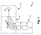
図1を参照すると、ビームブローアップを阻止するため、あるいは避けるために、イオン注入システムにおいて、光電子放射を介して空間電荷中和のために付加的に電子を供給する。図1において、簡略化して示した低エネルギーイオン注入システム10は、本発明にしたがって、概略、図示されており、ターミナル12、ビームラインアッセンブリ14およびエンドステーション16を含む。ターミナル12は、高電圧電源装置22によって電力が供給されるイオン源20を含み、イオンビーム24(図1Aに点線で示される)を形成し、ビームラインアッセンブリ14へ方向付ける。ビームラインアッセンブリ14は、ビームガイド32と、エンドステーション16内でウエハ30内へ適切な電荷対質量比のイオンのみを通過するようにダイポール磁場が定められる質量分析器26とを含む。
Referring to FIG. 1, additional electrons are provided for space charge neutralization via photoelectron emission in an ion implantation system to prevent or avoid beam blow-up. A simplified low energy
エンドステーション16は、シングルウエハワークピース30あるいは、ビームラインアッセンブリ14から整えられたビーム24を使用する、複数のウエハ30を並列イオン注入するため支持するのに適したバッチエンドステーションのような、どのタイプのエンドステーションでもよい。空間電荷中和を容易にし、それ故、ブローアップを阻止するために、イオン注入システム10は、さらに、光電子36の放射のため、光電子源へ光子を供給する光子源34を含むイオンビーム閉じ込め装置を含む。図のシステム10において、光電子源はビームガイド32の内壁であり、そして、光子源は、UVランプ、他のランプ、あるいはレーザであり、ビーム軌道に沿って空間電荷中和のための電子を追い出すために、ビームガイド壁へ十分なエネルギーの光子を供給する。任意の光子源も本発明の範囲内で使用できるが、例えば、レーザは、比較的狭い波長の範囲の単色光子を供給するために使用することができる。
The
図2は、本発明に従うビーム閉じ込め装置を有する、他の例示的イオン注入システム100を、略図で説明するものである。イオン注入機100は、イオン源112、ビームラインアッセンブリ115、およびエンドステーション116を含み、ビームガイド200は、ビームラインアッセンブリ115の少なくとも一部を介して延びる、イオンビーム128の輸送通路202を備えている。例示的なビームラインアッセンブリ115は、通路202の少なくとも一部に沿って光子源として機能するように、ランプ電源216に接続された複数のUVランプ220を含む。比較的狭い範囲の光子波長を有するUVランプは、光子源のエネルギー効率を最大限に利用するように選択され、また、レーザは、狭い波長範囲(例 単色)を供給するために使用される。
FIG. 2 schematically illustrates another exemplary
光電子源は、通路202に沿って設けられ、通路202は、1以上のビームガイド200の壁またはその一部、及び/またはビームガイド200の端部とエンドステーション116との間のビーム軌道に沿って位置する光電子源構造体221からなる。代わりにあるいは組み合わせて、分離された光電子源構造体221が、ビームガイド200内に設けられてよい。任意の光電子源が、本発明の範囲内の光電子源として使用されてよく、それは、以下、図8、9及び11により詳細に図解され、説明されているように、ビームガイドの全てあるいは一部、および/あるいはビームガイドから離れた構造である。
A photoelectron source is provided along the
ランプ220は、光電子源200および221の少なくとも一部へ光子を供給する光子源として作用し、ビーム128の空間電荷を中和するために光電子放射を引き起こす。ランプ220は、本発明の範囲内で、任意の形状、配置、および位置づけでもよく、図3−7に関していくつかの例が図に示され、記載されている。光電子源200および221の材料ばかりでなく、光子源220によって放射された光子のエネルギー、ランプ220から放射される光子の拡がるエネルギー、および放射された光子の波長範囲は、少なくとも光子の一部の光子エネルギーが、光電子源材料の仕事関数を越えるように選択される。それによって、図4Dに関して以下、記載されるように、ビームガイド壁200および/あるいは上記源構造体221の表面から光電子放射を与える。
The
光電子放射を増加するため、および源220から放射される電子をさらに閉じ込めるため、通路の少なくとも一部に複数のカスプ磁界を提供するように、以下、図10及び11に関して、図示され、より詳細に記載されるごとく、磁気装置240が、ビームラインアッセンブリ115内に設置される。さらに、光電子源220および/あるいは221は、光電子放射を増大し、および/あるいは、イオンビーム128の方へ発生した光電子の引き付けを容易にするため、バイアス電源217を使用してバイアスされる。そして、接地シールド219が、以下、図9および11に関して図示され、さらに説明されるように、ビーム128へのそのようなバイアスする電源の効果を制限するために使用される。
In order to increase the photoelectron emission and to further confine the electrons emitted from the
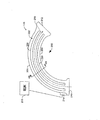
図3および4A−4Dを参照すると、より詳細な説明が、例示的なイオン注入システム100およびそのビーム閉じ込め装置についてなされている。図3に示すように、ビームラインアッセンブリ115は、エンドステーション116へ所定の電荷対質量比のイオンのみを選択的に提供するため、質量分析磁石114を含む。そして、ビームラインアッセンブリ115およびエンドステーション116は、ビームラインアッセンブリ115に関して、エンドステーション116の移動を可能にするために、伸張性ステンレススチール・ベローアッセンブリ118により結合される。イオン源112は、プラズマ室120および複数の電極を有するイオン・エキストラクタ・アッセンブリ122を含む。エネルギーは、プラズマ室120内にイオンを発生するために、イオン化ドーパントガスに与えられる。イオンは、イオン・エキストラクタ・アッセンブリ122によって、上記室120内のスリットを介してプラズマ室120から引き出され、プラズマ室120からの正イオンからなるイオンビーム128を作り出し、質量分析磁石114へ引き出されたイオンを加速する。
With reference to FIGS. 3 and 4A-4D, a more detailed description is provided for an exemplary
質量分析磁石114は、ビームラインアッセンブリ115内で、レゾルバハウジング123およびビーム中和器124を介して、エンドステーション116へ適切な電荷対質量比のイオンのみを提供する。ビーム128は、内側壁204および外側壁206を有するビームガイド200によって決められる通路202内の曲線状ビーム軌道208に沿って、質量分析磁石114内を伝播する。上記通路202は、真空ポンプ131によって排気される。通路208に沿って伝播するイオンビーム128は、質量分析磁石114によって発生したダイポール磁場の作用により、不適切な電荷対質量比のイオンをはねる。このダイポール磁場の強さと方向は、磁気コネクタ13を介する磁石114のフイールド・ワインディングにより、電流を調整する制御エレクトロニクス132によって制御される。
The
ダイポール磁場は、イオン源112近くのビームガイド入口端210の第1あるいは入射軌道134から、レゾルバハウジング123近くの出口端212の第2あるいは出口軌道135へ、曲線状ビーム軌道に沿って移動するイオンビーム128を生じる。不適切な電荷対質量比を有するイオンからなるビーム128の部分128´および128´´は、経路208の曲線状軌道から離れて、側壁204および206へ偏向され、あるいは、それぞれ、ビームガイド206のレゾルビングスリット123と衝突する。このように、質量分析器114は、所定の電荷対質量比を有するビーム128内のイオンのみを、レゾルバハウジング123を介して通過させる。
The dipole magnetic field travels along a curved beam trajectory from a first or
ビーム128は、このように質量分析され、ビームガイド200を介して、イオン源112から、ターミナル電極137、イオンビーム128を収束する静電レンズ138、およびファラディフラグ142のような線量測定指示器を含むレゾルバハウジング123へ輸送される。ビーム中和器124は、イオンビーム128を正に荷電させることで注入させる結果として、目標ウエハ上に蓄積する正電荷を中和するためのプラズマシャワー145を含む。ビーム中和器124およびレゾルバハウジング123は、真空ポンプ143によって排気される。
The
ビーム128は、エンドステーション116へ供給され、エンドステーション116は、その上にウエハWがビーム128による注入のために取り付けられている、円盤状ウエハ支持体144を含む。ウエハ支持体144は、注入ビーム128の方向に略垂直に向けられている目標平面内にあり、円盤状ウエハ支持体144は、エンドステーション116内のモータ146によって回転される。このように、イオンビーム128は、支持体に取り付けられ、円軌道を移動するウエハに衝突する。エンドステーション116は、イオンビームの軌道164およびウエハを横断する点162の周囲を旋回し、その結果、目標平面は、この点の周囲に調整可能である。
The
図4Aおよび4Bにさらに説明されるように、ビームガイド200は、イオンビーム軌道208に沿って、内外のアーチ状側壁204および206、上壁222および底壁225それぞれによって定められるアーチ形長手状通路202を備える。ビームガイド200は、入口端210から出口端212へ、この特別の実施形態では約135度の弧の角度で、
軌道208に沿って長さ方向に延びる。本発明は、いかなる角度の質量分析器と連結しても使用でき、そして、角度は、質量分解能およびビーム収束特性を満足させるように選ばれる。壁204,206、222、および224は、アルミニュウムから作られるけれども、代わりに他の光電子放出材料が本発明にしたがって使用されてよい。
As further illustrated in FIGS. 4A and 4B, the
It extends along the
ビームガイド200あるいはその部分が、光電子源として使用される実施形態で、ビームガイド200は、例えば、ランタンヘキサボライド(LaB6)のような仕事関数低下材料で被覆されるか、処理される。この点において、アルミニュウムは、約4.08eVの仕事関数であり、ランタンヘキサボライドは、約2.66eVの、より低い仕事関数を有する。ビームラインアッセンブリ115内の他の場所の他の光電子源構造体221および/又はビームガイド200内に設置される専用支持構造221(以下、図8,9、および11の構造221)は、同様に、低い仕事関数の光電子源を備えるように、そのような材料から作られるか、あるいは被覆される。以下の表は、本発明に従って単独で、あるいは組み合わせで光電子源構造を作るか、又は被覆して使用される材料の例を示している。
In embodiments where the

ビームガイド200あるいは他の光電子源221を作るおよび/または被覆するための材料は、低い仕事関数を提供するように選択され、それによって、光子源220、波長およびその出力仕様の選択に際して柔軟性を可能にする。材料選択は、コスト、製造の容易さ、耐久力、およびエンドステーション内でイオン注入されるウエハWの汚染可能性を含むがこれに限定されず、イオン注入に関する諸条件が考慮される。
The material for making and / or coating the
図3および4A−4Dは、本発明の可能な一実施形態を説明しており、複数のランプ220は、ビームガイド200のアーチ長さに沿って、上部および下部ビームガイド壁222および224それぞれに隣接して設置されている。ランプ電源216は、結合端子214を経由してランプ220に電力を供給しており、ランプ220への端子214からの配線(図示せず)は、ビームラインアッセンブリ215に沿って、ランプ220へ電源を供給する適切な方法で備えることが可能である。この例で、ランプ220は、ビーム軌道208の両側へ横方向に延び、光電子発生のためにビームガイド内壁表面(例 ビームガイド壁204、206、222および/あるいは224)へ光子を供給する紫外線(UV)を発生する。
3 and 4A-4D illustrate one possible embodiment of the present invention, where a plurality of
波長、出力定格、大きさ、方向、および/あるいはランプの配置は、空間電荷中和のために光電子源200,221から光電子放射を生じるように、少なくとも十分なエネルギーのいくらかの光子を供給するように選択される。さらに、光子源220は、レーザ220からの単色光、又はUVランプ220からの比較的小さい波長範囲のUV光のような、制御された波長の範囲の光子を供給するように配置されてもよい。イオンビームを中和するために必要とされる光電子の発生割合は、ビーム電流、システムの配列、およびビームガイド内の電子を閉じ込めるために選択される方法に依存する。
The wavelength, power rating, size, direction, and / or lamp placement will provide at least some photons of sufficient energy to produce photoemission from the
図4Dに示すように、例示的なUVランプ220は、ビームガイド200の壁から光電子230の放射を引き起こすように、少なくとも十分なエネルギーのいくらかの光子λを発生するのに適している。一実施形態において、ランプ220は、ビームガイド壁222および224から距離220Aだけ離れており、約3.125eV から約125eVの範囲のエネルギーを有する光子に相当する約1E−8mから約4E−7mの範囲の波長で、UV光を供給する。ビームガイド200および/あるいは光電子源構造体221は、アルミニュウム(例 仕事関数が約4.08eV)あるいは、ランタンヘキサボライド(例 仕事関数が約2.66eV)が被覆されたアルミニュウムから作られ、光電子源200,221に衝突する光子λの全てあるいはいくらか(例 ビームガイド壁224の底部の表面224a)は、ビーム128の空間電荷を中和するために光電子230を発生する。
As shown in FIG. 4D, the
今、図5A,5B、6および7を参照すると、ランプ220のかなり多数が、本発明(1以上)にしたがって備えられ、ランプ220は、適切な大きさおよび形状にすることができる。他の可能な実施形態は、図5Aおよび図5Bに説明されており、アーチ状ランプ220は、一般的に、ビームガイド200内のビーム軌道208と平行に延びている。図6に示すように、1以上の概して直状UVランプ220は、ビーム軌道208に沿って、概して長さ方向に延びるように配置することができる。他の可能な例は、図7に示されており、円形のランプ220が、本発明に従う光子の発生のために、ビームガイド200の内部に沿って、多くの箇所に設置される。
Referring now to FIGS. 5A, 5B, 6 and 7, a substantial number of
代わりにランプあるいはレーザ220は、図12に示すように、透明な窓225を通してビームガイド200の内部に沿って、光電子源200,221を照射するために、ビームガイド200の外側に配置される。UVランプ220を使用する一例において、窓225は、石英、カルシウムフルオライト(CaF2)あるいはマグネシウムフルオライト(MgF2)を含むがこれに限定されない、UV光に透明である材料から作られる。説明された例は、本発明の範囲内の可能な実施形態を網羅するものではなく、波長、波長範囲、出力定格、大きさ、配置、および/あるいはランプ220の配置は、光電子源200,221から光電子放射を引き起こすために、十分なエネルギーの光子を供給するように選択される。この点で、本発明はUVランプに制限されず、UVランプおよびレーザを含むがこれに限定されない、どの光子源20を使用しても実施できる。
Instead, a lamp or
図8を参照すると、光電子源構造体221は、ビームアッセンブリ115内に備えられ、任意の適切な光電子放出材料から、または光電子放出材料を被覆したものから作ることが可能である。光電子源構造体221は、ビームガイド内のような、イオン注入イオン源112とエンドステーション116間のどこにでも配置され(図3)、そして、光電子源構造体は、ビームガイドの壁から離れている。図8の例で、光電子源構造体221は、上部および底部のビームガイド壁222および224それぞれから、内側に離れている。光電子源構造体221が、任意の壁あるいはビームガイド200の壁(例 側壁204および/あるいは206)に沿って、あるいはビームラインアッセンブリ115(例 図3のレゾルバハウジング123内)内の任意の位置に据えられる、他の配置が可能であり、全てのそのような配置は、本発明および添付の請求の範囲の、範囲内のものであることを意図している。
Referring to FIG. 8, the
図9および11を参照すると、本発明の他の特徴は、ビームラインアッセンブリ115内で上記光電子源221から離れて導電シース219を備えており、上記光電子源221は、バイアス電源217を使用する導電シース219に関し、負にバイアスされる。本発明のこの特徴は、図10および11に示され、以下、さらに記述されるように、増加させる光電子放射のための磁場の設備と分離し、あるいは組み合わせて使用され、および/あるいは軌道208に沿うビームに供給される中和する光電子の量を改善するために使用される。
Referring to FIGS. 9 and 11, another feature of the present invention includes a
正イオンビーム128は、ウエハW(例 図2および3)をイオン注入するために使用され、イオンビーム電位は、概して、接地されたビームガイド側壁に関して正である。側壁とイオンビーム自体との間の電位は、ビームガイド表面から発生した光電子を離すのに不十分である。図9および11のバイアシングは、軌道208に沿う光電子源221とビーム128間の電位の調整を可能にし、バイアス電源217は、一例において、ゼロから約200ボルトの範囲で、負のDCバイアスを供給するように制御エレクトロニクス132(図3)によって制御することができる。
A
ビーム128の方へ光電子を向けることに加えて、上記バイアシングは、また、光電子源構造体221からの光電子放射を増加させる。図9および11の例において、光電子源構造体221は、ビームガイド200の壁から内側に離れており、細長い穴が開いた接地シールド又はシース219は、上記源221から内側に離れており、そのため、バイアス源構造体221からの電場は、ビーム128自体と干渉しない。一方、電場は、光電子放出材料の仕事関数を大きく低めるようにしないが、接地に対して上記光電子源構造体221をバイアスすることから生じる電場は、イオンビーム128へ光電子をより容易に向けるように作用する。
In addition to directing photoelectrons toward the
上記ビームは、ますます中和されるので、正のビーム電位は、ますます低くなり、そして、光電子源構造体のバイアシングは、ビーム中へ放射される電子を押し出すように、光電子放出表面で付加的な電位を有利に供給する。この点について、数ボルトほどのバイアスは、ビームガイド壁への改善された性能を提供し、任意のバイアス電位が本発明の範囲内で可能であるけれども、それらは負の電位になり、押し返される。さらに、この配置で作られるバイアス電位は、ビームガイド200の体積内で電子を閉じ込める働きをする(例 電子がビーム128の方へ近づく動きをする時)。 As the beam is increasingly neutralized, the positive beam potential becomes increasingly lower, and the biasing of the photoelectron source structure is added at the photoemission surface to push out the emitted electrons into the beam. An advantageous potential. In this regard, biases on the order of a few volts provide improved performance to the beam guide wall, and although any bias potential is possible within the scope of the present invention, they will be negative and push back. It is. Furthermore, the bias potential created in this arrangement serves to confine electrons within the volume of the beam guide 200 (eg, when the electrons move toward the beam 128).
このように、上記バイアシング並びに上記源材料および/あるいは被覆の選択は、空間電荷中和のために十分な光電子放射を提供するために使用され、また、より低い出力での光子源220の使用を可能にする。そして、上記バイアシングおよび上記源材料は、UVランプまたは他のような、商業的に利用可能な光子源220の使用を容易にするよう選択される。図9および11に示されるように、接地されたシース219は、ビーム128の方へ電場を向け、その結果、発生した光電子は、正のイオンビームの方へより容易に移動しようとする。シース219は、また、光電子源221の電場からビーム128を遮蔽するように作用する。さらに、シース219は、ビーム128からの直接の衝突から光電子放出表面を保護するように、部分的遮蔽として働く。シース219は、ビーム128へ進むべく放射された光電子のための径路を提供するために、スロット219aのような1以上の開口を含む。
Thus, the biasing and selection of the source material and / or coating can be used to provide sufficient photoelectron emission for space charge neutralization, and the use of the
図10および11を参照すると、本発明の他の特徴は、ビームラインアッセンブリ115内に磁気装置240を備えており、通路202の少なくとも一部分で複数のカスプ磁界232を発生する。磁気装置240は、好ましくは、生じる磁場232がビームガイド壁からイオンビームへ、光電子の供給を妨げないように配置される。上記磁場232は、任意の適切な磁気装置240を使用して与えることが可能であり、上記磁場232は、ビームラインアッセンブリ115内の電子の閉じ込めを増大するように作用する。図10と11の例において、複数の永久磁石240は、少なくとも通路202の部分に沿って配置され、磁石240は、上部および下部ビームガイド壁222および224それぞれの外側表面にある。他の実施形態では、磁石240が通路202の一部分で複数のカスプ磁界を与えるように、ビームラインアッセンブリ115に沿うどこかに配置できる。
Referring to FIGS. 10 and 11, another feature of the present invention includes a
可能な一実施形態では、磁気装置240は、代わりに、ビームガイド200の側壁204と206に沿って備えられて、フォトンが、ビームの空間電荷中和のための光電子放射のため、上部および下部ビームガイド壁222および224へ向けられる。図10および11に見られるように、磁気装置240は、単独で、あるいは上述のようにバイアシング技術と組み合わせて、光電子放射増大のために使用される。そのような全ての実施形態が、本発明および添付の請求の範囲の、範囲内であることが意図されている。
In one possible embodiment, the
本発明は1以上の実施形態について描かれ、記述されているけれども、代替および変更が、添付の請求の範囲の精神および範囲を逸脱すること無しに、説明例が作られることは可能である。特に、上述した要素あるいは構造(ブロック、ユニット、エンジン、アッセンブリ、装置、回路、システム等)によって達成される種々の機能について、そのような要素を記述するために使用される用語(“手段”への言及を含む)は、他に示されなければ、
たとえ本発明のここに説明された例示的実施形態に構造的に等しくなくても、上述の要素(例 機能的に等しい)の特定の機能を達成する要素あるいは構造に相応することを意味する。
While the invention has been illustrated and described with respect to one or more embodiments, alternatives and modifications may be made without departing from the spirit and scope of the appended claims. In particular, for the various functions achieved by the elements or structures described above (blocks, units, engines, assemblies, devices, circuits, systems, etc.), the terms used to describe such elements (to "means") Unless otherwise indicated)
It is meant to correspond to an element or structure that achieves a particular function of the above-described elements (eg, functionally equivalent), even though they are not structurally equivalent to the exemplary embodiments described herein of the present invention.
さらに本発明の特定の特徴が、いくつかの実施形態のうちの一つについて開示されているけれども、そのような特徴は、与えられたあるいは特定の適用のために、所定の、そして有利である他の実施形態の内の、一つ以上の他の特徴と組み合わせることが可能である。さらにまた、詳細な説明および請求の範囲のどちらかで使用されている「含むこと」、「含む」、「有すること」、「有する」、「備え」あるいはそれらの変形の範囲内において、そのような用語は、ある意味で「包含する」という用語の類似に含まれるものであることを意味する。 Furthermore, although specific features of the invention are disclosed for one of several embodiments, such features are predetermined and advantageous for a given or specific application. It can be combined with one or more other features in other embodiments. Furthermore, within the scope of “including”, “including”, “having”, “having”, “comprising” or variations thereof as used in either the detailed description and the claims. Is meant to be included in a sense similar to the term “including”.
Claims (49)
前記径路に沿ってイオン源から下流に設置されるビームラインアッセンブリとを含むイオン注入システムであって、前記ビームラインアッセンブリは、
前記イオンビームが前記径路に沿って運搬される通路を定めるビームガイドと、
少なくとも前記通路の一部分に沿って設けられる光電子源と、
前記光電子源から光電子放射を引き起こすように、少なくとも前記光電子源の一部分に光子を供給する光子源と、
前記径路に沿って、前記ビームラインアッセンブリの下流に設けられ、イオンビームを使用するイオン注入のための前記径路にそって、少なくとも一つのウエハを支持するように適合しているエンドステーションと、
からなることを特徴とするイオン注入システム。 An ion source suitable for producing an ion beam along a path;
A beam line assembly installed downstream from the ion source along the path, the beam line assembly comprising:
A beam guide that defines a path through which the ion beam is conveyed along the path;
A photoelectron source provided along at least a portion of the passage;
A photon source for supplying photons to at least a portion of the photoelectron source so as to cause photoelectron emission from the photoelectron source;
An end station provided downstream of the beam line assembly along the path and adapted to support at least one wafer along the path for ion implantation using an ion beam;
An ion implantation system comprising:
少なくとも通路の部分に沿って配置される光電子源と、
光電子源から光電子放射を引き起こすように、少なくとも光電子源の一部分へ光子を供給する光子源とを、含むことを特徴とするビーム閉じ込め装置。 A beam confinement device for preventing ion beam blow-up in an ion beam transport path, the confinement device comprising:
A photoelectron source disposed along at least a portion of the passageway;
A beam confinement device comprising: a photon source for supplying photons to at least a portion of the photoelectron source so as to cause photoelectron emission from the photoelectron source.
イオンビーム径路に沿って光電子源を備え、
そして、光電子源から光電子放射を引き起こすように、少なくとも光電子源の一部分に光子を供給することを特徴とする方法。 A method for providing ion beam confinement in an ion implantation system, the method comprising:
A photoelectron source is provided along the ion beam path,
And supplying photons to at least a portion of the photoelectron source so as to cause photoelectron emission from the photoelectron source.
このビームガイドは、前記径路に沿ってイオンビームが輸送される通路を定め、
そして、光子を供給することは、前記ビームガイドから光電子放射を引き起こすように、ビームガイドの少なくとも一部分に光子を供給することを含むことを特徴とする請求項43の方法。 The photoelectron source comprises a beam guide downstream from the ion source;
The beam guide defines a path along which the ion beam is transported along the path,
44. The method of claim 43, wherein providing a photon includes providing a photon to at least a portion of the beam guide to cause photoelectron emission from the beam guide.
光電子を増加するために、前記導電シースに関して前記光電子源を負にバイアスすること特徴とする請求項43の方法。 A conductive sheath remote from the photoelectron source;
44. The method of claim 43, wherein the source of photoelectrons is negatively biased with respect to the conductive sheath to increase photoelectrons.
Applications Claiming Priority (2)
| Application Number | Priority Date | Filing Date | Title |
|---|---|---|---|
| US10/632,234 US6891174B2 (en) | 2003-07-31 | 2003-07-31 | Method and system for ion beam containment using photoelectrons in an ion beam guide |
| PCT/US2004/025310 WO2005013341A2 (en) | 2003-07-31 | 2004-07-30 | Method and system for ion beam containment using photoelectrons in an ion beam guide |
Publications (1)
| Publication Number | Publication Date |
|---|---|
| JP2007500924A true JP2007500924A (en) | 2007-01-18 |
Family
ID=34104311
Family Applications (1)
| Application Number | Title | Priority Date | Filing Date |
|---|---|---|---|
| JP2006522146A Pending JP2007500924A (en) | 2003-07-31 | 2004-07-30 | Apparatus and method for confining an ion beam using photoelectrons in an ion beam guide |
Country Status (4)
| Country | Link |
|---|---|
| US (1) | US6891174B2 (en) |
| JP (1) | JP2007500924A (en) |
| TW (1) | TW200509262A (en) |
| WO (1) | WO2005013341A2 (en) |
Families Citing this family (9)
| Publication number | Priority date | Publication date | Assignee | Title |
|---|---|---|---|---|
| US7606791B2 (en) * | 2004-06-03 | 2009-10-20 | International Business Machines Corporation | Internal parameters (parameters aging) in an abstract query |
| US6989545B1 (en) * | 2004-07-07 | 2006-01-24 | Axcelis Technologies, Inc. | Device and method for measurement of beam angle and divergence |
| US7402816B2 (en) * | 2004-11-19 | 2008-07-22 | Varian Semiconductor Equipment Associates, Inc. | Electron injection in ion implanter magnets |
| US7439526B2 (en) * | 2004-12-20 | 2008-10-21 | Varian Semiconductor Equipment Associates, Inc. | Beam neutralization in low-energy high-current ribbon-beam implanters |
| DE102005056698B4 (en) * | 2005-11-28 | 2008-11-27 | Siemens Ag | Medical radiotherapy device with displaceable position of the beam exit window |
| JP4825028B2 (en) * | 2006-03-17 | 2011-11-30 | 浜松ホトニクス株式会社 | Ionizer |
| JP4958258B2 (en) | 2006-03-17 | 2012-06-20 | 株式会社リガク | Gas analyzer |
| US7655922B2 (en) * | 2006-12-07 | 2010-02-02 | Varian Semiconductor Equipment Associates, Inc. | Techniques for confining electrons in an ion implanter |
| US7800083B2 (en) * | 2007-11-06 | 2010-09-21 | Axcelis Technologies, Inc. | Plasma electron flood for ion beam implanter |
Citations (8)
| Publication number | Priority date | Publication date | Assignee | Title |
|---|---|---|---|---|
| JPS63126147A (en) * | 1986-11-14 | 1988-05-30 | Fujitsu Ltd | Electric charge neutralizing unit for ion radiation device |
| JPH0275139A (en) * | 1988-09-09 | 1990-03-14 | Oki Electric Ind Co Ltd | Ion implanting device |
| JPH05290789A (en) * | 1992-04-07 | 1993-11-05 | Mitsubishi Electric Corp | Ion implantation device |
| JPH0689690A (en) * | 1992-09-07 | 1994-03-29 | Nec Yamagata Ltd | Ion beam neutralizing device for ion implanting device |
| JPH08190883A (en) * | 1995-01-13 | 1996-07-23 | Sumitomo Electric Ind Ltd | Electron beam exposing device |
| JP2002515634A (en) * | 1998-05-12 | 2002-05-28 | アプライド マテリアルズ インコーポレイテッド | Ion beam apparatus and method for neutralizing space charge of ion beam |
| JP2003197144A (en) * | 2001-12-27 | 2003-07-11 | Sumitomo Eaton Noba Kk | Ion beam processing method and processing device |
| JP2003215916A (en) * | 2002-01-25 | 2003-07-30 | Sharp Corp | Electrifying device |
Family Cites Families (41)
| Publication number | Priority date | Publication date | Assignee | Title |
|---|---|---|---|---|
| US4383177A (en) * | 1980-12-24 | 1983-05-10 | International Business Machines Corporation | Multipole implantation-isotope separation ion beam source |
| US4447732A (en) * | 1982-05-04 | 1984-05-08 | The United States Of America As Represented By The United States Department Of Energy | Ion source |
| US4686365A (en) * | 1984-12-24 | 1987-08-11 | American Cyanamid Company | Fourier transform ion cyclothon resonance mass spectrometer with spatially separated sources and detector |
| US4714860A (en) * | 1985-01-30 | 1987-12-22 | Brown Ian G | Ion beam generating apparatus |
| FR2595868B1 (en) * | 1986-03-13 | 1988-05-13 | Commissariat Energie Atomique | ION SOURCE WITH ELECTRONIC CYCLOTRON RESONANCE WITH COAXIAL INJECTION OF ELECTROMAGNETIC WAVES |
| US5433788A (en) * | 1987-01-19 | 1995-07-18 | Hitachi, Ltd. | Apparatus for plasma treatment using electron cyclotron resonance |
| JPS63291337A (en) * | 1987-05-22 | 1988-11-29 | Sharp Corp | Photo-cathode |
| US5206516A (en) * | 1991-04-29 | 1993-04-27 | International Business Machines Corporation | Low energy, steered ion beam deposition system having high current at low pressure |
| JPH05205691A (en) * | 1992-01-27 | 1993-08-13 | Nec Yamagata Ltd | Ion implantation device |
| US5466929A (en) * | 1992-02-21 | 1995-11-14 | Hitachi, Ltd. | Apparatus and method for suppressing electrification of sample in charged beam irradiation apparatus |
| JPH0636735A (en) | 1992-07-16 | 1994-02-10 | Japan Steel Works Ltd:The | Substrate manufacturing device by polyvalent ion implanting method and manufacture of substrate |
| US5350926A (en) * | 1993-03-11 | 1994-09-27 | Diamond Semiconductor Group, Inc. | Compact high current broad beam ion implanter |
| US5523652A (en) * | 1994-09-26 | 1996-06-04 | Eaton Corporation | Microwave energized ion source for ion implantation |
| US5497006A (en) * | 1994-11-15 | 1996-03-05 | Eaton Corporation | Ion generating source for use in an ion implanter |
| JP3123735B2 (en) * | 1995-04-28 | 2001-01-15 | 株式会社日立製作所 | Ion beam processing equipment |
| US5554857A (en) * | 1995-10-19 | 1996-09-10 | Eaton Corporation | Method and apparatus for ion beam formation in an ion implanter |
| US5811823A (en) * | 1996-02-16 | 1998-09-22 | Eaton Corporation | Control mechanisms for dosimetry control in ion implantation systems |
| US5825038A (en) * | 1996-11-26 | 1998-10-20 | Eaton Corporation | Large area uniform ion beam formation |
| US5760405A (en) * | 1996-02-16 | 1998-06-02 | Eaton Corporation | Plasma chamber for controlling ion dosage in ion implantation |
| US5661308A (en) * | 1996-05-30 | 1997-08-26 | Eaton Corporation | Method and apparatus for ion formation in an ion implanter |
| JP3284886B2 (en) * | 1996-06-20 | 2002-05-20 | 株式会社日立製作所 | Ion source and ion implanter |
| US5707452A (en) * | 1996-07-08 | 1998-01-13 | Applied Microwave Plasma Concepts, Inc. | Coaxial microwave applicator for an electron cyclotron resonance plasma source |
| US5975014A (en) * | 1996-07-08 | 1999-11-02 | Asm Japan K.K. | Coaxial resonant multi-port microwave applicator for an ECR plasma source |
| US5834786A (en) * | 1996-07-15 | 1998-11-10 | Diamond Semiconductor Group, Inc. | High current ribbon beam ion implanter |
| US5703375A (en) * | 1996-08-02 | 1997-12-30 | Eaton Corporation | Method and apparatus for ion beam neutralization |
| US5703372A (en) * | 1996-10-30 | 1997-12-30 | Eaton Corporation | Endcap for indirectly heated cathode of ion source |
| GB9710380D0 (en) * | 1997-05-20 | 1997-07-16 | Applied Materials Inc | Electron flood apparatus for neutralising charge build-up on a substrate during ion implantation |
| JP3627206B2 (en) * | 1997-11-28 | 2005-03-09 | 住友イートンノバ株式会社 | Ion implantation apparatus and ion implantation method |
| US6271529B1 (en) * | 1997-12-01 | 2001-08-07 | Ebara Corporation | Ion implantation with charge neutralization |
| US6016036A (en) * | 1998-01-28 | 2000-01-18 | Eaton Corporation | Magnetic filter for ion source |
| US6060718A (en) * | 1998-02-26 | 2000-05-09 | Eaton Corporation | Ion source having wide output current operating range |
| US6135128A (en) * | 1998-03-27 | 2000-10-24 | Eaton Corporation | Method for in-process cleaning of an ion source |
| US6294862B1 (en) * | 1998-05-19 | 2001-09-25 | Eaton Corporation | Multi-cusp ion source |
| US6130436A (en) * | 1998-06-02 | 2000-10-10 | Varian Semiconductor Equipment Associates, Inc. | Acceleration and analysis architecture for ion implanter |
| US6359286B1 (en) * | 1998-07-10 | 2002-03-19 | Applied Materials, Inc. | Method and apparatus for neutralizing space charge in an ion beam |
| US6207963B1 (en) * | 1998-12-23 | 2001-03-27 | Axcelis Technologies, Inc. | Ion beam implantation using conical magnetic scanning |
| US6313457B1 (en) * | 1999-01-25 | 2001-11-06 | Gentex Corporation | Moisture detecting system using semiconductor light sensor with integral charge collection |
| JP3608416B2 (en) * | 1999-02-02 | 2005-01-12 | 日新電機株式会社 | Plasma source |
| US6207964B1 (en) * | 1999-02-19 | 2001-03-27 | Axcelis Technologies, Inc. | Continuously variable aperture for high-energy ion implanter |
| US6541781B1 (en) * | 2000-07-25 | 2003-04-01 | Axcelis Technologies, Inc. | Waveguide for microwave excitation of plasma in an ion beam guide |
| US6414329B1 (en) * | 2000-07-25 | 2002-07-02 | Axcelis Technologies, Inc. | Method and system for microwave excitation of plasma in an ion beam guide |
-
2003
- 2003-07-31 US US10/632,234 patent/US6891174B2/en not_active Expired - Fee Related
-
2004
- 2004-07-30 TW TW093122874A patent/TW200509262A/en unknown
- 2004-07-30 WO PCT/US2004/025310 patent/WO2005013341A2/en active Application Filing
- 2004-07-30 JP JP2006522146A patent/JP2007500924A/en active Pending
Patent Citations (8)
| Publication number | Priority date | Publication date | Assignee | Title |
|---|---|---|---|---|
| JPS63126147A (en) * | 1986-11-14 | 1988-05-30 | Fujitsu Ltd | Electric charge neutralizing unit for ion radiation device |
| JPH0275139A (en) * | 1988-09-09 | 1990-03-14 | Oki Electric Ind Co Ltd | Ion implanting device |
| JPH05290789A (en) * | 1992-04-07 | 1993-11-05 | Mitsubishi Electric Corp | Ion implantation device |
| JPH0689690A (en) * | 1992-09-07 | 1994-03-29 | Nec Yamagata Ltd | Ion beam neutralizing device for ion implanting device |
| JPH08190883A (en) * | 1995-01-13 | 1996-07-23 | Sumitomo Electric Ind Ltd | Electron beam exposing device |
| JP2002515634A (en) * | 1998-05-12 | 2002-05-28 | アプライド マテリアルズ インコーポレイテッド | Ion beam apparatus and method for neutralizing space charge of ion beam |
| JP2003197144A (en) * | 2001-12-27 | 2003-07-11 | Sumitomo Eaton Noba Kk | Ion beam processing method and processing device |
| JP2003215916A (en) * | 2002-01-25 | 2003-07-30 | Sharp Corp | Electrifying device |
Also Published As
| Publication number | Publication date |
|---|---|
| US20050023487A1 (en) | 2005-02-03 |
| WO2005013341A2 (en) | 2005-02-10 |
| US6891174B2 (en) | 2005-05-10 |
| TW200509262A (en) | 2005-03-01 |
| WO2005013341A3 (en) | 2005-08-25 |
Similar Documents
| Publication | Publication Date | Title |
|---|---|---|
| JP5120598B2 (en) | Acceleration / deceleration gap for deflection | |
| JP4793696B2 (en) | Method and apparatus for selective pre-dispersion of an extracted ion beam in an ion implantation system | |
| KR101653725B1 (en) | Post-decel magnetic energy filter for ion implantation systems | |
| US7800083B2 (en) | Plasma electron flood for ion beam implanter | |
| KR100855135B1 (en) | Electrostatic trap for particles entrained in an ion beam | |
| US9679739B2 (en) | Combined electrostatic lens system for ion implantation | |
| US6998625B1 (en) | Ion implanter having two-stage deceleration beamline | |
| JPH10312770A (en) | Electrostatic triode lens, ion implantation apparatus, and ion beam focusing method | |
| JP4831419B2 (en) | Magnetron structure for thin film formation for generating plasma in ion implantation system | |
| KR100855134B1 (en) | System and method for removing particles entrained in an ion beam | |
| KR100904313B1 (en) | System and method for removing contaminant particles relative to an ion beam | |
| US6891174B2 (en) | Method and system for ion beam containment using photoelectrons in an ion beam guide | |
| JP2007507077A (en) | Extraction method of ion beam slit with mass separation | |
| US20100019141A1 (en) | Energy contamination monitor with neutral current detection | |
| US20040227106A1 (en) | System and methods for ion beam containment using localized electrostatic fields in an ion beam passageway | |
| WO2006124075A2 (en) | System and methods for ion beam containment using localized electrostatic fields in an ion beam passageway |
Legal Events
| Date | Code | Title | Description |
|---|---|---|---|
| A621 | Written request for application examination |
Free format text: JAPANESE INTERMEDIATE CODE: A621 Effective date: 20070725 |
|
| A977 | Report on retrieval |
Free format text: JAPANESE INTERMEDIATE CODE: A971007 Effective date: 20100520 |
|
| A131 | Notification of reasons for refusal |
Free format text: JAPANESE INTERMEDIATE CODE: A131 Effective date: 20100602 |
|
| A02 | Decision of refusal |
Free format text: JAPANESE INTERMEDIATE CODE: A02 Effective date: 20101104 |