JP2007304594A - Image display system and method for driving display elements - Google Patents
Image display system and method for driving display elements Download PDFInfo
- Publication number
- JP2007304594A JP2007304594A JP2007123022A JP2007123022A JP2007304594A JP 2007304594 A JP2007304594 A JP 2007304594A JP 2007123022 A JP2007123022 A JP 2007123022A JP 2007123022 A JP2007123022 A JP 2007123022A JP 2007304594 A JP2007304594 A JP 2007304594A
- Authority
- JP
- Japan
- Prior art keywords
- storage capacitor
- terminal
- transistor
- node
- signal
- Prior art date
- Legal status (The legal status is an assumption and is not a legal conclusion. Google has not performed a legal analysis and makes no representation as to the accuracy of the status listed.)
- Pending
Links
Images


Classifications
-
- G—PHYSICS
- G09—EDUCATION; CRYPTOGRAPHY; DISPLAY; ADVERTISING; SEALS
- G09G—ARRANGEMENTS OR CIRCUITS FOR CONTROL OF INDICATING DEVICES USING STATIC MEANS TO PRESENT VARIABLE INFORMATION
- G09G3/00—Control arrangements or circuits, of interest only in connection with visual indicators other than cathode-ray tubes
- G09G3/20—Control arrangements or circuits, of interest only in connection with visual indicators other than cathode-ray tubes for presentation of an assembly of a number of characters, e.g. a page, by composing the assembly by combination of individual elements arranged in a matrix no fixed position being assigned to or needed to be assigned to the individual characters or partial characters
- G09G3/22—Control arrangements or circuits, of interest only in connection with visual indicators other than cathode-ray tubes for presentation of an assembly of a number of characters, e.g. a page, by composing the assembly by combination of individual elements arranged in a matrix no fixed position being assigned to or needed to be assigned to the individual characters or partial characters using controlled light sources
- G09G3/30—Control arrangements or circuits, of interest only in connection with visual indicators other than cathode-ray tubes for presentation of an assembly of a number of characters, e.g. a page, by composing the assembly by combination of individual elements arranged in a matrix no fixed position being assigned to or needed to be assigned to the individual characters or partial characters using controlled light sources using electroluminescent panels
- G09G3/32—Control arrangements or circuits, of interest only in connection with visual indicators other than cathode-ray tubes for presentation of an assembly of a number of characters, e.g. a page, by composing the assembly by combination of individual elements arranged in a matrix no fixed position being assigned to or needed to be assigned to the individual characters or partial characters using controlled light sources using electroluminescent panels semiconductive, e.g. using light-emitting diodes [LED]
- G09G3/3208—Control arrangements or circuits, of interest only in connection with visual indicators other than cathode-ray tubes for presentation of an assembly of a number of characters, e.g. a page, by composing the assembly by combination of individual elements arranged in a matrix no fixed position being assigned to or needed to be assigned to the individual characters or partial characters using controlled light sources using electroluminescent panels semiconductive, e.g. using light-emitting diodes [LED] organic, e.g. using organic light-emitting diodes [OLED]
- G09G3/3225—Control arrangements or circuits, of interest only in connection with visual indicators other than cathode-ray tubes for presentation of an assembly of a number of characters, e.g. a page, by composing the assembly by combination of individual elements arranged in a matrix no fixed position being assigned to or needed to be assigned to the individual characters or partial characters using controlled light sources using electroluminescent panels semiconductive, e.g. using light-emitting diodes [LED] organic, e.g. using organic light-emitting diodes [OLED] using an active matrix
- G09G3/3233—Control arrangements or circuits, of interest only in connection with visual indicators other than cathode-ray tubes for presentation of an assembly of a number of characters, e.g. a page, by composing the assembly by combination of individual elements arranged in a matrix no fixed position being assigned to or needed to be assigned to the individual characters or partial characters using controlled light sources using electroluminescent panels semiconductive, e.g. using light-emitting diodes [LED] organic, e.g. using organic light-emitting diodes [OLED] using an active matrix with pixel circuitry controlling the current through the light-emitting element
-
- G—PHYSICS
- G09—EDUCATION; CRYPTOGRAPHY; DISPLAY; ADVERTISING; SEALS
- G09G—ARRANGEMENTS OR CIRCUITS FOR CONTROL OF INDICATING DEVICES USING STATIC MEANS TO PRESENT VARIABLE INFORMATION
- G09G3/00—Control arrangements or circuits, of interest only in connection with visual indicators other than cathode-ray tubes
- G09G3/20—Control arrangements or circuits, of interest only in connection with visual indicators other than cathode-ray tubes for presentation of an assembly of a number of characters, e.g. a page, by composing the assembly by combination of individual elements arranged in a matrix no fixed position being assigned to or needed to be assigned to the individual characters or partial characters
- G09G3/22—Control arrangements or circuits, of interest only in connection with visual indicators other than cathode-ray tubes for presentation of an assembly of a number of characters, e.g. a page, by composing the assembly by combination of individual elements arranged in a matrix no fixed position being assigned to or needed to be assigned to the individual characters or partial characters using controlled light sources
- G09G3/30—Control arrangements or circuits, of interest only in connection with visual indicators other than cathode-ray tubes for presentation of an assembly of a number of characters, e.g. a page, by composing the assembly by combination of individual elements arranged in a matrix no fixed position being assigned to or needed to be assigned to the individual characters or partial characters using controlled light sources using electroluminescent panels
-
- G—PHYSICS
- G09—EDUCATION; CRYPTOGRAPHY; DISPLAY; ADVERTISING; SEALS
- G09G—ARRANGEMENTS OR CIRCUITS FOR CONTROL OF INDICATING DEVICES USING STATIC MEANS TO PRESENT VARIABLE INFORMATION
- G09G3/00—Control arrangements or circuits, of interest only in connection with visual indicators other than cathode-ray tubes
- G09G3/20—Control arrangements or circuits, of interest only in connection with visual indicators other than cathode-ray tubes for presentation of an assembly of a number of characters, e.g. a page, by composing the assembly by combination of individual elements arranged in a matrix no fixed position being assigned to or needed to be assigned to the individual characters or partial characters
- G09G3/22—Control arrangements or circuits, of interest only in connection with visual indicators other than cathode-ray tubes for presentation of an assembly of a number of characters, e.g. a page, by composing the assembly by combination of individual elements arranged in a matrix no fixed position being assigned to or needed to be assigned to the individual characters or partial characters using controlled light sources
- G09G3/30—Control arrangements or circuits, of interest only in connection with visual indicators other than cathode-ray tubes for presentation of an assembly of a number of characters, e.g. a page, by composing the assembly by combination of individual elements arranged in a matrix no fixed position being assigned to or needed to be assigned to the individual characters or partial characters using controlled light sources using electroluminescent panels
- G09G3/32—Control arrangements or circuits, of interest only in connection with visual indicators other than cathode-ray tubes for presentation of an assembly of a number of characters, e.g. a page, by composing the assembly by combination of individual elements arranged in a matrix no fixed position being assigned to or needed to be assigned to the individual characters or partial characters using controlled light sources using electroluminescent panels semiconductive, e.g. using light-emitting diodes [LED]
-
- H—ELECTRICITY
- H05—ELECTRIC TECHNIQUES NOT OTHERWISE PROVIDED FOR
- H05B—ELECTRIC HEATING; ELECTRIC LIGHT SOURCES NOT OTHERWISE PROVIDED FOR; CIRCUIT ARRANGEMENTS FOR ELECTRIC LIGHT SOURCES, IN GENERAL
- H05B33/00—Electroluminescent light sources
- H05B33/12—Light sources with substantially two-dimensional radiating surfaces
-
- G—PHYSICS
- G09—EDUCATION; CRYPTOGRAPHY; DISPLAY; ADVERTISING; SEALS
- G09G—ARRANGEMENTS OR CIRCUITS FOR CONTROL OF INDICATING DEVICES USING STATIC MEANS TO PRESENT VARIABLE INFORMATION
- G09G2300/00—Aspects of the constitution of display devices
- G09G2300/08—Active matrix structure, i.e. with use of active elements, inclusive of non-linear two terminal elements, in the pixels together with light emitting or modulating elements
- G09G2300/0809—Several active elements per pixel in active matrix panels
- G09G2300/0819—Several active elements per pixel in active matrix panels used for counteracting undesired variations, e.g. feedback or autozeroing
-
- G—PHYSICS
- G09—EDUCATION; CRYPTOGRAPHY; DISPLAY; ADVERTISING; SEALS
- G09G—ARRANGEMENTS OR CIRCUITS FOR CONTROL OF INDICATING DEVICES USING STATIC MEANS TO PRESENT VARIABLE INFORMATION
- G09G2300/00—Aspects of the constitution of display devices
- G09G2300/08—Active matrix structure, i.e. with use of active elements, inclusive of non-linear two terminal elements, in the pixels together with light emitting or modulating elements
- G09G2300/0809—Several active elements per pixel in active matrix panels
- G09G2300/0842—Several active elements per pixel in active matrix panels forming a memory circuit, e.g. a dynamic memory with one capacitor
- G09G2300/0861—Several active elements per pixel in active matrix panels forming a memory circuit, e.g. a dynamic memory with one capacitor with additional control of the display period without amending the charge stored in a pixel memory, e.g. by means of additional select electrodes
-
- G—PHYSICS
- G09—EDUCATION; CRYPTOGRAPHY; DISPLAY; ADVERTISING; SEALS
- G09G—ARRANGEMENTS OR CIRCUITS FOR CONTROL OF INDICATING DEVICES USING STATIC MEANS TO PRESENT VARIABLE INFORMATION
- G09G2320/00—Control of display operating conditions
- G09G2320/02—Improving the quality of display appearance
- G09G2320/0223—Compensation for problems related to R-C delay and attenuation in electrodes of matrix panels, e.g. in gate electrodes or on-substrate video signal electrodes
-
- G—PHYSICS
- G09—EDUCATION; CRYPTOGRAPHY; DISPLAY; ADVERTISING; SEALS
- G09G—ARRANGEMENTS OR CIRCUITS FOR CONTROL OF INDICATING DEVICES USING STATIC MEANS TO PRESENT VARIABLE INFORMATION
- G09G2320/00—Control of display operating conditions
- G09G2320/02—Improving the quality of display appearance
- G09G2320/0233—Improving the luminance or brightness uniformity across the screen
Landscapes
- Engineering & Computer Science (AREA)
- Physics & Mathematics (AREA)
- Computer Hardware Design (AREA)
- General Physics & Mathematics (AREA)
- Theoretical Computer Science (AREA)
- Control Of Indicators Other Than Cathode Ray Tubes (AREA)
- Control Of El Displays (AREA)
- Electroluminescent Light Sources (AREA)
Abstract
Description
本発明は、画素駆動回路に関し、特に、スレッショルド電圧と電力供給を補償する画素駆動回路に関するものである。 The present invention relates to a pixel driving circuit, and more particularly to a pixel driving circuit that compensates for a threshold voltage and power supply.
有機化合物を発光材料として用いて光を発する有機発光ダイオード(OLED)ディスプレイは、平面ディスプレイである。OLEDディスプレイの利点は、小型、軽量、広視野角、高コントラスト比と、高速であることである。 An organic light emitting diode (OLED) display that emits light using an organic compound as a light emitting material is a flat display. The advantages of OLED displays are small size, light weight, wide viewing angle, high contrast ratio, and high speed.
アクティブマトリクス有機発光ダイオード(AMOLED)ディスプレイは、目下、次世代のフラットパネルディスプレイとして頭角を現している。アクティブマトリクス液晶ディスプレイ(AMLCD)に比べ、AMOLEDディスプレイは、例えば、高コントラスト比、広視野角、バックライトのない薄型モジュール、低消費電力と、低コストなどの多くの利点を有する。電圧源によって駆動されるAMLCDと異なって、AMOLEDディスプレイは、電流源を必要として表示素子EL(lectroluminescent)を駆動する。表示素子ELの輝度は、伝導された電流に比例する。電流レベルの変動は、AMOLEDディスプレイの輝度の均一性に大きな影響を及ぼす。よって、画素駆動回路の品質は、AMOLEDディスプレイの品質に極めて重要である。 Active matrix organic light emitting diode (AMOLED) displays are currently emerging as next generation flat panel displays. Compared to active matrix liquid crystal displays (AMLCD), AMOLED displays have many advantages such as high contrast ratio, wide viewing angle, thin module without backlight, low power consumption and low cost. Unlike AMLCD driven by a voltage source, an AMOLED display requires a current source to drive a display element EL (electroluminescent). The luminance of the display element EL is proportional to the conducted current. Current level variations have a significant effect on the brightness uniformity of AMOLED displays. Thus, the quality of the pixel drive circuit is critical to the quality of the AMOLED display.
図1は、従来のAMOLEDディスプレイの2TIC(2つのトランジスタと1つのコンデンサ)画素駆動回路10を表している。画素駆動回路10は、トランジスタMxとMyを含む。信号SCANがトランジスタMxをオンにした時、図1でVdataとして示しているデータ信号は、P型トランジスタMyのゲートにロードされ、コンデンサCstに保存される。よって、表示素子ELを駆動して発光させる定電流がある。図1に示すように、一般的に、AMOLEDディスプレイでは、電流源は、データ信号VdataでゲートされたP型TFT(図1のMy)によって実施され、Vddと表示素子ELの陽極にそれぞれ接続されたソースとドレインを有する。よって、Vdataに対応する表示素子ELの輝度は、以下の関係を有する。
輝度 ∝ 電流 ∝ (Vdd−Vdata−Vth)2
FIG. 1 shows a 2TIC (two transistors and one capacitor)
Luminance 電流 Current ∝ (V dd −V data −V th ) 2
Vthは、トランジスタMyのスレッショルド電圧であり、Vddは、電力供給電圧である。低温ポリシリコン(LTPS)プロセスにより、低温ポリシリコン型TFTには、通常、スレッショルド電圧Vthの変動があることから、スレッショルド電圧Vthが適当に補償されない場合、輝度の不均一な問題がAMOLEDディスプレイに存在すると考えられる。また、電力線の電圧降下も輝度の不均一な問題を起こす。これらの問題を克服するために、スレッショルド電圧Vthと電力供給電圧Vddを補償して表示の均一性を改善する画素駆動回路の実施が求められる。 V th is a threshold voltage of the transistor My, and V dd is a power supply voltage. The low temperature poly-silicon (LTPS) process, a low temperature polysilicon TFT, and usually, since there is a variation in the threshold voltage V th, when the threshold voltage V th is not properly compensated, the luminance non-uniformity problems AMOLED display It is thought that exists. In addition, the voltage drop of the power line causes a problem of uneven brightness. In order to overcome these problems, it is required to implement a pixel driving circuit that compensates for the threshold voltage Vth and the power supply voltage Vdd to improve display uniformity.
本発明は、スレッショルド電圧と電力供給電圧を補償する画素駆動回路と、表示素子を駆動する方法を提供する。 The present invention provides a pixel driving circuit that compensates for a threshold voltage and a power supply voltage, and a method for driving a display element.
画素回路は、蓄積コンデンサ、トランジスタ、転送回路、駆動素子と、スイッチング回路を含む。トランジスタは、放電信号に接続されたゲートを有し、第1節点と第2節点の間に接続される。放電信号は、トランジスタをオンに導き、続いて、第1期間の間、蓄積コンデンサを放電する。転送回路は、データ信号、または基準信号を蓄積コンデンサの第1節点に転送する。駆動素子は、第1電圧に接続された第1端子、蓄積コンデンサの第2節点に接続された第2端子と、駆動電流を出力する第3端子を有する。スイッチング回路は、駆動素子と表示素子の間に接続される。スイッチング回路は、第2期間で駆動素子をダイオード接続するように導かれ、第3期間で駆動電流が表示素子に出力されることを可能にする。 The pixel circuit includes a storage capacitor, a transistor, a transfer circuit, a driving element, and a switching circuit. The transistor has a gate connected to the discharge signal and is connected between the first node and the second node. The discharge signal turns the transistor on and subsequently discharges the storage capacitor for a first period. The transfer circuit transfers a data signal or a reference signal to the first node of the storage capacitor. The drive element has a first terminal connected to the first voltage, a second terminal connected to the second node of the storage capacitor, and a third terminal for outputting drive current. The switching circuit is connected between the drive element and the display element. The switching circuit is guided to diode-connect the drive element in the second period, and allows the drive current to be output to the display element in the third period.
本発明は、表示素子を駆動する方法を提供する。表示素子は、駆動素子と蓄積コンデンサを含む。表示素子を駆動する方法は、トランジスタに放電信号を供給することでトランジスタによって蓄積コンデンサを放電し、データ信号を蓄積コンデンサの第1端子内にロードし、駆動素子のゲート電圧を蓄積コンデンサの第2端子内にロードし、基準信号を蓄積コンデンサの第1端子内にロードし、ロードしたデータ信号、ゲート電圧と、基準信号を駆動素子内に結合し、スレッショルド電圧と無関係の駆動電流を表示素子に提供する。 The present invention provides a method for driving a display element. The display element includes a drive element and a storage capacitor. In the method of driving the display element, the storage capacitor is discharged by supplying a discharge signal to the transistor, the data signal is loaded into the first terminal of the storage capacitor, and the gate voltage of the drive element is set to the second voltage of the storage capacitor. Load into the terminal, load the reference signal into the first terminal of the storage capacitor, combine the loaded data signal, gate voltage, and reference signal into the drive element, and drive current unrelated to the threshold voltage to the display element provide.
本発明の実施例の画素駆動回路200と500(図2と5)は、駆動トランジスタM5のスレッショルド電圧Vthと電力供給PVddにも無関係である。電力供給PVddとスキャンライン信号Scanは、互いに無関係である。よって、スキャンライン信号Scanの電圧範囲は、電力供給PVddの電圧範囲に制限されないことができ、その逆もまた同様である。
The
本発明についての目的、特徴、長所が一層明確に理解されるよう、以下に実施形態を例示し、図面を参照にしながら、詳細に説明する。 In order that the objects, features, and advantages of the present invention will be more clearly understood, embodiments will be described below in detail with reference to the drawings.
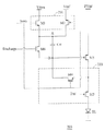
図2は、本発明の実施例に基づいた画素駆動回路を表している。画素駆動回路200は、スレッショルド電圧と電力供給を補償することで、電力供給の電圧PVddがスキャン信号Scanによって制限されないことができる。画素駆動回路200は、蓄積コンデンサCst、転送回路210、駆動トランジスタM5、トランジスタM6と、スイッチング回路220を含む。
FIG. 2 shows a pixel driving circuit according to an embodiment of the present invention. The
転送回路210は、蓄積コンデンサCstの第1節点Aに接続され、データ信号Vdata、または基準信号Vrefを蓄積コンデンサCstの第1節点Aに転送する。基準信号Vrefは、定電圧信号であることができる。駆動トランジスタM5は、P型金属酸化膜半導体(PMOS)トランジスタであることができる。トランジスタM5のソース端子は、第1電圧PVddに接続される。トランジスタM5のゲート端子は、蓄積コンデンサCstの第2節点Bに接続される。更に具体的に言えば、第1電圧は、電力供給PVddである。スイッチング回路220は、トランジスタM5のドレイン端子に接続される。スイッチング回路220は、トランジスタM5をダイオードとして機能するように導くことで、第4トランジスタM4がオンになり次第、トランジスタM5がダイオード接続のトランジスタとなる。表示素子ELは、スイッチング回路220に接続される。好ましくは、表示素子ELは、エレクトロルミネセント素子である。また、表示素子ELの陰極は、第2電圧に接続される。更に具体的に言えば、第2電圧は、電圧VSS、または接地電圧である。
The
図2に示すように、転送回路210は、第1トランジスタM1と第2トランジスタM2を含み、第1トランジスタM1と第2トランジスタM2は、それぞれN型金属酸化膜半導体(NMOS)トランジスタとPMOSトランジスタである。第1トランジスタM1のドレイン端子は、データ信号Vdataを受け、第1トランジスタM1のゲート端子とソース端子は、蓄積コンデンサCstの第1スキャンラインScanと第1節点Aにそれぞれ接続される。第2トランジスタM2のソース端子は、基準信号Vrefを受ける。第2トランジスタM2のゲート端子とドレイン端子は、蓄積コンデンサCstのスキャンラインScanと第1節点Aにそれぞれ接続される。好ましくは、トランジスタM1とM2は、ポリシリコン薄膜トランジスタであり、より高い電流駆動能力を提供する。
As shown in FIG. 2, the
スキャンラインScanが高く引き上げられた時、転送回路210は、データ信号Vdataを蓄積コンデンサCstの第1節点Aに転送する。スキャンラインScanが低く引き下げられた時、転送回路210は、基準信号Vrefを蓄積コンデンサCstの第1節点Aに転送する。
When the scan line Scan is pulled high, the
スイッチング回路220は、第3トランジスタM3と第4トランジスタM4を含む。図2に示すように、第3トランジスタM3は、PMOSトランジスタであり、第4トランジスタM4は、NMOSトランジスタである。第3トランジスタM3のドレイン端子は、表示素子ELの陽極に接続され、第3トランジスタM3のゲート端子とソース端子は、発光信号Emiと駆動トランジスタM5にそれぞれ接続される。第4トランジスタM4は、駆動トランジスタM5と第3トランジスタM3に接続されたソース端子を含む。第4トランジスタM4のドレイン端子は、蓄積コンデンサCstの第2節点B、トランジスタM6のソース端子と、駆動トランジスタM5のゲート端子に接続される。第4トランジスタM4のゲート端子は、スキャンラインScanに接続される。好ましくは、M3とM4は、ポリシリコン薄膜トランジスタであり、より高い電流駆動能力を提供する。
The
スキャンラインScanが高く引き上げられた時、スイッチング回路220の第4トランジスタM4は、トランジスタM5をダイオードとして機能するように導き、第4トランジスタM4がオンになった時、ダイオード接続のトランジスタとなる。
When the scan line Scan is pulled high, the fourth transistor M4 of the
トランジスタM6のドレイン端子は、蓄積コンデンサCstの第1節点Aに接続される。トランジスタM6のゲート端子は、放電信号Dischargeに接続される。トランジスタM6のソース端子は、蓄積コンデンサCstの第2節点B、トランジスタM4のドレイン端子と、駆動トランジスタM5のゲート端子に接続される。 The drain terminal of the transistor M6 is connected to the first node A of the storage capacitor Cst. The gate terminal of the transistor M6 is connected to the discharge signal Discharge. The source terminal of the transistor M6 is connected to the second node B of the storage capacitor Cst, the drain terminal of the transistor M4, and the gate terminal of the driving transistor M5.
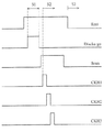
図3は、図2に示す画素駆動回路200の発光信号Emi、放電信号Discharge、スキャンラインScanと、水平クロック信号CKH1、CKH2と、CKH3の信号のタイミング図である。画素駆動回路の先の発光モードでは、放電信号Dischargeが高く引き上げられ、発光信号Emiが高く維持されている時、図2の画素駆動回路200は、放電モードS1にある。放電モードS1では、トランジスタM6は、オンにされ、高レベルの基準信号Vrefが蓄積コンデンサCstの第1節点Aと第2節点Bに入力される。よって、蓄積コンデンサCstに保存された電荷は、この放電モードで放電される。蓄積コンデンサCstの放電は、続くステップで正常な操作を確保する。
FIG. 3 is a timing diagram of the light emission signal Emi, the discharge signal Discharge, the scan line Scan, and the horizontal clock signals CKH1, CKH2, and CKH3 of the
蓄積コンデンサCstの放電に続いて、スキャン信号Scanは、高く引き上げられ、続いて、画素駆動回路200がデータロードモードS2に入る。スキャン信号Scanが高く引き上げられた時、第1トランジスタM1と第4トランジスタM4は、オンにされ、第2トランジスタM2とトランジスタM6は、オフにされる。第1トランジスタM1と第4トランジスタM4がオンにされることから、蓄積コンデンサCstの第1節点Aの電圧は、データ信号Vdataの電圧に等しく、駆動トランジスタM5のスレッショルド電圧は、Vthである。よって、蓄積コンデンサ内に保存された電圧は、Vdata−(PVdd−Vth)である。
Following the discharge of the storage capacitor Cst, the scan signal Scan is pulled high, and then the
スキャン信号Scanが低く引き下げられた時、データロードモードS2は、終了する。発光信号Emiが低く引き下げられた時、画素駆動回路200は、発光モードS3に入る。スキャンライン信号Scanが低いことから、第2トランジスタM2は、オンにされ、蓄積コンデンサCstの第1節点Aの電圧は、基準信号Vrefとなる。蓄積コンデンサ内に保存された電圧が直ちに変わることができないことから、蓄積コンデンサCstの第2節点Bの電圧は、Vref−[Vdata−(PVdd−Vth)]となる。表示素子に流れる電流は、(Vsg−Vth)2に比例し、(Vdata−Vref)2にも比例する。よって、表示素子ELに流れる電流は、駆動トランジスタM5のスレッショルド電圧Vthと電力供給PVddにも無関係である。画素駆動回路の操作は、連続的に繰り返し、画素の発光を制御する。
When the scan signal Scan is pulled low, the data load mode S2 ends. When the light emission signal Emi is pulled low, the
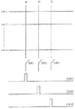
図4は、水平クロック信号CKH1、CKH2と、CKH3を用いてデータを赤R、緑Gと、青Bの信号ラインにそれぞれロードしたAMOLEDディスプレイを表している。列1、列2、...または列n(row1、row2、...またはrown)のスキャンライン信号Scanが高い時、データロードモードS2では、水平クロック信号CKH1、CKH2と、CKH3は、スイッチSW1、SW2と、SW3を順次にそれぞれオンにし、データが赤R、緑Gと、青Bの信号ラインに順次にロードされる。
FIG. 4 shows an AMOLED display in which data is loaded onto the red R, green G, and blue B signal lines using horizontal clock signals CKH1, CKH2, and CKH3, respectively.
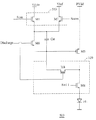
図5は、本発明のもう1つの実施例に基づいた画素駆動回路500を表している。画素駆動回路500は、スレッショルド電圧と電力供給を補償することで、電力供給の電圧PVddがスキャン信号Scanによって制限されないことができる。画素駆動回路500は、図5のトランジスタM7とM8がNMOSトランジスタであり、図2の第2トランジスタM2と第3トランジスタM3がPMOSトランジスタであることを除いて、画素駆動回路200に似ている。図5のトランジスタM7のゲート端子は、反(inverse)スキャンライン信号ScanXに接続される。反スキャンライン信号ScanXの位相(phase)は、スキャンライン信号Scanの位相の逆である。
FIG. 5 illustrates a
図6は、図5に示す画素駆動回路500の発光信号Emi、放電信号Discharge、スキャンライン信号Scan、反スキャンライン信号ScanXと、水平クロック信号CKH1、CKH2と、CKH3の信号のタイミング図である。画素駆動回路の先の発光モードでは、放電信号Dischargeが低く引き下げられ、発光信号Emiが低く維持されている時、図5の画素駆動回路500は、放電モードS1で操作される。放電モードS1では、トランジスタM6は、オンにされ、高レベルの基準信号Vrefが蓄積コンデンサCstの第1節点Aと第2節点Bに入力される。よって、蓄積コンデンサCstに保存された電荷は、この放電モードで放電される。蓄積コンデンサCstの放電は、続くステップで正常な操作を確保する。
FIG. 6 is a timing diagram of the light emission signal Emi, the discharge signal Discharge, the scan line signal Scan, the anti-scan line signal ScanX, and the horizontal clock signals CKH1, CKH2, and CKH3 of the
図7は、画像表示システムのもう1つの実施例を概略的に表しており、この場合、表示パネル400、または電子装置600として実施される。図7に示すように、表示パネル400は、図2の画素駆動回路200を含む。表示パネル400は、さまざまな電子装置(この場合、電子装置600)の一部を形成することができる。一般的に、電子装置600は、表示パネル400と電力供給700を含むことができる。また、電力供給700は、表示パネル400に選択的に接続され、表示パネル400に電力を提供する。電子装置600は、例えば、携帯電話、デジタルカメラ、PDA、ノート型パソコン、デスクトップ型パソコン、テレビ、または携帯型DVDプレーヤーであることができる。
FIG. 7 schematically illustrates another embodiment of the image display system, which is implemented as a
図5の操作は、図2の操作と似ている。よって、図5の表示素子ELに流れる電流は、(Vsg−Vth)2に比例し、(Vdata−Vref)2にも比例する。よって、図5の表示素子ELに流れる電流は、駆動トランジスタM5のスレッショルド電圧Vthと電力供給PVddにも無関係である。画素駆動回路の操作は、連続的に繰り返し、画素の発光を制御する。 The operation of FIG. 5 is similar to the operation of FIG. Therefore, the current flowing through the display element EL in FIG. 5 is proportional to (Vsg−Vth) 2 and also proportional to (Vdata−Vref) 2 . Therefore, the current flowing through the display element EL in FIG. 5 is independent of the threshold voltage Vth of the drive transistor M5 and the power supply PVdd. The operation of the pixel driving circuit is continuously repeated to control the light emission of the pixel.
本発明の実施例の画素駆動回路200と500(図2と5)は、駆動トランジスタM5のスレッショルド電圧Vthと電力供給PVddにも無関係である。電力供給PVddとスキャンライン信号Scanは、互いに無関係である。よって、スキャンライン信号Scanの電圧範囲は、電力供給PVddの電圧範囲に制限されないことができ、その逆もまた同様である。
The
以上、本発明の好適な実施例を例示したが、これは本発明を限定するものではなく、本発明の精神及び範囲を逸脱しない限りにおいては、当業者であれば行い得る少々の変更や修飾を付加することは可能である。従って、本発明が保護を請求する範囲は、特許請求の範囲を基準とする。 The preferred embodiments of the present invention have been described above, but this does not limit the present invention, and a few changes and modifications that can be made by those skilled in the art without departing from the spirit and scope of the present invention. It is possible to add. Accordingly, the scope of the protection claimed by the present invention is based on the scope of the claims.
Vdd 電源
Cst 蓄積コンデンサ
Scan スキャンライン信号
ScanX 反スキャンライン信号
Vdata データ信号
EL 表示素子
PVdd 電力供給電圧
Vref 基準信号
Vth スレッショルド電圧
Discharge 放電信号
S1 放電モード
S2 データロードモード
S3 発光モード
Emi、Emi1 発光信号
210、510 転送回路
220、520 スイッチング回路
R、G、B 信号ライン
SW1、SW2、SW3 スイッチ
10、200、500 画素駆動回路
CKH1、CKH2と、CKH3 水平クロック信号
M1、M2、M3、M4、M5、M6、Mx、My トランジスタ
row1、row2、...rown 列1、列2、...列n
400 ディスプレイパネル
500 画素駆動回路
600 電子装置
Vdd power supply
Cst Storage capacitor Scan Scan line signal ScanX Anti-scan line signal Vdata Data signal EL Display element PVdd Power supply voltage Vref Reference signal Vth Threshold voltage Discharge Discharge signal S1 Discharge mode S2 Data load mode S3 Light emission mode Emi, Emi1
400
Claims (10)
第1節点と第2節点を有する蓄積コンデンサ、
放電信号に接続されたゲートを有し、前記第1節点と前記第2節点の間に接続され、第1期間の間、前記放電信号によってオンにされ、前記蓄積コンデンサを放電するトランジスタ、
前記蓄積コンデンサの前記第1節点に接続され、データ信号、または基準信号を前記蓄積コンデンサの前記第1節点に転送する転送回路、
第1定電位に接続された第1端子、前記蓄積コンデンサの第2節点に接続された第2端子と、駆動電流を出力する第3端子を有する駆動素子、および
前記駆動素子と表示素子の間に接続され、第2期間の間、前記駆動素子がダイオードとして操作するように導き、第3期間の間、前記駆動電流が前記表示素子に出力されるようにするスイッチング回路を含む画像表示システム。 An image display system including a pixel driving circuit, wherein the driving circuit includes:
A storage capacitor having a first node and a second node;
A transistor having a gate connected to a discharge signal, connected between the first node and the second node, turned on by the discharge signal during a first period, and discharging the storage capacitor;
A transfer circuit connected to the first node of the storage capacitor and transferring a data signal or a reference signal to the first node of the storage capacitor;
A driving element having a first terminal connected to the first constant potential, a second terminal connected to the second node of the storage capacitor, and a third terminal for outputting a driving current; and between the driving element and the display element An image display system including a switching circuit that is connected to and leads the drive element to operate as a diode during a second period and outputs the drive current to the display element during a third period.
第1スキャンラインに接続された第4端子、前記データ信号を受ける第5端子と、前記蓄積コンデンサの前記第1節点に接続された第6端子を有する第1トランジスタ、および
第1スキャンラインに接続された第7端子、前記基準信号を受ける第8端子と、前記蓄積コンデンサの前記第1節点に接続された第9端子を有する第2トランジスタを含む請求項1に記載のシステム。 The transfer circuit includes:
A fourth transistor connected to the first scan line, a fifth terminal for receiving the data signal, a first transistor having a sixth terminal connected to the first node of the storage capacitor, and connected to the first scan line The system of claim 1, further comprising: a second transistor having a seventh terminal connected, an eighth terminal receiving the reference signal, and a ninth terminal connected to the first node of the storage capacitor.
第1スキャンラインに接続された第4端子、前記データ信号を受ける第5端子と、前記蓄積コンデンサの前記第1節点に接続された第6端子を有する第1トランジスタ、および
第2スキャンラインに接続された第7端子、前記基準信号を受ける第8端子と、前記蓄積コンデンサの前記第1節点に接続された第9端子を有する第2トランジスタを含む請求項1に記載のシステム。 The transfer circuit includes:
A fourth terminal connected to the first scan line, a fifth terminal for receiving the data signal, a first transistor having a sixth terminal connected to the first node of the storage capacitor, and a second scan line The system of claim 1, further comprising: a second transistor having a seventh terminal connected, an eighth terminal receiving the reference signal, and a ninth terminal connected to the first node of the storage capacitor.
発光信号に接続された第4端子、前記表示素子に接続された第5端子と、前記駆動素子に接続された第6端子を有する第3トランジスタ、および
前記蓄積コンデンサの前記第2節点に接続された第7端子、第1スキャンラインに接続された第8端子と、前記駆動素子に接続された第9端子を有する第4トランジスタを含む請求項1に記載のシステム。 The switching circuit is
A fourth terminal connected to the light emitting signal, a fifth terminal connected to the display element, a third transistor having a sixth terminal connected to the driving element, and connected to the second node of the storage capacitor; The system of claim 1, further comprising a fourth transistor having a seventh terminal, an eighth terminal connected to the first scan line, and a ninth terminal connected to the drive element.
トランジスタに前記放電信号を供給することで前記トランジスタによって蓄積コンデンサを放電するステップ、
データ信号を前記蓄積コンデンサの第1端子内にロードするステップ、
前記駆動素子のゲート電圧を前記蓄積コンデンサの第2端子内にロードするステップ、
基準信号を前記蓄積コンデンサの前記第1端子内にロードするステップ、および
前記ロードしたデータ信号、前記ゲート電圧と、前記基準信号を前記駆動素子内に結合し、スレッショルド電圧と無関係の駆動電流を前記表示素子に提供するステップを含む表示素子の駆動方法。 A driving method of a display element having a driving element and a storage capacitor,
Discharging a storage capacitor by the transistor by supplying the discharge signal to the transistor;
Loading a data signal into the first terminal of the storage capacitor;
Loading the gate voltage of the drive element into the second terminal of the storage capacitor;
Loading a reference signal into the first terminal of the storage capacitor; and coupling the loaded data signal, the gate voltage, and the reference signal into the drive element to provide a drive current independent of a threshold voltage; A display element driving method including a step of providing to a display element.
Applications Claiming Priority (1)
| Application Number | Priority Date | Filing Date | Title |
|---|---|---|---|
| TW95116371 | 2006-05-09 |
Publications (1)
| Publication Number | Publication Date |
|---|---|
| JP2007304594A true JP2007304594A (en) | 2007-11-22 |
Family
ID=38684628
Family Applications (2)
| Application Number | Title | Priority Date | Filing Date |
|---|---|---|---|
| JP2007123022A Pending JP2007304594A (en) | 2006-05-09 | 2007-05-08 | Image display system and method for driving display elements |
| JP2007124163A Pending JP2007304598A (en) | 2006-05-09 | 2007-05-09 | Image display system |
Family Applications After (1)
| Application Number | Title | Priority Date | Filing Date |
|---|---|---|---|
| JP2007124163A Pending JP2007304598A (en) | 2006-05-09 | 2007-05-09 | Image display system |
Country Status (4)
| Country | Link |
|---|---|
| US (2) | US7817120B2 (en) |
| JP (2) | JP2007304594A (en) |
| KR (1) | KR20070109893A (en) |
| TW (1) | TWI371018B (en) |
Cited By (2)
| Publication number | Priority date | Publication date | Assignee | Title |
|---|---|---|---|---|
| JP4979772B2 (en) * | 2007-10-18 | 2012-07-18 | シャープ株式会社 | Current-driven display device |
| JP2021501368A (en) * | 2017-11-17 | 2021-01-14 | 深▲セン▼市▲華▼星光▲電▼半▲導▼体▲顕▼示技▲術▼有限公司 | AMOLED pixel drive circuit and its drive method |
Families Citing this family (53)
| Publication number | Priority date | Publication date | Assignee | Title |
|---|---|---|---|---|
| TWI371018B (en) * | 2006-05-09 | 2012-08-21 | Chimei Innolux Corp | System for displaying image and driving display element method |
| WO2009035588A1 (en) * | 2007-09-12 | 2009-03-19 | Corning Incorporated | Derivative sampled, fast settling time current driver |
| KR100893481B1 (en) * | 2007-11-08 | 2009-04-17 | 삼성모바일디스플레이주식회사 | Organic light emitting display device and driving method using the same |
| US20090201278A1 (en) * | 2008-02-13 | 2009-08-13 | Samsung Electronics Co., Ltd. | Unit pixels and active matrix organic light emitting diode displays including the same |
| US20090201235A1 (en) * | 2008-02-13 | 2009-08-13 | Samsung Electronics Co., Ltd. | Active matrix organic light emitting diode display |
| KR101404549B1 (en) * | 2008-02-15 | 2014-06-10 | 삼성디스플레이 주식회사 | Display device and driving method thereof |
| JP5359073B2 (en) * | 2008-07-09 | 2013-12-04 | ソニー株式会社 | Display device |
| KR101518324B1 (en) | 2008-09-24 | 2015-05-11 | 삼성디스플레이 주식회사 | Display device and driving method thereof |
| KR101008438B1 (en) * | 2008-11-26 | 2011-01-14 | 삼성모바일디스플레이주식회사 | Pixel and Organic Light Emitting Display Device |
| KR20110091998A (en) * | 2010-02-08 | 2011-08-17 | 삼성전기주식회사 | Organic light emitting display |
| KR20120019691A (en) | 2010-08-26 | 2012-03-07 | 삼성모바일디스플레이주식회사 | Display device |
| TWI424413B (en) * | 2010-12-28 | 2014-01-21 | Au Optronics Corp | Pixel circuit of an active matrix organic light-emitting diode display device |
| KR101894768B1 (en) * | 2011-03-14 | 2018-09-06 | 삼성디스플레이 주식회사 | An active matrix display and a driving method therof |
| US9053665B2 (en) * | 2011-05-26 | 2015-06-09 | Innocom Technology (Shenzhen) Co., Ltd. | Display device and control method thereof without flicker issues |
| TWI455096B (en) * | 2011-05-26 | 2014-10-01 | Innolux Corp | Display device and control method thereof |
| TWI438752B (en) * | 2011-05-26 | 2014-05-21 | Innolux Corp | Pixel structure and display system utilizing the same |
| CN102800273B (en) * | 2011-05-26 | 2015-01-21 | 群创光电股份有限公司 | Pixel structure and display system provided with same |
| KR101813192B1 (en) * | 2011-05-31 | 2017-12-29 | 삼성디스플레이 주식회사 | Pixel, diplay device comprising the pixel and driving method of the diplay device |
| TWI442365B (en) * | 2011-07-13 | 2014-06-21 | Innolux Corp | Display system |
| TWI444972B (en) * | 2011-07-29 | 2014-07-11 | Innolux Corp | Display system |
| KR101399159B1 (en) | 2011-12-01 | 2014-05-28 | 엘지디스플레이 주식회사 | Organic light-emitting display device |
| TWI451384B (en) * | 2011-12-30 | 2014-09-01 | Au Optronics Corp | Pixel structure, driving method thereof and self-emitting display using the same |
| US9117409B2 (en) * | 2012-03-14 | 2015-08-25 | Semiconductor Energy Laboratory Co., Ltd. | Light-emitting display device with transistor and capacitor discharging gate of driving electrode and oxide semiconductor layer |
| WO2014077200A1 (en) * | 2012-11-13 | 2014-05-22 | ソニー株式会社 | Display device, display device driving method, and signal output circuit |
| KR101973125B1 (en) * | 2012-12-04 | 2019-08-16 | 엘지디스플레이 주식회사 | Pixel circuit and method for driving thereof, and organic light emitting display device using the same |
| KR101950846B1 (en) * | 2012-12-20 | 2019-02-22 | 엘지디스플레이 주식회사 | Light emitting diode display device |
| KR102072795B1 (en) * | 2013-08-12 | 2020-02-04 | 삼성디스플레이 주식회사 | Organic light emitting display device and method for driving the same |
| CN103531149B (en) * | 2013-10-31 | 2015-07-15 | 京东方科技集团股份有限公司 | AC (alternating current)-driven pixel circuit, driving method and display device |
| CN104050916B (en) * | 2014-06-04 | 2016-08-31 | 上海天马有机发光显示技术有限公司 | The pixel compensation circuit of a kind of OLED and method |
| CN104064149B (en) * | 2014-07-07 | 2016-07-06 | 深圳市华星光电技术有限公司 | Image element circuit, the display floater possessing this image element circuit and display |
| KR102196908B1 (en) * | 2014-07-18 | 2020-12-31 | 삼성디스플레이 주식회사 | Organic light emitting display device and driving method thereof |
| TWI539422B (en) * | 2014-09-15 | 2016-06-21 | 友達光電股份有限公司 | Pixel architechture and driving method thereof |
| CN104252845B (en) | 2014-09-25 | 2017-02-15 | 京东方科技集团股份有限公司 | Pixel driving circuit, pixel driving method, display panel and display device |
| KR102274740B1 (en) * | 2014-10-13 | 2021-07-08 | 삼성디스플레이 주식회사 | Display device |
| CN104464616B (en) | 2014-10-28 | 2017-10-03 | 上海天马有机发光显示技术有限公司 | Image element circuit and its driving method, display panel |
| TWI556210B (en) | 2014-11-26 | 2016-11-01 | 鴻海精密工業股份有限公司 | Pixel unit and driving method thereof |
| TWI562119B (en) | 2014-11-26 | 2016-12-11 | Hon Hai Prec Ind Co Ltd | Pixel unit and driving method for driving the pixel unit |
| CN105702198B (en) * | 2014-11-26 | 2019-01-04 | 鸿富锦精密工业(深圳)有限公司 | Pixel unit and its driving method |
| CN105702197B (en) * | 2014-11-26 | 2018-07-06 | 鸿富锦精密工业(深圳)有限公司 | pixel unit and its driving method |
| CN105702199B (en) * | 2014-11-26 | 2018-09-07 | 鸿富锦精密工业(深圳)有限公司 | Pixel unit and its driving method |
| CN104537985B (en) * | 2015-01-19 | 2017-06-30 | 深圳市华星光电技术有限公司 | A kind of organic electroluminescence display panel and its voltage-drop compensation method |
| JP6653551B2 (en) | 2015-11-09 | 2020-02-26 | 株式会社ジャパンディスプレイ | Display device and display device driving method |
| CN106409198B (en) | 2016-11-24 | 2017-11-10 | 京东方科技集团股份有限公司 | A kind of method for detecting drive circuit |
| CN106611586B (en) * | 2017-03-08 | 2018-11-13 | 京东方科技集团股份有限公司 | Pixel-driving circuit, driving method, organic light emitting display panel and display device |
| CN107331351B (en) * | 2017-08-24 | 2023-08-29 | 京东方科技集团股份有限公司 | Pixel compensation circuit, driving method thereof, display panel and display device |
| CN207474028U (en) * | 2017-10-31 | 2018-06-08 | 昆山国显光电有限公司 | A kind of pixel circuit and display device |
| CN208488962U (en) * | 2018-08-06 | 2019-02-12 | 上海视涯信息科技有限公司 | A kind of pixel circuit and display device |
| CN109671394A (en) * | 2019-02-21 | 2019-04-23 | 深圳市华星光电半导体显示技术有限公司 | OLED pixel driving circuit and OLED display |
| CN111312170A (en) * | 2019-11-13 | 2020-06-19 | 武汉华星光电半导体显示技术有限公司 | Pixel driving circuit and display device |
| CN210378423U (en) * | 2019-11-29 | 2020-04-21 | 京东方科技集团股份有限公司 | Pixel driving circuit and display device |
| CN111564138B (en) * | 2020-06-10 | 2022-04-22 | 京东方科技集团股份有限公司 | Pixel circuit, driving method thereof, display panel and display device |
| CN112837656A (en) * | 2021-01-11 | 2021-05-25 | 武汉华星光电半导体显示技术有限公司 | Pixel driving circuit, display panel and driving method thereof |
| CN114023255A (en) * | 2021-11-22 | 2022-02-08 | 惠州视维新技术有限公司 | Drive circuit, drive device, and display device |
Citations (7)
| Publication number | Priority date | Publication date | Assignee | Title |
|---|---|---|---|---|
| JPH10319908A (en) * | 1997-04-14 | 1998-12-04 | Sarnoff Corp | Display pixel structure for active matrix organic light emitting diode (amoled), and data load/light emitting circuit therefor |
| JP2000221942A (en) * | 1999-01-29 | 2000-08-11 | Nec Corp | Organic el element driving device |
| JP2005091724A (en) * | 2003-09-17 | 2005-04-07 | Seiko Epson Corp | Electronic circuit, its driving method, optoelectronic device and electronic equipment |
| JP2005157244A (en) * | 2003-11-27 | 2005-06-16 | Samsung Sdi Co Ltd | Light emitting display device and display panel and driving method therefor |
| JP2005309150A (en) * | 2004-04-22 | 2005-11-04 | Seiko Epson Corp | Electronic circuit, its driving method, optoelectronic device, and electronic equipment |
| JP2006048041A (en) * | 2004-08-02 | 2006-02-16 | Toppoly Optoelectronics Corp | Pixel driving circuit with threshold voltage compensation |
| JP2007114426A (en) * | 2005-10-19 | 2007-05-10 | Sanyo Electric Co Ltd | Display device |
Family Cites Families (16)
| Publication number | Priority date | Publication date | Assignee | Title |
|---|---|---|---|---|
| TW466466B (en) * | 2000-06-21 | 2001-12-01 | Chi Mei Optoelectronics Corp | Driving circuit of thin film transistor light emitting display and the usage method thereof |
| JP2002244617A (en) * | 2001-02-15 | 2002-08-30 | Sanyo Electric Co Ltd | Organic el pixel circuit |
| US7061451B2 (en) * | 2001-02-21 | 2006-06-13 | Semiconductor Energy Laboratory Co., Ltd, | Light emitting device and electronic device |
| EP1262948B1 (en) * | 2001-05-22 | 2016-05-11 | LG Display Co., Ltd. | Circuit for driving display |
| JP2003177709A (en) * | 2001-12-13 | 2003-06-27 | Seiko Epson Corp | Pixel circuit for light emitting element |
| KR100408301B1 (en) * | 2001-12-31 | 2003-12-01 | 삼성전자주식회사 | Apparatus for driving a image display device and design method of image display apparatus |
| JP2003316315A (en) | 2002-04-23 | 2003-11-07 | Tohoku Pioneer Corp | Device and method to drive light emitting display panel |
| GB0307789D0 (en) * | 2003-04-04 | 2003-05-07 | Koninkl Philips Electronics Nv | Electroluminescent display devices |
| KR100560780B1 (en) * | 2003-07-07 | 2006-03-13 | 삼성에스디아이 주식회사 | Pixel circuit in OLED and Method for fabricating the same |
| KR100741961B1 (en) * | 2003-11-25 | 2007-07-23 | 삼성에스디아이 주식회사 | Pixel circuit in flat panel display device and Driving method thereof |
| GB2411758A (en) * | 2004-03-04 | 2005-09-07 | Seiko Epson Corp | Pixel circuit |
| KR100578812B1 (en) * | 2004-06-29 | 2006-05-11 | 삼성에스디아이 주식회사 | Light emitting display |
| KR100570774B1 (en) * | 2004-08-20 | 2006-04-12 | 삼성에스디아이 주식회사 | Memory managing methods for display data of a light emitting display |
| KR100646992B1 (en) * | 2005-09-13 | 2006-11-23 | 삼성에스디아이 주식회사 | Emission driver and organic light emitting display using the same |
| TWI371018B (en) * | 2006-05-09 | 2012-08-21 | Chimei Innolux Corp | System for displaying image and driving display element method |
| TW200811812A (en) * | 2006-08-16 | 2008-03-01 | Tpo Displays Corp | System for displaying image and driving method for organic light-emitting element |
-
2007
- 2007-05-01 TW TW096115466A patent/TWI371018B/en not_active IP Right Cessation
- 2007-05-08 US US11/801,162 patent/US7817120B2/en active Active
- 2007-05-08 JP JP2007123022A patent/JP2007304594A/en active Pending
- 2007-05-09 KR KR1020070045122A patent/KR20070109893A/en not_active Application Discontinuation
- 2007-05-09 JP JP2007124163A patent/JP2007304598A/en active Pending
- 2007-12-12 US US11/954,257 patent/US8111216B2/en active Active
Patent Citations (7)
| Publication number | Priority date | Publication date | Assignee | Title |
|---|---|---|---|---|
| JPH10319908A (en) * | 1997-04-14 | 1998-12-04 | Sarnoff Corp | Display pixel structure for active matrix organic light emitting diode (amoled), and data load/light emitting circuit therefor |
| JP2000221942A (en) * | 1999-01-29 | 2000-08-11 | Nec Corp | Organic el element driving device |
| JP2005091724A (en) * | 2003-09-17 | 2005-04-07 | Seiko Epson Corp | Electronic circuit, its driving method, optoelectronic device and electronic equipment |
| JP2005157244A (en) * | 2003-11-27 | 2005-06-16 | Samsung Sdi Co Ltd | Light emitting display device and display panel and driving method therefor |
| JP2005309150A (en) * | 2004-04-22 | 2005-11-04 | Seiko Epson Corp | Electronic circuit, its driving method, optoelectronic device, and electronic equipment |
| JP2006048041A (en) * | 2004-08-02 | 2006-02-16 | Toppoly Optoelectronics Corp | Pixel driving circuit with threshold voltage compensation |
| JP2007114426A (en) * | 2005-10-19 | 2007-05-10 | Sanyo Electric Co Ltd | Display device |
Cited By (4)
| Publication number | Priority date | Publication date | Assignee | Title |
|---|---|---|---|---|
| JP4979772B2 (en) * | 2007-10-18 | 2012-07-18 | シャープ株式会社 | Current-driven display device |
| US8344982B2 (en) | 2007-10-18 | 2013-01-01 | Sharp Kabushiki Kaisha | Current-driven display device |
| US8514161B2 (en) | 2007-10-18 | 2013-08-20 | Sharp Kabushiki Kaisha | Current-driven display device |
| JP2021501368A (en) * | 2017-11-17 | 2021-01-14 | 深▲セン▼市▲華▼星光▲電▼半▲導▼体▲顕▼示技▲術▼有限公司 | AMOLED pixel drive circuit and its drive method |
Also Published As
| Publication number | Publication date |
|---|---|
| JP2007304598A (en) | 2007-11-22 |
| TWI371018B (en) | 2012-08-21 |
| US20070262931A1 (en) | 2007-11-15 |
| US8111216B2 (en) | 2012-02-07 |
| US7817120B2 (en) | 2010-10-19 |
| KR20070109893A (en) | 2007-11-15 |
| TW200802282A (en) | 2008-01-01 |
| US20080088547A1 (en) | 2008-04-17 |
Similar Documents
| Publication | Publication Date | Title |
|---|---|---|
| US7817120B2 (en) | System for displaying image and driving display element method | |
| US10878754B2 (en) | Organic light emitting display device including a maintain transistor | |
| CN101075410B (en) | Image display system and method for driving display assembly | |
| JP4398413B2 (en) | Pixel drive circuit with threshold voltage compensation | |
| JP5080733B2 (en) | Display device and driving method thereof | |
| US8009125B2 (en) | Organic electroluminescent display device | |
| US9293082B2 (en) | Organic light-emitting diode display | |
| KR101080351B1 (en) | Display device and driving method thereof | |
| JP5078236B2 (en) | Display device and driving method thereof | |
| KR100602352B1 (en) | Pixel and Light Emitting Display Using The Same | |
| JP5063769B2 (en) | Display device | |
| US8044891B2 (en) | Systems and methods for providing threshold voltage compensation of pixels | |
| US8130183B2 (en) | Scan driver and scan signal driving method and organic light emitting display using the same | |
| WO2016074359A1 (en) | Pixel circuit, organic electroluminescence display panel, and display device and driving method therefor | |
| JP5143499B2 (en) | Image display system | |
| KR101058107B1 (en) | Pixel circuit and organic light emitting display device using the same | |
| US11222587B2 (en) | Pixel circuit, display device, driving method of pixel circuit, and electronic apparatus | |
| US10049621B2 (en) | Organic light emitting display device with increased luminance uniformity | |
| EP1857998A1 (en) | System for displaying image and driving display element method | |
| US20210012718A1 (en) | Pixel and display device having the same | |
| JP2006243740A (en) | Display device and drive method thereof | |
| CN112908255A (en) | Pixel driving circuit, driving method thereof, display panel and display device |
Legal Events
| Date | Code | Title | Description |
|---|---|---|---|
| A621 | Written request for application examination |
Free format text: JAPANESE INTERMEDIATE CODE: A621 Effective date: 20100330 |
|
| A131 | Notification of reasons for refusal |
Free format text: JAPANESE INTERMEDIATE CODE: A131 Effective date: 20120221 |
|
| A977 | Report on retrieval |
Free format text: JAPANESE INTERMEDIATE CODE: A971007 Effective date: 20120222 |
|
| A02 | Decision of refusal |
Free format text: JAPANESE INTERMEDIATE CODE: A02 Effective date: 20120710 |