JP2007288062A - Terminal device, and method of connecting thereof - Google Patents
Terminal device, and method of connecting thereof Download PDFInfo
- Publication number
- JP2007288062A JP2007288062A JP2006115946A JP2006115946A JP2007288062A JP 2007288062 A JP2007288062 A JP 2007288062A JP 2006115946 A JP2006115946 A JP 2006115946A JP 2006115946 A JP2006115946 A JP 2006115946A JP 2007288062 A JP2007288062 A JP 2007288062A
- Authority
- JP
- Japan
- Prior art keywords
- tape
- terminal
- terminals
- substrate
- glass
- Prior art date
- Legal status (The legal status is an assumption and is not a legal conclusion. Google has not performed a legal analysis and makes no representation as to the accuracy of the status listed.)
- Pending
Links
Images
Classifications
-
- H—ELECTRICITY
- H05—ELECTRIC TECHNIQUES NOT OTHERWISE PROVIDED FOR
- H05K—PRINTED CIRCUITS; CASINGS OR CONSTRUCTIONAL DETAILS OF ELECTRIC APPARATUS; MANUFACTURE OF ASSEMBLAGES OF ELECTRICAL COMPONENTS
- H05K3/00—Apparatus or processes for manufacturing printed circuits
- H05K3/36—Assembling printed circuits with other printed circuits
- H05K3/361—Assembling flexible printed circuits with other printed circuits
-
- H—ELECTRICITY
- H01—ELECTRIC ELEMENTS
- H01L—SEMICONDUCTOR DEVICES NOT COVERED BY CLASS H10
- H01L2924/00—Indexing scheme for arrangements or methods for connecting or disconnecting semiconductor or solid-state bodies as covered by H01L24/00
- H01L2924/0001—Technical content checked by a classifier
- H01L2924/0002—Not covered by any one of groups H01L24/00, H01L24/00 and H01L2224/00
-
- H—ELECTRICITY
- H05—ELECTRIC TECHNIQUES NOT OTHERWISE PROVIDED FOR
- H05K—PRINTED CIRCUITS; CASINGS OR CONSTRUCTIONAL DETAILS OF ELECTRIC APPARATUS; MANUFACTURE OF ASSEMBLAGES OF ELECTRICAL COMPONENTS
- H05K1/00—Printed circuits
- H05K1/02—Details
- H05K1/11—Printed elements for providing electric connections to or between printed circuits
- H05K1/117—Pads along the edge of rigid circuit boards, e.g. for pluggable connectors
-
- H—ELECTRICITY
- H05—ELECTRIC TECHNIQUES NOT OTHERWISE PROVIDED FOR
- H05K—PRINTED CIRCUITS; CASINGS OR CONSTRUCTIONAL DETAILS OF ELECTRIC APPARATUS; MANUFACTURE OF ASSEMBLAGES OF ELECTRICAL COMPONENTS
- H05K2201/00—Indexing scheme relating to printed circuits covered by H05K1/00
- H05K2201/06—Thermal details
- H05K2201/068—Thermal details wherein the coefficient of thermal expansion is important
-
- H—ELECTRICITY
- H05—ELECTRIC TECHNIQUES NOT OTHERWISE PROVIDED FOR
- H05K—PRINTED CIRCUITS; CASINGS OR CONSTRUCTIONAL DETAILS OF ELECTRIC APPARATUS; MANUFACTURE OF ASSEMBLAGES OF ELECTRICAL COMPONENTS
- H05K2201/00—Indexing scheme relating to printed circuits covered by H05K1/00
- H05K2201/09—Shape and layout
- H05K2201/09209—Shape and layout details of conductors
- H05K2201/09654—Shape and layout details of conductors covering at least two types of conductors provided for in H05K2201/09218 - H05K2201/095
- H05K2201/09781—Dummy conductors, i.e. not used for normal transport of current; Dummy electrodes of components
-
- H—ELECTRICITY
- H05—ELECTRIC TECHNIQUES NOT OTHERWISE PROVIDED FOR
- H05K—PRINTED CIRCUITS; CASINGS OR CONSTRUCTIONAL DETAILS OF ELECTRIC APPARATUS; MANUFACTURE OF ASSEMBLAGES OF ELECTRICAL COMPONENTS
- H05K2203/00—Indexing scheme relating to apparatus or processes for manufacturing printed circuits covered by H05K3/00
- H05K2203/02—Details related to mechanical or acoustic processing, e.g. drilling, punching, cutting, using ultrasound
- H05K2203/0278—Flat pressure, e.g. for connecting terminals with anisotropic conductive adhesive
-
- H—ELECTRICITY
- H05—ELECTRIC TECHNIQUES NOT OTHERWISE PROVIDED FOR
- H05K—PRINTED CIRCUITS; CASINGS OR CONSTRUCTIONAL DETAILS OF ELECTRIC APPARATUS; MANUFACTURE OF ASSEMBLAGES OF ELECTRICAL COMPONENTS
- H05K2203/00—Indexing scheme relating to apparatus or processes for manufacturing printed circuits covered by H05K3/00
- H05K2203/16—Inspection; Monitoring; Aligning
- H05K2203/166—Alignment or registration; Control of registration
Landscapes
- Engineering & Computer Science (AREA)
- Manufacturing & Machinery (AREA)
- Microelectronics & Electronic Packaging (AREA)
- Combinations Of Printed Boards (AREA)
- Multi-Conductor Connections (AREA)
- Structure Of Printed Boards (AREA)
Abstract
Description
本発明は、基材よりも熱膨張率が大きいテープ基板に複数並設されたテープ側端子を備えた端子装置およびその接続方法に関する。 The present invention relates to a terminal device provided with a plurality of tape-side terminals arranged in parallel on a tape substrate having a thermal expansion coefficient larger than that of a base material, and a connection method thereof.
従来、例えば平面表示装置としての液晶表示装置などにおいては、平面表示素子としての液晶パネルである液晶セルに画素がマトリクス状に形成され、これら画素を駆動するスイッチング素子としての薄膜トランジスタ(TFT)が、これら薄膜トランジスタの駆動用のドライバICが実装されたテープ基板としてのポリイミドテープなどの可撓性を有するテープキャリアパッケージ(Tape Carrier Package、TCP)を介して、各種回路が形成された基板に、いわゆるアウタリードボンディング(Outer Lead Bonding、OBL)により電気的かつ機械的に接続される。 Conventionally, for example, in a liquid crystal display device as a flat display device, pixels are formed in a matrix in a liquid crystal cell that is a liquid crystal panel as a flat display element, and a thin film transistor (TFT) as a switching element that drives these pixels, A so-called outer layer is formed on a substrate on which various circuits are formed via a tape carrier package (TCP) having flexibility such as a polyimide tape as a tape substrate on which a driver IC for driving these thin film transistors is mounted. Electrically and mechanically connected by lead bonding (OBL).
すなわち、液晶セルを構成する基材としてのガラス基板側には、例えばITOなどにより基材側端子であるガラス側端子が複数並設され、テープキャリア側には、例えば銅などによりテープ側端子が複数並設され、これらガラス側端子と、テープ側端子とを対向させて異方性導電膜すなわちACF(Anisotropic Conductive Film)により熱圧着することで、両端子のそれぞれが電気的かつ機械的に接続される。 That is, on the glass substrate side as a base material constituting the liquid crystal cell, a plurality of glass side terminals which are base material side terminals such as ITO are arranged in parallel, and on the tape carrier side, for example, the tape side terminal is formed of copper or the like. A plurality of these terminals are juxtaposed, and the glass-side terminal and the tape-side terminal are opposed to each other, and the terminals are electrically and mechanically connected by thermocompression bonding using an anisotropic conductive film, ie, ACF (Anisotropic Conductive Film). Is done.
ところで、液晶セルのガラス基板と、ポリイミドテープなどのテープ基板とでは、熱膨張率が異なり、熱圧着により両端子を接続する際に、テープ基板がガラス基板よりも大きく延びる。このため、接続前のテープ側端子には、この延びの差を予め考慮してピッチが設定された、いわゆる縮小補正が施されており、熱圧着時にガラス側端子のピッチとテープ側端子のピッチとが等しくなるように構成されている(例えば、特許文献1参照。)。
しかしながら、上述の端子装置では、全てのテープ側端子が縮小補正されているため、接続前のテープ側端子をガラス側端子に対して位置合わせすなわちアライメントの際に、作業者がモニタなどで接続部をモニタリングしながらテープ基板の延びを考慮してテープ側端子の配置を決定しなければならない。すなわち、テープ側端子の全てをガラス側端子に正確に接続するためには、全てのテープ側端子の位置をガラス側端子に対してずれた位置となるように配置しなければならず、正確なアライメント作業に経験や時間を要するなど、アライメントが容易でないという問題点を有している。 However, in the terminal device described above, since all tape side terminals are reduced and corrected, the operator can use a monitor or the like to connect the tape side terminals before connection to the glass side terminals, that is, when alignment is performed. It is necessary to determine the arrangement of the tape side terminals in consideration of the extension of the tape substrate while monitoring. That is, in order to accurately connect all the tape side terminals to the glass side terminals, the positions of all the tape side terminals must be arranged so as to be shifted from the glass side terminals. There is a problem that alignment is not easy, for example, the alignment work requires experience and time.
本発明は、このような点に鑑みなされたもので、基材側端子とテープ側端子の一部とを容易かつ確実に接続できる端子装置およびその接続方法を提供することを目的とする。 This invention is made | formed in view of such a point, and it aims at providing the terminal device which can connect a base material side terminal and some tape side terminals easily and reliably, and its connection method.
本発明は、基材と、この基材上に複数並設された基材側端子と、前記基材よりも熱膨張率が大きいテープ基板と、前記基材側端子に対応して前記テープ基板に複数並設されたテープ側端子とを具備し、前記テープ側端子は、一の前記基材側端子と位置合わせ可能な位置合わせ用端子と、この位置合わせ用端子を一の前記基材側端子と位置合わせした状態で熱圧着による前記テープ基板の膨張によって他の前記基材側端子と電気的かつ機械的に接続される接続端子とを備えているものである。 The present invention relates to a base material, a plurality of base material side terminals arranged side by side on the base material, a tape substrate having a larger coefficient of thermal expansion than the base material, and the tape substrate corresponding to the base material side terminal. A plurality of tape-side terminals arranged side by side, the tape-side terminals being aligned with one of the substrate-side terminals, and the alignment terminal being connected to one of the substrate-side terminals A connection terminal that is electrically and mechanically connected to the other base material side terminal by expansion of the tape substrate by thermocompression bonding in a state of being aligned with the terminal.
そして、基材よりも熱膨張率が大きいテープ基板に複数並設したテープ側端子に、一の基材側端子と位置合わせ可能な位置合わせ用端子と、この位置合わせ用端子を一の基材側端子と位置合わせした状態で熱圧着によりテープ基板が膨張することで他の基材側端子と電気的かつ機械的に接続される接続端子とを設ける。 And, a plurality of tape side terminals arranged in parallel on a tape substrate having a larger coefficient of thermal expansion than the base material, an alignment terminal that can be aligned with one base material side terminal, and this positioning terminal as one base material When the tape substrate is expanded by thermocompression bonding in alignment with the side terminal, a connection terminal electrically and mechanically connected to the other base material side terminal is provided.
本発明によれば、テープ側端子の一部を基材側端子の一部との位置合わせ用の位置合わせ用端子として利用し、基材側端子とテープ側端子の接続端子とを容易かつ確実に接続できる。 According to the present invention, a part of the tape-side terminal is used as an alignment terminal for alignment with a part of the base-side terminal, and the base-side terminal and the connection terminal of the tape-side terminal can be easily and reliably. Can be connected.
以下、本発明の一実施の形態の構成を図1および図2を参照して説明する。 Hereinafter, the configuration of an embodiment of the present invention will be described with reference to FIG. 1 and FIG.
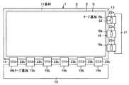
図2に平面表示装置としての液晶表示装置の一部を示し、この図2において、1は平面表示素子としてのアクティブマトリクス型の液晶表示素子すなわち液晶セルである。この液晶セル1は、第1の基板としてのアレイ基板2と第2の基板としての対向基板3と、これらアレイ基板2および対向基板3の間に挟持されて保持された図示しない液晶層とを有し、この液晶層の周囲にて基板2,3が図示しないシール剤により貼着されて液晶層が保持されている。そして、この液晶表示パネル2の中央部には、画像表示が可能な画像表示領域である矩形状の有効表示部5が設けられている。この有効表示部5には、図示しない複数の画素が液晶セル1の縦方向および横方向のそれぞれに沿ったマトリクス状に配置されている。
FIG. 2 shows a part of a liquid crystal display device as a flat display device. In FIG. 2, reference numeral 1 denotes an active matrix type liquid crystal display element as a flat display element, that is, a liquid crystal cell. The liquid crystal cell 1 includes an
アレイ基板2は、透光性を有する基材としての絶縁基板であるガラス基板11を備えており、このガラス基板11の一主面である内表面には、図示しない信号線と走査線とが互いに略直交するように配置されている。さらに、これら走査線および信号線にて仕切られて囲まれた各領域のそれぞれに有効表示部5の画素が位置している。また、これら画素のそれぞれには、スイッチング素子としての薄膜トランジスタ(TFT)と、画素電極とのそれぞれが設けられている。これら画素電極は、同一画素内の薄膜トランジスタに電気的に接続され、この薄膜トランジスタにて制御される。
The
さらに、ガラス基板11は、液晶セル1の有効表示部5から一側縁と両端縁とがそれぞれ突出し、この突出した一側縁と一端縁とが、それぞれ細長矩形状の額縁部である接続部13,14となっている。これら接続部13,14には、液晶セル1の有効表示部5の一側縁および一端縁からそれぞれ引き出された引き出し線群である図1(a)および図1(b)に示す複数の基材側端子としてのガラス側端子15a,15b(以下、これらガラス側端子15a,15bのいずれか、あるいは全体をガラス側端子15とすることがある)が並設されている。そして、これらガラス側端子15a,15bは、図2に示すテープ基板としてのテープキャリアパッケージ(Tape Carrier Package、以下TCPという)16a,16bを介して、接続側基板としてのゲート基板であるゲートPCB(Print Circuit Board)17と、接続側基板としてのソース基板であるソースPCB18とに電気的かつ機械的に接続されている。
Further, the glass substrate 11 has a connection portion in which one side edge and both end edges protrude from the
図1(a)および図1(b)に示すガラス側端子15は、例えばITOなどの導電性部材により形成されたOLB(Outer Lead Bonding)端子であり、互いに略等間隔に、例えば58μm〜80μmなどの狭ピッチに配置されている。
The glass-
図2に示すTCP16aは、例えばポリイミドテープなどの、可撓性を有しガラス基板11よりも熱膨張率が大きい合成樹脂などの部材により四角形状に形成され、図2に示す上下方向に複数、略等間隔に離間されて形成されている。また、各TCP16aは、ガラス基板11側に接続される複数のテープ側端子21aが並設されているとともに、液晶セル1の各薄膜トランジスタのゲート電極に電気的に接続されるゲート駆動用ICであるゲートドライバ22aがそれぞれ実装された、いわゆるCOF(Chip On FPC)テープである。
The TCP 16a shown in FIG. 2 is formed in a quadrangular shape by a member such as a synthetic resin having flexibility and a thermal expansion coefficient larger than that of the glass substrate 11 such as a polyimide tape, and a plurality of TCP 16a in the vertical direction shown in FIG. They are formed at substantially equal intervals. Each TCP 16a is a gate driving IC in which a plurality of tape-
TCP16bは、例えばポリイミドテープなどの、可撓性を有しガラス基板11よりも熱膨張率が大きい合成樹脂などの部材により四角形状に形成され、図2に示す左右方向に複数、略等間隔に離間されて形成されている。また、各TCP16bは、ガラス基板11側に接続される図1(a)および図1(b)に示す複数のテープ側端子21bが並設されているとともに、液晶セル1の各薄膜トランジスタのソース電極に電気的に接続されるソース駆動用ICであるソースドライバ22bがそれぞれ実装された、いわゆるCOFテープである。
The TCP 16b is formed in a quadrangular shape by a member such as a synthetic resin having flexibility and a coefficient of thermal expansion larger than that of the glass substrate 11 such as a polyimide tape. They are spaced apart. Each TCP 16b is provided with a plurality of
なお、以下、各TCP16a,16bのいずれか、あるいは全体をTCP16、各テープ側端子21a,21bのいずれか、あるいは全体をテープ側端子21、各ドライバ22a,22bのいずれか、あるいは全体をドライバ22とすることがある。
Hereinafter, any one of the
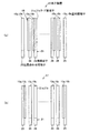
テープ側端子21は、例えば銅などの導電性部材により形成されたOLB端子であり、最外端に位置するテープ側端子21,21がそれぞれ最外端に位置するガラス側端子15,15との位置合わせ(アライメント)用の一対の位置合わせ用端子25,25となっているとともに、これら位置合わせ用端子25,25間に位置する他のテープ側端子21がそれぞれガラス側端子15との接続用の接続端子26となっている。
The
一対の位置合わせ用端子25,25は、接続端子26の両側方、すなわちテープ側端子21の最外端に位置している。また、これら位置合わせ用端子25,25は、最外端に位置するガラス側端子15,15との位置合わせ用にのみ用いられ、ドライバ22などとは電気的に接続されないダミー端子である。したがって、最外端に位置するガラス側端子15,15もまた、有効表示部5(図2)などに電気的に接続されないダミー端子とする。
The pair of
各接続端子26は、互いに略等間隔に配置され、最外端以外のガラス側端子15と、図示しない異方性導電膜(Anisotropic Conductive Film、以下ACFという)により熱圧着、すなわちACF接続される。ここで、これら接続端子26のピッチは、図1(a)に示す接続前の状態でガラス側端子15のピッチよりも狭く、図1(b)に示す接続後の状態でTCP16の熱膨張によりガラス側端子15のピッチと略等しくなるように、TCP16の材質の熱膨張率に対応していわゆる縮小補正が施されている。したがって、各位置合わせ用端子25は、このような縮小補正が施されておらず、隣接する接続端子26に対して、接続端子26,26のピッチよりも広い間隔で配置されている。
The
そして、ガラス基板11、ガラス側端子15、TCP16およびテープ側端子21により、端子装置27が構成されている。
The glass substrate 11, the
図2に戻って、ゲートPCB17は、ゲートドライバ22aを駆動するための図示しない各種回路が設けられ、TCP16aを介してそれぞれゲートドライバ22aと電気的に接続されている。同様に、ソースPCB18は、ソースドライバ22bを駆動するための図示しない各種回路が設けられ、TCP16bを介してそれぞれソースドライバ22bと電気的に接続されている。
Returning to FIG. 2, the
次に、上記一実施の形態の端子装置の接続方法を説明する。 Next, a method for connecting the terminal device according to the embodiment will be described.
ドライバ22を実装したTCP16のそれぞれの一端部を、画素および薄膜トランジスタなどを形成した液晶セル1の接続部13,14上に、図示しないACFを介在して配置する。
One end portion of each
このとき、作業者は、接続部13,14近傍を拡大する図示しない顕微鏡などに接続されたモニタなどによりモニタリングしつつ、図1(a)に示すように、最外端に位置するガラス側端子15,15を目安として、これらガラス側端子15,15上に位置合わせ用端子25,25を重ねるように位置合わせする。
At this time, the operator monitors with a monitor or the like connected to a microscope (not shown) that enlarges the vicinity of the
この状態で、TCP16をガラス基板11に熱圧着すると、TCP16の左右方向への熱膨張により、図1(b)に示すように、位置合わせ用端子25,25は最外端に位置するガラス側端子15,15の外方へとずれ、接続端子26はガラス側端子15と位置が重なり、これら接続端子26とガラス側端子15とが電気的に接続される。
In this state, when the
このように、上記一実施の形態によれば、ガラス基板11よりも熱膨張率が大きいTCP16に複数並設したテープ側端子21に、最外端のガラス側端子15,15と位置合わせ可能な位置合わせ用端子25,25を設けるとともに、位置合わせ用端子25,25を最外端のガラス側端子15,15と位置合わせした状態で熱圧着することでTCP16が熱膨張することにより他のガラス側端子15と電気的かつ機械的に接続される接続端子26を設けることで、テープ側端子21の一部を位置合わせ用端子25,25として利用し、TCP16の延びなどによるテープ側端子21の位置変化に対する作業者の経験や勘などに頼ることなく、ガラス側端子15と接続端子26とを容易かつ確実に接続できる。
As described above, according to the embodiment, the plurality of tape-
特に、液晶セル1などに用いられる端子装置では、上述のようにガラス側端子15のピッチが狭く設定されているので、接続端子26とガラス側端子15との位置がずれると短絡が生じたり所望の回路の接続できなかったりなどの問題が発生するおそれがあるため、上述のようにガラス側端子15とテープ側端子21とを容易に位置合わせして接続端子26とガラス側端子15とを確実に電気的かつ機械的に接続できることで、実装歩留まりおよび実装信頼性が向上する。
In particular, in the terminal device used for the liquid crystal cell 1 or the like, the pitch of the
また、位置合わせ用端子25,25は、接続状態で最外端のガラス側端子15,15と位置がずれるものの、位置合わせ用端子25,25と最外端のガラス側端子15,15とをダミー端子としておくことで、このようなずれにより電気的な問題が生じることはない。
In addition, although the
さらに、位置合わせ用端子25,25を接続端子26の両側方に配置、すなわちテープ側端子21の最外端とすることで、両方の位置合わせ用端子25によりテープ側端子21の幅方向を確認して接続時の接続端子26とガラス側端子15とを容易かつ確実に位置合わせできるとともに、TCP16が熱膨張により延びた際に、各位置合わせ用端子25がガラス側端子15の外方へとずれるので、他のガラス側端子15と接触してしまうこともない。
Furthermore, the
なお、上記一実施の形態では、ガラス基板11側とTCP16側とを電気的かつ機械的に接続する際に、上記構成を用いたが、例えば各PCB17,18を基材とし、これらPCB17,18にTCP16を電気的かつ機械的に接続する際に用いてもよい。
In the above-described embodiment, the above configuration is used when the glass substrate 11 side and the
また、位置合わせ用端子25は、一対設けたが、1つだけ設ける場合、あるいは3つ以上設ける場合でも、上記一実施の形態と同様の作用効果を奏することが可能であるとともに、位置合わせ用端子25を設ける位置も、TCP16の熱膨張時にガラス側端子15と接触しない位置などであれば、テープ側端子21の最外端でなくてもよい。
In addition, although a pair of
さらに、テープ基板は、TCP以外でも、例えばFPC(Flexible Print Circuit)、あるいはCOFなどでもよい。 Further, the tape substrate may be other than TCP, for example, FPC (Flexible Print Circuit) or COF.
そして、液晶表示装置用の配線としたが、任意の狭ピッチの接続に用いることが可能であることはいうまでもない。 And although it was set as the wiring for liquid crystal display devices, it cannot be overemphasized that it can be used for the connection of arbitrary narrow pitches.
11 基材としてのガラス基板
15a,15b 基材側端子としてのガラス側端子
16a,16b テープ基板としてのテープキャリアパッケージ
21a,21b テープ側端子
25 位置合わせ用端子
26 接続端子
27 端子装置
11 Glass substrate as base material
15a, 15b Glass side terminal as base side terminal
16a, 16b Tape carrier package as tape substrate
21a, 21b Tape side terminal
25 Positioning terminal
26 Connection terminal
27 Terminal equipment
Claims (4)
この基材上に複数並設された基材側端子と、
前記基材よりも熱膨張率が大きいテープ基板と、
前記基材側端子に対応して前記テープ基板に複数並設されたテープ側端子とを具備し、
前記テープ側端子は、
一の前記基材側端子と位置合わせ可能な位置合わせ用端子と、
この位置合わせ用端子を一の前記基材側端子と位置合わせした状態で熱圧着による前記テープ基板の膨張によって他の前記基材側端子と電気的かつ機械的に接続される接続端子とを備えている
ことを特徴とした端子装置。 A substrate;
A plurality of substrate-side terminals arranged side by side on the substrate;
A tape substrate having a larger coefficient of thermal expansion than the base material;
A plurality of tape side terminals arranged in parallel on the tape substrate corresponding to the base material side terminals,
The tape side terminal is
An alignment terminal that can be aligned with one of the substrate-side terminals;
A connection terminal that is electrically and mechanically connected to the other substrate side terminal by expansion of the tape substrate by thermocompression bonding in a state where the alignment terminal is aligned with the one substrate side terminal. A terminal device characterized by
ことを特徴とした請求項1記載の端子装置。 The terminal device according to claim 1, wherein a pair of the alignment terminals are provided at an outermost end of the tape side terminal.
前記テープ側端子の一部を位置合わせ用端子として、一の前記基材側端子と重なるように位置合わせし、
前記テープ基板を前記基材に対して熱圧着することにより前記テープ基板が膨張することで、前記テープ側端子の他部を接続端子として他の前記基材側端子と電気的かつ機械的に接続する
ことを特徴とした端子装置の接続方法。 A base material, base material side terminals arranged in parallel on the base material, a tape substrate having a larger coefficient of thermal expansion than the base material, and a plurality of juxtapositions on the tape substrate corresponding to the base material side terminals A terminal device connection method comprising a tape-side terminal,
A part of the tape side terminal is used as an alignment terminal, and is aligned so as to overlap the one base material side terminal,
The tape substrate expands by thermocompression bonding the tape substrate to the base material, so that the other part of the tape side terminal is electrically and mechanically connected to another base material side terminal as a connection terminal. A terminal device connection method characterized by:
ことを特徴とした請求項3記載の端子装置の接続方法。 The terminal device connection method according to claim 3, wherein the pair of tape-side terminals positioned at the outermost ends are used as the alignment terminals.
Priority Applications (3)
| Application Number | Priority Date | Filing Date | Title |
|---|---|---|---|
| JP2006115946A JP2007288062A (en) | 2006-04-19 | 2006-04-19 | Terminal device, and method of connecting thereof |
| TW96104276A TW200802768A (en) | 2006-04-19 | 2007-02-06 | Electric terminal device and method of connecting the same |
| US11/783,932 US8975756B2 (en) | 2006-04-19 | 2007-04-13 | Electric terminal device and method of connecting the same |
Applications Claiming Priority (1)
| Application Number | Priority Date | Filing Date | Title |
|---|---|---|---|
| JP2006115946A JP2007288062A (en) | 2006-04-19 | 2006-04-19 | Terminal device, and method of connecting thereof |
Publications (2)
| Publication Number | Publication Date |
|---|---|
| JP2007288062A true JP2007288062A (en) | 2007-11-01 |
| JP2007288062A5 JP2007288062A5 (en) | 2008-03-13 |
Family
ID=38618724
Family Applications (1)
| Application Number | Title | Priority Date | Filing Date |
|---|---|---|---|
| JP2006115946A Pending JP2007288062A (en) | 2006-04-19 | 2006-04-19 | Terminal device, and method of connecting thereof |
Country Status (3)
| Country | Link |
|---|---|
| US (1) | US8975756B2 (en) |
| JP (1) | JP2007288062A (en) |
| TW (1) | TW200802768A (en) |
Cited By (2)
| Publication number | Priority date | Publication date | Assignee | Title |
|---|---|---|---|---|
| JP2010243585A (en) * | 2009-04-01 | 2010-10-28 | Funai Electric Co Ltd | Liquid crystal module |
| JP2011128530A (en) * | 2009-12-21 | 2011-06-30 | Funai Electric Co Ltd | Assembling method of liquid crystal display apparatus, and chip mounted wiring substrate suitable for the method |
Families Citing this family (1)
| Publication number | Priority date | Publication date | Assignee | Title |
|---|---|---|---|---|
| US20160335835A1 (en) * | 2015-05-15 | 2016-11-17 | Wms Gaming Inc. | Gaming systems and electronic gaming machines with multi-display device arrangements |
Family Cites Families (7)
| Publication number | Priority date | Publication date | Assignee | Title |
|---|---|---|---|---|
| JP3039507B2 (en) * | 1998-03-06 | 2000-05-08 | 日本電気株式会社 | Liquid crystal display device and method of manufacturing the same |
| US6414741B2 (en) * | 2000-05-10 | 2002-07-02 | Kabushiki Kaisha Toshiba | Method of manufacturing flat-panel display device |
| JP2002032030A (en) | 2000-05-12 | 2002-01-31 | Seiko Epson Corp | Method for manufacturing electro-optic device, method for connecting terminal, electro-optic device and electronic apparatus |
| JP2002009412A (en) | 2000-06-26 | 2002-01-11 | Sanyo Electric Co Ltd | Connection method and connection structure of flexible board and display device |
| JP2003133677A (en) * | 2001-10-29 | 2003-05-09 | Advanced Display Inc | Pressure-contacting structure of flexible circuit board |
| JP2003249527A (en) | 2002-02-26 | 2003-09-05 | Seiko Epson Corp | Tape board, electronic components, electronic apparatus, and method of arranging terminal of tape board |
| JP2003295218A (en) * | 2002-04-04 | 2003-10-15 | Advanced Display Inc | Display device |
-
2006
- 2006-04-19 JP JP2006115946A patent/JP2007288062A/en active Pending
-
2007
- 2007-02-06 TW TW96104276A patent/TW200802768A/en unknown
- 2007-04-13 US US11/783,932 patent/US8975756B2/en active Active
Cited By (2)
| Publication number | Priority date | Publication date | Assignee | Title |
|---|---|---|---|---|
| JP2010243585A (en) * | 2009-04-01 | 2010-10-28 | Funai Electric Co Ltd | Liquid crystal module |
| JP2011128530A (en) * | 2009-12-21 | 2011-06-30 | Funai Electric Co Ltd | Assembling method of liquid crystal display apparatus, and chip mounted wiring substrate suitable for the method |
Also Published As
| Publication number | Publication date |
|---|---|
| US8975756B2 (en) | 2015-03-10 |
| TW200802768A (en) | 2008-01-01 |
| TWI338354B (en) | 2011-03-01 |
| US20070246836A1 (en) | 2007-10-25 |
Similar Documents
| Publication | Publication Date | Title |
|---|---|---|
| KR101195688B1 (en) | Flexible substrate and electric circuit structure | |
| JPWO2009004894A1 (en) | Display module, liquid crystal display device, and display module manufacturing method | |
| KR100848768B1 (en) | Board device and production method of display element | |
| KR100293982B1 (en) | LCD panel | |
| JP2000056285A (en) | Probe for inspecting liquid crystal display panel, device for inspecting liquid crystal display panel and method for inspecting | |
| KR20110064287A (en) | Borderless liquid crystal display device | |
| JP2008130803A (en) | Board device and substrate | |
| JP4740662B2 (en) | Display device and manufacturing method thereof | |
| JP3498448B2 (en) | Liquid crystal display | |
| US20080018849A1 (en) | Display element | |
| JP2007288062A (en) | Terminal device, and method of connecting thereof | |
| KR100885378B1 (en) | Liquid crystal display | |
| KR20040087452A (en) | Liquid crystal display module | |
| JP2002217237A (en) | Planar display device | |
| JP2005300920A (en) | Display device and liquid crystal display | |
| KR20150048364A (en) | Driving integrated circuit pad unit and flat display panel having the same | |
| JP3365305B2 (en) | Semiconductor chip, its mounting structure and liquid crystal display device | |
| KR100618580B1 (en) | Liquid crystal display device | |
| JP4413637B2 (en) | Display device | |
| JP2010050296A (en) | Tape carrier for semiconductor device, semiconductor device, and semiconductor module | |
| JP3575482B2 (en) | Display device | |
| KR20070044204A (en) | Liquid crystal display device | |
| WO2007142065A1 (en) | Display | |
| JP2003149666A (en) | Flexible wiring board | |
| JP2007011010A (en) | Display element |
Legal Events
| Date | Code | Title | Description |
|---|---|---|---|
| A521 | Written amendment |
Free format text: JAPANESE INTERMEDIATE CODE: A523 Effective date: 20080129 |
|
| A621 | Written request for application examination |
Free format text: JAPANESE INTERMEDIATE CODE: A621 Effective date: 20080129 |
|
| A131 | Notification of reasons for refusal |
Free format text: JAPANESE INTERMEDIATE CODE: A131 Effective date: 20080409 |
|
| A521 | Written amendment |
Free format text: JAPANESE INTERMEDIATE CODE: A523 Effective date: 20080604 |
|
| A02 | Decision of refusal |
Free format text: JAPANESE INTERMEDIATE CODE: A02 Effective date: 20081008 |