JP2007201166A - Redundant relief method for semiconductor integrated circuit device - Google Patents
Redundant relief method for semiconductor integrated circuit device Download PDFInfo
- Publication number
- JP2007201166A JP2007201166A JP2006017842A JP2006017842A JP2007201166A JP 2007201166 A JP2007201166 A JP 2007201166A JP 2006017842 A JP2006017842 A JP 2006017842A JP 2006017842 A JP2006017842 A JP 2006017842A JP 2007201166 A JP2007201166 A JP 2007201166A
- Authority
- JP
- Japan
- Prior art keywords
- circuit
- semiconductor integrated
- redundant
- power supply
- integrated circuit
- Prior art date
- Legal status (The legal status is an assumption and is not a legal conclusion. Google has not performed a legal analysis and makes no representation as to the accuracy of the status listed.)
- Withdrawn
Links
Images


Landscapes
- Tests Of Electronic Circuits (AREA)
- Semiconductor Integrated Circuits (AREA)
- Design And Manufacture Of Integrated Circuits (AREA)
Abstract
Description
本発明は半導体集積回路装置の冗長救済方法に関し、特に半ショート故障や半オープン故障を確実に検出して冗長救済を可能にする技術に関する。 The present invention relates to a redundancy repair method for a semiconductor integrated circuit device, and more particularly, to a technique that enables redundant repair by reliably detecting a half short failure or a half open failure.
従来、半導体集積回路装置の検査においては、機能(ファンクション)テストを実施することにより縮退故障、オープン故障、ショート故障を検出し、冗長救済可能な故障が存在する場合は、故障判定した回路をあらかじめ用意してある冗長救済回路と置換することで救済を実現している。冗長救済回路との置換方法としては、レーザや電圧の印加によりヒューズをカットする方法などがある。 Conventionally, in the inspection of semiconductor integrated circuit devices, stuck-at faults, open faults and short-circuit faults are detected by performing function tests. The repair is realized by replacing the prepared redundant repair circuit. As a replacement method with the redundant relief circuit, there is a method of cutting a fuse by applying a laser or a voltage.
特にメモリとロジックが混在したシステムLSIにおいては、通常DRAMにはあらかじめ冗長メモリセルが準備されているが、ロジック部については冗長ロジック部が搭載されていない。その不良救済を可能にするために、メモリに複数のロジック部を接続し、その1つのみを選択し、他のロジック部を切り離すフューズ回路などを備えたものがある。拡散工程後にロジック部を選択することにより、不良ロジック部を切り離して歩留まりを向上させることができる(例えば、特許文献1参照)。 In particular, in a system LSI in which memory and logic are mixed, a redundant memory cell is usually prepared in advance in a DRAM, but a redundant logic part is not mounted on a logic part. In order to make it possible to repair the defect, there are some which include a fuse circuit that connects a plurality of logic units to a memory, selects only one of them, and disconnects the other logic units. By selecting the logic part after the diffusion step, the defective logic part can be separated and the yield can be improved (for example, see Patent Document 1).
また、メモリの冗長救済を行うための不良メモリセルの発見を容易にする手法として、メモリセル電源配線を半導体記憶装置全体で利用される電源線から分離してメモリマット毎に個別化し、このメモリセル電源配線を選択的にメモリセル電流測定用の第2の電源配線に接続し、そこに種々の電圧を印加したときの電流を測定することにより、メモリブロック内のDC電流不良内容を解析可能にし、効率的にメモリセルの欠陥救済を施すものがある(例えば、特許文献2参照)。
しかしながら、従来の半導体集積回路装置の検査では、縮退故障、オープン故障、ショート故障チップの救済は可能だが、半ショート故障や半オープン故障のあるチップを確実に検出することはできず、後工程に行われる静止電源電流テストにおいて不良チップとして判定されていた。その結果、冗長救済可能な半ショート故障や半オープン故障チップが不良品として扱われ、歩留向上の障害となっていた。また、従来の半導体集積回路装置の冗長救済方法では、検査工程が別途必要であるために検査時間が増加し、専用の検査装置が別途必要であるために検査コストが増加するという問題があった。 However, conventional semiconductor integrated circuit device inspections can repair stuck-at faults, open faults, and short fault chips, but cannot reliably detect chips with half-short faults or half-open faults. It was determined as a defective chip in the quiescent power supply current test. As a result, half-short faults and half-open fault chips that can be redundantly remedied are treated as defective products, which is an obstacle to yield improvement. Further, the conventional redundancy repair method for a semiconductor integrated circuit device has a problem that inspection time is increased because a separate inspection process is required, and inspection cost is increased because a dedicated inspection device is required separately. .
本発明は、半導体集積回路装置の検査工程において、半ショート故障や半オープン故障を確実に検出して冗長救済を可能にする半導体集積回路装置の冗長救済方法を提供することを目的とする。 SUMMARY OF THE INVENTION An object of the present invention is to provide a redundant relief method for a semiconductor integrated circuit device capable of reliably detecting a half short failure and a half open failure in a semiconductor integrated circuit device inspection process and enabling redundancy relief.
本発明の冗長救済方法は、半導体集積回路装置に搭載された同一機能を有する被検査回路と冗長回路とがそれぞれ個別の電源に接続され、前記個別の電源における静止電源電流の測定値が異常であった場合に被検査回路を故障と判定し、故障と判定された被検査回路を冗長回路で置換するものである。上記構成によれば、被検査回路に半オープン故障や半ショート故障があった場合は静止電源電流が通常より多く流れるため、個別の電源における静止電源電流の測定値の異常を被検査回路の故障と判定することで、半ショート故障や半オープン故障を確実に検出して冗長救済を行うことが可能になる。 According to the redundant relief method of the present invention, a circuit to be inspected and a redundant circuit having the same function mounted on a semiconductor integrated circuit device are connected to individual power supplies, and the measured value of the quiescent power supply current in the individual power supply is abnormal. In such a case, the circuit to be inspected is determined to be faulty, and the circuit to be inspected determined to be faulty is replaced with a redundant circuit. According to the above configuration, if the circuit under test has a half open failure or a half short circuit failure, the quiescent power supply current flows more than usual. This makes it possible to reliably detect a half short failure or a half open failure and perform redundancy relief.
さらに本発明は、上記冗長救済方法において、被検査回路と冗長回路とがそれぞれ個別の接地に接続され、前記個別の電源と前記個別の接地との全ての組合せにおいて静止電源電流の測定を行うものである。上記構成によれば、個別の電源と個別の接地との全ての組合せにおいて静止電源電流の測定を行うため、個別の電源を増加させることなく検査対象回路と冗長回路を増やすことが可能となる。 Furthermore, the present invention provides the above redundancy remedy method in which the circuit under test and the redundant circuit are connected to separate grounds, and the static power supply current is measured in all combinations of the separate power supplies and the separate grounds. It is. According to the above configuration, the quiescent power supply current is measured in all combinations of individual power supplies and individual grounds, so that it is possible to increase the number of inspection target circuits and redundant circuits without increasing individual power supplies.
また本発明の半導体集積回路装置は、被検査回路と、冗長回路と、個別の電源の供給手段と、被検査回路を冗長回路で置換する冗長救済手段とを搭載し、上記冗長救済方法を実施可能に構成されたものである。上記構成によれば、半導体集積回路装置の個別の電源における静止電源電流の測定値の異常を被検査回路の故障と判定することで、半ショート故障や半オープン故障を確実に検出して冗長救済を行うことができる。 The semiconductor integrated circuit device according to the present invention includes a circuit to be tested, a redundant circuit, an individual power supply unit, and a redundant repair unit that replaces the circuit to be tested with a redundant circuit, and implements the above redundant repair method. It is configured to be possible. According to the above configuration, it is possible to reliably detect a half short-circuit failure or a half-open failure by determining an abnormality in the measured value of the quiescent power supply current in the individual power source of the semiconductor integrated circuit device as a failure of the circuit to be inspected. It can be performed.
さらに本発明は、上記構成の半導体集積回路装置において、複数の被検査回路に対して1個の冗長回路を対応させて構成されたものである。上記構成によれば、冗長回路を減らしてチップ面積を削減することができる。2個以上の被検査回路が故障と判定された場合は、冗長救済を行わず不良品扱いとする。 Further, according to the present invention, in the semiconductor integrated circuit device having the above-described configuration, one redundant circuit is associated with a plurality of circuits to be inspected. According to the above configuration, the redundant circuit can be reduced and the chip area can be reduced. When two or more circuits to be inspected are determined to be faulty, they are treated as defective products without performing redundancy relief.
さらに本発明は、上記構成の半導体集積回路装置において、静止電源電流を測定して測定値の異常を判定する異常電流検出回路を搭載したものである。さらに本発明は、上記構成の半導体集積回路装置において、異常電流検出回路に静止電源電流の測定値と比較する規格電流回路を備えたものである。上記構成によれば、静止電源電流の測定値と比較する規格電流回路を備えた異常電流検出回路を内部に搭載することにより、チップ面積は増加するが、外部の異常電流検出手段を用意する必要がなく、チップ単体で冗長救済を行うことが可能となる。 Further, according to the present invention, the semiconductor integrated circuit device having the above-described configuration is equipped with an abnormal current detection circuit that measures a quiescent power supply current and determines an abnormality in a measured value. Further, according to the present invention, in the semiconductor integrated circuit device configured as described above, the abnormal current detection circuit is provided with a standard current circuit for comparing with a measured value of the quiescent power supply current. According to the above configuration, an abnormal current detection circuit having a standard current circuit for comparison with a measured value of the quiescent power supply current is mounted inside, thereby increasing the chip area, but it is necessary to prepare an external abnormal current detection means Therefore, it becomes possible to carry out redundant relief with a single chip.
さらに本発明は、上記構成の半導体集積回路装置において、冗長救済手段としてヒューズ回路を用いたものである。上記構成によれば、故障と判定された被検査回路に対する電源供給経路をヒューズ回路を用いて切断し、冗長回路で置換することができるため、容易に冗長救済を行うことができる。 Furthermore, according to the present invention, a fuse circuit is used as a redundancy relief means in the semiconductor integrated circuit device having the above configuration. According to the above configuration, the power supply path to the circuit to be inspected determined to be faulty can be disconnected using the fuse circuit and replaced with the redundant circuit, so that redundant relief can be easily performed.
さらに本発明は、上記構成の半導体集積回路装置において、個別の電源における被検査回路と冗長回路の静止電源電流の測定値を比較する手段を備え、静止電源電流の測定値が大きい方の回路に対する電源供給経路を切断するものである。上記構成によれば、異常電流ではないが電流値の大きい回路に対してヒューズ回路を用いて電源供給経路を切断し、全体を低消費電力にすることができる。 Furthermore, the present invention provides a semiconductor integrated circuit device having the above-described configuration, comprising means for comparing measured values of the quiescent power supply current of the circuit under test and the redundant circuit in individual power supplies, for the circuit having the larger measured value of the quiescent power supply current. The power supply path is cut off. According to the above configuration, the power supply path can be cut using a fuse circuit for a circuit that is not an abnormal current but has a large current value, and the entire power consumption can be reduced.
さらに本発明は、上記構成の半導体集積回路装置において、冗長救済手段としてセレクタ回路等の接続切り換え手段を用いたものである。上記構成によれば、セレクタ回路等の接続切り換え手段により、故障と判定された被検査回路を冗長回路で置換することができるため、低消費電力にすることはできないが、より容易に冗長救済を行うことができる。 Further, according to the present invention, in the semiconductor integrated circuit device having the above configuration, connection switching means such as a selector circuit is used as redundancy relief means. According to the above configuration, since the circuit under test determined to be faulty can be replaced with a redundant circuit by the connection switching means such as the selector circuit, it is not possible to reduce the power consumption, but it is possible to easily repair the redundancy. It can be carried out.
さらに本発明は、上記構成の半導体集積回路装置において、故障と判定した被検査回路を冗長救済手段が自動的に冗長回路で置換するテストモードを備えたたものである。上記構成によれば、半導体集積回路装置をテストモードにすることにより、冗長救済手段により自動的に冗長救済が実施されるため、テスト時間を短縮し、テストコストを削減することができる。 The present invention further includes a test mode in which the redundant repair means automatically replaces the circuit under test determined to be faulty in the semiconductor integrated circuit device configured as described above. According to the above configuration, by setting the semiconductor integrated circuit device in the test mode, the redundant repair is automatically performed by the redundant repair means, so that the test time can be shortened and the test cost can be reduced.
本発明によれば、機能テストでは確実に検出することができなかった半オープン故障や半ショート故障を確実に検出して救済することが可能となる。これにより、従来は不良チップとして扱っていたものが救済処理され、歩留向上の効果が得られる。また、静止電源電流測定と異常検出を自動的に行うことにより、別工程での救済処理が不要となり、テスト時間を短縮し、テストコストを削減する効果が得られる。 According to the present invention, it is possible to reliably detect and relieve a half-open failure or a half-short failure that could not be reliably detected by the function test. As a result, what was conventionally handled as a defective chip is relieved, and the effect of yield improvement is obtained. Further, by automatically measuring the quiescent power supply current and detecting the abnormality, the relief process in a separate process becomes unnecessary, and the test time can be shortened and the test cost can be reduced.
(実施の形態1)
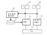
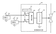
図1は本発明の実施の形態1に係る冗長救済方法を示す半導体集積回路装置の構成図である。図1において、101と102はそれぞれ半導体検査装置などから入力される個別の電源VS1とVS2、103は接地VSS、104は検査対象回路A、105は検査対象回路A104と同等の機能を持つ冗長回路B、106は検査対象回路A104と冗長回路B105の静止電源電流を個別に測定し検査対象回路A104の異常電流を検出する異常電流検出回路、107は異常電流検出回路106の結果から検査対象回路A104と冗長回路B105を置き換えるヒューズボックスである。
(Embodiment 1)
FIG. 1 is a configuration diagram of a semiconductor integrated circuit device showing a redundancy repair method according to
検査対象回路A104に半オープン故障や半ショート故障があった場合は、静止電源電流が通常規格値や冗長回路B105より多く流れる。この原理により、異常電流検出回路106で静止電源電流値を測定し、電流が通常規格値や冗長回路B105より多く流れた場合に冗長救済が必要と判定し、ヒューズボックス107においてフューズを切断することにより救済を行う。
When there is a half open fault or a half short fault in the circuit A104 to be inspected, the quiescent power supply current flows more than the normal standard value or the redundant circuit B105. Based on this principle, the quiescent power supply current value is measured by the abnormal
本実施の形態によれば、検査対象回路の静止電源電流が異常電流となった場合に異常検出信号を出力し、冗長回路を選択するように異常検出信号を用いてヒューズを切断することにより、冗長救済を自動的に行うことができる。 According to the present embodiment, when the static power supply current of the circuit to be inspected becomes an abnormal current, an abnormality detection signal is output, and the fuse is cut using the abnormality detection signal so as to select the redundant circuit, Redundant relief can be performed automatically.
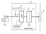
図4は異常電流検出回路106の構成例を示す図である。図4において、121は静止電源電流検査により冗長救済を実施するテストモード、122はテストモードでオンになるスイッチ、123は静止電源電流を異常と判定する検査規格電流、124は検査対象回路の静止電源電流値と検査規格電流123を比較する比較器、125はヒューズの切断に必要な電圧値に変換するレベルシフタ、108は冗長回路を有効にするヒューズである。
FIG. 4 is a diagram illustrating a configuration example of the abnormal
このような異常電流検出回路の構成により、冗長救済を実施するテストモード以外ではヒューズを切断することがなく、テストモードでは静止電源電流の測定値が検査規格電流値より大きい場合に、自動的にヒューズの切断を行い冗長救済を実施することができる。 With this configuration of the abnormal current detection circuit, the fuse is not blown except in the test mode where redundancy relief is performed, and in the test mode, when the measured value of the quiescent power supply current is larger than the inspection standard current value, it is automatically Redundant relief can be performed by cutting the fuse.
図5は異常電流検出回路106の他の構成例を示す図であり、図4の比較回路124を検査対象回路A104または冗長回路B105を選択する選択回路126に代えたものである。このように構成することにより、異常電流ではないが電流値の大きい回路に対してヒューズを切断し、全体を低消費電力にすることができる。
FIG. 5 is a diagram illustrating another configuration example of the abnormal
図6はヒューズボックス107をデータ蓄積回路109で置き換えた構成を示す図である。データ蓄積回路109は異常電流検出回路106で異常となった検査対象回路の情報を保存する回路である。その情報をフラッシュメモリや初期化メモリに品種個別に保有しセレクタ回路切り換え等を行うことで、ヒューズボックス107を用いずに冗長救済を行うことが可能である。
FIG. 6 is a diagram showing a configuration in which the
図7は本発明の冗長救済方法を実施した半導体集積回路装置の組立後を示した図である。図7において、130は組立後のチップ、131はVS1用の電源端子、132はVS2用の電源端子、133は接地端子である。検査対象回路A104が不良の場合は、VS1用電源端子131に電源101のPADの配線をしないことやPADを生成しないことにより、不良な回路に電源が供給されなくなるため消費電力の低減が可能になる。
FIG. 7 is a view showing a semiconductor integrated circuit device after the redundant relief method according to the present invention is assembled. In FIG. 7, 130 is a chip after assembly, 131 is a power supply terminal for VS1, 132 is a power supply terminal for VS2, and 133 is a ground terminal. If the circuit A104 to be inspected is defective, power is not supplied to the defective circuit by not wiring the PAD of the
図8は本発明の冗長救済方法を実施する半導体集積回路装置において、異常電流検出回路106をチップ130の外部に置く構成とした図である。図8において、134は静止電源電流を測定するための各電源の電流値確認用端子、135は異常検出回路106の結果によりヒューズ切断信号を入力する端子である。このように異常電流検出回路をチップの外部に移すことによりチップ面積を削減することが可能である。
FIG. 8 is a diagram showing a configuration in which the abnormal
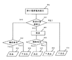
図10は本発明の冗長救済方法における検査フロー例を示す図である。本検査フローにおいて、201は静止電源電流測定、202は静止電源電流測定結果による検査対象回路が正常か異常かの判別、203は検査対象回路が異常であった場合に実施する冗長救済、204は検査対象回路が正常であった場合の製品A、205は検査対象回路が異常でかつ冗長救済を実施した製品Bである。製品Bは検査対象回路が異常なため冗長回路のみが使用可能であるが、製品Aは検査対象回路も冗長回路も正常なため両方の回路が使用可能である。このような冗長救済方法により、両方の回路が使用可能な製品Aと片方の回路のみが使用可能な製品Bを区別して製造することができる。 FIG. 10 is a diagram showing an example of an inspection flow in the redundancy repair method of the present invention. In this inspection flow, 201 is a quiescent power supply current measurement, 202 is a determination as to whether the inspection target circuit is normal or abnormal based on the quiescent power supply current measurement result, 203 is a redundant relief performed when the inspection target circuit is abnormal, and 204 is Products A and 205 when the circuit to be inspected is normal are products B in which the circuit to be inspected is abnormal and redundant relief has been performed. Since product B has an abnormal circuit to be inspected, only the redundant circuit can be used. However, since product A has both the circuit to be inspected and the redundant circuit normal, both circuits can be used. By such a redundant repair method, the product A that can use both circuits and the product B that can use only one circuit can be distinguished from each other.
図11は本発明の冗長救済方法における他の検査フロー例を示す図である。本検査フローにおいては、機能検査212を実施する前に、まず静止電源電流測定201を行い、冗長救済203を実施することにより、機能検査後の冗長救済工程を削除し、テスト時間の短縮、テストコスト削減を図ることができる。
FIG. 11 is a diagram showing another inspection flow example in the redundancy repair method of the present invention. In this test flow, before performing the
(実施の形態2)
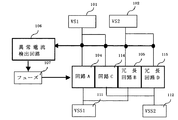
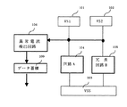
図2は本発明の実施の形態2に係る冗長救済方法を示す半導体集積回路装置の構成図である。本実施の形態は、実施の形態1の接地VSS103を個別の接地VSS1(111)とVSS2(112)に分割し、個別の電源101および102と組合せたものである。本実施の形態における他の構成要素は実施の形態1と同じであり、本実施の形態の冗長救済方法を実施した検査フローや半導体集積回路装置の組立に関する技術も実施の形態1と同じであるので、説明を省略する。このように構成することで、個別の電源を増加させることなく、検査対象回路A104とは異なる検査対象回路C114と冗長回路D115を追加することができ、冗長救済を自動的に行う回路を増やすことが可能となる。
(Embodiment 2)
FIG. 2 is a configuration diagram of a semiconductor integrated circuit device showing a redundancy repair method according to the second embodiment of the present invention. In the present embodiment, the
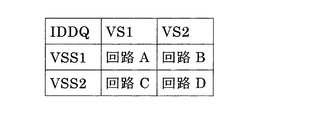
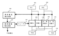
図3は図2の構成における個別の電源と個別の接地の組合せ方を示す図である。2つの電源VS1、VS2と2つの接地VSS1、VSS2を組合せることで、2つの検査対象回路A、検査対象回路Cと2つの冗長回路B、冗長回路Dを設けることができ、検査対象回路Aと検査対象回路Cの2つの回路の救済が可能になる。 FIG. 3 is a diagram showing a combination of individual power sources and individual grounds in the configuration of FIG. By combining the two power sources VS1 and VS2 and the two grounds VSS1 and VSS2, it is possible to provide two test target circuits A, a test target circuit C, two redundant circuits B, and a redundant circuit D. The test target circuit A And the circuit C to be inspected can be relieved.
図9は図2の構成における冗長回路105と冗長回路115を一つにした構成図である。図9において、110は異常電流検出回路106の測定結果を選別する異常個数検出回路である。本構成において、救済回路が1つで検査対象回路が2個以上不良となった場合は、不良フラグをたてて不良扱いにする。このように冗長回路を削減することでチップ面積を削減することができる。
FIG. 9 is a configuration diagram in which the
本発明の冗長救済方法は、半導体集積回路の加工技術の微細化に伴い、機能ファンクションだけでは救済しきれない半断線や半ショートの歩留りを向上させる検査に有効である。 The redundancy repair method of the present invention is effective for inspections that improve the yield of half-breaks and half-shorts that cannot be repaired only by functional functions as the processing technology of semiconductor integrated circuits is miniaturized.
101 第1の個別電源VS1
102 第2の個別電源VS2
103 共通接地VSS
104 検査対象回路A
105 冗長回路B
106 異常電流検出回路
107 ヒューズボックス
108 ヒューズ
109 データ蓄積回路
110 異常個数検出回路
111 第1の個別接地VSS1
112 第2の個別接地VSS2
114 検査対象回路C
115 冗長回路D
121 冗長救済実施の静止電源電流テストモード
122 テストモード時にオンになるスイッチ
123 規格電流
124 比較回路
125 レベルシフタ
126 選択回路
131 VS1用電源端子
132 VS2用電源端子
133 VSS接地端子
134 電流値出力端子
135 異常電流結果入力端子
101 First individual power supply VS1
102 Second individual power supply VS2
103 Common ground VSS
104 Circuit A to be inspected
105 Redundant circuit B
106 Abnormal
112 Second individual ground VSS2
114 Circuit C to be inspected
115 Redundant circuit D
121 Static power supply current test mode for performing
Claims (9)
Priority Applications (1)
| Application Number | Priority Date | Filing Date | Title |
|---|---|---|---|
| JP2006017842A JP2007201166A (en) | 2006-01-26 | 2006-01-26 | Redundant relief method for semiconductor integrated circuit device |
Applications Claiming Priority (1)
| Application Number | Priority Date | Filing Date | Title |
|---|---|---|---|
| JP2006017842A JP2007201166A (en) | 2006-01-26 | 2006-01-26 | Redundant relief method for semiconductor integrated circuit device |
Publications (1)
| Publication Number | Publication Date |
|---|---|
| JP2007201166A true JP2007201166A (en) | 2007-08-09 |
Family
ID=38455447
Family Applications (1)
| Application Number | Title | Priority Date | Filing Date |
|---|---|---|---|
| JP2006017842A Withdrawn JP2007201166A (en) | 2006-01-26 | 2006-01-26 | Redundant relief method for semiconductor integrated circuit device |
Country Status (1)
| Country | Link |
|---|---|
| JP (1) | JP2007201166A (en) |
Cited By (1)
| Publication number | Priority date | Publication date | Assignee | Title |
|---|---|---|---|---|
| CN115798343A (en) * | 2021-09-10 | 2023-03-14 | 乐金显示有限公司 | Display device |
-
2006
- 2006-01-26 JP JP2006017842A patent/JP2007201166A/en not_active Withdrawn
Cited By (1)
| Publication number | Priority date | Publication date | Assignee | Title |
|---|---|---|---|---|
| CN115798343A (en) * | 2021-09-10 | 2023-03-14 | 乐金显示有限公司 | Display device |
Similar Documents
| Publication | Publication Date | Title |
|---|---|---|
| US7877657B1 (en) | Look-ahead built-in self tests | |
| US20060125470A1 (en) | System and method for IDDQ measurement in system on a chip (SOC) design | |
| KR980010774A (en) | Semiconductor circuit systems, inspection methods for semiconductor integrated circuits and methods of generating the inspection series | |
| JP4481588B2 (en) | Semiconductor integrated circuit device | |
| JP2010004072A (en) | Semiconductor integrated circuit device and method for inspecting the same, semiconductor wafer, and burn-in inspection device | |
| US20060268485A1 (en) | Fuse cutting test circuit, fuse cutting test method, and semiconductor circuit | |
| JP5067266B2 (en) | Integrated circuit board with JTAG function | |
| JP2009092529A (en) | Semiconductor circuit and inspection method of the same | |
| JP2007201166A (en) | Redundant relief method for semiconductor integrated circuit device | |
| US7847574B2 (en) | Semiconductor device | |
| JP2011123725A (en) | Computer circuit and fault inspection method | |
| US7516375B2 (en) | Methods and systems for repairing an integrated circuit device | |
| JP2991994B2 (en) | Semiconductor circuit system, inspection method of semiconductor integrated circuit, and method of generating inspection sequence | |
| JP2006222200A (en) | Semiconductor chip | |
| KR100506667B1 (en) | Semiconductor integrated circuit | |
| US7622947B1 (en) | Redundant circuit presents connections on specified I/O ports | |
| JP3931189B2 (en) | Multi-chip package inspection method | |
| JPH0829502A (en) | Semiconductor chip on which testable logic and memory are loaded together | |
| JP5573638B2 (en) | Information processing apparatus and operating method thereof | |
| JP2014202634A (en) | Electric inspection method for bidirectional signal line of electric circuit | |
| JP2006284493A (en) | Semiconductor device and circuit test method for semiconductor device | |
| CN100492545C (en) | Memory bit line leak repair | |
| JPH09251797A (en) | Semiconductor memory device, repairing method thereof, and testing method thereof | |
| US20050073893A1 (en) | Memory bit line leakage repair | |
| JP2007225514A (en) | Semiconductor integrated circuit device and inspection method thereof |
Legal Events
| Date | Code | Title | Description |
|---|---|---|---|
| RD02 | Notification of acceptance of power of attorney |
Free format text: JAPANESE INTERMEDIATE CODE: A7422 Effective date: 20071113 |
|
| RD04 | Notification of resignation of power of attorney |
Free format text: JAPANESE INTERMEDIATE CODE: A7424 Effective date: 20071120 |
|
| A300 | Application deemed to be withdrawn because no request for examination was validly filed |
Free format text: JAPANESE INTERMEDIATE CODE: A300 Effective date: 20090407 |