JP2007200714A - Dye-sensitized solar cell and its manufacturing method - Google Patents
Dye-sensitized solar cell and its manufacturing method Download PDFInfo
- Publication number
- JP2007200714A JP2007200714A JP2006017939A JP2006017939A JP2007200714A JP 2007200714 A JP2007200714 A JP 2007200714A JP 2006017939 A JP2006017939 A JP 2006017939A JP 2006017939 A JP2006017939 A JP 2006017939A JP 2007200714 A JP2007200714 A JP 2007200714A
- Authority
- JP
- Japan
- Prior art keywords
- dye
- layer
- solar cell
- sensitized solar
- aqueous solution
- Prior art date
- Legal status (The legal status is an assumption and is not a legal conclusion. Google has not performed a legal analysis and makes no representation as to the accuracy of the status listed.)
- Pending
Links
Images

Classifications
-
- Y—GENERAL TAGGING OF NEW TECHNOLOGICAL DEVELOPMENTS; GENERAL TAGGING OF CROSS-SECTIONAL TECHNOLOGIES SPANNING OVER SEVERAL SECTIONS OF THE IPC; TECHNICAL SUBJECTS COVERED BY FORMER USPC CROSS-REFERENCE ART COLLECTIONS [XRACs] AND DIGESTS
- Y02—TECHNOLOGIES OR APPLICATIONS FOR MITIGATION OR ADAPTATION AGAINST CLIMATE CHANGE
- Y02E—REDUCTION OF GREENHOUSE GAS [GHG] EMISSIONS, RELATED TO ENERGY GENERATION, TRANSMISSION OR DISTRIBUTION
- Y02E10/00—Energy generation through renewable energy sources
- Y02E10/50—Photovoltaic [PV] energy
- Y02E10/542—Dye sensitized solar cells
-
- Y—GENERAL TAGGING OF NEW TECHNOLOGICAL DEVELOPMENTS; GENERAL TAGGING OF CROSS-SECTIONAL TECHNOLOGIES SPANNING OVER SEVERAL SECTIONS OF THE IPC; TECHNICAL SUBJECTS COVERED BY FORMER USPC CROSS-REFERENCE ART COLLECTIONS [XRACs] AND DIGESTS
- Y02—TECHNOLOGIES OR APPLICATIONS FOR MITIGATION OR ADAPTATION AGAINST CLIMATE CHANGE
- Y02P—CLIMATE CHANGE MITIGATION TECHNOLOGIES IN THE PRODUCTION OR PROCESSING OF GOODS
- Y02P70/00—Climate change mitigation technologies in the production process for final industrial or consumer products
- Y02P70/50—Manufacturing or production processes characterised by the final manufactured product
Abstract
Description
本発明は、色素増感型太陽電池及びその製造方法に関するものである。 The present invention relates to a dye-sensitized solar cell and a method for producing the same.
色素増感型太陽電池は、色素を吸着させた半導体電極と、この半導体電極に対向する対向電極と、これらの電極間に挟持された電解質とから構成されており、色素で吸収した光エネルギーを電気エネルギーに変換することによって発電するものである。このような色素増感型太陽電池は、原材料費が安価で安全性が高いことなどから実用化が期待されている。
色素増感型太陽電池で用いられる半導体電極は、一般に、透明基板上に形成された導電体層上に半導体微粒子の分散液を塗布・焼成して半導体層を形成した後、この半導体層に色素を吸着させることにより製造される。しかしながら、このような方法で製造された半導体電極では、個々の半導体微粒子の間に隙間が生じてしまう。そのため、この半導体電極を備えた色素増感型太陽電池では、該隙間を介して電解質と導電体層とが直接接触して漏れ電流を引き起こし、光電変換効率を低下させてしまう。
そこで、電解質と導電体層との直接接触を防ぐため、透明基板上に形成された導電体層上にスプレーパイロリシス法を用いて二酸化チタン層を形成させることにより、導電体層と半導体層との間に二酸化チタン層を配置する方法がある(例えば、非特許文献1参照)。また、透明基板上に形成された導電体層上にチタンアルコキシド溶液を塗布・焼成して逆電子注入防止層を形成させることにより、導電体層と半導体層との間に逆電子注入防止層を配置する方法がある(例えば、特許文献1参照)。
A dye-sensitized solar cell is composed of a semiconductor electrode on which a dye is adsorbed, a counter electrode facing the semiconductor electrode, and an electrolyte sandwiched between the electrodes, and absorbs light energy absorbed by the dye. It generates electricity by converting it into electrical energy. Such dye-sensitized solar cells are expected to be put to practical use because raw material costs are low and safety is high.
A semiconductor electrode used in a dye-sensitized solar cell generally has a semiconductor layer formed by coating and baking a dispersion of semiconductor fine particles on a conductor layer formed on a transparent substrate, and then the dye is applied to the semiconductor layer. It is manufactured by adsorbing. However, in the semiconductor electrode manufactured by such a method, a gap is generated between individual semiconductor fine particles. Therefore, in the dye-sensitized solar cell provided with this semiconductor electrode, the electrolyte and the conductor layer are in direct contact with each other through the gap to cause a leakage current, thereby reducing the photoelectric conversion efficiency.
Therefore, in order to prevent direct contact between the electrolyte and the conductor layer, the conductor layer and the semiconductor layer are formed by forming a titanium dioxide layer on the conductor layer formed on the transparent substrate using a spray pyrolysis method. There is a method of disposing a titanium dioxide layer between them (for example, see Non-Patent Document 1). In addition, a reverse electron injection prevention layer is formed between the conductor layer and the semiconductor layer by applying and baking a titanium alkoxide solution on the conductor layer formed on the transparent substrate to form a reverse electron injection prevention layer. There is a method of arranging (see, for example, Patent Document 1).
しかしながら、上記従来方法によって二酸化チタン層又は逆電子注入防止層を導電体層と半導体層との間に配置した色素増感型太陽電池では、導電体層と電解質との直接接触を防ぎ、漏れ電流を少なくして開放電流を向上させることができるものの、内部抵抗が増加して電流電圧曲線におけるフィルファクターが大きく低下してしまい、光電変換効率が低下してしまうという問題があった。
したがって、本発明は、上記のような問題を解決するためになされたものであり、漏れ電流及び内部抵抗が抑制された光電変換効率の高い色素増感型太陽電池及びその製造方法を得ることを目的とする。
However, in the dye-sensitized solar cell in which the titanium dioxide layer or the reverse electron injection preventing layer is disposed between the conductor layer and the semiconductor layer by the above-described conventional method, direct contact between the conductor layer and the electrolyte is prevented and leakage current is prevented. However, there is a problem that the internal resistance increases, the fill factor in the current-voltage curve is greatly reduced, and the photoelectric conversion efficiency is lowered.
Therefore, the present invention has been made to solve the above problems, and to obtain a dye-sensitized solar cell with high photoelectric conversion efficiency in which leakage current and internal resistance are suppressed, and a method for producing the same. Objective.
そこで、本発明者らは上記のような問題を解決すべく鋭意研究した結果、内部抵抗の増加が、導電体層と半導体層との間に配置される層の厚さに起因するという見地に基づき、特定の材料を用いて、導電体層と半導体層との間に薄くて緻密な漏れ電流抑制層を形成させることで、漏れ電流及び内部抵抗を抑制することができることに想到し、本発明を完成するに至った。
すなわち、本発明は、ペルオキソチタン酸系水溶液を、透明基板上に形成された導電体層上に塗布して乾燥させ、焼成することにより漏れ電流抑制層を形成した後、前記漏れ電流抑制層上に半導体層を形成し、次いで前記半導体層に色素を吸着させることにより半導体電極を調製する工程を含むことを特徴とする色素増感型太陽電池の製造方法である。
また、本発明は、上記方法によって製造される色素増感型太陽電池である。
Therefore, as a result of intensive studies to solve the above problems, the present inventors have found that the increase in internal resistance is caused by the thickness of the layer disposed between the conductor layer and the semiconductor layer. Based on this, it was conceived that the leakage current and the internal resistance can be suppressed by forming a thin and dense leakage current suppressing layer between the conductor layer and the semiconductor layer using a specific material. It came to complete.
That is, the present invention is to apply a peroxotitanic acid-based aqueous solution on a conductor layer formed on a transparent substrate, dry it, and fire it to form a leakage current suppression layer, and then on the leakage current suppression layer. A method for producing a dye-sensitized solar cell, comprising the steps of: forming a semiconductor layer, and then preparing a semiconductor electrode by adsorbing the dye to the semiconductor layer.
Moreover, this invention is a dye-sensitized solar cell manufactured by the said method.
本発明によれば、ペルオキソチタン酸系水溶液を用いて、アスペクト比の高い微粒子からなる薄くて緻密な漏れ電流抑制層を導電体層と半導体層との間に形成させることにより、漏れ電流及び内部抵抗が抑制された光電変換効率の高い色素増感型太陽電池を製造することができる。 According to the present invention, by using a peroxotitanic acid-based aqueous solution, a thin and dense leakage current suppression layer made of fine particles having a high aspect ratio is formed between the conductor layer and the semiconductor layer, whereby leakage current and internal It is possible to manufacture a dye-sensitized solar cell with high resistance and reduced photoelectric conversion efficiency.
以下に、図面を参照して本発明の実施の形態について説明する。
図1は、本発明の実施の形態における色素増感型太陽電池の断面模式図である。図1において、色素増感型太陽電池は、半導体電極7と、この半導体電極7に対向する対向電極6と、これらの電極間に挟持された電解質5とから構成されている。半導体電極7は、透明基板1と、この透明基板1上に形成された導電体層2と、この導電体層2上に形成された漏れ電流抑制層3と、この漏れ電流抑制層3上に形成され、色素が吸着された半導体層4とから構成されている。
Embodiments of the present invention will be described below with reference to the drawings.
FIG. 1 is a schematic cross-sectional view of a dye-sensitized solar cell according to an embodiment of the present invention. In FIG. 1, the dye-sensitized solar cell includes a
漏れ電流抑制層3は、ペルオキソチタン酸系水溶液を、透明基板1上に形成された導電体層2上に塗布して乾燥させ、焼成することにより形成させることができる。本実施の形態において、漏れ電流抑制層3を形成するために用いられるペルオキソチタン酸系水溶液としては、ペルオキソチタン酸水溶液及びペルオキソチタン酸改質アナターゼ型酸化チタン水系ゾルを挙げることができる。
ペルオキソチタン酸水溶液は、下記式の基本構造を有する二核錯体アニオンTi2O5(OH)x (2−x)−(x>2)や、そのポリアニオン((Ti2O5)q(OH)y (y−2q)−、(2<q/y))等を含んでいると考えられるものであり、低濃度の不純物イオンで安定化されていることを特徴としている。
The leakage
The peroxotitanic acid aqueous solution is composed of a binuclear complex anion Ti 2 O 5 (OH) x (2-x) − (x> 2) having a basic structure of the following formula and a polyanion ((Ti 2 O 5 ) q (OH). ) Y (y-2q) − , (2 <q / y)) and the like, and is characterized by being stabilized with a low concentration of impurity ions.

このようなペルオキソチタン酸水溶液としては、特に制限されず、公知の方法により製造されたものを用いることができる。例えば、まず、低濃度のTiCl4水溶液(0.1mol/dm3)に30重量%過剰のH2O2を加えて得られる溶液とNH4OHとを1:9の重量比で混合し、pHを10に調整することによって、沈殿物としてのペルオキソ水和物を得る。得られたペルオキソ水和物を蒸留水で洗浄し、不純物のNH4 +及びCl−をイオン交換樹脂によって取り除く。次いで、このペルオキソ水和物と、30重量%過剰のH2O2とを7℃で混合して反応させることによって、ペルオキソチタン酸水溶液(0.1mol/dm3)を製造することができる。このようにして製造されるペルオキソチタン酸水溶液には、0.014mol/dm3のNH4 +と0.0085mol/dm3のCl−が含まれている。
また、このようなペルオキソチタン酸水溶液として、PTA(鯤コーポレイション)等の市販製品を使用することも可能である。
Such an aqueous peroxotitanic acid solution is not particularly limited, and an aqueous solution prepared by a known method can be used. For example, first, a solution obtained by adding 30 wt% excess H 2 O 2 to a low concentration TiCl 4 aqueous solution (0.1 mol / dm 3 ) and NH 4 OH are mixed at a weight ratio of 1: 9, By adjusting the pH to 10, peroxohydrate as a precipitate is obtained. The resulting peroxohydrate is washed with distilled water, and impurities NH 4 + and Cl − are removed by an ion exchange resin. Next, an aqueous peroxotitanic acid solution (0.1 mol / dm 3 ) can be produced by mixing and reacting this peroxohydrate with an excess of 30% by weight of H 2 O 2 at 7 ° C. The peroxotitanic acid aqueous solution thus produced contains 0.014 mol / dm 3 NH 4 + and 0.0085 mol / dm 3 Cl − .
Moreover, as such a peroxotitanic acid aqueous solution, it is also possible to use commercial products, such as PTA (Tsubaki Corporation).
ペルオキソチタン酸改質アナターゼ型酸化チタン水系ゾルは、ペルオキソチタン酸水溶液中にアナターゼ型酸化チタンの結晶を含有するものである。このアナターゼ型酸化チタンの結晶は、扁平、紡錘状又は矢尻状等の形状を有し、数nm〜30nmの大きさである。
このようなペルオキソチタン酸改質アナターゼ型酸化チタン水系ゾルは、上記ペルオキソチタン酸水溶液を、65℃〜100℃で2〜40時間加熱することにより、ペルオキソチタン酸の一部又は全部を、アモルファス型酸化チタン、さらにはアナターゼ型結晶の前駆体とし、それを経てアナターゼ型酸化チタンに結晶化させることができる。この際、加熱温度の下限は、80℃以上が好ましく、90℃以上であることがより好ましく、また加熱温度の上限は、95℃以下が好ましい。さらに、加熱時間は、4〜15時間が好ましい。加熱温度が65℃未満であると、ペルオキソチタン酸の一部又は全部をアナターゼ型酸化チタンに速やかに結晶化させることができない傾向にあり、一方、100℃を超えると、副反応が生じたり、水等が揮発しすぎる傾向にあるので好ましくない。同様に、加熱温度が2時間未満であると、ペルオキソチタン酸の一部又は全部をアナターゼ型酸化チタンに十分に結晶化させることができない傾向にあり、一方、40時間を超えると、水等が揮発しすぎる傾向にあるので好ましくない。
また、このようペルオキソチタン酸改質アナターゼ型酸化チタン水系ゾルとして、TOsol、TPX(共に鯤コーポレイション)等の市販製品を使用することも可能である。
The peroxotitanate-modified anatase-type titanium oxide aqueous sol contains anatase-type titanium oxide crystals in a peroxotitanate aqueous solution. This anatase-type titanium oxide crystal has a flat shape, a spindle shape, an arrowhead shape, or the like, and has a size of several nm to 30 nm.
Such a peroxotitanic acid-modified anatase-type titanium oxide aqueous sol is obtained by heating the peroxotitanic acid aqueous solution at 65 ° C. to 100 ° C. for 2 to 40 hours, so that part or all of the peroxotitanic acid is converted into an amorphous type. It can be made into a precursor of titanium oxide and further anatase type crystal, and then crystallized into anatase type titanium oxide. In this case, the lower limit of the heating temperature is preferably 80 ° C. or higher, more preferably 90 ° C. or higher, and the upper limit of the heating temperature is preferably 95 ° C. or lower. Furthermore, the heating time is preferably 4 to 15 hours. When the heating temperature is less than 65 ° C., there is a tendency that part or all of peroxotitanic acid cannot be rapidly crystallized into anatase-type titanium oxide, while when it exceeds 100 ° C., side reactions occur, Since water etc. tend to volatilize too much, it is not preferable. Similarly, if the heating temperature is less than 2 hours, a part or all of peroxotitanic acid tends to be insufficiently crystallized in anatase-type titanium oxide. Since it tends to volatilize too much, it is not preferable.
Moreover, as such a peroxotitanate-modified anatase-type titanium oxide aqueous sol, commercially available products such as TOsol and TPX (both are Tsubaki Corporation) can also be used.
漏れ電流抑制層3を形成するために用いられるペルオキソチタン酸系水溶液は、固形分濃度が0.1〜3.0重量%であることが好ましく、0.5〜2.5重量%であることがより好ましい。固形分濃度が0.1重量%未満であると、薄すぎて漏れ電流抑制層3を形成させる際に何度も塗り重ねる必要があり、生産効率が悪く実用的でない傾向にあるので好ましくない。一方、固形分濃度が3.0重量%を超えると、該ペルオキソチタン酸系水溶液の貯蔵安定性を著しく損なうおそれがあり、また形成される漏れ電流抑制層3の透明性、硬度、密着性及び耐磨耗性が低下する傾向にあるので好ましくない。
なお、本実施の形態におけるペルオキソチタン酸系水溶液の固形分濃度とは、該水溶液の調製時に推定される、該水溶液に対する溶媒以外の成分の重量比率、又は該水溶液に対する乾燥後の固形分の重量比率のことを意味する。
The peroxotitanic acid aqueous solution used for forming the leakage current suppressing
The solid content concentration of the peroxotitanic acid aqueous solution in the present embodiment is the weight ratio of components other than the solvent to the aqueous solution, estimated at the time of preparing the aqueous solution, or the weight of the solid content after drying with respect to the aqueous solution. It means the ratio.
また、ペルオキソチタン酸系水溶液として、ペルオキソチタン酸水溶液及びペルオキソチタン酸改質アナターゼ型酸化チタン水系ゾルの混合物を用いて漏れ電流抑制層3を形成してもよい。
この混合物において、ペルオキソチタン酸水溶液とペルオキソチタン酸改質アナターゼ型酸化チタン水系ゾルとの配合割合は特に制限されることはない。ペルオキソチタン酸系水溶液の固形分濃度が0.1〜3.0重量%である場合には、0重量%を超え70重量%以下のペルオキソチタン酸水溶液と、30重量%以上100重量%未満のペルオキソチタン酸改質アナターゼ型酸化チタン水系ゾルとを混合することが好ましく、0重量%を超え50重量%以下のペルオキソチタン酸水溶液と、50重量%以上100重量%未満のペルオキソチタン酸改質アナターゼ型酸化チタン水系ゾルとを混合することがより好ましく、0重量%を超え30重量%以下のペルオキソチタン酸水溶液と、70重量%以上100重量%未満のペルオキソチタン酸改質アナターゼ型酸化チタン水系ゾルとを混合することが最も好ましい。ペルオキソチタン酸水溶液とペルオキソチタン酸改質アナターゼ型酸化チタン水系ゾルとの配合割合が上記範囲内であれば、より緻密な漏れ電流抑制層3が得られ、漏れ電流抑制効果を向上させることができる。
Further, the leakage
In this mixture, the mixing ratio of the peroxotitanate aqueous solution and the peroxotitanate-modified anatase-type titanium oxide aqueous sol is not particularly limited. When the solid content concentration of the peroxotitanic acid aqueous solution is 0.1 to 3.0% by weight, the peroxotitanic acid aqueous solution is more than 0% by weight and 70% by weight or less, and 30% by weight or more and less than 100% by weight. It is preferable to mix a peroxotitanate-modified anatase-type titanium oxide aqueous sol, and an aqueous peroxotitanate solution of more than 0% by weight and 50% by weight or less and a peroxotitanate-modified anatase of 50% by weight to less than 100% by weight It is more preferable to mix a water-type titanium oxide aqueous sol with a peroxotitanic acid aqueous solution of more than 0% by weight and 30% by weight or less and a peroxotitanic acid-modified anatase-type titanium oxide aqueous sol of 70% by weight to less than 100% by weight. And are most preferably mixed. If the blending ratio of the peroxotitanic acid aqueous solution and the peroxotitanate-modified anatase-type titanium oxide aqueous sol is within the above range, a denser leakage current suppressing
上記ペルオキソチタン酸系水溶液は、中性ないし弱塩基性を示すため、耐酸性のない金属等の材料にも適用可能である。また、上記ペルオキソチタン酸系水溶液は、長期にわたりゲル化しないので、長時間にわたる量産時にも安定的に供給することができ、安全性が非常に高く、取扱いが容易である。また、上記ペルオキソチタン酸系水溶液から得られる膜は、無定形のペルオキソチタン水和物Ti2O5(OH)2であるが、250℃以上に加熱することでアナターゼ型の二酸化チタンに結晶化させることができる。このアナターゼ型結晶は、ペルオキソチタン酸水溶液の基本構造であるペルオキソチタン二核錯体が平面的構造であるため、(101)面に強く配向するという特性を有する。また、上記ペルオキソチタン酸系水溶液から得られる膜中のペルオキソ基は、加熱や紫外線で分解され、膜の緻密化及び無定形TiO2への変化が徐々に起こるため、膜硬度が自ら向上していくという特性を示す。さらに、上記ペルオキソチタン酸系水溶液は、非常に平滑な膜を形成し易く、且つその膜は密着性に優れている。従って、上記ペルオキソチタン酸系水溶液から形成される漏れ電流抑制層3は、(101)面に配向し、薄くて緻密な密着性及び透明性等に優れたものとなる。
Since the peroxotitanic acid aqueous solution exhibits neutrality or weak basicity, it can be applied to materials such as metals having no acid resistance. Further, the peroxotitanic acid-based aqueous solution does not gel for a long period of time, so that it can be stably supplied even during mass production over a long period of time, is extremely safe and easy to handle. The film obtained from the peroxotitanic acid aqueous solution is amorphous peroxotitanium hydrate Ti 2 O 5 (OH) 2 , but is crystallized into anatase-type titanium dioxide by heating to 250 ° C. or higher. Can be made. This anatase-type crystal has a characteristic that the peroxotitanium dinuclear complex, which is the basic structure of the peroxotitanic acid aqueous solution, has a planar structure and is thus strongly oriented in the (101) plane. In addition, the peroxo group in the film obtained from the peroxotitanic acid-based aqueous solution is decomposed by heating and ultraviolet rays, and the film becomes denser and gradually changes to amorphous TiO 2 . The characteristic of going. Further, the peroxotitanic acid-based aqueous solution is easy to form a very smooth film, and the film is excellent in adhesion. Therefore, the leakage current suppressing
漏れ電流抑制層3を形成する際の上記ペルオキソチタン酸系水溶液の塗布方法としては、特に制限されることはなく、ローラ法、ディップ法、エアーナイフ法、ブレード法、ワイヤーバー法、スライドホッパ法、エクストルージョン法、カーテン法、スピン法、スプレー法及びスクリーン印刷等の各種印刷法等を用いて塗布すればよい。
乾燥方法としては、特に制限されることはなく、大気雰囲気下、5〜150℃で15〜60分間乾燥させればよい。
焼成方法としては、大気又は酸素雰囲気下、250〜550℃、好ましくは350〜500℃で10〜60分間焼成することが好ましい。焼成温度が250℃未満であると、アナターゼ型の二酸化チタンに結晶化させることができず、緻密な漏れ電流抑制層3が得られない傾向にあるので好ましくない。一方、550℃を超えると、ガラス等からなる透明基板1の耐熱温度を超える可能性があるので好ましくない。
The method for applying the peroxotitanic acid aqueous solution when forming the leakage current suppressing
The drying method is not particularly limited, and may be dried at 5 to 150 ° C. for 15 to 60 minutes in an air atmosphere.
As a baking method, it is preferable to bake for 10 to 60 minutes at 250 to 550 ° C., preferably 350 to 500 ° C. in an air or oxygen atmosphere. If the firing temperature is less than 250 ° C., it cannot be crystallized into anatase-type titanium dioxide, and the dense leakage current suppressing
このようにして得られる漏れ電流抑制層3の厚さは、5〜500nmであることが好ましく、10〜250nmであることがより好ましい。5nm未満では、導電体層2と電解質5との直接接触の遮蔽効果が十分に得られず、漏れ電流抑制効果が低下する傾向にあるので好ましくない。また、500nmを超えると、内部抵抗の増加により、光電変換効率の向上に対する寄与が小さくなる傾向にあるので好ましくない。
The thickness of the leakage current suppressing
透明基板1としては、絶縁性及び透明性を有するものであれば特に制限されることはなく、ガラスや、ポリメチルメタクリレート、ポリカーボネート、ポリスチレン、ポリエチレンサルファイド、ポリエーテルスルホン、ポリオレフィン、ポリエチレンテレフタレート、ポリエチレンナフタレート、トリアセチルセルロース等のプラスチックを用いることができる。これらの中でも、太陽電池を使用する環境及び寿命の観点から、耐光性及び耐熱性を有するガラスを用いることがより好ましい。
また、入射光を有効に取り入れるために、導電体層2が形成されていない側の表面に反射防止層を設けてもよい。反射防止層の形成方法としては、特に制限されることはなく、ディッピング法やスパッタ法を用いて金属酸化物を形成する方法、エッチングにより表面に凹凸を形成する方法、又は反射防止フィルムを貼り付ける方法によって形成すればよい。
The transparent substrate 1 is not particularly limited as long as it has insulating properties and transparency. Glass, polymethyl methacrylate, polycarbonate, polystyrene, polyethylene sulfide, polyethersulfone, polyolefin, polyethylene terephthalate, polyethylene naphthalate. Plastics such as phthalate and triacetyl cellulose can be used. Among these, it is more preferable to use a glass having light resistance and heat resistance from the viewpoint of the environment in which the solar cell is used and the lifetime.
In order to effectively take in incident light, an antireflection layer may be provided on the surface on which the conductor layer 2 is not formed. The method of forming the antireflection layer is not particularly limited, and a method of forming a metal oxide using a dipping method or a sputtering method, a method of forming irregularities on the surface by etching, or an antireflection film is attached. It may be formed by a method.
導電体層2は、透明基板1上に形成される。この導電体層2に用いられる材料としては、導電性を有し、且つ可視光領域の吸収が少なく、実質的に透明であるものであれば特に制限されることはなく、一般的な金属や、導電性酸化物として知られている、酸化すず、酸化タンタル、酸化タングステン、チタン酸ストロンチウム、酸化コバルト、酸化ニッケル、酸化ルテニウム、酸化亜鉛及び酸化インジウム等の金属酸化物、又はこれらの固溶体若しくはドーピング処理体を用いることができる。ここで、実質的に透明とは、光(400〜900nmの可視光域)の透過率が10%以上であることを意味し、50%以上の透過率を有するものがより好ましく、70%以上の透過率を有するものが特に好ましい。
透明電極1上に導電体層2を形成する方法としては、特に制限されることはなく、真空蒸着法、反応性蒸着法、イオンビームアシスト蒸着法、スパッタリング法、イオンプレーティング法、プラズマCVD法及びゾル−ゲル法等を用いて行うことができる。
The conductor layer 2 is formed on the transparent substrate 1. The material used for the conductor layer 2 is not particularly limited as long as it has conductivity, has little absorption in the visible light region, and is substantially transparent. Known as conductive oxides, metal oxides such as tin oxide, tantalum oxide, tungsten oxide, strontium titanate, cobalt oxide, nickel oxide, ruthenium oxide, zinc oxide and indium oxide, or their solid solutions or doping A treatment body can be used. Here, “substantially transparent” means that the transmittance of light (visible light range of 400 to 900 nm) is 10% or more, more preferably 50% or more, more preferably 70% or more. Particularly preferred are those having a transmittance of
The method for forming the conductor layer 2 on the transparent electrode 1 is not particularly limited, and is a vacuum deposition method, a reactive deposition method, an ion beam assisted deposition method, a sputtering method, an ion plating method, a plasma CVD method. And a sol-gel method or the like.
半導体層4は、漏れ電流抑制層3上に形成される。この半導体層4は、ラフネスファクター(投影面積に対する実際の表面積の割合)が20倍以上、好ましくは500倍以上であることが必要である。このように表面粗さの大きな表面を有する半導体層4を形成すれば、単位面積当たりの表面積が大きくなり、吸着色素量が増加するので、光の吸収量を十分に増やすことができる。そのため、半導体層4は、粒径が5〜500nm程度の半導体粒子が積層融着したものであることが好ましい。このような半導体層4に用いられる材料としては、酸化チタン、酸化亜鉛、酸化タングステン、酸化ニオブ、酸化錫、酸化バナジウム、酸化インジウム、酸化タンタル、酸化ジルコニウム、酸化モリブデン、酸化マンガン、チタン酸バリウム、チタン酸ストロンチウム、チタン酸カルシウム、チタン酸マグネシウム、ニオブ酸ストロンチウム、炭化ケイ素及びGaP等の公知の半導体を、一種以上混合して用いることができる。これらの中でも、安定性及び安全性の観点から酸化チタンが好ましい。
また、上記酸化チタンは、アナターゼ型酸化チタン、ルチル型酸化チタン、無定形酸化チタン、メタ酸化チタン及びオルソ酸化チタン等の種々の酸化チタン、水酸化チタン、並びに含酸化チタン等であってよい。これらの中でも、光電変換効率の観点から、アナターゼ含有率が高いものが好ましく、80%以上であることがさらに好ましい。
The semiconductor layer 4 is formed on the leakage
The titanium oxide may be various titanium oxides such as anatase type titanium oxide, rutile type titanium oxide, amorphous titanium oxide, meta titanium oxide and ortho titanium oxide, titanium hydroxide, and titanium oxide. Among these, those having a high anatase content are preferable from the viewpoint of photoelectric conversion efficiency, and more preferably 80% or more.
半導体層4の厚さは、用途により異なり、透明性が要求されるならば薄くすればよく、高い光電変換効率が要求されるならば厚くすればよい。具体的には、半導体層4の厚さは、0.5〜50μmであることが好ましく、5〜30μmであることがより好ましい。半導体層4の厚さが0.5μm未満であると、入射光を吸収するのに十分な表面積が得られず、所望の光電変換効率が得られないおそれがあるので好ましくない。一方、半導体層4の厚さが50μmを超えると、光の吸収に寄与しない部分が増えて内部抵抗が増加し、所望の光電変換効率が得られないおそれがあるので好ましくない。 The thickness of the semiconductor layer 4 varies depending on the application, and may be reduced if transparency is required, and may be increased if high photoelectric conversion efficiency is required. Specifically, the thickness of the semiconductor layer 4 is preferably 0.5 to 50 μm, and more preferably 5 to 30 μm. If the thickness of the semiconductor layer 4 is less than 0.5 μm, a surface area sufficient to absorb incident light cannot be obtained, and the desired photoelectric conversion efficiency may not be obtained. On the other hand, if the thickness of the semiconductor layer 4 exceeds 50 μm, the portion that does not contribute to light absorption increases, the internal resistance increases, and the desired photoelectric conversion efficiency may not be obtained.
漏れ電流抑制層3上に半導体層4を形成する方法としては、特に制限されることはなく公知の方法を用いることがでる。具体的には、金属と炭素若しくは有機化合物とを、又は金属酸化物若しくは金属亜酸化物等と有機化合物とを真空中で同時に蒸着し共蒸着薄膜を酸化処理する方法、スパッタリング法等のようなドライプロセスや、ゾル−ゲル法、化学的な手法により作製された半導体微粒子の分散液を塗布する方法、半導体微粒子ペーストを塗布焼成する方法等のようなウエットプロセスを用いることができる。量産化、液物性や支持体の融通性を考えた場合、ウエットプロセスを用いた方が比較的有利である。ウエットプロセスに用いられる方法としては、塗布法、印刷法、スプレー法が代表的である。
The method for forming the semiconductor layer 4 on the leakage current suppressing
半導体微粒子の分散液を作製する方法としては、前述のゾル-ゲル法の他、乳鉢ですり潰す方法、ミルを使って粉砕しながら分散する方法、又は半導体を合成する際に溶媒中で微粒子として析出させそのまま使用する方法等が挙げられる。分散媒としては、水又は各種の有機溶媒(例えば、メタノール、エタノール、イソプロピルアルコール、ジクロロメタン、アセトン、アセトニトリル、酢酸エチル等)が挙げられる。分散の際、必要に応じてポリマー、界面活性剤、酸又はキレート剤等を分散助剤として用いてもよい。
半導体微粒子ペーストの作製法としては、半導体微粒子又は半導体微粒子の分散液に溶剤、増粘剤、酸、アルカリ等を添加して作製する。
塗布方法としては、ローラ法、ディップ法、エアーナイフ法、ブレード法、ワイヤーバー法、スライドホッパ法、エクストルージョン法、カーテン法、スピン法、スプレー法やスクリーン印刷等の各種印刷法等を用いることができる。
In addition to the sol-gel method described above, a method of preparing a dispersion of semiconductor fine particles is a method of grinding in a mortar, a method of dispersing while pulverizing using a mill, or a fine particle in a solvent when synthesizing a semiconductor. The method of depositing and using as it is is mentioned. Examples of the dispersion medium include water or various organic solvents (for example, methanol, ethanol, isopropyl alcohol, dichloromethane, acetone, acetonitrile, ethyl acetate, and the like). At the time of dispersion, a polymer, a surfactant, an acid, a chelating agent, or the like may be used as a dispersion aid as necessary.
The semiconductor fine particle paste is produced by adding a semiconductor fine particle or a dispersion of semiconductor fine particles to a solvent, a thickener, an acid, an alkali, or the like.
As a coating method, use various printing methods such as a roller method, a dip method, an air knife method, a blade method, a wire bar method, a slide hopper method, an extrusion method, a curtain method, a spin method, a spray method and a screen printing. Can do.
半導体層4は、ウエットプロセスを用いて形成された膜を焼成することにより得ることができる。この場合の焼成温度は、400〜550℃であることが好ましく、450〜500℃であることがより好ましい。焼成温度が400℃未満であると、半導体微粒子間の融着が少なくなり、発生した電子の集電効率が低下してしまう傾向にあるので好ましくない。一方、焼成温度が550℃を超えるとガラス等からなる透明基板1の耐熱温度を超える可能性があるので好ましくない。
また、焼成処理後、半導体粒子の表面積を増大させたり、半導体粒子近傍の純度を高め、色素から半導体粒子への電子注入効率を高めるなどの目的で、例えば、四塩化チタン水溶液を用いた化学メッキや、三塩化チタン水溶液を用いた電気化学的メッキ処理を行い、酸化チタン薄層を塗設してもよい。
The semiconductor layer 4 can be obtained by baking a film formed using a wet process. In this case, the firing temperature is preferably 400 to 550 ° C, and more preferably 450 to 500 ° C. When the firing temperature is less than 400 ° C., fusion between the semiconductor fine particles is reduced, and the current collection efficiency of the generated electrons tends to decrease, which is not preferable. On the other hand, if the firing temperature exceeds 550 ° C., it may exceed the heat resistance temperature of the transparent substrate 1 made of glass or the like, which is not preferable.
In addition, for example, chemical plating using an aqueous solution of titanium tetrachloride for the purpose of increasing the surface area of the semiconductor particles after firing, increasing the purity in the vicinity of the semiconductor particles, and increasing the efficiency of electron injection from the dye to the semiconductor particles. Alternatively, an electrochemical plating process using a titanium trichloride aqueous solution may be performed to coat a thin titanium oxide layer.
半導体層4に吸着させる色素としては、光を吸収するものであれば、特に制限されることなく用いることができる。このような色素としては、具体的には、ルテニウム、オスミウム、鉄又は亜鉛を1原子以上含有する金属錯体塩、無金属フタロシアニン、ポルフィリン,ジチオラート錯体,アセチルアセトナート錯体等の、いわゆる金属キレート錯体、NK1194、NK3422(日本感光色素研究所製)等のシアニン系色素、NK2426、NK2501(日本感光色素研究所製)等のメロシアニン系色素、ローズベンガル、ローダミンB等のキサンテン系色素、マラカイトグリーン、クリスタルバイオレット等のトリフェニルメタン系色素、銅フタロシアニン又はチタニルフタロシアニン等の金属フタロシアニン、クロロフィル、ヘミン、又はシアニジン色素、及びオキサジアゾール誘導体、ベンゾチアゾール誘導体、クマリン誘導体、スチルベン誘導体、芳香環を有する有機化合物等が挙げられる。これらの色素は、吸光係数が大きく且つ繰り返しの酸化還元に対して安定であることが好ましい。また、色素は低分子化合物であってもよいし、また繰り返し単位を有する高分子であってもよい。さらに、J会合体等の会合体を形成していても良い。中でも分光増感の効果や耐久性に優れている金属錯体、有機色素のJ会合体や顔料色素が好ましい。
また、上記色素は、半導体電極に化学的に吸着し得ることが好ましく、カルボキシル基、スルホン酸基、リン酸基、アミド基、アミノ基、カルボニル基、ホスフィン基等の官能基を有することが好ましい。また、このような官能基は色素分子中に複数個ある方が好ましい。
As a pigment | dye adsorb | sucked to the semiconductor layer 4, if it absorbs light, it can be used without a restriction | limiting in particular. Specific examples of such dyes include so-called metal chelate complexes such as metal complex salts containing at least one atom of ruthenium, osmium, iron or zinc, metal-free phthalocyanines, porphyrins, dithiolate complexes, and acetylacetonate complexes. Cyanine dyes such as NK1194 and NK3422 (manufactured by Nippon Photosensitivity Laboratories), merocyanine dyes such as NK2426 and NK2501 (manufactured by Nippon Photosensitivity Laboratories), xanthene dyes such as rose bengal and rhodamine B, malachite green, crystal violet Triphenylmethane dyes such as copper phthalocyanine or copper phthalocyanine or titanyl phthalocyanine, chlorophyll, hemin, or cyanidin dyes, and oxadiazole derivatives, benzothiazole derivatives, coumarin derivatives, stilbene derivatives Body, and organic compounds having an aromatic ring. These dyes preferably have a large extinction coefficient and are stable against repeated redox. The dye may be a low molecular compound or a polymer having a repeating unit. Further, an aggregate such as a J aggregate may be formed. Of these, metal complexes having excellent spectral sensitization effects and durability, J-aggregates of organic dyes, and pigment dyes are preferable.
The dye is preferably capable of being chemically adsorbed to the semiconductor electrode, and preferably has a functional group such as a carboxyl group, a sulfonic acid group, a phosphoric acid group, an amide group, an amino group, a carbonyl group, or a phosphine group. . Further, it is preferable that there are a plurality of such functional groups in the dye molecule.
本実施の形態における色素の半導体層4への吸着は、溶媒に色素を溶解した色素溶液を調製した後、その色素溶液に半導体層4を浸漬し、色素が吸着するのに十分な時間経過した後に、半導体層4を色素溶液より引き上げ、洗浄、乾燥することにより行うことができる。必要に応じて半導体層4を色素溶液に浸漬する際に、加熱してもよいし、色素溶液を酸性又は塩基性にしてもよい。
色素を溶解する溶媒としては、色素の溶解性に応じて適宜選択できる。例えば、水、アルコール類(メタノール、エタノール、t−ブタノール、ベンジルアルコール等)、ニトリル類(アセトニトリル、プロピオニトリル、3−メトキシプロピオニトリル等)、ニトロメタン、ハロゲン化炭化水素(ジクロロメタン、ジクロロエタン、クロロホルム、クロロベンゼン等)、エーテル類(ジエチルエーテル、テトラヒドロフラン等)、ジメチルスルホキシド、アミド類(N,N−ジメチルホルムアミド、N,N−ジメチルアセタミド等)、N−メチルピロリドン、1,3−ジメチルイミダゾリジノン、3−メチルオキサゾリジノン、エステル類(酢酸エチル、酢酸ブチル等)、炭酸エステル類(炭酸ジエチル、炭酸エチレン、炭酸プロピレン等)、ケトン類(アセトン、2−ブタノン、シクロヘキサノン等)、炭化水素(ヘキサン、石油エーテル、ベンゼン、トルエン等)やこれらの混合溶媒が挙げられる。
In the present embodiment, the dye is adsorbed onto the semiconductor layer 4 by preparing a dye solution in which the dye is dissolved in a solvent, and then immersing the semiconductor layer 4 in the dye solution, and a sufficient time has elapsed for the dye to adsorb. Later, the semiconductor layer 4 can be lifted from the dye solution, washed and dried. If necessary, the semiconductor layer 4 may be heated when immersed in the dye solution, or the dye solution may be acidic or basic.
The solvent for dissolving the dye can be appropriately selected according to the solubility of the dye. For example, water, alcohols (methanol, ethanol, t-butanol, benzyl alcohol, etc.), nitriles (acetonitrile, propionitrile, 3-methoxypropionitrile, etc.), nitromethane, halogenated hydrocarbons (dichloromethane, dichloroethane, chloroform) , Chlorobenzene, etc.), ethers (diethyl ether, tetrahydrofuran, etc.), dimethyl sulfoxide, amides (N, N-dimethylformamide, N, N-dimethylacetamide, etc.), N-methylpyrrolidone, 1,3-dimethylimidazo Lidinone, 3-methyloxazolidinone, esters (ethyl acetate, butyl acetate, etc.), carbonate esters (diethyl carbonate, ethylene carbonate, propylene carbonate, etc.), ketones (acetone, 2-butanone, cyclohexanone, etc.), carbonization Arsenide (hexane, petroleum ether, benzene, toluene, etc.) or mixed solvents thereof.
本実施の形態における電解質5としては、イオン輸送材料として、酸化還元対のイオンが溶解した溶液、酸化還元対の溶液をポリマーマトリクスのゲルに含浸した、いわゆるゲル電解質、酸化還元対イオンを含有する溶融塩電解質、さらには固体電解質が挙げられる。
電解質5に電解質溶液を使用する場合、電解質溶液は、電解質、溶媒及びその他の添加物から構成されることが好ましく、色素増感型太陽電池の電解質に一般に用いられる酸化還元剤を任意に用いることができる。本実施の形態における電解質5は、I2とヨウ化物との組み合わせ(ヨウ化物としては、LiI、NaI、KI、CsI、CaI2等の金属ヨウ化物、又はテトラアルキルアンモニウムヨーダイド、ピリジニウムヨーダイド、イミダゾリウムヨーダイド等の第4級アンモニウム化合物のヨウ素塩等)、Br2と臭化物との組み合わせ(臭化物としては、LiBr、NaBr、KBr、CsBr、CaBr2等の金属臭化物、又はテトラアルキルアンモニウムブロマイド、ピリジニウムブロマイド等の第4級アンモニウム化合物の臭素塩等)のほか、フェロシアン酸塩−フェリシアン酸塩やフェロセン−フェリシニウムイオン等の金属錯体、ポリ硫化ナトリウム、アルキルチオール−アルキルジスルフィド等のイオウ化合物、ビオローゲン色素、ヒドロキノン−キノン等を用いることができる。さらに、未結合電子を運搬するキノン錯体、テトラシアノキノンジメタン(TCNQ)錯体、ジシアノキノンジイミン錯体等の遷移金属錯体を使用することもできる。上述した電解質5は、混合して用いてもよい。この中でもI2とLiIやピリジニウムヨーダイド、イミダゾリウムヨーダイド等の第4級アンモニウム化合物のヨウ素塩を組み合わせた電解質等がより好ましい。
The
When an electrolyte solution is used for the
電解質溶液における電解質5の濃度は、0.1〜15Mであることが好ましく、0.2M〜10Mであることがより好ましい。電解質5の濃度が0.1M未満であると、電導度が低下する傾向にあるので好ましくない。一方、電解質5の濃度が15Mを超えると、溶液の粘度が増加して電導度が低下したり、又は温度の変動によって固形分が析出しまう傾向にあるので好ましくない。
また、電解質5にヨウ素を添加する場合、ヨウ素の添加濃度は0.01M〜5.0Mであることがより好ましい。ヨウ素の添加濃度が0.01M未満であると、電導度が低下する傾向にあるので好ましくない。一方、ヨウ素の添加濃度が5.0Mを超えると溶液の粘度が増加して電導度が低下したり、又は温度の変動によって固形分が析出しまう傾向にあるので好ましくない。
The concentration of the
Moreover, when adding an iodine to the
電解質溶液の溶剤としては、半導体電極に担持した色素が溶解しない有機溶剤であり、電気化学的に安定であり、電気化学的反応によるガスの発生等がないものが好ましい。このような溶剤の例としては、アセトニトリル、メトキシプロピオニトリル、メトキシアセトニトリル、炭酸プロピレン、炭酸エチレン及びメチルピロリドン、エチルアセテート又はテトラヒドロフラン、水、アルコール及びこれらの混合物等を挙げることができるが、これらに限定されるものではない。
電解質溶液の溶剤又は電解質として、溶融塩を使用することもできる。溶融塩は、光電変換効率と耐久性との両立という観点からより好ましい。溶融塩電解質の例としては、例えば、国際公開第95/18456号パンフレット、特開平8−259543号公報、電気化学第65巻第11号第923頁(1997年)等に記載されているピリジニウム塩、イミダゾリウム塩、トリアゾリウム塩等の既知のヨウ素塩等を用いることができる。
The solvent of the electrolyte solution is preferably an organic solvent that does not dissolve the dye supported on the semiconductor electrode, is electrochemically stable, and does not generate gas due to an electrochemical reaction. Examples of such solvents include acetonitrile, methoxypropionitrile, methoxyacetonitrile, propylene carbonate, ethylene carbonate and methyl pyrrolidone, ethyl acetate or tetrahydrofuran, water, alcohol and mixtures thereof. It is not limited.
A molten salt can also be used as the solvent or electrolyte of the electrolyte solution. Molten salt is more preferable from the viewpoint of achieving both photoelectric conversion efficiency and durability. Examples of the molten salt electrolyte include, for example, pyridinium salts described in International Publication No. 95/18456, JP-A-8-259543, Electrochemical Vol. 65, No. 11, 923 (1997), etc. Known iodine salts such as imidazolium salts and triazolium salts can be used.
本実施の形態においては、電解質5をゲル化させて使用することもできる。ゲル化の手法として、ポリマー添加、オイルゲル化剤添加、多官能モノマー類を含む重合、架橋反応等の手法によりポリマー添加する方法、ナノ微粒子を添加する方法等がある。架橋反応等によりゲル化させる場合は、ポリアクリロニトリル、ポリフッ化ビニリデンを使用することができる。オイルゲル化剤添加によりゲル化させる場合は、分子構造中にアミド構造を有する化合物を使用することが好ましい。
ゲル電解質を多官能モノマー類の重合によって形成する場合、多官能モノマー類、重合開始剤、電解質、溶媒からなる溶液から、色素を吸着させた半導体層4上にゾル状の電解質層を形成し、その後ラジカル重合することによってゲル化させる方法が好ましい。
In the present embodiment, the
When the gel electrolyte is formed by polymerization of polyfunctional monomers, a sol-like electrolyte layer is formed on the semiconductor layer 4 on which the dye is adsorbed from a solution composed of polyfunctional monomers, a polymerization initiator, an electrolyte, and a solvent. The method of making it gelatinize by radical polymerization after that is preferable.
本実施の形態においては、電解質5の代わりに有機若しくは無機、又はこの両者を組み合わせた電荷輸送材料を使用することができる。本実施の形態において適用可能な有機正孔輸送材料としては、トリフェニルアミン、ジフェニルアミン、フェニレンジアミン等の芳香族アミン化合物、ナフタレン、アントラセン、ビレン等の縮合多環炭化水素、アゾベンゼン等のアゾ化合物、スチルベン等の芳香環をエチレン結合やアセチレン結合で連結した構造を有する化合物、アミノ基で置換されたヘテロ芳香環化合物、ポルフィリン類、フタロシアン類、α−オクチルチオフェン、α,ω−ジヘキシル−α−オクチルチオフェン、ヘキサドデシルドデシチオフェン等のオリゴチオフェン化合物、ポリピロール、ポリアセチレン及びその誘導体、ポリ(p−フェニレン)及びその誘導体、ポリ(p−フェニレンビニレン)及びその誘導体、ポリチエニレンビニレン及びその誘導体、ポリチオフェン及びその誘導体、ポリアニリン及びその誘導体、ポリトルイジン及びその誘導体等の導電性高分子を使用することができる。電子輸送材料としては、キノン類、テトラシアノキノジメタン類、ジシアノキノンジイミン類、テトラシアノエチレン、ビオローゲン類、ジチオール金属錯体等が挙げられる。また、有機正孔(ホール)輸送材料には、ドーパントレベルをコントロールするために、トリス(4−ブロモフェニル)アミニウムヘキサクロロアンチモネートのようなカチオンラジカルを含有する化合物を添加したり、酸化物半導体表面のポテンシャル制御(空間電荷層の補償)を行うためにLi[(CF3SO2)2N]のような塩を添加しても構わない。その他、無機材料として、CuI、AgI、TiI及びその他の金属ヨウ化物、CuBr、CuSCN等を用いることができる。
また、性能改善のために、J.Am.Ceram.Soc.,80(12)3157−3171(1997)に記載されているようなter−ブチルピリジンや、2−ピコリン、2,6−ルチジン等の塩基性化合物を添加することもできる。塩基性化合物を添加する場合の好ましい濃度範囲は、0.05M〜2Mである。
In the present embodiment, instead of the
In order to improve performance, J. Org. Am. Ceram. Soc. , 80 (12) 3157-3171 (1997), and basic compounds such as ter-butylpyridine, 2-picoline, and 2,6-lutidine can also be added. A preferable concentration range when adding the basic compound is 0.05M to 2M.
本実施の形態における対向電極6としては、特に制限されることはなく、透明基板と導電体層とから構成されるものを用いることができる。対向電極6における透明基板及び導電体層としては、上記半導体電極7で用いた透明基板1及び導電体層2と同様のものを使用することができる。その他に、導電体層としては、触媒活性の高い材料を用いることも可能である。ここで、触媒活性の高い材料とは、酸化還元反応に対する触媒作用を有し、且つ電気化学的に安定な材料を意味する。触媒活性の高い材料の例としては、白金、パラジウム、ルテニウム、ニッケル、ロジウム、金又は白金等に、モリブデン、ルテニウム、スズ、鉄又はタングステンの少なくとも1つを添加した多元系触媒、又は酸化スズ、酸化ガリウム、酸化モリブデン等の金属酸化物及びこれらの混合材料、カーボン材料、ナノカーボン材料、白金等の触媒活性材料を担持したカーボン材料やナノカーボン材料、PEDOT−TsO等のポリチオフェン誘導体等の導電性高分子材料、高分子錯体触媒等が挙げられる。この中でも、電解質5に侵されにくく、且つ触媒活性が高い点で、白金、カーボン材料、及び触媒を担持したナノカーボン材料等が好ましい。
As the counter electrode 6 in this Embodiment, it does not restrict | limit in particular, What is comprised from a transparent substrate and a conductor layer can be used. As the transparent substrate and the conductor layer in the counter electrode 6, the same substrates as the transparent substrate 1 and the conductor layer 2 used in the
また、対向電極6の抵抗を下げるために、対向電極6に集電極を形成してもよい。集電極の材質としては、アルミニウム、金、銀、銅、白金、ニッケル、タングステン等の金属が好ましい。中でも導電性の観点から、金、銀、銅、ニッケル及びタングステンがより好ましい。この集電極は、公知の方法によって形成することができるが、蒸着法、スパッタリング法及びメッキ法等によって透明基板上に格子状等の集電極を形成した後、この集電極上に導電体層を形成することが好ましい。或いは、透明基板上に導電体層を形成した後、この導電体層上に格子状等の集電極を形成することも可能である。さらに、集電極と電解質5との直接接触を防ぎ、集電極の腐食を防止する観点から、封止材や、金属酸化物等の腐食防止層を集電極上に形成することも可能である。
In addition, a collector electrode may be formed on the counter electrode 6 in order to reduce the resistance of the counter electrode 6. As the material for the collector electrode, metals such as aluminum, gold, silver, copper, platinum, nickel, tungsten and the like are preferable. Among these, gold, silver, copper, nickel and tungsten are more preferable from the viewpoint of conductivity. This collector electrode can be formed by a known method, but after forming a grid-like collector electrode on a transparent substrate by vapor deposition, sputtering, plating, etc., a conductor layer is formed on this collector electrode. It is preferable to form. Alternatively, after forming a conductor layer on the transparent substrate, it is also possible to form a grid-like collector electrode on the conductor layer. Further, from the viewpoint of preventing direct contact between the collector electrode and the
半導体電極7、電解質5及び対向電極6からなる色素増感型太陽電池の作製は、特に制限されることはなく、公知の方法を用いればよい。具体的には、半導体電極7と対向電極6とを貼り合わせた後、その間隙に液状の電解質5を注入し封止する方法、半導体電極7の上に、穴を開けた対向電極6を貼り合わせて封止材によって封止を行った後、対向電極6の穴から電解質5を注入し注入口を封止する方法、半導体電極7上に直接電解質5を付与した後、対向電極6を貼り合わせる方法等を用いることができる。
また、電解質5を注入する際に、浸漬等による毛管現象を利用する常圧プロセスと、常圧より低い圧力にして電極間や多孔性膜中の気相を液相に置換する真空プロセスとを利用することができる。
The production of the dye-sensitized solar cell including the
In addition, when injecting the
電解質溶液のほかに、有機電荷輸送材料の溶液やゲル電解質を用いる場合には、半導体層4の形成方法や、半導体層4に色素を吸着させる方法と同様に、浸漬法、ローラ法、ディップ法、エアーナイフ法、エクストルージョン法、スライドホッパ法、ワーヤーバー法、スピン法、スプレー法、キャスト法、各種印刷法等を用いることができる。
固体電解質や固体の正孔(ホール)輸送材料を用いる場合には、真空蒸着法やCVD法等のドライ成膜処理、メッキ法や電解重合法等のウエット処理によって電解質の層を対向電極6上に形成した後、半導体電極7と貼り合わせることもできる。
半導体電極7と対向電極6との間に、フィルムシート、テープ状フィルムシート、多孔質シート、又は有機化合物若しくは無機化合物の微粒子等のスペーサーを挟み、半導体電極7と対向電極6との間に所望の距離を設けることもできる。
さらに、色素増感型太陽電池の作製にあたっては、半導体電極7と対向電極6との間の隙間を封止材によって封止することが好ましい。
封止材としては、特に制限されることはないが、耐光性、絶縁性及び防湿性を有する材料が好ましく、例えば、アイオノマー樹脂、エポキシ樹脂、紫外線硬化樹脂、アクリル系接着剤、エチレンビニルアセテート(EVA)、シリコンゴム、セラミック等の各種熱融着フィルム等を用いることができる。
When an organic charge transport material solution or gel electrolyte is used in addition to the electrolyte solution, the dipping method, the roller method, the dipping method, as in the method for forming the semiconductor layer 4 and the method for adsorbing the dye to the semiconductor layer 4 , Air knife method, extrusion method, slide hopper method, wire bar method, spin method, spray method, casting method, various printing methods, and the like can be used.
When a solid electrolyte or a solid hole transport material is used, the electrolyte layer is formed on the counter electrode 6 by a dry film forming process such as a vacuum deposition method or a CVD method, or a wet process such as a plating method or an electrolytic polymerization method. After being formed, the
A film sheet, a tape-shaped film sheet, a porous sheet, or a spacer such as fine particles of an organic compound or an inorganic compound is sandwiched between the
Furthermore, in producing the dye-sensitized solar cell, it is preferable to seal the gap between the
Although it does not restrict | limit especially as a sealing material, The material which has light resistance, insulation, and moisture resistance is preferable, for example, ionomer resin, an epoxy resin, an ultraviolet curable resin, an acrylic adhesive, ethylene vinyl acetate ( Various heat-sealing films such as EVA), silicon rubber, and ceramic can be used.
以下、実施例を示して本発明を具体的に説明するが、本発明は下記の実施例に限定されるものではない。
[実施例1]
(半導体電極の作製)
ペルオキソチタン酸水溶液(鯤コーポレイション製、PTA−170、固形分濃度1.70%)を2倍に希釈した溶液を用いて、一辺が2cmのFTO基板(日本板硝子製)上に、スピンコータ−(1000rpm、15秒)で膜を形成させた後、大気雰囲気中、室温で乾燥させ、大気雰囲気中、450℃で30分間焼成することにより漏れ電流抑制層を形成させた。このようにして得られた漏れ電流抑制層の厚さは、26nmであった。次に、6gの酸化チタン粉末(日本アエロジル社製P−25、アナターゼ/ルチル=80/20酸化チタン、平均一次粒径21nm)、0.2gのアセチルアセトン、8gの純水及び0.2gの界面活性剤(和光純薬製、Triton X−100)を混練して作製したペーストを、スキージ法を用いて漏れ電流抑制層上に塗布して乾燥させた後、大気雰囲気中、500℃で30分焼成することにより半導体層を形成させた。このようにして得られた半導体層の厚さは、14〜15μmであった。次に、0.3ミリモル/Lのルテニウム色素(通称N719、cis-bis(isothiocyanato) bis(2,2'-bipyridyl-4,4'- dicarboxylato)-ruthenium(II)bis-tetra-butylammonium)のt−ブタノール/アセトニトリル溶液に25℃で12時間、半導体層を浸漬させ、半導体層に色素を吸着させた半導体電極を作製した。
(対向電極の作製)
FTO透明電極基板(日本板硝子製)上にスパッタリングによって白金層(500nm)を形成し、対向電極を作製した。
(色素増感型太陽電池の作製)
上記のようにして得られた半導体電極と対向電極との間にスペーサーフィルムを挟んで貼り合わせた。次に、1MのLiI、0.05MのI2、0.5Mの4−tert−ブチルピリジン、0.5Mのイミダゾール塩DMPII(1,2dimethyl-1,3-propylimidazolium iodide)及び溶剤であるメトキシアセトニトリルからなる電解質溶液を、酸化チタン電極と対向電極との間の隙間から注入することによって、色素増感型太陽電池を作製した。
EXAMPLES Hereinafter, although an Example is shown and this invention is demonstrated concretely, this invention is not limited to the following Example.
[Example 1]
(Production of semiconductor electrodes)
Using a solution obtained by diluting a peroxotitanic acid aqueous solution (manufactured by Sakai Corporation, PTA-170, solid concentration 1.70%) twice, spin coater (1000 rpm) on an FTO substrate (manufactured by Nippon Sheet Glass) with a side of 2 cm. 15 seconds), the film was dried at room temperature in the air atmosphere, and baked at 450 ° C. for 30 minutes in the air atmosphere to form a leakage current suppressing layer. The thickness of the leakage current suppressing layer thus obtained was 26 nm. Next, 6 g of titanium oxide powder (P-25 manufactured by Nippon Aerosil Co., Ltd., anatase / rutile = 80/20 titanium oxide, average primary particle size 21 nm), 0.2 g of acetylacetone, 8 g of pure water, and 0.2 g of interface A paste prepared by kneading an activator (manufactured by Wako Pure Chemical Industries, Triton X-100) was applied on the leakage current suppression layer using the squeegee method and dried, and then in an air atmosphere at 500 ° C. for 30 minutes. The semiconductor layer was formed by baking. The thickness of the semiconductor layer thus obtained was 14 to 15 μm. Next, 0.3 mmol / L of ruthenium dye (commonly known as N719, cis-bis (isothiocyanato) bis (2,2′-bipyridyl-4,4′-dicarboxylato) -ruthenium (II) bis-tetra-butylammonium) A semiconductor layer was prepared by immersing the semiconductor layer in a t-butanol / acetonitrile solution at 25 ° C. for 12 hours to adsorb the dye to the semiconductor layer.
(Preparation of counter electrode)
A platinum layer (500 nm) was formed on an FTO transparent electrode substrate (manufactured by Nippon Sheet Glass) by sputtering to produce a counter electrode.
(Preparation of dye-sensitized solar cell)
A semiconductor film and a counter electrode obtained as described above were bonded together with a spacer film interposed therebetween. Next, 1M of LiI, I 2 of 0.05 M, 4-tert-butylpyridine 0.5M, imidazole salts of 0.5M DMPII (1,2dimethyl-1,3-propylimidazolium iodide) and methoxy acetonitrile as a solvent A dye-sensitized solar cell was produced by injecting an electrolyte solution consisting of the above through a gap between the titanium oxide electrode and the counter electrode.
[比較例1]
漏れ電流抑制層を形成させないこと以外は、実施例1と同様にして色素増感型太陽電池を作製した。
[比較例2]
2gのチタンイソプロポキシド、4gの酢酸、16gのエタノール、2gの水からなるチタンイソプロポキシド溶液を用いて、一辺が2cmのFTO透明電極基板(日本板硝子製)上に、スピンコーター(1000rpm、5秒)で膜を形成させた後、大気雰囲気中、室温で乾燥させ、大気雰囲気中、450℃で30分間焼成することにより漏れ電流抑制層を形成させた。このようにして得られた漏れ電流抑制層の厚さは75nmであった。それ以外は、実施例1と同様にして、色素増感型太陽電池を作製した。
[Comparative Example 1]
A dye-sensitized solar cell was produced in the same manner as in Example 1 except that the leakage current suppressing layer was not formed.
[Comparative Example 2]
Using a titanium isopropoxide solution consisting of 2 g of titanium isopropoxide, 4 g of acetic acid, 16 g of ethanol, and 2 g of water, a spin coater (1000 rpm, 5 seconds), the film was dried at room temperature in the air atmosphere, and baked at 450 ° C. for 30 minutes in the air atmosphere to form a leakage current suppressing layer. The thickness of the leakage current suppressing layer thus obtained was 75 nm. Other than that was carried out similarly to Example 1, and produced the dye-sensitized solar cell.
上記実施例1、並びに比較例1及び2で得られた色素増感型太陽電池について、光電変換素子の評価を行った。
(光電変換素子の評価)
上記で得られた色素増感型太陽電池において、暗電流特性及び光照射時の電流電圧特性(開放起電力、短絡電流密度、光電変換効率)を評価した。
光照射電流電圧特性は、ソーラーシュミレーター(山下電装、YSS−50A)を用いて、エアマス1.5、光強度100mW/cm2の疑似太陽光を半導体電極側から照射し、電流・電圧特性を測定した。
The photoelectric conversion elements were evaluated for the dye-sensitized solar cells obtained in Example 1 and Comparative Examples 1 and 2.
(Evaluation of photoelectric conversion element)
In the dye-sensitized solar cell obtained above, dark current characteristics and current-voltage characteristics (open electromotive force, short-circuit current density, photoelectric conversion efficiency) during light irradiation were evaluated.
Light irradiation current-voltage characteristics are measured using a solar simulator (Yamashita Denso, YSS-50A), irradiating pseudo-sunlight with air mass 1.5 and light intensity 100 mW / cm 2 from the semiconductor electrode side, and measuring current / voltage characteristics. did.
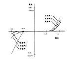
上記評価に関し、暗電流特性の結果を図2に示す。また、光照射時の電流電圧特性(開放起電力、短絡電流密度、光電変換効率)の結果を表1に示す。 Regarding the above evaluation, the results of the dark current characteristics are shown in FIG. Table 1 shows the results of current-voltage characteristics (open electromotive force, short-circuit current density, photoelectric conversion efficiency) during light irradiation.
図2に示されるように、実施例1の色素増感型太陽電池は、比較例1及び2の色素増感型太陽電池に比べて、暗電流の立ち上がりが鈍く、漏れ電流が少なかった。
また、ペルオキソチタン酸水溶液を用いた実施例1は、チタンイソプロポキシド溶液を用いた比較例2よりも、得られる漏れ電流抑制層の厚さが薄く、さらに漏れ電流抑制効果にも優れていた。
さらに、表1に示されるように、実施例1の色素増感型太陽電池は、比較例1及び2の色素増感型太陽電池に比べて、開放起電力、短絡電流密度及び光電変換効率が優れていた。
以上の結果からわかるように、本発明は、漏れ電流及び内部抵抗を抑制して光電変換効率の高い色素増感型太陽電池を製造することができる。
As shown in FIG. 2, the dye-sensitized solar cell of Example 1 had a slower dark current rise and less leakage current than the dye-sensitized solar cells of Comparative Examples 1 and 2.
In addition, Example 1 using a peroxotitanic acid aqueous solution had a thinner leakage current suppression layer and a superior leakage current suppression effect than Comparative Example 2 using a titanium isopropoxide solution. .
Furthermore, as shown in Table 1, the dye-sensitized solar cell of Example 1 has an open electromotive force, a short-circuit current density, and a photoelectric conversion efficiency as compared with the dye-sensitized solar cells of Comparative Examples 1 and 2. It was excellent.
As can be seen from the above results, the present invention can produce a dye-sensitized solar cell with high photoelectric conversion efficiency by suppressing leakage current and internal resistance.
1 透明基板、2 導電体層、3 漏れ電流抑制層、4 半導体層、5 電解質、6 対向電極、7 半導体電極。 DESCRIPTION OF SYMBOLS 1 Transparent substrate, 2 Conductor layer, 3 Leakage current suppression layer, 4 Semiconductor layer, 5 Electrolyte, 6 Counter electrode, 7 Semiconductor electrode.
Claims (5)
Priority Applications (1)
| Application Number | Priority Date | Filing Date | Title |
|---|---|---|---|
| JP2006017939A JP2007200714A (en) | 2006-01-26 | 2006-01-26 | Dye-sensitized solar cell and its manufacturing method |
Applications Claiming Priority (1)
| Application Number | Priority Date | Filing Date | Title |
|---|---|---|---|
| JP2006017939A JP2007200714A (en) | 2006-01-26 | 2006-01-26 | Dye-sensitized solar cell and its manufacturing method |
Publications (1)
| Publication Number | Publication Date |
|---|---|
| JP2007200714A true JP2007200714A (en) | 2007-08-09 |
Family
ID=38455112
Family Applications (1)
| Application Number | Title | Priority Date | Filing Date |
|---|---|---|---|
| JP2006017939A Pending JP2007200714A (en) | 2006-01-26 | 2006-01-26 | Dye-sensitized solar cell and its manufacturing method |
Country Status (1)
| Country | Link |
|---|---|
| JP (1) | JP2007200714A (en) |
Cited By (4)
| Publication number | Priority date | Publication date | Assignee | Title |
|---|---|---|---|---|
| JP2008210713A (en) * | 2007-02-27 | 2008-09-11 | Jgc Catalysts & Chemicals Ltd | Photoelectric cell, and method of manufacturing the same |
| JP2011065751A (en) * | 2009-09-15 | 2011-03-31 | Ricoh Co Ltd | Photoelectric conversion element |
| CN102332356A (en) * | 2010-06-25 | 2012-01-25 | 索尼公司 | DSSC and manufacturing approach thereof |
| JP2016082005A (en) * | 2014-10-14 | 2016-05-16 | 積水化学工業株式会社 | Method for manufacturing organic inorganic hybrid solar battery, and organic inorganic hybrid solar battery |
-
2006
- 2006-01-26 JP JP2006017939A patent/JP2007200714A/en active Pending
Cited By (5)
| Publication number | Priority date | Publication date | Assignee | Title |
|---|---|---|---|---|
| JP2008210713A (en) * | 2007-02-27 | 2008-09-11 | Jgc Catalysts & Chemicals Ltd | Photoelectric cell, and method of manufacturing the same |
| JP2011065751A (en) * | 2009-09-15 | 2011-03-31 | Ricoh Co Ltd | Photoelectric conversion element |
| CN102332356A (en) * | 2010-06-25 | 2012-01-25 | 索尼公司 | DSSC and manufacturing approach thereof |
| JP2012028302A (en) * | 2010-06-25 | 2012-02-09 | Sony Corp | Dye-sensitized solar cell and method for manufacturing the same |
| JP2016082005A (en) * | 2014-10-14 | 2016-05-16 | 積水化学工業株式会社 | Method for manufacturing organic inorganic hybrid solar battery, and organic inorganic hybrid solar battery |
Similar Documents
| Publication | Publication Date | Title |
|---|---|---|
| JP5023866B2 (en) | Dye-sensitized photoelectric conversion element, method for producing the same, and electronic device | |
| JP4909256B2 (en) | Modified titanium oxide fine particles and photoelectric conversion element using the same | |
| JP5428555B2 (en) | Method for producing dye-sensitized photoelectric conversion element | |
| JP5081345B2 (en) | Method for manufacturing photoelectric conversion element | |
| KR20080094021A (en) | Dye sensitization photoelectric converter | |
| US20030230335A1 (en) | Methods for producing titanium oxide sol and fine titanium oxide particles, and photoelectric conversion device | |
| EP2530779A1 (en) | Electrolyte solution for dye sensitized solar cell, and dye sensitized solar cell using same | |
| JP2008071535A (en) | Photoelectric conversion element and its manufacturing method | |
| JP2003297443A (en) | Photoelectric conversion oxide semiconductor electrode and dye-sensitized solar battery | |
| JP2009076369A (en) | Dye-sensitized solar cell | |
| JP2004161589A (en) | Method of manufacturing titanium oxide sol and titanium oxide fine particle, and photoelectric conversion device | |
| JP2008186669A (en) | Manufacturing method of dye-sensitized solar cell | |
| JP4356865B2 (en) | Method for producing metal-metal oxide composite electrode, photoelectric conversion element and photovoltaic cell | |
| TWI510497B (en) | An additive for an electrolyte composition and an electrolyte composition using the same and a dye-sensitized solar cell | |
| JP2007200714A (en) | Dye-sensitized solar cell and its manufacturing method | |
| JP2003297442A (en) | Photoelectric conversion oxide semiconductor electrode and dye-sensitized solar battery | |
| JP2012051952A (en) | Pigment, photoelectric element and photoelectrochemical battery | |
| KR20100066158A (en) | Novel organic dye incorporating a trialkoxysilyl and preparation thereof | |
| JP2007213959A (en) | Photoelectric conversion element | |
| JP2004124124A (en) | Method for manufacturing metal-metal oxide compound electrode, photoelectric transducer, and photoelectric cell | |
| JP2007188809A (en) | Gel electrolyte, photoelectric conversion element and solar cell | |
| JP4931402B2 (en) | Photoelectric conversion element | |
| JP2004238213A (en) | Method of manufacturing titanium oxide particle and photoelectric conversion device using the same | |
| JP2011165615A (en) | Photoelectric conversion element and method of manufacturing the same | |
| JP5566681B2 (en) | Electrolyte composition for photoelectric conversion element and photoelectric conversion element |