JP2007200230A - Touch panel, electro-optical device and electronic equipment - Google Patents
Touch panel, electro-optical device and electronic equipment Download PDFInfo
- Publication number
- JP2007200230A JP2007200230A JP2006020930A JP2006020930A JP2007200230A JP 2007200230 A JP2007200230 A JP 2007200230A JP 2006020930 A JP2006020930 A JP 2006020930A JP 2006020930 A JP2006020930 A JP 2006020930A JP 2007200230 A JP2007200230 A JP 2007200230A
- Authority
- JP
- Japan
- Prior art keywords
- touch panel
- substrate
- surface acoustic
- acoustic wave
- substrates
- Prior art date
- Legal status (The legal status is an assumption and is not a legal conclusion. Google has not performed a legal analysis and makes no representation as to the accuracy of the status listed.)
- Withdrawn
Links
Images


Abstract
Description
本発明は、タッチパネル、電気光学装置及び電子機器に関する。 The present invention relates to a touch panel, an electro-optical device, and an electronic apparatus.
表面弾性波(SAW)タッチパネルは、一般的に、可撓性を有するタッチパネル基板と、このタッチパネル基板に対向する対向基板とを主体として構成されている。これら対向する基板のうち一方の基板(例えば対向基板)の対向面には、表面弾性波を発生させる送信側トランスデューサと、その表面弾性波を受信する受信側トランスデューサとが設けられている。 A surface acoustic wave (SAW) touch panel is generally composed mainly of a flexible touch panel substrate and a counter substrate facing the touch panel substrate. A transmitting-side transducer that generates surface acoustic waves and a receiving-side transducer that receives the surface acoustic waves are provided on the opposing surface of one of the opposing substrates (for example, the opposing substrate).
送信側トランスデューサから発信された表面弾性波は、対向基板上を伝播して受信側トランスデューサで受信される。対向基板上に表面弾性波の伝播を阻害する阻害物があると、その部分で表面弾性波が弱められ、受信側トランスデューサで受信される表面弾性波の波形は阻害物の部分が減衰した状態になる。 The surface acoustic wave transmitted from the transmission side transducer propagates on the counter substrate and is received by the reception side transducer. If there is an obstacle that inhibits the propagation of surface acoustic waves on the opposing substrate, the surface acoustic wave is weakened at that part, and the waveform of the surface acoustic wave received by the receiving transducer is in a state where the part of the obstacle is attenuated. Become.
ユーザがタッチパネル基板をタッチすることで当該タッチパネル基板が撓み、対向基板に接触する。対向基板に接触したタッチパネル基板は、表面弾性波の阻害物となり、この部分で表面弾性波が減衰する。受信側トランスデューサでは、受信された表面弾性波の波形から減衰波形が出現するまでの時間が測定され、当該測定値に基いてパネル上のXY座標が算出され、ユーザがタッチした位置が検出される。 When the user touches the touch panel substrate, the touch panel substrate bends and contacts the counter substrate. The touch panel substrate in contact with the counter substrate becomes an obstacle to surface acoustic waves, and the surface acoustic waves are attenuated at this portion. The receiving-side transducer measures the time from the received surface acoustic wave waveform until the attenuation waveform appears, calculates the XY coordinates on the panel based on the measured value, and detects the position touched by the user. .
このように構成されたSAWタッチパネルは、表示パネルと組み合わされて、ワードプロセッサやATMなど、さまざまな機器の表示部として搭載されており、近年では、PDA(Personal Digital Assistant)やパームトップコンピュータなどの携帯型電子機器の表示部として搭載することが検討されている。 The SAW touch panel configured as described above is combined with a display panel and mounted as a display unit of various devices such as a word processor and an ATM. It is considered to be mounted as a display unit of a type electronic device.
一方で、携帯型電子機器は振動や衝撃を頻繁に受ける。SAWタッチパネルはパネルがむき出しの構成になっているため、振動や衝撃などによってパネルが欠けたり割れたりしやすく、これによりガラスが飛散してしまうという問題がある。この問題に対しては、パネルの保護及び破片の飛散防止のため、タッチパネルの表面、例えばユーザがタッチする面に保護フィルムを設けた構成のSAWタッチパネルが知られている(例えば、特許文献1及び特許文献2を参照)。
しかしながら、特許文献1及び特許文献2に記載の構成においては、樹脂フィルムの材質によっては、ユーザがタッチしたときの阻害物として十分に機能せず、表面弾性波を十分に減衰させることができない場合がある。このため、減衰波形が出現するまでの時間を測定するのが困難になり、位置検出能力が低下してしまうという問題がある。
以上のような事情に鑑み、本発明の目的は、高い位置検出能力を有するタッチパネル、電気光学装置及び電子機器を提供することにある。
However, in the configurations described in Patent Document 1 and Patent Document 2, depending on the material of the resin film, it does not function sufficiently as an obstacle when the user touches, and the surface acoustic wave cannot be sufficiently attenuated. There is. For this reason, it becomes difficult to measure the time until the attenuation waveform appears, and there is a problem that the position detection capability is lowered.
In view of the circumstances as described above, an object of the present invention is to provide a touch panel, an electro-optical device, and an electronic apparatus having a high position detection capability.
上記目的を達成するため、本発明に係るタッチパネルは、互いに対向配置されるとともに少なくとも一方が可撓性を有し、当該可撓性によって変形したときに互いに接触可能に配置された一対の基板と、前記一対の基板のうち一方の基板における他方の基板との対向する面上に表面弾性波を発生させる表面弾性波発生手段と、前記表面弾性波発生手段により発生し前記一方の基板から前記他方の基板に伝播した前記表面弾性波を検知する表面弾性波検知手段と、前記表面弾性波検知手段によって検知された前記表面弾性波の波形に基づいて、前記一対の基板の押圧された位置を検出する位置検出手段とを具備することを特徴とする。 In order to achieve the above object, a touch panel according to the present invention includes a pair of substrates that are arranged so as to face each other and at least one of them is flexible and can be brought into contact with each other when deformed by the flexibility. A surface acoustic wave generating means for generating a surface acoustic wave on a surface of one of the pair of substrates facing the other substrate; and the surface acoustic wave generating means that generates the surface acoustic wave from the one substrate to the other. A surface acoustic wave detecting means for detecting the surface acoustic wave propagated to the substrate, and the pressed positions of the pair of substrates are detected based on the surface acoustic wave waveform detected by the surface acoustic wave detecting means. And a position detection means.
本発明の構成によれば、一対の基板のうち可撓性を有する基板が押圧されると、当該押圧された基板が撓んで、一方の基板と他方の基板とが接触する。このとき、表面弾性波発生手段によって一対の基板のうち一方の基板の対向面に発生している表面弾性波が、接触部分を介して他方の基板へと伝播し、表面弾性波検知手段によって検知されることになる。つまり、本発明では、接触部分からの表面弾性波のみが表面弾性波検知手段によって検知されることになる。 According to the configuration of the present invention, when a flexible substrate of a pair of substrates is pressed, the pressed substrate is bent, and one substrate and the other substrate are in contact with each other. At this time, the surface acoustic wave generated on the opposing surface of one of the pair of substrates by the surface acoustic wave generating means propagates to the other substrate through the contact portion, and is detected by the surface acoustic wave detecting means. Will be. That is, in the present invention, only the surface acoustic wave from the contact portion is detected by the surface acoustic wave detection means.
従来のタッチパネルでは、阻害物が無い状態の表面弾性波の波形データを記憶させ、当該波形データと比較することで波形の減衰部分を検出する必要があったため、減衰部分が小さい場合には十分に検出できない虞があった。これに対して、本発明では、一対の基板の一方の基板と他方の基板との接触部分から伝播する表面弾性波のみを検知する構成になっているので、表面弾性波を検知できれば、表面弾性波の波形に関わらず接触部分の位置(押圧された位置)を特定することができる。これにより、高い検出能力を確保することができる。 In the conventional touch panel, it was necessary to store the waveform data of the surface acoustic wave without any obstruction and to detect the attenuation part of the waveform by comparing with the waveform data. There was a possibility that it could not be detected. On the other hand, in the present invention, since only the surface acoustic wave propagating from the contact portion between one substrate and the other substrate of the pair of substrates is detected, if the surface acoustic wave can be detected, the surface elasticity The position (pressed position) of the contact portion can be specified regardless of the waveform of the wave. Thereby, a high detection capability can be ensured.
また、前記表面弾性波発生手段は、前記一方の基板における前記他方の基板と対向する面上に設けられた送信側トランスデューサであり、前記表面弾性波受信手段は、前記他方の基板における前記一方の基板と対向する面上に設けられた受信側トランスデューサであることが好ましい。
本発明によれば、表面弾性波発生手段である送信側トランスデューサが一方の基板に設けられており、表面弾性波受信手段である受信側トランスデューサが他方の基板に設けられているので、送信側トランスデューサと受信側トランスデューサとを平面視で重なるように配置することができる。従来では、送信側トランスデューサと受信側トランスデューサとが同一の基板上に配置されていたので、両者を平面的にずらして配置する必要があったが、本発明では、両者を平面視で重なるように配置することができ、これにより、基板内のスペースを広く確保することができる。
The surface acoustic wave generating means is a transmission-side transducer provided on a surface of the one substrate facing the other substrate, and the surface acoustic wave receiving means is the one of the other substrates. It is preferable that it is a receiving side transducer provided on the surface facing the substrate.
According to the present invention, the transmitting-side transducer that is the surface acoustic wave generating means is provided on one substrate, and the receiving-side transducer that is the surface acoustic wave receiving means is provided on the other substrate. And the receiving-side transducer can be arranged so as to overlap in plan view. Conventionally, since the transmission-side transducer and the reception-side transducer are arranged on the same substrate, it is necessary to dispose them both in a plane, but in the present invention, both are overlapped in a plan view. Therefore, a large space in the substrate can be secured.
また、前記表面弾性波発生手段から発生された表面弾性波を前記一対の基板の中央部に伝播させる反射電極を更に設けることが好ましい。
本発明によれば、表面弾性波発生手段から発生された表面弾性波を一対の基板の中央部に伝播させる反射電極を更に設けることとしたので、表面弾性波を基板の中央部に容易に伝播させることができる。
Moreover, it is preferable to further provide a reflective electrode for propagating the surface acoustic wave generated from the surface acoustic wave generating means to the central part of the pair of substrates.
According to the present invention, since the reflection electrode for propagating the surface acoustic wave generated from the surface acoustic wave generating means to the central portion of the pair of substrates is further provided, the surface acoustic wave is easily propagated to the central portion of the substrate. Can be made.
また、前記一対の基板の押圧される面に樹脂フィルムが設けられていることが好ましい。
本発明によれば、一対の基板の押圧される面に樹脂フィルムが設けられているので、当該一対の基板の一つ又は双方が破損した場合であっても破片が飛散するのを防ぐことができる。
Moreover, it is preferable that the resin film is provided in the surface pressed by a pair of said board | substrate.
According to the present invention, since the resin film is provided on the pressed surfaces of the pair of substrates, it is possible to prevent the fragments from scattering even when one or both of the pair of substrates are damaged. it can.
また、前記一対の基板の押圧される面に偏光板が設けられていることが好ましい。
本発明によれば、一対の基板の押圧される面に偏光板が設けられているので、例えば当該押圧される基板に対向する基板が破損した場合であっても破片が飛散するのを防ぐことができる。
Moreover, it is preferable that a polarizing plate is provided on the surface to be pressed of the pair of substrates.
According to the present invention, since the polarizing plate is provided on the surfaces to be pressed of the pair of substrates, for example, even if the substrate facing the pressed substrate is damaged, the fragments are prevented from scattering. Can do.
本発明に係る電気光学装置は、上記のタッチパネルと、前記タッチパネルに対向して設けられ、画像を表示する表示パネルとを具備することを特徴とする。
本発明によれば、高い位置検出能力を有するタッチパネルが設けられた電気光学装置を得ることができる。
An electro-optical device according to the present invention includes the above-described touch panel and a display panel that is provided to face the touch panel and displays an image.
According to the present invention, an electro-optical device provided with a touch panel having high position detection capability can be obtained.
また、前記タッチパネルを構成する前記一対の基板のうち一方が、前記表示パネルの基板を兼ねていることが好ましい。
本発明によれば、タッチパネルを構成する一対の基板のうち一方が、表示基板を兼ねているので、別途基板を設ける必要が無い。これにより、電気光学装置を薄型化することができる。
Further, it is preferable that one of the pair of substrates constituting the touch panel also serves as the substrate of the display panel.
According to the present invention, since one of the pair of substrates constituting the touch panel also serves as the display substrate, it is not necessary to provide a separate substrate. Thereby, the electro-optical device can be thinned.
本発明に係る電子機器は、上記の電気光学装置を搭載したことを特徴とする。
本発明によれば、位置検出能力の高いタッチパネルを有する電子機器を得ることができる。
An electronic apparatus according to the present invention includes the above-described electro-optical device.
According to the present invention, an electronic device having a touch panel with high position detection capability can be obtained.
本発明の実施の形態を図面に基き説明する。以下の図では、各部材を認識可能な大きさとするため、縮尺を適宜変更している。
[第1実施形態]
まず、本発明の第1実施形態に係るタッチパネル付きの液晶装置を説明する。図1は、タッチパネル付き液晶装置1の構成を示す断面図である。
Embodiments of the present invention will be described with reference to the drawings. In the following drawings, the scale is appropriately changed to make each member a recognizable size.
[First Embodiment]
First, a liquid crystal device with a touch panel according to a first embodiment of the present invention will be described. FIG. 1 is a cross-sectional view illustrating a configuration of a liquid crystal device 1 with a touch panel.
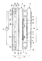
図1に示すように、液晶装置1は、液晶パネル2とタッチパネル3とを主体として構成されており、液晶パネル2とタッチパネル3とが対向して貼り合わされた構成になっている。本実施形態では、液晶装置1を駆動するスイッチング素子として薄膜トランジスタ(Thin Film Transistor、以下TFTという)素子を用いたアクティブマトリクス方式の液晶装置を例に挙げて説明する。また、本実施形態では、タッチパネル3としてシェブロン型トランスデューサタイプのタッチパネルを例に挙げて説明する。 As shown in FIG. 1, the liquid crystal device 1 is mainly configured by a liquid crystal panel 2 and a touch panel 3, and the liquid crystal panel 2 and the touch panel 3 are bonded to face each other. In the present embodiment, an active matrix type liquid crystal device using a thin film transistor (hereinafter referred to as TFT) element as a switching element for driving the liquid crystal device 1 will be described as an example. In this embodiment, a chevron transducer type touch panel will be described as an example of the touch panel 3.
まず、液晶パネル2の構成を説明する。液晶パネル2は、TFTアレイ基板4とカラーフィルタ基板5とがシール材7によって貼り合わされ、このシール材7によって区画された領域内に液晶層6が封入された構成になっている。シール材7の内部にはギャップ材8が設けられており、当該ギャップ材8によってTFTアレイ基板4とカラーフィルタ基板5との間にギャップが形成されている。シール材7で囲まれた領域は、画像や動画等を表示する表示領域9になっている。
First, the configuration of the liquid crystal panel 2 will be described. The liquid crystal panel 2 has a configuration in which a TFT array substrate 4 and a
TFTアレイ基板4は、例えばガラスや石英等の透光性の高い材料から形成された基材4aを主体として構成されており、この基材4aの液晶側には、画素電極18と、この画素電極18を駆動するTFT素子17と、当該TFT素子17に電気信号を伝達するデータ線(図示せず)及び走査線15と、これら画素電極18、TFT素子17、データ線及び走査線15を覆うように形成された配向膜16とが設けられている。画素電極18は、例えばITO(Indium Tin Oxide)等の透明な導電材料によって形成されている。また、TFTアレイ基板4の外側(液晶層6とは反対側)の面には、偏光板19が貼り付けられている。
The TFT array substrate 4 is mainly composed of a
カラーフィルタ基板5は、TFTアレイ基板4と同様にガラスや石英等の透光性の高い材料からなる基材5aを主体として構成されている。基材5aの液晶6側には、例えば赤色層、緑色層、青色層の3色の色層からなるカラーフィルタ層20が形成され、当該カラーフィルタ層20の周囲にはブラックマトリクス21が形成されている。また、カラーフィルタ層20及びブラックマトリクス21を覆うように共通電極28が形成されており、当該共通電極28上を配向膜26が覆っている。共通電極28は、画素電極18と同様、例えばITO等の透明な導電材料によって形成されている。カラーフィルタ基板5の外側の面には、偏光板29が貼付されている。
Similar to the TFT array substrate 4, the
液晶層6は、例えばフッ素系液晶化合物や非フッ素系液晶化合物等の液晶分子によって構成されており、TFTアレイ基板4側の配向膜16とカラーフィルタ基板5側の配向膜26との双方に接するように両基板に挟持されている。液晶分子の配向は、非選択電圧を印加したときに所定の方向に向くように、配向膜16及び配向膜26によって規制されている。
The
また、本実施形態では図示を省略するが、TFTアレイ基板4側にはバックライトが設けられており、当該バックライトの光がTFTアレイ基板4、液晶層6、カラーフィルタ基板5を透過することによって、カラーフィルタ基板5側に画像(文字や動画などを含む)が表示されるようになっている。すなわち、本実施形態では、カラーフィルタ基板5側が表示面側である。
Although not shown in the present embodiment, a backlight is provided on the TFT array substrate 4 side, and the light from the backlight passes through the TFT array substrate 4, the
次に、タッチパネル3の構成を説明する。タッチパネル3は、表面弾性波式の反射電極タイプのタッチパネルであり、タッチパネル基板31と対向基板32とがシール材33によって貼り合わされた構成になっている。タッチパネル3は、液晶パネル2の表示面側(カラーフィルタ基板5側)に配置されており、当該液晶パネル2の表示面と対向するように貼り付けられている。タッチパネル基板31と対向基板32との間にはスペーサ36が配置されており、両基板の間が所定の間隔に保持されている。
Next, the configuration of the touch panel 3 will be described. The touch panel 3 is a surface acoustic wave reflective electrode type touch panel, and has a configuration in which a
タッチパネル基板31は、ユーザが直接あるいはペンなどによってタッチする基板であり、当該ユーザのタッチによって撓む程度の可撓性を有している。このタッチパネル基板31は、例えば透光性の高い樹脂材料によってフィルム状に形成されている。タッチパネル基板31の外面31aには、ポリイミドなどの透明な樹脂材料によって形成された樹脂フィルム40が貼り付けられている。
The
対向基板32は、例えばガラスや石英、プラスチックなどの透光性の高い材料によって形成された基板であり、タッチパネル基板31と対向して設けられている。また、当該対向基板32の外面32aが液晶パネルの表示面側の偏光板29上に貼り付けられた状態になっている。
The
タッチパネル基板31の内面31b及び対向基板32の内面32bには、送信側トランスデューサ34及び受信側トランスデューサ35が設けられている。送信側トランスデューサ34は内面31bと内面32bに1つずつ、受信側トランスデューサ35も内面31bと内面32bに1つずつ、それぞれ設けられている。送信側トランスデューサ34は、内面31b及び内面32bに表面弾性波を発生させる表面弾性波発生手段である。受信側トランスデューサ35は、表面弾性波を検知する表面弾性波検知手段である。
On the
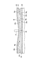
図2は、送信側トランスデューサ34及び受信側トランスデューサ35の平面配置を示す平面図である。図中、タッチパネル3の長手方向をX方向、短手方向をY方向として説明する。また、図中実線部分がタッチパネル基板31側の構成を、図中破線部分が対向基板32側の構成を、それぞれ示すものとする。
FIG. 2 is a plan view showing a planar arrangement of the
図2に示すように、送信側トランスデューサ34は、図2中タッチパネル3の左上角部及び右下角部に1つずつ、計2つ設けられている。図2中左上角部の送信側トランスデューサ34xは、タッチパネル基板31の内面31b(図1参照)に設けられている。この送信側トランスデューサ34xは、タッチパネル基板31の内面31bに図2中下向きに伝播する表面弾性波Wxを発生させる。この表面弾性波Wxはタッチパネル基板31の左辺側に配列された反射電極37aで反射され、タッチパネル3の中央部の伝播領域50をX方向に、図中右側へ向けて伝播する。
As shown in FIG. 2, a total of two transmission-
図2中右下角部の送信側トランスデューサ34yは、対向基板32の内面32b(図1参照)に設けられている。この送信側トランスデューサ34yは、対向基板32の内面32bに図2中左向きに伝播する表面弾性波Wyを発生させる。この表面弾性波Wyは対向基板32の図2中下辺側に配列された反射電極38aによって反射され、タッチパネル3の中央部の伝播領域50をY方向に、図中上側へ向けて伝播する。
2 is provided on the
また、受信側トランスデューサ35は、図3中タッチパネル3の右上角部に2つとも設けられている。このうち、受信側トランスデューサ35xがタッチパネル基板31の内面31bに設けられており、受信側トランスデューサ35yが対向基板32の内面32bに設けられている。受信側トランスデューサ35xと受信側トランスデューサ35yとは、一部が平面視で重なるように配置されている。
Further, two receiving-
また、図1に示すように、送信側トランスデューサ34(34x、34y)及び受信側トランスデューサ35(35x、35y)は、コントロール回路41に電気的に接続されている。
図3を用いてコントロール回路41の構成を説明する。コントロール回路41は、図3に示すように、CPU42と、A/D変換回路43と、信号増幅部44と、バースト波形ドライバ45とを主体として構成されている。
As shown in FIG. 1, the transmission-side transducer 34 (34x, 34y) and the reception-side transducer 35 (35x, 35y) are electrically connected to the
The configuration of the
バースト波形ドライバ45は、タッチパネル3の送信側トランスデューサ34x、34yにそれぞれ接続されており、送信側トランスデューサ34x、34yにて発生させる表面弾性波の波形及び表面弾性波を発生させるタイミングをコントロールする。信号増幅器44(44x、44y)は、受信側トランスデューサ35x、35yからの信号を増幅する。A/D変換回路43(43x、43y)は、信号増幅器44からの信号をA/D変換してCPU42に送出する。
The
CPU42は、A/D変換回路43を制御すると共に、当該A/D変換回路43を介して受信側トランスデューサ35から送信された信号を受信し、当該信号に基いてタッチパネル3上で押圧された位置を検出する。また、バースト波形ドライバ45へ信号を送出して、当該バースト波形ドライバ45を制御する。
The
次に、ユーザがタッチパネル3にタッチしたときの動作を説明する。
例えば図4に示すように、ユーザがペンPなどで樹脂フィルム40を介してタッチパネル基板31にタッチすると、タッチパネル基板31が図4中下側に撓み、タッチパネル基板31の内面31bが対向基板32の内面32bに接触する。以下、両基板の内面31b、32bが接触する部分を「接触部分39」という。送信側トランスデューサ34xによってタッチパネル基板31の内面31bに発生した表面弾性波Wxは、この接触部分39を介して、対向基板32の内面32bへ伝播する。
Next, an operation when the user touches the touch panel 3 will be described.
For example, as shown in FIG. 4, when the user touches the
対向基板32の内面32bへ伝播した表面弾性波Wxは、図2に示すように、当該内面32bを接触部分39から図2中右側に伝播し、対向基板32の右辺側に配列された反射電極37bによって反射され、当該右辺を図2中上側へ伝播する。この表面弾性波Wxは、対向基板32側に設けられた受信側トランスデューサ35xによって検知される。
As shown in FIG. 2, the surface acoustic wave Wx propagated to the
また、送信側トランスデューサ34yによって対向基板32の内面32bに発生した表面弾性波Wyは、この接触部分39を介して、タッチパネル基板31の内面31bへ伝播する。内面31bへ伝播した表面弾性波Wyは、図2に示すように、タッチパネル基板31の内面31bを接触部分39から図2中上側へ伝播し、タッチパネル基板31の上辺側に配列された反射電極38bによって反射されて、当該上辺を図2中右側へ伝播する。この表面弾性波Wyは、タッチパネル31側に設けられた受信側トランスデューサ35yによって検知される。
Further, the surface acoustic wave Wy generated on the
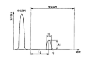
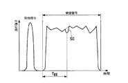
図5は、受信側トランスデューサ35x、35yによって検知された表面弾性波Wx、Wyの包絡線波形を示す図である。グラフの横軸は時間を示しており、縦軸は表面弾性波の強さを示している。
同図に示すように、表面弾性波Wx、Wyの包絡線波形のグラフでは、ある時間t1に亘って大きさA1の信号Sが発生している。上述したコントロール回路41のCPU42は、ユーザがタッチパネル3にタッチしてから信号Sを受信するまでの時間Tgを測定し、当該時間Tgに基いてタッチパネル基板31上のX方向及びY方向の位置を算出し、タッチされた場所のXY座標を特定する。
FIG. 5 is a diagram illustrating envelope waveforms of the surface acoustic waves Wx and Wy detected by the receiving-
As shown in the figure, in the graph of the envelope waveform of the surface acoustic waves Wx and Wy, the signal S having the magnitude A1 is generated over a certain time t1. The
このように、本実施形態では、タッチパネル基板31が押圧されると、当該タッチパネル基板31が撓んで、対向基板32に接触する。このとき、送信側トランスデューサ34によって発生した表面弾性波Wx、Wyは、接触部分39を介してそれぞれ他方の基板へと伝播し、他方の基板側に配置された受信側トランスデューサ35によって検知されることになる。つまり、本実施形態では、接触部分39から他方の基板に伝播した表面弾性波のみが検知されることになる。
Thus, in this embodiment, when the
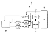
従来のタッチパネルでは、図6に示すように、送信側トランスデューサ64と受信側トランスデューサ65とが同一の基板(例えば、対向基板62)の内面に配置されていた。このため、ユーザがタッチパネル基板61をタッチすることで対向基板62に接触した接触部分69において、タッチパネル基板61は表面弾性波の阻害物となり、この部分を伝播する表面弾性波が減衰する。減衰した表面弾性波は、図7に示す減衰部分S0として検出される。図8に示すコントロール回路51のCPU52は、ユーザがタッチパネルにタッチしてから信号S0を受信するまでの時間Tggを測定し、当該時間Tggに基いてタッチパネル基板上のX方向及びY方向の位置を算出し、タッチされた場所のXY座標を特定する、という構成になっていた。
In the conventional touch panel, as shown in FIG. 6, the transmission-
この場合、例えば図8に示すように、阻害物が無い状態の表面弾性波の波形データをメモリ56に記憶させ、比較回路57によって当該波形データの波形と受信波形とを比較することで波形の減衰部分を検出する必要があったため、コントロール回路51の構成が複雑になっていた。また、図7に示すように、障害物が無い状態であっても受信波形の形状が平坦ではないため、減衰部分が小さい場合には十分に検出できない虞があった。
In this case, for example, as shown in FIG. 8, the waveform data of the surface acoustic wave in the absence of an obstacle is stored in the
これに対して、本実施形態によれば、タッチパネル基板31と対向基板32との接触部分39から伝播する表面弾性波Wx、Wyのみを検知する構成になっているので、表面弾性波Wx、Wyを検知できれば、接触部分39の位置(押圧された位置)のXY座標を特定することができる。これにより、高い検出能力を確保することができる。
On the other hand, according to the present embodiment, since only the surface acoustic waves Wx and Wy propagating from the
また、従来では、図6に示すように、送信側トランスデューサ64と受信側トランスデューサ65とがすべて同一の基板上にあったため、受信側トランスデューサ65を基板の角部に重ねて配置することができず、ずらして配置する必要があった。このため、例えば図6中右辺側の反射電極67と、図6中上辺側の反射電極68とについては、基板の内側に配置せざるを得なかった。
Further, conventionally, as shown in FIG. 6, since the transmission-
これに対して、本実施形態によれば、受信側トランスデューサ35xと受信側トランスデューサ35yとが平面視で重なるように配置されているので、反射電極37、38をタッチパネルの外辺に沿って配列させることができる。これにより、伝播領域50を広く確保できる。
On the other hand, according to the present embodiment, the receiving-
[第2実施形態]
次に、本発明の第2実施形態を説明する。第1実施形態と同様、以下の図では、各部材を認識可能な大きさとするため、縮尺を適宜変更している。また、第1実施形態と同一の構成要素については、その説明を省略する。
[Second Embodiment]
Next, a second embodiment of the present invention will be described. Similar to the first embodiment, in the following drawings, the scale is appropriately changed to make each member a recognizable size. The description of the same components as those in the first embodiment is omitted.
図9は、本実施形態に係るタッチパネル付き液晶装置101の構成を示す断面図である。
図9に示すように、液晶装置101は、液晶パネル102とタッチパネル103とを主体として構成されており、第1実施形態と同様、液晶パネル102とタッチパネル103とが対向した構成になっている。
FIG. 9 is a cross-sectional view showing the configuration of the
As shown in FIG. 9, the
本実施形態では、タッチパネル103のタッチパネル基板131に、上記樹脂フィルムの代わりに液晶パネル102の偏光板が貼り付けられた構成になっている。また、タッチパネル103の対向基板が、液晶パネル102のカラーフィルタ基板105aを兼ねた構成になっている。その他の構成は第1実施形態と同様である。
In the present embodiment, the polarizing plate of the
このように、本実施形態によれば、液晶パネル102の偏光板がタッチパネル103のタッチパネル基板131に貼り付けられた構成になっている、すなわち、第1実施形態の樹脂フィルムが偏光板を兼ねた構成になっているため、タッチパネル基板131が破損してもその破片が飛散するのを防ぐことができる。これにより、樹脂フィルムを別途設ける必要が無く、液晶装置101を薄型化することが可能となる。
As described above, according to the present embodiment, the polarizing plate of the
また、タッチパネル103の対向基板が、液晶パネル102のカラーフィルタ基板105aを兼ねた構成になっているので、第1実施形態に対して対向基板及びカラーフィルタ基板のいずれか一方を設けなくても済む。これにより、液晶装置101を更に薄型化することができる。
In addition, since the counter substrate of the
[電子機器]
以下、上述の電気光学装置を備えた電子機器の具体例について説明する。
図10は、本発明の電子機器の一例であるハンディターミナル1000を示す斜視図である。図10において、符号1001は本発明の入力装置であるタッチパネル、符号1002はファンクションキー、符号1003は電源入力スイッチをそれぞれ示している。本例のハンディターミナル1000は、ファンクションキー1002に印刷されたアイコンや、タッチパネル1001の下に配置された液晶パネル(図示略)の画面を見ながら、タッチパネル上の位置を直接指示することによって、データ入力を行なうものである。このハンディターミナル1000は、入力装置として前述した本発明のタッチパネルを備えているため、高い位置検出能力を有する電子機器となる。
[Electronics]
Hereinafter, specific examples of the electronic apparatus including the above-described electro-optical device will be described.
FIG. 10 is a perspective view showing a handy terminal 1000 which is an example of the electronic apparatus of the present invention. In FIG. 10,
本発明の技術範囲は上記実施形態に限定されるものではなく、本発明の趣旨を逸脱しない範囲で適宜変更を加えることができる。
例えば、上記実施形態では、タッチパネル3として、反射電極タイプのタッチパネルを例に挙げて説明したが、これに限られることは無く、例えば階段型トランスデューサタイプのタッチパネルや、シェブロン型トランスデューサタイプのタッチパネルなどのSAWタッチパネルにも適用することができる。
The technical scope of the present invention is not limited to the above-described embodiment, and appropriate modifications can be made without departing from the spirit of the present invention.
For example, in the above-described embodiment, the reflective electrode type touch panel has been described as an example of the touch panel 3, but the present invention is not limited to this. For example, a staircase type transducer type touch panel, a chevron type transducer type touch panel, etc. It can also be applied to a SAW touch panel.
また、上記実施形態において、表示パネルとして液晶パネルを例に挙げて説明したが、これに限られることは無く、例えば有機EL、PDP、CRTなどを用いても構わない。 In the above embodiment, the liquid crystal panel has been described as an example of the display panel. However, the present invention is not limited to this, and for example, an organic EL, PDP, CRT, or the like may be used.
さらに、上記実施形態では、2つの送信側トランスデューサ34及び2つの受信側トランスデューサ35がそれぞれタッチパネル基板31と対向基板32とに1つずつ配置された構成になっているが、これに限られることは無い。例えば、送信側トランスデューサ34を2つともタッチパネル基板31に配置し、受信側トランスデューサ35を2つとも対向基板32に配置する構成であっても、本発明の適用は可能になる。この場合、反射電極37a、38aをタッチパネル基板31側に配列すれば良い。あるいは、受信側トランスデューサ35を2つともタッチパネル基板31に配置し、送信側トランスデューサ34を2つとも対向基板32に配置しても良い。この場合は、反射電極37b、38bをタッチパネル基板31に配列すれば良い。また、これらの場合、送信側トランスデューサ34と受信側トランスデューサとを平面視で重なるように配置することによって、反射電極37a、37b、38a、38bを基板の外辺に沿って配列することができるので、伝播領域50を広く確保することができる。
Further, in the above-described embodiment, the two transmission-
1、101…液晶装置 2、102…液晶パネル 3、103…タッチパネル 31、131…タッチパネル基板 32…対向基板 34、134…送信側トランスデューサ 35、135…受信側トランスデューサ 1000…ハンディターミナル
DESCRIPTION OF
Claims (8)
前記一対の基板のうち一方の基板における他方の基板との対向する面上に表面弾性波を発生させる表面弾性波発生手段と、
前記表面弾性波発生手段により発生し前記一方の基板から前記他方の基板に伝播した前記表面弾性波を検知する表面弾性波検知手段と、
前記表面弾性波検知手段によって検知された前記表面弾性波の波形に基づいて、前記一対の基板の押圧された位置を検出する位置検出手段と
を具備することを特徴とするタッチパネル。 A pair of substrates that are arranged to face each other and at least one of them is flexible, and arranged so as to come into contact with each other when deformed by the flexibility;
A surface acoustic wave generating means for generating a surface acoustic wave on a surface of the one of the pair of substrates facing the other substrate;
Surface acoustic wave detection means for detecting the surface acoustic wave generated by the surface acoustic wave generation means and propagated from the one substrate to the other substrate;
A touch panel comprising: position detection means for detecting the pressed positions of the pair of substrates based on the waveform of the surface acoustic wave detected by the surface acoustic wave detection means.
前記表面弾性波受信手段は、前記他方の基板における前記一方の基板と対向する面上に設けられた受信側トランスデューサである
ことを特徴とする請求項1に記載のタッチパネル。 The surface acoustic wave generating means is a transmission-side transducer provided on a surface of the one substrate facing the other substrate,
The touch panel according to claim 1, wherein the surface acoustic wave receiving unit is a receiving-side transducer provided on a surface of the other substrate facing the one substrate.
ことを特徴とする請求項1乃至3のいずれか1項に記載のタッチパネル。 The touch panel according to any one of claims 1 to 3, wherein a resin film is provided on surfaces to be pressed of the pair of substrates.
前記タッチパネルに対向して設けられ、画像を表示する表示パネルと
を具備することを特徴とする電気光学装置。 A touch panel according to any one of claims 1 to 5,
An electro-optical device comprising: a display panel provided to face the touch panel and displaying an image.
ことを特徴とする請求項6に記載の電気光学装置。 The electro-optical device according to claim 6, wherein one of the pair of substrates constituting the touch panel also serves as a substrate of the display panel.
An electronic apparatus comprising the electro-optical device according to claim 6.
Priority Applications (1)
| Application Number | Priority Date | Filing Date | Title |
|---|---|---|---|
| JP2006020930A JP2007200230A (en) | 2006-01-30 | 2006-01-30 | Touch panel, electro-optical device and electronic equipment |
Applications Claiming Priority (1)
| Application Number | Priority Date | Filing Date | Title |
|---|---|---|---|
| JP2006020930A JP2007200230A (en) | 2006-01-30 | 2006-01-30 | Touch panel, electro-optical device and electronic equipment |
Publications (1)
| Publication Number | Publication Date |
|---|---|
| JP2007200230A true JP2007200230A (en) | 2007-08-09 |
Family
ID=38454751
Family Applications (1)
| Application Number | Title | Priority Date | Filing Date |
|---|---|---|---|
| JP2006020930A Withdrawn JP2007200230A (en) | 2006-01-30 | 2006-01-30 | Touch panel, electro-optical device and electronic equipment |
Country Status (1)
| Country | Link |
|---|---|
| JP (1) | JP2007200230A (en) |
Cited By (4)
| Publication number | Priority date | Publication date | Assignee | Title |
|---|---|---|---|---|
| JP2010027266A (en) * | 2008-07-16 | 2010-02-04 | Seiko Epson Corp | Electro-optical device and electron equipment |
| TWI471787B (en) * | 2012-04-06 | 2015-02-01 | Egalax Empia Technology Inc | Method and device for position detection |
| TWI475449B (en) * | 2012-04-06 | 2015-03-01 | Egalax Empia Technology Inc | Method and device for position detection |
| CN105843446A (en) * | 2016-03-18 | 2016-08-10 | 京东方科技集团股份有限公司 | Detection assembly, touch display apparatus, touch positioning method and pressure detection method |
-
2006
- 2006-01-30 JP JP2006020930A patent/JP2007200230A/en not_active Withdrawn
Cited By (5)
| Publication number | Priority date | Publication date | Assignee | Title |
|---|---|---|---|---|
| JP2010027266A (en) * | 2008-07-16 | 2010-02-04 | Seiko Epson Corp | Electro-optical device and electron equipment |
| TWI471787B (en) * | 2012-04-06 | 2015-02-01 | Egalax Empia Technology Inc | Method and device for position detection |
| TWI475449B (en) * | 2012-04-06 | 2015-03-01 | Egalax Empia Technology Inc | Method and device for position detection |
| CN105843446A (en) * | 2016-03-18 | 2016-08-10 | 京东方科技集团股份有限公司 | Detection assembly, touch display apparatus, touch positioning method and pressure detection method |
| CN105843446B (en) * | 2016-03-18 | 2019-10-25 | 京东方科技集团股份有限公司 | Detection components, touch control display apparatus, touch localization method and pressure detection method |
Similar Documents
| Publication | Publication Date | Title |
|---|---|---|
| JP4506742B2 (en) | Touch panel, electro-optical device and electronic apparatus | |
| JP4412288B2 (en) | Electro-optical device and electronic apparatus | |
| JP4412289B2 (en) | Electro-optical device and electronic apparatus | |
| JP5306059B2 (en) | Touch panel, display panel, touch panel substrate, display panel substrate, and display device | |
| KR100831487B1 (en) | Touch panel, method for detecting touch input position, electro-optic device, and electronic device | |
| JP5370944B2 (en) | Touch panel and manufacturing method thereof | |
| JP5520093B2 (en) | Manufacturing method of touch panel | |
| JP4198527B2 (en) | Touch panel and display device | |
| US20120081332A1 (en) | Display device equipped with touch panel | |
| US20110140720A1 (en) | Electrostatic capacitance-type input device, method of testing electrostatic capacitance-type input device, and driving device for electrostatic capacitance-type input device | |
| JP5082770B2 (en) | Touch panel, display device, electronic equipment | |
| JP2007200230A (en) | Touch panel, electro-optical device and electronic equipment | |
| JP2011154431A (en) | Input device and electrooptical device with the same | |
| JP4562578B2 (en) | Touch panel and touch panel type coordinate input method | |
| JP2006195316A (en) | Electro-optical device and electronic equipment | |
| JP2006243428A (en) | Display device, and method for manufacturing display device, liquid crystal display device, and method for manufacturing liquid crystal display device, electronic appliance | |
| JP2007264688A (en) | Touch panel, electro-optic device, and electronic appliance | |
| JPH07160417A (en) | Display integrated type tablet device | |
| JP2006343919A (en) | Electro-optic device and touch panel | |
| JP2007264686A (en) | Touch panel, electrooptical device and electronic equipment | |
| JP2006343920A (en) | Touch panel, electro-optical device, and electronic equipment | |
| JP4613858B2 (en) | Touch panel, electro-optical device and electronic apparatus | |
| JP2006343918A (en) | Electro-optic device, touch panel and method for controlling touch panel | |
| JP2007264687A (en) | Touch panel, electrooptic device and electronic equipment |
Legal Events
| Date | Code | Title | Description |
|---|---|---|---|
| A300 | Withdrawal of application because of no request for examination |
Free format text: JAPANESE INTERMEDIATE CODE: A300 Effective date: 20090407 |