JP2007178995A - Method for fabricating thin film pattern and method for fabricating flat panel display device using same - Google Patents
Method for fabricating thin film pattern and method for fabricating flat panel display device using same Download PDFInfo
- Publication number
- JP2007178995A JP2007178995A JP2006207623A JP2006207623A JP2007178995A JP 2007178995 A JP2007178995 A JP 2007178995A JP 2006207623 A JP2006207623 A JP 2006207623A JP 2006207623 A JP2006207623 A JP 2006207623A JP 2007178995 A JP2007178995 A JP 2007178995A
- Authority
- JP
- Japan
- Prior art keywords
- thin film
- film pattern
- substrate
- organic
- master mold
- Prior art date
- Legal status (The legal status is an assumption and is not a legal conclusion. Google has not performed a legal analysis and makes no representation as to the accuracy of the status listed.)
- Granted
Links
Images


Classifications
-
- G—PHYSICS
- G02—OPTICS
- G02F—OPTICAL DEVICES OR ARRANGEMENTS FOR THE CONTROL OF LIGHT BY MODIFICATION OF THE OPTICAL PROPERTIES OF THE MEDIA OF THE ELEMENTS INVOLVED THEREIN; NON-LINEAR OPTICS; FREQUENCY-CHANGING OF LIGHT; OPTICAL LOGIC ELEMENTS; OPTICAL ANALOGUE/DIGITAL CONVERTERS
- G02F1/00—Devices or arrangements for the control of the intensity, colour, phase, polarisation or direction of light arriving from an independent light source, e.g. switching, gating or modulating; Non-linear optics
- G02F1/01—Devices or arrangements for the control of the intensity, colour, phase, polarisation or direction of light arriving from an independent light source, e.g. switching, gating or modulating; Non-linear optics for the control of the intensity, phase, polarisation or colour
- G02F1/13—Devices or arrangements for the control of the intensity, colour, phase, polarisation or direction of light arriving from an independent light source, e.g. switching, gating or modulating; Non-linear optics for the control of the intensity, phase, polarisation or colour based on liquid crystals, e.g. single liquid crystal display cells
- G02F1/133—Constructional arrangements; Operation of liquid crystal cells; Circuit arrangements
- G02F1/136—Liquid crystal cells structurally associated with a semi-conducting layer or substrate, e.g. cells forming part of an integrated circuit
- G02F1/1362—Active matrix addressed cells
-
- G—PHYSICS
- G02—OPTICS
- G02F—OPTICAL DEVICES OR ARRANGEMENTS FOR THE CONTROL OF LIGHT BY MODIFICATION OF THE OPTICAL PROPERTIES OF THE MEDIA OF THE ELEMENTS INVOLVED THEREIN; NON-LINEAR OPTICS; FREQUENCY-CHANGING OF LIGHT; OPTICAL LOGIC ELEMENTS; OPTICAL ANALOGUE/DIGITAL CONVERTERS
- G02F2202/00—Materials and properties
- G02F2202/02—Materials and properties organic material
- G02F2202/022—Materials and properties organic material polymeric
Landscapes
- Physics & Mathematics (AREA)
- Nonlinear Science (AREA)
- Mathematical Physics (AREA)
- Engineering & Computer Science (AREA)
- Chemical & Material Sciences (AREA)
- Crystallography & Structural Chemistry (AREA)
- Microelectronics & Electronic Packaging (AREA)
- General Physics & Mathematics (AREA)
- Optics & Photonics (AREA)
- Devices For Indicating Variable Information By Combining Individual Elements (AREA)
- Liquid Crystal (AREA)
- Thin Film Transistor (AREA)
- Internal Circuitry In Semiconductor Integrated Circuit Devices (AREA)
Abstract
Description
本発明は、平板表示素子に関し、特にフォト工程を使用しないで、段差を有する有機物パターンを形成することによって、キャパシタの容量が調節できる薄膜パターンの製造方法及びこれを用いる平板表示素子の製造方法に関する。 The present invention relates to a flat panel display device, and more particularly to a method of manufacturing a thin film pattern in which the capacitance of a capacitor can be adjusted by forming an organic pattern having a step without using a photo process, and a method of manufacturing a flat panel display device using the same. .
最近の情報化社会で、表示素子は視覚情報伝達媒体としてその重要性がいつの時より強調されている。現在、主流をなしている陰極線管(Cathode Ray Tube)またはブラウン管は重さと体積が大きいという問題がある。 In the recent information-oriented society, the importance of display elements as a visual information transmission medium has always been emphasized. Currently, cathode ray tubes (Cathode Ray Tubes) or CRTs, which are the mainstream, have a problem of large weight and volume.
平板表示素子には、液晶表示装置(Liquid Crystal Display Device:LCD)、電界放出表示素子(Field Emission Display:FED)、プラズマディスプレイパネル(Plasma Display Panel:PDP)及び電界発光素子(Electroluminescence:EL)などがあり、これらの大部分が実用化されて市販されている。 The flat display elements include a liquid crystal display device (LCD), a field emission display (FED), a plasma display panel (PDP), an electroluminescence (EL), and the like. Most of these are put into practical use and are commercially available.
このような平板表示素子は、多数の薄膜パターンを含み、各々の薄膜パターンはフォトリソグラフィー工程及びエッチング工程により形成される。 Such a flat panel display device includes a plurality of thin film patterns, and each thin film pattern is formed by a photolithography process and an etching process.
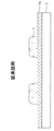
以下、図1a乃至図1cは、フォトリソグラフィー工程及びエッチング工程を用いて薄膜パターンを形成する技術を示す順序図である。 Hereinafter, FIGS. 1A to 1C are flowcharts showing a technique for forming a thin film pattern using a photolithography process and an etching process.
まず、図1aに示すように、平板表示素子用基板2上にスパッタリングなどの蒸着方法により金属層4aが形成される。以後、フォトレジスト塗布、露光及び現像工程を含むフォトリソグラフィー工程が行われることによって、図1bに示すように、フォトレジストパターン5が形成される。このフォトレジストパターン5をマスクといて用いたエッチング工程が行われることによって、図1cに示すように、第1薄膜パターン4が形成される。
First, as shown in FIG. 1a, a
このようなフォトリソグラフィー工程により多数の薄膜パターンが積層され、各々の薄膜パターンの電気的な接触などにより、薄膜パターンが必要によって電気的に連結されたり電気的に絶縁されたりする。ここで、各々の金属薄膜パターンを電気的に絶縁させようとする場合、絶縁膜が用いられる。 A large number of thin film patterns are stacked by such a photolithography process, and the thin film patterns are electrically connected or electrically insulated as necessary by electrical contact of the thin film patterns. Here, in order to electrically insulate each metal thin film pattern, an insulating film is used.
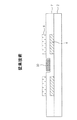
図2を参照すれば、図1a乃至図1cにより形成された第1薄膜パターン4と電気的に分離される第2薄膜パターン8を形成しようとする場合、絶縁膜6を形成した後、前述したフォトリソグラフィー工程及びエッチング工程により第2薄膜パターン8を形成する。
Referring to FIG. 2, when forming the second
ここで、絶縁膜6には、窒化シリコン(SiNx)などの無機絶縁物質がPECVDなどの蒸着方法により少なくとも2回以上蒸着されることにより形成される。
Here, the
ここで、無機絶縁物質からなる絶縁膜6は、下部に位置する第1薄膜パターン4により形成される段差をそのまま維持するようにすることで、基板2上の平坦化度を低下させる短所がある。このような無機物質の絶縁膜6の短所を補完するために、図3に示すように、有機物質で形成された有機絶縁膜7を形成する技術が提案された。有機絶縁膜7は、無機絶縁膜6と異に、PECVDなどの蒸着方法でないスピンコーティングまたはスピンリスコーティングなどのコーティング方法により有機物が塗布された後、乾燥されることにより形成される。このような有機絶縁膜7は、無機絶縁膜6と異に、第1薄膜パターン4による段差が除去できることになる。また、有機絶縁膜8は2回の蒸着工程による無機絶縁膜6より製造工程が単純で、かつ、費用が低廉である。
Here, the
一方、金属薄膜パターン(または、金属)と金属薄膜パターン(または、金属)が絶縁物質により絶縁され、各々の金属薄膜パターンに電流または電圧が供給されれば、金属薄膜パターン間に寄生キャパシタが形成される。 On the other hand, if the metal thin film pattern (or metal) and the metal thin film pattern (or metal) are insulated by an insulating material and a current or voltage is supplied to each metal thin film pattern, a parasitic capacitor is formed between the metal thin film patterns. Is done.
即ち、第1薄膜パターン4と第2薄膜パターン6に、電流または電圧が供給されれば、第1薄膜パターン4と第2薄膜パターン6との間に第1寄生キャパシタAが形成される。また、第3薄膜パターン10が形成される場合は、第1薄膜パターン4と第3薄膜パターン10との間に第2寄生キャパシタBが形成される。
That is, when a current or voltage is supplied to the first
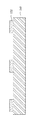
このような寄生キャパシタA、Bは、使用者の必要によって、その容量を大きく形成したり小さく形成する必要がある。このために、図4に示すように、有機絶縁膜7の厚さを調節する必要がある。
Such parasitic capacitors A and B need to have a large or small capacitance depending on the needs of the user. Therefore, it is necessary to adjust the thickness of the organic
![]()
![]()
即ち、キャパシタは数式1のように、電極間の距離に反比例するので、有機絶縁膜7の厚さを調節することによって、寄生キャパシタの容量が調節できることになる。
That is, since the capacitor is inversely proportional to the distance between the electrodes as expressed by
しかしながら、図4に示すように、有機絶縁膜7の段差を形成しようとする場合は、マスクを用いたフォトリソグラフィー工程が必要となる。
However, as shown in FIG. 4, when a step in the organic
即ち、有機絶縁物質を塗布した後、ハーフトーンマスクなどを用いて部分的に有機絶縁物質を露光した後、現像することで、段差を有する有機絶縁膜7が形成できることになる。
That is, after applying the organic insulating material, the organic insulating material is partially exposed using a halftone mask and then developed, whereby the organic
しかしながら、このようなマスクを用いたフォトリソグラフィー工程は、露光、現像工程とマスク製作費用などが追加されることによって、段差を有する有機絶縁膜7を形成する場合、製造工程が複雑になり、費用が顕著に増加する問題がある。
However, in the photolithography process using such a mask, when the organic
本発明は、フォト工程を使用しないで、段差を有する有機物パターンを形成することによって、キャパシタの容量が調節できる薄膜パターンの製造方法及びこれを用いる平板表示素子の製造方法を提供することをその目的とする。 An object of the present invention is to provide a method of manufacturing a thin film pattern in which the capacitance of a capacitor can be adjusted by forming an organic pattern having a step without using a photo process, and a method of manufacturing a flat panel display device using the same. And
前記目的を達成するために、本発明の第1の側面としての薄膜パターンの製造方法は、基板上に導電性第1薄膜パターンを形成するステップと、第2薄膜パターンが形成されたマスターモールドを形成するステップと、第2薄膜パターンが形成されたマスターモールド上に有機物を塗布するステップと、第1薄膜パターン及び基板の表面が有機物と接触するように基板と前記マスターモールドとを合着するステップと、有機物を硬化するステップと、基板とマスターモールドを分離して第1薄膜パターンが形成された基板上に第2薄膜パターンにより段差が形成された有機薄膜パターンを形成するステップと、を含む。 In order to achieve the above object, a thin film pattern manufacturing method according to a first aspect of the present invention includes a step of forming a conductive first thin film pattern on a substrate, and a master mold on which the second thin film pattern is formed. A step of forming, a step of applying an organic substance on the master mold on which the second thin film pattern is formed, and a step of bonding the substrate and the master mold so that the first thin film pattern and the surface of the substrate are in contact with the organic substance. And a step of curing the organic substance, and a step of separating the substrate and the master mold and forming an organic thin film pattern in which a step is formed by the second thin film pattern on the substrate on which the first thin film pattern is formed.
さらに、第2薄膜パターンが形成されたマスターモールド上に有機物を塗布した後、有機物の表面に粘着剤を形成するステップを含んでもよい。 Furthermore, after apply | coating organic substance on the master mold in which the 2nd thin film pattern was formed, you may include the step which forms an adhesive on the surface of organic substance.
本発明の第2の側面としての平板表示素子の製造方法は、基板上に、ゲートライン、ゲートラインと接触するゲート電極を含むゲートパターンを形成するステップと、所定の薄膜パターンを具備するマスターモールドを設けるステップと、薄膜パターンが形成されたマスターモールド上に有機物を塗布するステップと、ゲートパターン及び基板の表面が有機物と接触すると共に、薄膜パターンとゲートラインが対向するように基板とマスターモールドとを合着するステップと、有機物を硬化するステップと、基板及びマスターモールドを分離して基板上にゲートラインと重畳される領域で相対的に小さな厚さを有する有機ゲート絶縁膜を形成するステップと、を含む。 A flat panel display device manufacturing method according to a second aspect of the present invention includes a step of forming a gate pattern including a gate line and a gate electrode in contact with the gate line on a substrate, and a master mold having a predetermined thin film pattern. A substrate and a master mold so that the gate pattern and the surface of the substrate are in contact with the organic material, and the thin film pattern and the gate line are opposed to each other. Bonding the organic material, curing the organic material, separating the substrate and the master mold, and forming an organic gate insulating film having a relatively small thickness in a region overlapping the gate line on the substrate; ,including.
またさらに、有機ゲート絶縁膜上に半導体パターンを形成するステップと、半導体パターン上にソース電極及びドレーン電極、ゲートラインと交差するデータラインを形成するステップと、ドレーン電極を露出させる接触ホールを有する保護膜を形成するステップと、接触ホールを通じてドレーン電極と接触し、相対的に低い厚さを有する有機ゲート絶縁膜を挟んで前記ゲートラインとストレージキャパシタをなす画素電極を形成するステップと、を含む。 Further, a step of forming a semiconductor pattern on the organic gate insulating film, a step of forming a data line intersecting the source electrode and the drain electrode and the gate line on the semiconductor pattern, and a protection having a contact hole exposing the drain electrode. Forming a film, and forming a pixel electrode which is in contact with the drain electrode through the contact hole and forms a storage capacitor with the gate line sandwiching the organic gate insulating film having a relatively low thickness.
上記第1及び第2の側面において、有機物の表面エネルギー及びマスターモールドの表面エネルギーより大きいことを特徴とする。 Said 1st and 2nd side surface is larger than the surface energy of organic substance, and the surface energy of a master mold, It is characterized by the above-mentioned.
本発明の第3の側面は、上記第1の側面によって製造された有機薄膜パターンを有する装置である。 The 3rd side surface of this invention is an apparatus which has the organic thin film pattern manufactured by the said 1st side surface.
本発明の第4の側面は、薄膜パターンを有する装置であって、基板、基板上に形成された導電性薄膜パターン、並びに基板及び導電性薄膜パターン上に接合された有機物からなる有機薄膜パターンであって外側表面に段差を有する有機薄膜パターンを含み、有機薄膜パターンが、段差に対応する表面を有するマスターモールドから分離され移されたものであり、基板の表面エネルギーが有機物及びマスターモールドの表面エネルギーよりも大きい装置である。 A fourth aspect of the present invention is an apparatus having a thin film pattern, which is a substrate, a conductive thin film pattern formed on the substrate, and an organic thin film pattern made of an organic substance bonded on the substrate and the conductive thin film pattern. Including an organic thin film pattern having a step on the outer surface, the organic thin film pattern is separated and transferred from a master mold having a surface corresponding to the step, and the surface energy of the substrate is the surface energy of the organic matter and the master mold. Larger device.
上記第1から第4の側面において、各構成要素の詳細は以下の通りである。 In the first to fourth aspects, details of each component are as follows.
基板の表面は、O2プラズマにより親水化処理される。 The surface of the substrate is hydrophilized with O 2 plasma.
基板の表面エネルギーは、70〜100mN/m程度である。 The surface energy of the substrate is about 70 to 100 mN / m.
マスターモールド上に塗布される有機物は、液状前駆体のポリマーであるレジンであって、アクリレート系モノマーとホスフィンオキサイド及びケトンのうち、少なくともいずれか1つの光開始剤を含む。 The organic material applied on the master mold is a resin that is a polymer of a liquid precursor, and includes at least one photoinitiator of an acrylate monomer, a phosphine oxide, and a ketone.
また、有機物はトリデカフルオロ及びテトラヒドロオクチル・トリクロロシランのうちの少なくとも1つを含むプライマからなる。 The organic substance is composed of a primer containing at least one of tridecafluoro and tetrahydrooctyl / trichlorosilane.
有機物内でアクリレート系モノマーの含有量は90〜98%程度であり、ホスフィンオキサイド及びケトンのうち、少なくともいずれか1つの含有量は2〜10%程度である。 In the organic substance, the content of the acrylate monomer is about 90 to 98%, and the content of at least one of phosphine oxide and ketone is about 2 to 10%.
有機物の表面エネルギーは、20〜45mN/m程度である。 The surface energy of the organic substance is about 20 to 45 mN / m.
また、有機物の好適な粘度は1〜50cPである。 Moreover, the suitable viscosity of organic substance is 1-50 cP.
マスターモールドの表面は、CF4プラズマまたはSF6プラズマのうち、いずれか1つにより疎水化処理される。 The surface of the master mold is hydrophobized with either one of CF 4 plasma or SF 6 plasma.
マスターモールドの表面エネルギーは、15〜40mN/m程度である。 The surface energy of the master mold is about 15 to 40 mN / m.
有機物のアクリレート系モノマーは親水性である。 The organic acrylate monomer is hydrophilic.
本発明に係る平板表示素子の製造方法は、フォト工程でない別途のマスターモールド及び物質間の表面エネルギーを用いて段差を有する有機物パターンを形成することができる。これによって、キャパシタの容量が調節できることになる。 The method for manufacturing a flat panel display device according to the present invention can form an organic pattern having a step by using a separate master mold that is not a photo process and surface energy between materials. As a result, the capacitance of the capacitor can be adjusted.
また、このような段差付けた有機物パターンは、薄膜トランジスタアレイ基板でストレージキャパシタに用いられるようになることで、ストレージキャパシタの容量が最大化でき、画質を改善させることができることになる。 Further, such a stepped organic material pattern can be used for a storage capacitor in a thin film transistor array substrate, whereby the capacity of the storage capacitor can be maximized and the image quality can be improved.
以下、本発明の好ましい実施形態を図5a乃至図10eを参照しつつ詳細に説明する。 Hereinafter, a preferred embodiment of the present invention will be described in detail with reference to FIGS. 5a to 10e.
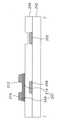
図5a乃至図5fは、本発明に係る薄膜パターンの製造方法、特に、段差を有する有機物パターンの形成方法を示す図である。 5a to 5f are views showing a method of manufacturing a thin film pattern according to the present invention, particularly a method of forming an organic pattern having a step.
まず、従来の図1a乃至図1cに説明したフォトリソグラフィー工程及びエッチング工程と同一な工程により、図5aに示すように、基板102上に第1薄膜パターン104が形成される。
First, as shown in FIG. 5a, a first
以後、図5bに示すように、第1薄膜パターン104が形成された基板102と別途に最終形成しようとする有機物パターンで相対的に低い高さを有する領域と対応する領域に第2薄膜パターン152が位置するマスターモールド150を設ける。
Thereafter, as shown in FIG. 5b, the second
ここで、マスターモールド150はガラスで形成されることができる。
Here, the
以後、第1薄膜パターン104が形成された基板102に形成しようとする有機物パターンのための有機物質107aをマスターモールド150に塗布する。ここで、有機物質107aは光硬化性または熱硬化性有機物が用いられる。以後、図5cに示すように、有機物質107aと第1薄膜パターン104とが互いに対向する方向に基板102がマスターモールド150上に整列される。
Thereafter, an
以後、図5dに示すように、第1薄膜パターン104が形成された基板102を有機物質107aに接触させる。
Thereafter, as shown in FIG. 5d, the
以後、紫外線(UV)を用いた光硬化または熱硬化(サーマルキュアリング)工程により有機物質107aを硬化させる。以後、基板102をマスターモールド150と分離させる。この際、図5eに示すように、有機物質107aが基板102上に付着されることになる。これによって、基板102上に段差を有する有機物パターン、即ち、段差を有する有機薄膜パターン107が形成できることになる。
Thereafter, the
以後、フォトリソグラフィー工程など、その他の工程などが行われることによって、図5fに示すように、有機絶縁膜107上に第2または第3薄膜パターン108、110が形成される。
Thereafter, by performing other processes such as a photolithography process, the second or third
前述したように、本発明に係る段差を有する有機薄膜パターンは、フォト工程でないマスターモールドという別途の装備を用いると共に、後述する表面エネルギーの差を用いて形成されることができる。 As described above, the organic thin film pattern having a step according to the present invention can be formed by using a separate equipment called a master mold that is not a photo process and using a difference in surface energy described later.
以下、図5a乃至図5fに図示された段差を有する有機薄膜パターン107が形成できる技術的な原理とそれによる技術具現が可能な条件について具体的に説明する。
Hereinafter, a technical principle capable of forming the organic
まず、図5dにおいて、有機物質107aがマスターモールド150から分離されて、第1薄膜パターン104が形成された基板102に付着されるには、基板102の表面エネルギー(γ1)は有機物質107aの表面エネルギー(γ2)及びマスターモールド150の表面エネルギー(γ3)より大きくなければならない。(γ1>γ2、γ1>γ3)
First, in FIG. 5d, in order for the
ここで、表面エネルギー(γ)は、ある物質が空気と界面をなすときに要るエネルギーをいう。表面エネルギー(γ)の高い物質は空気と界面をなすときのエネルギーが高いため、空気と界面をなし難く、前記表面エネルギー(γ)の高い物質は、表面エネルギー(γ)の低い物質と界面をなし易い。即ち、表面エネルギー(γ)の低い流動性物質が表面エネルギー(γ)の高い固状物質の表面に蒸着されると、前記固状物質の表面上で前記流動性物質が広く広まることになる。前記流動性物質が前記固状物質より空気と界面をなそうとする特性が更に強く、前記固状物質は空気より前記流動性物質と界面をなそうとする特性が更に強いためである。表面エネルギー(γ3)を有する第1の固状物質上に蒸着された樹脂物質(その表面エネルギーはγ2)が表面エネルギー(γ1)を有する第2の固状物質と接触すると(ここで、γ1>γ2、γ1>γ3)、前記樹脂物質が前記第2の固状物質に移動されるが、これは前記第1の固状物質が前記第2の固状物質より空気と界面をなし易く、前記樹脂物質が前記第1固状物質より前記第2の固状物質と界面をなし易いためである。従って、本発明の方法においては、基板102と、マスターモールド150上に形成された有機物質107aとを接合する際に両者に機械的な圧力をかける必要はない。即ち、上述したように、必要なのは双方を接触させることだけである。
Here, the surface energy (γ) refers to energy required when a certain substance forms an interface with air. A substance with a high surface energy (γ) has a high energy when it makes an interface with air, so it is difficult to form an interface with air. A substance with a high surface energy (γ) has an interface with a substance with a low surface energy (γ). Easy to do. That is, when a fluid substance having a low surface energy (γ) is deposited on the surface of a solid substance having a high surface energy (γ), the fluid substance spreads widely on the surface of the solid substance. This is because the fluid substance has a stronger property to make an interface with air than the solid substance, and the solid substance has a stronger characteristic to make an interface with the fluid substance than air. When the resin material (the surface energy is γ2) deposited on the first solid material having the surface energy (γ3) comes into contact with the second solid material having the surface energy (γ1) (where γ1> γ2, γ1> γ3), the resin substance is transferred to the second solid substance, which is more likely to form an interface with the air than the second solid substance. This is because the resin substance can easily form an interface with the second solid substance than the first solid substance. Therefore, in the method of the present invention, when the
前述した特性を示す表面エネルギー(γ)の差を用いて表面エネルギー(γ)の低いマスターモールド150から有機物質107aが容易に分離できることになる。これと反対に、相対的に表面エネルギー(γ)の高い基板102は相対的に表面エネルギー(γ)の小さい有機物質107aと界面をなそうとする性質が強くなる。即ち、有機物質107aと界面をなそうとする性質が強いという意味は、互いに粘着しようとする粘着力が強くなることを意味する。
The
したがって、本発明は、このような表面エネルギー(γ)の性質を用いてフォト工程でない成型工程を用いて段差を有する有機薄膜パターンが形成できることになる。 Therefore, according to the present invention, an organic thin film pattern having a step can be formed using a molding process that is not a photo process using such a property of surface energy (γ).
このために、基板102の表面エネルギーは、70mN/m以上でなければならない(ここで、mN/m単位は、mJ/m2に換算して表現することもできる)。一般に、ガラス(glass)基板の場合、表面エネルギーは100mN/m以上の値を有する。しかしながら、もし40mN/m以下の表面エネルギーを有する基板を用いる場合、O2プラズマ処理などを通じて表面エネルギーが70mN/m以上になるようにする。即ち、親水性の程度は、即ち表面エネルギーと比例関係を有することになることにより、O2プラズマ処理を通じて基板102を親水化させると共に、70mN/m以上の表面エネルギーを有することになる。
For this reason, the surface energy of the
マスターモールド150で基板を用いる場合、表面エネルギーは、第1薄膜パターン104が形成された基板102の表面エネルギーより相対的に小さくなければならない。このために、マスターモールド用基板150はふっ素(F)を含有するCF4及びSF6プラズマ処理を通じて表面を疎水化させることによって、表面エネルギーを15〜40mN/m程度に下げられることになる。
When a substrate is used in the
有機物質107aは、液状前駆体のポリマーであるレジン(resin)でなければならなくて、その表面エネルギーは、第1薄膜パターン104が形成された基板102の表面エネルギーより相対的に小さくなければならない。ここで、液状高分子前駆体形態のレジンは、アクリレート系モノマーにホスフィンオキサイド及びケトンのうち、少なくともいずれか1つの光開始剤が添加されることにより製造される。より具体的には、アクリレート系モノマーが90〜98%程度含まれており、ホスフィンオキサイド及びケトンのうち、少なくともいずれか1つが2〜10%程度含まれている。ここで、有機物質は好ましくはトリデカフルオロ及びテトラヒドロオクチル・トリクロロシランのうちの少なくとも1つを含むプライマからなる。そして、有機物質の好適な粘度は1〜50cPである。
The
このような液状前駆体のポリマーであるレジンは、20〜44mN/m程度の表面エネルギー値を有する。 The resin, which is a polymer of such a liquid precursor, has a surface energy value of about 20 to 44 mN / m.
これによって、基板の表面エネルギー(γ1)、有機物質の表面エネルギー(γ2)、マスターモールド150の表面エネルギー(γ3)は、γ1>γ2、γ1>γ3の関係を有することになる。
Thus, the surface energy (γ1) of the substrate, the surface energy (γ2) of the organic substance, and the surface energy (γ3) of the
その結果、図5dにおいて、表面エネルギーが相対的に最も大きい基板102と有機物質107aとの粘着力が増加し、有機物質107aとマスターモールド150との間の粘着力は低下することによって、有機物質107aが第1薄膜パターン104が形成された基板102に付着できることになる。
As a result, in FIG. 5d, the adhesive force between the
前述した表面エネルギーの以外に界面面積に従う条件が追加されることができる。 In addition to the surface energy described above, a condition according to the interface area can be added.
即ち、マスターモールド150上の有機物質107aが基板102上に伝えられるようにするためには、数式2を満足しなければならない。
That is, in order for the
[数式2]
A23(γ2+γ3−γ23)<A12(γ2+γ1―γ12)
(A23:有機物質とマスターモールド用基板との接触面積、A12:有機物質と基板との接触面積、γ23:有機物質とマスターモールド用基板間の相互表面エネルギー、γ12:基板と有機物質との間の相互表面エネルギー)
[Formula 2]
A23 (γ2 + γ3-γ23) <A12 (γ2 + γ1-γ12)
(A23: contact area between organic substance and master mold substrate, A12: contact area between organic substance and substrate, γ23: mutual surface energy between organic substance and master mold substrate, γ12: between substrate and organic substance Mutual surface energy)
ここで、A23はマスターモールド用基板150上に形成された第2薄膜パターン152の個数が多くなれば、それほど接触面積は広くなることになり、A12はまた基板102上の第1薄膜パターン104の個数が多くなれば、それほど接触面積は広くなることになる。結果的に、A23及びA12は、各々の薄膜パターンの個数によって変わることになる。
Here, if the number of the second
したがって、前記数式2の満足の可否は、A23及びA12値により変わることができるので、次のように場合を分けて考察する。
Therefore, whether or not the
まず、A23≦A12、または、A23/A12=1.5の場合には、γ23を増加させ、γ12を減少する方向に設計しなければならない。ここで、γ23を増加させるという意味は、有機物質107aとマスターモールド用基板150との反撥力を増加させるのであり、γ12を減少させるという意味は、有機物質107aとマスターモールド用基板150との粘着力を増加させるのである。ここで、基板102は親水性であり、マスターモールド150は疎水性であるから、親水性有機物質107aを用いる場合、γ23は増加され、γ12は減少できることになる。
First, in the case of A23 ≦ A12 or A23 / A12 = 1.5, it is necessary to design γ23 to increase and γ12 to decrease. Here, the meaning of increasing γ23 is to increase the repulsive force between the
結果的に、A23=A12、または、A23/A12=1.5の場合には、有機物質107aの親水性の程度を調節することによって、数式2を満足させることになる。親水性有機物質107aは、親水性アクリレートモノマーを用いることで、有機物質107aを親水化させることになる。または、O2プラズマ処理をすることで、有機物質107aの表面を親水化することもできる。
As a result, when A23 = A12 or A23 / A12 = 1.5,
次に、A23/A12>1.5の場合には数式を満足することが多少困難であり得る。この場合は、有機物質107aの表面にスプレーまたはコーティング方式などを用いてプライマなどの粘着物質を形成させる。これによって、有機物質107aは、第1薄膜パターン104が形成された基板102上に接着させることができることになる。
Next, when A23 / A12> 1.5, it may be somewhat difficult to satisfy the mathematical formula. In this case, an adhesive material such as a primer is formed on the surface of the
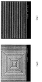
その結果、第1薄膜パターン104が形成された基板102上に段差を有する有機薄膜パターン107が形成できることになる。図11(a)及び(b)はテスト基板の上面からの拡大写真である。有機物質107上の段差は色の違い(濃淡)によって表されている。図11(a)及び(b)は、段差が渦巻状及び縞状に形成された例をそれぞれ示している。
As a result, an organic
以下、図6乃至図10eを参照して、詳述した方式により形成された段差を有する有機薄膜パターンの製造方法が液晶表示パネルの薄膜トランジスタアレイ基板に利用できることを説明する。 Hereinafter, it will be described with reference to FIGS. 6 to 10e that a method of manufacturing an organic thin film pattern having a step formed by the detailed method can be used for a thin film transistor array substrate of a liquid crystal display panel.
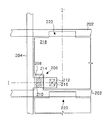
まず、図6は通常の薄膜トランジスタアレイ基板を示す平面図であり、図7は図1に図示された薄膜トランジスタアレイ基板をI−I’線に沿って切断して示す断面図である。 First, FIG. 6 is a plan view showing a normal thin film transistor array substrate, and FIG. 7 is a sectional view showing the thin film transistor array substrate shown in FIG. 1 cut along the line I-I '.
図6及び図7に図示された薄膜トランジスタアレイ基板は、下部基板242の上に有機ゲート絶縁膜244を挟んで交差するように形成されたゲートライン202及びデータライン204と、その交差部毎に形成された薄膜トランジスタ(Thin Film Transistor;以下、“TFT”という)206と、その交差構造で設けられたセル領域に形成された画素電極218とを具備する。そして、TFTアレイ基板は画素電極218と以前段のゲートライン202の重畳部に形成されたストレージキャパシタ220を具備する。
The thin film transistor array substrate shown in FIGS. 6 and 7 is formed at each intersection of the
TFT206は、ゲートライン202に接続されたゲート電極208と、データライン204に接続されたソース電極210と、画素電極218に接続されたドレーン電極212と、ゲート電極208と重畳され、ソース電極210とドレーン電極212との間にチャンネルを形成する活性層214とを具備する。活性層214は、データライン204、ソース電極210及びドレーン電極212と重畳されるように形成され、ソース電極210とドレーン電極212との間のチャンネル部を更に含む。活性層214の上にはデータライン204、ソース電極210及びドレーン電極212とオーミック接触のためのオーミック接触層248が更に形成される。ここで、活性層214及びオーミック接触層248を半導体パターン247と命名する。
The
このようなTFT206は、ゲートライン202に供給されるゲート信号に応答してデータライン204に供給される画素電圧信号が画素電極218に充電されて維持されるようにする。
Such a
画素電極218は保護膜250を貫通する接触ホール216を通じてTFT206のドレーン電極212と接続される。画素電極218は、充電された画素電圧により図示しない上部基板に形成される共通電極と電位差を発生させることになる。この電位差によりTFTアレイ基板とカラーフィルターアレイ基板との間に位置する液晶が誘電異方性により回転することになり、図示しない光源から画素電極218を経由して入射される光を上部基板側に透過させることになる。
The
ストレージキャパシタ220は、前段ゲートライン202と画素電極218により形成される。ゲートライン202と画素電極218との間には有機ゲート絶縁膜244及び保護膜250が位置することになる。このようなストレージキャパシタ220は、画素電極218に充電された画素電圧が次の画素電圧が充電されるまで維持されるように助けを与えることになる。
The
このようなTFTアレイ基板は、TFT106のゲート電極208に、図8に示すように、ゲート電圧(Vg)が供給され、ソース電極210にはデータ電圧(Vd)が供給される。TFT206のゲート電極208にTFT206の臨界電圧以上のゲート電圧(Vg)が印加されればソース電極210とドレーン電極212との間にチャンネルが形成されながらデータ電圧(Vd)がTFTのソース電極210とドレーン電極212を経由して液晶セル(Clc)とストレージキャパシタ220(Cst)に充電される。
In such a TFT array substrate, a gate voltage (Vg) is supplied to the
ここで、データ電圧(Vd)と液晶セル(Clc)に充電される電圧(Vlc)の差であるフィードスルー電圧(Feed Through Voltage;△Vp)は下記の数式3と定義される。 Here, a feed through voltage (ΔVp), which is a difference between the data voltage (Vd) and the voltage (Vlc) charged in the liquid crystal cell (Clc), is defined as the following Equation 3.
![]()
![]()
ここで、CgdはTFTのゲート電極とドレーン電極との間に形成される寄生キャパシタであり、△VgはVgh電圧とVgl電圧との電圧の差である。 Here, Cgd is a parasitic capacitor formed between the gate electrode and the drain electrode of the TFT, and ΔVg is a voltage difference between the Vgh voltage and the Vgl voltage.
このようなフィードスルー電圧(△Vp)は、フリッカーなどの残像を表れるようにする等、画質低下の要因となっている。これによって、数式3によりフィードスルー電圧(△Vp)を最小化するために、ストレージキャパシタ220の容量(Cst)を最大化することによって、画質低下を減少させることができることになる。
Such a feedthrough voltage (ΔVp) is a factor of image quality deterioration, such as causing an afterimage such as flicker. Accordingly, in order to minimize the feedthrough voltage (ΔVp) according to Equation 3, the image quality degradation can be reduced by maximizing the capacity (Cst) of the
ここで、ストレージキャパシタ220容量(Cst)は数式1により電極面積Aに比例し、電極間の長さに反比例する。この際、ストレージキャパシタ220の容量(Cst)を高めるために電極の面積を広げることになれば開口率が減少する問題がある。
Here, the capacity (Cst) of the
結局、面積は固定させ、電極間の長さを小さくすることで、ストレージキャパシタ220の容量(Cst)が最大化できることになる。
Eventually, the capacitance (Cst) of the
ここで、本願発明で提案された段差を有する有機物パターン形成方法を用いて、図9に示すように、ストレージキャパシタ220で段差を有する有機ゲート絶縁膜244を形成する。これによって、ストレージキャパシタ220をなす画素電極218とゲートライン102との間の距離を狭められることになることで、ストレージキャパシタ220の容量(Cst)が最大化できることになる。
Here, using the organic pattern forming method having a step proposed in the present invention, an organic
その結果、フィードスルー電圧(△Vp)が最小化することによって、画質低下を減少させることができることになる。 As a result, the feedthrough voltage (ΔVp) is minimized, thereby reducing image quality degradation.
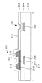
以下、図10a乃至図10dを用いて、図7に図示された薄膜トランジスタアレイ基板の形成方法を説明すれば、次の通りである。 Hereinafter, a method for forming the thin film transistor array substrate illustrated in FIG. 7 will be described with reference to FIGS. 10A to 10D.
まず、下部基板242上にスパッタリング方法などの蒸着方法によりゲート金属層が形成された後、フォトリソグラフィー工程とエッチング工程でゲート金属層がパターニングされることにより、図10aに示すように、ゲートライン202、ゲート電極208を含むゲートパターンが形成される。
First, after a gate metal layer is formed on the
以後、図5a乃至図5fに図示された薄膜パターンの形成方法を用いて、図10bに示すように、ゲートライン202と重畳される領域で相対的に低い厚さを有する段差付けた有機ゲート絶縁膜244を形成する。即ち、図10aでのゲートライン202、ゲート電極208は、図5aでの第1薄膜パターン104と対応し、図5fに図示された有機ゲート絶縁膜244は段差付けた有機薄膜パターン107と対応することになる。これを除いては、有機ゲート絶縁膜244の形成方法は、図5a乃至図5fと同一な方式により形成されるので、以下の詳細な説明は省略する。
Thereafter, using the thin film pattern forming method shown in FIGS. 5a to 5f, the stepped organic gate insulation having a relatively low thickness in the region overlapping the
有機ゲート絶縁膜244が形成された下部基板242上に非晶質シリコン層、n+非晶質シリコン層、そしてソース/ドレーン金属層が順次に形成される。
An amorphous silicon layer, an n + amorphous silicon layer, and a source / drain metal layer are sequentially formed on the
ソース/ドレーン金属層の上に回折マスクを用いたフォトリソグラフィー工程及びエッチング工程などを用いて、図10cに示すように、データライン(図示していない)、ソース電極210、ドレーン電極212を含むソース/ドレーンパターンと、ソースドレーンパターンの下部にオーミック接触層248と活性層214を含む半導体パターン247が形成される。
A source including a data line (not shown), a
一方、半導体パターン247は、別途のマスク工程を用いてソース/ドレーンパターンとは別に形成されることができる。
Meanwhile, the
ソース/ドレーンパターンが形成された有機ゲート絶縁膜244上にPECVDなどの蒸着方法により保護膜250が全面形成された後、フォトリソグラフィー工程とエッチング工程によりパターニングされることによって、図10dに示すように、接触ホール216が形成される。接触ホール216は保護膜250を貫通してドレーン電極212が露出されるように形成される。
As shown in FIG. 10d, a
保護膜250上にスパッタリングなどの蒸着方法により透明電極物質が全面蒸着された後、フォトリソグラフィー工程とエッチング工程を通じて透明電極物質がパターニングされることにより、図10eに示すように、画素電極218が形成される。画素電極218は接触ホール216を通じてドレーン電極212と電気的に接続される。また、画素電極218は、有機ゲート絶縁膜244のうち、相対的に低い厚さを有する領域及び保護膜250を挟んで前段ゲートライン202と重畳されるように形成されることによって、ストレージキャパシタ220を構成する。
After the transparent electrode material is deposited on the entire surface of the
一方、本発明に係る薄膜パターンの製造方法は、液晶表示素子(LCD)に限るのでなく、電界放出表示素子(FED)、プラズマディスプレイパネル(PDP)及び電界発光素子(EL)等、いかなる表示素子の工程に用いられることができる。 On the other hand, the thin film pattern manufacturing method according to the present invention is not limited to a liquid crystal display element (LCD), but any display element such as a field emission display element (FED), a plasma display panel (PDP), and an electroluminescence element (EL). It can be used in the process.
2、102 基板
4、104 第1薄膜パターン
6 絶縁膜
7 有機絶縁膜
8、152 第2薄膜パターン
10、108、110 第3薄膜パターン
5 フォトレジストパターン
150 マスターモールド用基板
107a 有機物質
107 有機薄膜パターン
20、220 ストレージキャパシタ
202 ゲートライン
244 有機ゲート絶縁膜
250 保護膜
208 ゲート電極
206 薄膜トランジスタ
218 画素電極
2, 102
Claims (37)
第2薄膜パターンが形成されたマスターモールドを設けるステップ、
前記第2薄膜パターンが形成されたマスターモールド上に有機物を塗布するステップ、
前記第1薄膜パターン及び前記基板の表面が前記有機物と接触するように前記基板と前記マスターモールドとを合着するステップ、
前記有機物を硬化するステップ、及び
前記基板とマスターモールドを分離して、前記第1薄膜パターンが形成された基板上に前記第2薄膜パターンにより段差を有することになる有機薄膜パターンを形成するステップ、
を含むことを特徴とする薄膜パターンの製造方法。 Forming a conductive first thin film pattern on a substrate;
Providing a master mold having the second thin film pattern formed thereon;
Applying an organic material on the master mold on which the second thin film pattern is formed;
Bonding the substrate and the master mold so that the surface of the first thin film pattern and the substrate is in contact with the organic matter;
Curing the organic material, and separating the substrate and the master mold, and forming an organic thin film pattern having a step by the second thin film pattern on the substrate on which the first thin film pattern is formed,
The manufacturing method of the thin film pattern characterized by including.
所定の薄膜パターンを具備するマスターモールドを設けるステップと、
前記薄膜パターンが形成されたマスターモールド上に有機物を塗布するステップと、
前記ゲートパターン及び前記基板の表面が前記有機物と接触すると共に、前記薄膜パターンと前記ゲートラインが対向するように前記基板と前記マスターモールドとを合着するステップと、
前記有機物を硬化するステップと、
前記基板及びマスターモールドを分離して前記基板上に前記ゲートラインと重畳される領域で相対的に小さな厚さを有する有機ゲート絶縁膜を形成するステップと、
を含むことを特徴とする平板表示素子の製造方法。 Forming a gate pattern including a gate line on the substrate and a gate electrode connected to the gate line;
Providing a master mold having a predetermined thin film pattern;
Applying an organic material on the master mold on which the thin film pattern is formed;
Bonding the substrate and the master mold so that the gate pattern and the surface of the substrate are in contact with the organic matter, and the thin film pattern and the gate line face each other;
Curing the organic matter;
Separating the substrate and the master mold and forming an organic gate insulating film having a relatively small thickness in a region overlapping the gate line on the substrate;
The manufacturing method of the flat panel display element characterized by the above-mentioned.
前記半導体パターン上にソース電極及びドレーン電極、前記ゲートラインと交差するデータラインを形成するステップ、
前記ドレーン電極を露出させる接触ホールを有する保護膜を形成するステップ、及び
前記接触ホールを通じて前記ドレーン電極と接触し、前記相対的に低い厚さを有する有機ゲート絶縁膜を挟んで前記ゲートラインとストレージキャパシタをなす画素電極を形成するステップ、
を含むことを特徴とする請求項14記載の平板表示素子の製造方法。 Forming a semiconductor pattern on the organic gate insulating film;
Forming a source electrode and a drain electrode on the semiconductor pattern, and a data line intersecting with the gate line;
Forming a protective film having a contact hole exposing the drain electrode; and contacting the drain electrode through the contact hole and sandwiching the organic gate insulating film having a relatively low thickness with the gate line and the storage Forming a pixel electrode forming a capacitor;
The method of manufacturing a flat panel display device according to claim 14, comprising:
基板、
該基板上に形成された導電性薄膜パターン、及び
該基板及び該導電性薄膜パターン上に接合された有機物からなる有機薄膜パターンであって、外側表面に段差を有する有機薄膜パターン
を含み、
該有機薄膜パターンが、該段差に対応する表面を有するマスターモールドから分離され移されたものであり、
該基板の表面エネルギーが該有機物及び該マスターモールドの表面エネルギーよりも大きいことを特徴とする装置。 An apparatus having a thin film pattern,
substrate,
A conductive thin film pattern formed on the substrate, and an organic thin film pattern made of an organic material bonded on the substrate and the conductive thin film pattern, the organic thin film pattern having a step on the outer surface,
The organic thin film pattern is separated and transferred from a master mold having a surface corresponding to the step,
The apparatus characterized in that the surface energy of the substrate is larger than the surface energy of the organic substance and the master mold.
Applications Claiming Priority (1)
| Application Number | Priority Date | Filing Date | Title |
|---|---|---|---|
| KR1020050129702A KR101157983B1 (en) | 2005-12-26 | 2005-12-26 | Method for Fabricating Thin Film Pattern and Method for Fabricating Flat Panel Display Device Using the same |
Publications (2)
| Publication Number | Publication Date |
|---|---|
| JP2007178995A true JP2007178995A (en) | 2007-07-12 |
| JP4584881B2 JP4584881B2 (en) | 2010-11-24 |
Family
ID=38192377
Family Applications (1)
| Application Number | Title | Priority Date | Filing Date |
|---|---|---|---|
| JP2006207623A Expired - Fee Related JP4584881B2 (en) | 2005-12-26 | 2006-07-31 | Thin film pattern manufacturing method and flat panel display device manufacturing method using the same |
Country Status (3)
| Country | Link |
|---|---|
| US (1) | US7544069B2 (en) |
| JP (1) | JP4584881B2 (en) |
| KR (1) | KR101157983B1 (en) |
Cited By (1)
| Publication number | Priority date | Publication date | Assignee | Title |
|---|---|---|---|---|
| JP2010074162A (en) * | 2008-09-19 | 2010-04-02 | Samsung Electronics Co Ltd | Method of forming pattern using nano imprint, and method of manufacturing mold for forming pattern |
Families Citing this family (6)
| Publication number | Priority date | Publication date | Assignee | Title |
|---|---|---|---|---|
| KR101432574B1 (en) * | 2008-04-30 | 2014-08-22 | 엘지디스플레이 주식회사 | Liquid crystal display device and method of fabricating the same |
| US8101519B2 (en) * | 2008-08-14 | 2012-01-24 | Samsung Electronics Co., Ltd. | Mold, manufacturing method of mold, method for forming patterns using mold, and display substrate and display device manufactured by using method for forming patterns |
| KR101015357B1 (en) | 2009-08-20 | 2011-02-16 | 삼성모바일디스플레이주식회사 | Master glass having a structure capable of preventing damage caused by static electricity |
| CN102214803B (en) * | 2011-05-20 | 2013-07-17 | 电子科技大学 | Packaging method of photoelectronic device |
| TWI595621B (en) | 2012-07-03 | 2017-08-11 | 元太科技工業股份有限公司 | Pixel structure and manufacturing method thereof |
| KR101963886B1 (en) * | 2017-03-16 | 2019-04-01 | 한국생산기술연구원 | Method for fabrication of micro electrodes using inkjet printing |
Citations (4)
| Publication number | Priority date | Publication date | Assignee | Title |
|---|---|---|---|---|
| JPH1073807A (en) * | 1996-04-15 | 1998-03-17 | Canon Inc | Wiring board, its production, liquid crystal element, its production and apparatus for production of wiring board |
| JP2003309344A (en) * | 2002-04-18 | 2003-10-31 | Dainippon Printing Co Ltd | Method of manufacturing basic material of conductive pattern |
| JP2004302495A (en) * | 2001-12-17 | 2004-10-28 | Seiko Epson Corp | Electro-optical device and electronic apparatus |
| JP2005093625A (en) * | 2003-09-17 | 2005-04-07 | Sony Corp | Thin-film semiconductor device, method for manufacturing the same and liquid crystal display |
Family Cites Families (8)
| Publication number | Priority date | Publication date | Assignee | Title |
|---|---|---|---|---|
| JPH10214974A (en) * | 1997-01-28 | 1998-08-11 | Semiconductor Energy Lab Co Ltd | Semiconductor device and its fabrication |
| US6955767B2 (en) * | 2001-03-22 | 2005-10-18 | Hewlett-Packard Development Company, Lp. | Scanning probe based lithographic alignment |
| DE10126860C2 (en) * | 2001-06-01 | 2003-05-28 | Siemens Ag | Organic field effect transistor, process for its manufacture and use for the construction of integrated circuits |
| KR20030075971A (en) * | 2002-03-22 | 2003-09-26 | 이홍희 | Method for fabricating thin film pattern for organic electronic devices |
| US7964439B2 (en) * | 2002-12-20 | 2011-06-21 | The Trustees Of Princeton University | Methods of fabricating devices by transfer of organic material |
| US20060108905A1 (en) * | 2004-11-25 | 2006-05-25 | Samsung Electronics Co., Ltd. | Mold for fabricating barrier rib and method of fabricating two-layered barrier rib using same |
| KR101050588B1 (en) * | 2004-11-30 | 2011-07-19 | 삼성전자주식회사 | Organic insulating film pattern formation method |
| KR101137865B1 (en) * | 2005-06-21 | 2012-04-20 | 엘지디스플레이 주식회사 | Fabricating method for thin flim transister substrate and thin flim transister substrate using the same |
-
2005
- 2005-12-26 KR KR1020050129702A patent/KR101157983B1/en active IP Right Grant
-
2006
- 2006-07-28 US US11/494,632 patent/US7544069B2/en not_active Expired - Fee Related
- 2006-07-31 JP JP2006207623A patent/JP4584881B2/en not_active Expired - Fee Related
Patent Citations (4)
| Publication number | Priority date | Publication date | Assignee | Title |
|---|---|---|---|---|
| JPH1073807A (en) * | 1996-04-15 | 1998-03-17 | Canon Inc | Wiring board, its production, liquid crystal element, its production and apparatus for production of wiring board |
| JP2004302495A (en) * | 2001-12-17 | 2004-10-28 | Seiko Epson Corp | Electro-optical device and electronic apparatus |
| JP2003309344A (en) * | 2002-04-18 | 2003-10-31 | Dainippon Printing Co Ltd | Method of manufacturing basic material of conductive pattern |
| JP2005093625A (en) * | 2003-09-17 | 2005-04-07 | Sony Corp | Thin-film semiconductor device, method for manufacturing the same and liquid crystal display |
Cited By (1)
| Publication number | Priority date | Publication date | Assignee | Title |
|---|---|---|---|---|
| JP2010074162A (en) * | 2008-09-19 | 2010-04-02 | Samsung Electronics Co Ltd | Method of forming pattern using nano imprint, and method of manufacturing mold for forming pattern |
Also Published As
| Publication number | Publication date |
|---|---|
| KR20070068035A (en) | 2007-06-29 |
| US7544069B2 (en) | 2009-06-09 |
| KR101157983B1 (en) | 2012-06-25 |
| US20070145004A1 (en) | 2007-06-28 |
| JP4584881B2 (en) | 2010-11-24 |
Similar Documents
| Publication | Publication Date | Title |
|---|---|---|
| JP4584881B2 (en) | Thin film pattern manufacturing method and flat panel display device manufacturing method using the same | |
| CA2178232C (en) | Lcd with bus lines overlapped by pixel electrodes and photo-imageable insulating layer therebetween | |
| US7710530B2 (en) | Color filter substrate and display apparatus using the same | |
| US6864133B2 (en) | Device, method of manufacturing device, electro-optic device, and electronic equipment | |
| TWI395026B (en) | Liquid crystal display device and method of fabricating the same | |
| WO2018014632A1 (en) | Display substrate, display panel, display apparatus, and method of fabricating display substrate and display panel | |
| KR20060099885A (en) | Flexible liquid crystal display and manufacturing method of the same | |
| JP2004078226A (en) | Substrate for liquid crystal display device, liquid crystal display device, and method for manufacturing the same | |
| US7826021B2 (en) | Substrate for liquid crystal display | |
| WO2017204114A1 (en) | Scanning antenna and method for manufacturing scanning antenna | |
| JP2008016806A (en) | Thin film transistor, method of manufacturing the same, and display element | |
| US8077267B2 (en) | TFT LCD array substrate wherein an air gap is formed between the insulating layer and the active layer and method of manufacturing thereof | |
| US20110019117A1 (en) | Tft-lcd array substrate and manufacturing method thereof | |
| US8115215B2 (en) | Array substrate and method for manufacturing the same | |
| US20020085149A1 (en) | Liquid crystal display device and method for manufacturing the same | |
| US7768012B2 (en) | LCD pixel array structure | |
| KR20090088575A (en) | Manufacturing method of thin film transistor substrate | |
| US9153487B2 (en) | Methods of forming wirings in electronic devices | |
| US7601552B2 (en) | Semiconductor structure of liquid crystal display and manufacturing method thereof | |
| JP2010191283A (en) | Method for manufacturing active element substrate, active element substrate, and active type display device | |
| US7920246B2 (en) | LCD device including semiconductor of nano material and method for fabricating the same | |
| JP2004165289A (en) | Active matrix substrate, manufacturing method therefor and display device | |
| CN113964086A (en) | Preparation method of display panel based on POA | |
| US20070243673A1 (en) | Thin-film transistor array for lcd and the method for manufacturing the same | |
| TW200523599A (en) | LCD device and manufacturing method thereof and transistor array substrate and manufacturing method thereof |
Legal Events
| Date | Code | Title | Description |
|---|---|---|---|
| A131 | Notification of reasons for refusal |
Free format text: JAPANESE INTERMEDIATE CODE: A131 Effective date: 20090715 |
|
| A521 | Written amendment |
Free format text: JAPANESE INTERMEDIATE CODE: A523 Effective date: 20091014 |
|
| A131 | Notification of reasons for refusal |
Free format text: JAPANESE INTERMEDIATE CODE: A131 Effective date: 20100215 |
|
| A521 | Written amendment |
Free format text: JAPANESE INTERMEDIATE CODE: A523 Effective date: 20100512 |
|
| TRDD | Decision of grant or rejection written | ||
| A01 | Written decision to grant a patent or to grant a registration (utility model) |
Free format text: JAPANESE INTERMEDIATE CODE: A01 Effective date: 20100811 |
|
| A01 | Written decision to grant a patent or to grant a registration (utility model) |
Free format text: JAPANESE INTERMEDIATE CODE: A01 |
|
| A61 | First payment of annual fees (during grant procedure) |
Free format text: JAPANESE INTERMEDIATE CODE: A61 Effective date: 20100902 |
|
| R150 | Certificate of patent or registration of utility model |
Ref document number: 4584881 Country of ref document: JP Free format text: JAPANESE INTERMEDIATE CODE: R150 Free format text: JAPANESE INTERMEDIATE CODE: R150 |
|
| FPAY | Renewal fee payment (event date is renewal date of database) |
Free format text: PAYMENT UNTIL: 20130910 Year of fee payment: 3 |
|
| R250 | Receipt of annual fees |
Free format text: JAPANESE INTERMEDIATE CODE: R250 |
|
| R250 | Receipt of annual fees |
Free format text: JAPANESE INTERMEDIATE CODE: R250 |
|
| R250 | Receipt of annual fees |
Free format text: JAPANESE INTERMEDIATE CODE: R250 |
|
| R250 | Receipt of annual fees |
Free format text: JAPANESE INTERMEDIATE CODE: R250 |
|
| R250 | Receipt of annual fees |
Free format text: JAPANESE INTERMEDIATE CODE: R250 |
|
| R250 | Receipt of annual fees |
Free format text: JAPANESE INTERMEDIATE CODE: R250 |
|
| R250 | Receipt of annual fees |
Free format text: JAPANESE INTERMEDIATE CODE: R250 |
|
| LAPS | Cancellation because of no payment of annual fees |