JP2007171925A - Light-emitting device and method of driving the same - Google Patents
Light-emitting device and method of driving the same Download PDFInfo
- Publication number
- JP2007171925A JP2007171925A JP2006276870A JP2006276870A JP2007171925A JP 2007171925 A JP2007171925 A JP 2007171925A JP 2006276870 A JP2006276870 A JP 2006276870A JP 2006276870 A JP2006276870 A JP 2006276870A JP 2007171925 A JP2007171925 A JP 2007171925A
- Authority
- JP
- Japan
- Prior art keywords
- voltage
- discharge
- data line
- light emitting
- pixel
- Prior art date
- Legal status (The legal status is an assumption and is not a legal conclusion. Google has not performed a legal analysis and makes no representation as to the accuracy of the status listed.)
- Pending
Links
- 238000000034 method Methods 0.000 title claims abstract description 61
- 238000007599 discharging Methods 0.000 claims description 42
- 239000003990 capacitor Substances 0.000 claims description 13
- 230000003071 parasitic effect Effects 0.000 claims description 10
- 230000008859 change Effects 0.000 claims description 8
- 229920006395 saturated elastomer Polymers 0.000 claims 2
- 238000010586 diagram Methods 0.000 description 42
- 230000008569 process Effects 0.000 description 23
- 229920005994 diacetyl cellulose Polymers 0.000 description 15
- 239000000470 constituent Substances 0.000 description 7
- 230000000630 rising effect Effects 0.000 description 7
- 238000012986 modification Methods 0.000 description 2
- 230000004048 modification Effects 0.000 description 2
- 230000004044 response Effects 0.000 description 2
- 238000007792 addition Methods 0.000 description 1
- 239000004973 liquid crystal related substance Substances 0.000 description 1
- 239000011368 organic material Substances 0.000 description 1
- 239000000758 substrate Substances 0.000 description 1
Images


Classifications
-
- G—PHYSICS
- G09—EDUCATION; CRYPTOGRAPHY; DISPLAY; ADVERTISING; SEALS
- G09G—ARRANGEMENTS OR CIRCUITS FOR CONTROL OF INDICATING DEVICES USING STATIC MEANS TO PRESENT VARIABLE INFORMATION
- G09G3/00—Control arrangements or circuits, of interest only in connection with visual indicators other than cathode-ray tubes
- G09G3/20—Control arrangements or circuits, of interest only in connection with visual indicators other than cathode-ray tubes for presentation of an assembly of a number of characters, e.g. a page, by composing the assembly by combination of individual elements arranged in a matrix no fixed position being assigned to or needed to be assigned to the individual characters or partial characters
- G09G3/22—Control arrangements or circuits, of interest only in connection with visual indicators other than cathode-ray tubes for presentation of an assembly of a number of characters, e.g. a page, by composing the assembly by combination of individual elements arranged in a matrix no fixed position being assigned to or needed to be assigned to the individual characters or partial characters using controlled light sources
- G09G3/30—Control arrangements or circuits, of interest only in connection with visual indicators other than cathode-ray tubes for presentation of an assembly of a number of characters, e.g. a page, by composing the assembly by combination of individual elements arranged in a matrix no fixed position being assigned to or needed to be assigned to the individual characters or partial characters using controlled light sources using electroluminescent panels
- G09G3/32—Control arrangements or circuits, of interest only in connection with visual indicators other than cathode-ray tubes for presentation of an assembly of a number of characters, e.g. a page, by composing the assembly by combination of individual elements arranged in a matrix no fixed position being assigned to or needed to be assigned to the individual characters or partial characters using controlled light sources using electroluminescent panels semiconductive, e.g. using light-emitting diodes [LED]
- G09G3/3208—Control arrangements or circuits, of interest only in connection with visual indicators other than cathode-ray tubes for presentation of an assembly of a number of characters, e.g. a page, by composing the assembly by combination of individual elements arranged in a matrix no fixed position being assigned to or needed to be assigned to the individual characters or partial characters using controlled light sources using electroluminescent panels semiconductive, e.g. using light-emitting diodes [LED] organic, e.g. using organic light-emitting diodes [OLED]
- G09G3/3216—Control arrangements or circuits, of interest only in connection with visual indicators other than cathode-ray tubes for presentation of an assembly of a number of characters, e.g. a page, by composing the assembly by combination of individual elements arranged in a matrix no fixed position being assigned to or needed to be assigned to the individual characters or partial characters using controlled light sources using electroluminescent panels semiconductive, e.g. using light-emitting diodes [LED] organic, e.g. using organic light-emitting diodes [OLED] using a passive matrix
-
- G—PHYSICS
- G09—EDUCATION; CRYPTOGRAPHY; DISPLAY; ADVERTISING; SEALS
- G09G—ARRANGEMENTS OR CIRCUITS FOR CONTROL OF INDICATING DEVICES USING STATIC MEANS TO PRESENT VARIABLE INFORMATION
- G09G2300/00—Aspects of the constitution of display devices
- G09G2300/06—Passive matrix structure, i.e. with direct application of both column and row voltages to the light emitting or modulating elements, other than LCD or OLED
-
- G—PHYSICS
- G09—EDUCATION; CRYPTOGRAPHY; DISPLAY; ADVERTISING; SEALS
- G09G—ARRANGEMENTS OR CIRCUITS FOR CONTROL OF INDICATING DEVICES USING STATIC MEANS TO PRESENT VARIABLE INFORMATION
- G09G2310/00—Command of the display device
- G09G2310/02—Addressing, scanning or driving the display screen or processing steps related thereto
- G09G2310/0243—Details of the generation of driving signals
- G09G2310/0248—Precharge or discharge of column electrodes before or after applying exact column voltages
-
- G—PHYSICS
- G09—EDUCATION; CRYPTOGRAPHY; DISPLAY; ADVERTISING; SEALS
- G09G—ARRANGEMENTS OR CIRCUITS FOR CONTROL OF INDICATING DEVICES USING STATIC MEANS TO PRESENT VARIABLE INFORMATION
- G09G2320/00—Control of display operating conditions
- G09G2320/02—Improving the quality of display appearance
- G09G2320/0209—Crosstalk reduction, i.e. to reduce direct or indirect influences of signals directed to a certain pixel of the displayed image on other pixels of said image, inclusive of influences affecting pixels in different frames or fields or sub-images which constitute a same image, e.g. left and right images of a stereoscopic display
-
- G—PHYSICS
- G09—EDUCATION; CRYPTOGRAPHY; DISPLAY; ADVERTISING; SEALS
- G09G—ARRANGEMENTS OR CIRCUITS FOR CONTROL OF INDICATING DEVICES USING STATIC MEANS TO PRESENT VARIABLE INFORMATION
- G09G2320/00—Control of display operating conditions
- G09G2320/02—Improving the quality of display appearance
- G09G2320/0223—Compensation for problems related to R-C delay and attenuation in electrodes of matrix panels, e.g. in gate electrodes or on-substrate video signal electrodes
-
- G—PHYSICS
- G09—EDUCATION; CRYPTOGRAPHY; DISPLAY; ADVERTISING; SEALS
- G09G—ARRANGEMENTS OR CIRCUITS FOR CONTROL OF INDICATING DEVICES USING STATIC MEANS TO PRESENT VARIABLE INFORMATION
- G09G2320/00—Control of display operating conditions
- G09G2320/02—Improving the quality of display appearance
- G09G2320/0233—Improving the luminance or brightness uniformity across the screen
Landscapes
- Engineering & Computer Science (AREA)
- Physics & Mathematics (AREA)
- Computer Hardware Design (AREA)
- General Physics & Mathematics (AREA)
- Theoretical Computer Science (AREA)
- Control Of Indicators Other Than Cathode Ray Tubes (AREA)
- Control Of El Displays (AREA)
- Electroluminescent Light Sources (AREA)
Abstract
Description
本発明は、発光素子及びその駆動方法に関する。さらに詳しくは、クロストーク現像(Cross-talk Phenomenon)が生じない発光素子及びその駆動方法に関するものである。 The present invention relates to a light emitting element and a driving method thereof. More specifically, the present invention relates to a light emitting device that does not cause cross-talk development and a driving method thereof.
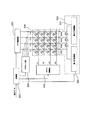
発光素子は、所定電流又は電圧が提供される場合、所定波長を有する光を発する。図1は、従来の発光素子を図示したブロック図である。図1を参照すれば、上記発光素子はパネル100、制御部102、第1スキャン駆動部104、第2スキャン駆動部106、放電部108、プリチャージ部110、及びデータ駆動部112を含む。
The light emitting device emits light having a predetermined wavelength when a predetermined current or voltage is provided. FIG. 1 is a block diagram illustrating a conventional light emitting device. Referring to FIG. 1, the light emitting device includes a
パネル100は、データラインD1〜D4とスキャンラインS1〜S4が交差する発光領域に形成される複数のピクセルE11〜E44を含む。
The
制御部102は、外部装置から表示データを受信し、上記受信された表示データを用いてスキャン駆動部104及び106、放電部108、プリチャージ部110、及びデータ駆動部112の動作を制御する。
The
第1スキャン駆動部104は、スキャンラインS1〜S4中の一部(例えば、スキャンラインS1、S3)に第1スキャン信号を伝送する。第2スキャン駆動部106は、他のスキャンラインS2、S4に第2スキャン信号を伝送する。その結果、スキャンラインS1〜S4が順次に接地に接続される。
The
放電部108は、スイッチSW1〜SW4を介してデータラインD1〜D4に接続される。さらに、放電部108は、放電時スイッチSW1〜SW4をターン−オンし、それで、データラインD1〜D4がツェナーダイオード(ZD)に接続される。その結果、データラインD1〜D4がツェナーダイオードのツェナー電圧まで放電される。
プリチャージ部110は、制御部102の制御の下に上記表示データに対応するプリチャージ電流を上記放電されたデータラインD1〜D4に提供する。
The
データ駆動部112は、制御部102の制御の下に上記表示データに対応するデータ信号、即ち、データ電流を上記プリチャージされたデータラインD1〜D4に提供する。その結果、ピクセルE11〜E44は、発光する。
The
図2a及び図2bは、図1の発光素子を概略的に図示した回路図で、図2c及び図2dは、上記発光素子の駆動過程を図示したタイミングダイヤグラムである。以下、第1スキャンラインS1に対応するカソード電圧VC11〜VC41を説明した後、上記発光素子の駆動過程を詳述する。 2A and 2B are circuit diagrams schematically illustrating the light emitting device of FIG. 1, and FIGS. 2C and 2D are timing diagrams illustrating a driving process of the light emitting device. Hereinafter, after describing the cathode voltages VC11 to VC41 corresponding to the first scan line S1, the driving process of the light emitting device will be described in detail.
図2aに示されるように、第11ピクセルE11と上記接地と間の抵抗は、スキャン抵抗Rsであり、第21ピクセルE21と上記接地と間の抵抗は、Rs+Rpである。また、第31ピクセルE31と上記接地と間の抵抗は、Rs+2Rpであり、第41ピクセルE41と上記接地と間の抵抗は、Rs+3Rpである。 As shown in FIG. 2a, the resistance between the eleventh pixel E11 and the ground is a scan resistance Rs, and the resistance between the twenty-first pixel E21 and the ground is Rs + Rp. The resistance between the 31st pixel E31 and the ground is Rs + 2Rp, and the resistance between the 41st pixel E41 and the ground is Rs + 3Rp.
ここで、ピクセルE11〜E41を同じ輝度で発光させるために、同じ大きさのデータ電流I11〜I41が、データラインD1〜D4に提供されると仮定する。 Here, it is assumed that data currents I11 to I41 having the same magnitude are provided to the data lines D1 to D4 in order to cause the pixels E11 to E41 to emit light with the same luminance.
この場合、データ電流I11〜I41が、該当ピクセルE11〜E41及び第1スキャンラインS1を通った後、接地に流れる。従って、ピクセルE11〜E41のカソード電圧VC11〜VC41は、データ電流I11〜I41の大きさが同一になるので、該当抵抗、即ち、ピクセルE11〜E41と上記接地と間の抵抗に比例する大きさを有する。従って、第41カソード電圧VC41、第31カソード電圧VC31、第21カソード電圧VC21、及び第11カソード電圧VC11の順にその大きさが大きくなる。 In this case, the data currents I11 to I41 flow to the ground after passing through the corresponding pixels E11 to E41 and the first scan line S1. Accordingly, the cathode voltages VC11 to VC41 of the pixels E11 to E41 have the same magnitudes of the data currents I11 to I41, and therefore have a resistance proportional to the resistance between the pixels E11 to E41 and the ground. Have. Accordingly, the 41st cathode voltage VC41, the 31st cathode voltage VC31, the 21st cathode voltage VC21, and the 11th cathode voltage VC11 increase in order.
図2bを参照すれば、第12ピクセルE12と上記接地と間の抵抗は、Rs+3Rpであり、第11ピクセルE11と上記接地と間の抵抗より大きい。ここで、第1スキャンラインS1が接地に接続される時に第1データラインD1に流れるデータ電流と、第2スキャンラインS2とが接地に接続される時に第1データラインD1に流れるデータ電流の大きさが同一と仮定する。この場合、ピクセルE11及びE12のカソード電圧VC11及びVC12が該当抵抗に比例する大きさを有するので、第12カソード電圧VC12が第11カソード電圧VC11より大きい。 Referring to FIG. 2b, the resistance between the twelfth pixel E12 and the ground is Rs + 3Rp, which is larger than the resistance between the eleventh pixel E11 and the ground. Here, the magnitude of the data current flowing through the first data line D1 when the first scan line S1 is connected to the ground and the data current flowing through the first data line D1 when the second scan line S2 is connected to the ground. Are assumed to be the same. In this case, since the cathode voltages VC11 and VC12 of the pixels E11 and E12 have a magnitude proportional to the corresponding resistance, the twelfth cathode voltage VC12 is larger than the eleventh cathode voltage VC11.
以下、上記発光素子を駆動する過程を詳述する。
スイッチSW1〜SW6がターン−オンされ、スキャンラインS1〜S4が上記発光素子の駆動電圧、例えば、データ電流の最大輝度に対応する電圧と同じ大きさの電圧V2を有する非発光源に接続される。従って、ピクセルE11〜E44は発光せず、データラインD1〜D4は、第1放電時間dcha1の間、ツェナーダイオードのツェナー電圧まで同一に放電される。
Hereinafter, a process of driving the light emitting device will be described in detail.
The switches SW1 to SW6 are turned on, and the scan lines S1 to S4 are connected to a non-light emitting source having a driving voltage of the light emitting element, for example, a voltage V2 having the same magnitude as the voltage corresponding to the maximum luminance of the data current. . Accordingly, the pixels E11 to E44 do not emit light, and the data lines D1 to D4 are discharged to the same Zener diode voltage during the first discharge time dcha1.
次いで、スイッチSW1〜SW4がターン−オフされた後、第1表示データに対応するプリチャージ電流が、図2c及び図2dに示されるように、第1プリチャージ時間pcha1の間、データラインD1〜D4に提供される。 Next, after the switches SW1 to SW4 are turned off, the precharge current corresponding to the first display data is applied to the data lines D1 to D1 during the first precharge time pcha1, as shown in FIGS. 2c and 2d. Provided to D4.
続いて、第1スキャンラインS1が、図2aに示されるように、接地に接続され、他のスキャンラインS2〜S4は、上記非発光源に接続される。 Subsequently, the first scan line S1 is connected to ground as shown in FIG. 2a, and the other scan lines S2 to S4 are connected to the non-light emitting source.
次いで、第1表示データに対応するデータ電流I11、I21、I31、I41が、データラインD1〜D4に提供される。その結果、ピクセルE11〜E41が第1発光時間t1の間発光する。 Next, data currents I11, I21, I31, and I41 corresponding to the first display data are provided to the data lines D1 to D4. As a result, the pixels E11 to E41 emit light during the first light emission time t1.
以下、第41ピクセルE41と第11ピクセルE11とが同じ輝度で発光するように既設定されたと仮定する。即ち、第1データラインD1と第4データラインD4に同じ大きさのデータ電流I11、I41が、第1発光時間t1の間提供される。 Hereinafter, it is assumed that the 41st pixel E41 and the 11th pixel E11 are already set to emit light with the same luminance. That is, the same data currents I11 and I41 are provided to the first data line D1 and the fourth data line D4 during the first light emission time t1.
まず、放電時に、データラインD1、D4が、図2dに示されるように、第1放電時間dcha1の間、同じ大きさの放電電圧まで放電され、それで、データラインD1、D4が、第1プリチャージ時間pcha1の間同じレベル、即ち、所定プリチャージ電圧までプリチャージされる。 First, at the time of discharging, as shown in FIG. 2d, the data lines D1 and D4 are discharged to the same discharge voltage during the first discharge time dcha1, so that the data lines D1 and D4 are It is precharged to the same level during the charge time pcha1, that is, to a predetermined precharge voltage.
次いで、同じ大きさのデータ電流I11及びI41が、第1データラインD1と第4データラインD4にそれぞれ提供される。この場合、ピクセルE11〜E41が同じ輝度で発光するように既設定されたので、ピクセルE11及びE41のアノード電圧VA11、VA41は、上記プリチャージ電圧から該当カソード電圧VC11、VC41より所定レベルの差を有する電圧まで上昇された後、安定化される。なぜならば、ピクセルがそのアノード電圧とそのカソード電圧との差に対応する輝度で発光するからである。例えば、ピクセルE11のカソード電圧VC11が1Vであり、ピクセルE41のカソード電圧VC41が2Vであるならば、ピクセルE11のアノード電圧VA11が6Vで安定化される時、ピクセルE41のアノード電圧VA41は、7Vで安定化される。 Next, data currents I11 and I41 having the same magnitude are provided to the first data line D1 and the fourth data line D4, respectively. In this case, since the pixels E11 to E41 are set to emit light with the same luminance, the anode voltages VA11 and VA41 of the pixels E11 and E41 have a predetermined level difference from the corresponding cathode voltages VC11 and VC41 from the precharge voltage. After being raised to the voltage it has, it is stabilized. This is because the pixel emits light with a luminance corresponding to the difference between its anode voltage and its cathode voltage. For example, if the cathode voltage VC11 of the pixel E11 is 1V and the cathode voltage VC41 of the pixel E41 is 2V, the anode voltage VA41 of the pixel E41 is 7V when the anode voltage VA11 of the pixel E11 is stabilized at 6V. It is stabilized with.
この場合、データラインD1、D4が同じレベル、例えば、3Vでプリチャージされたので、ピクセルE11のアノード電圧VA11は、3Vから6Vまで上昇した後、安定化されるが、ピクセルE41のアノード電圧VA41は、3Vから7Vまで上昇した後、安定化される。 In this case, since the data lines D1 and D4 are precharged at the same level, for example, 3V, the anode voltage VA11 of the pixel E11 rises from 3V to 6V and then stabilizes, but the anode voltage VA41 of the pixel E41. Is stabilized after rising from 3V to 7V.
従って、ピクセルE41のアノード電圧VA41が安定化されるまで消耗される電荷量は、図2dに示されるように、ピクセルE11のアノード電圧VA11が安定化されるまで消耗される電荷量より大きくなる。従って、ピクセルE11及びE41が同じ輝度で発光するように既設定されたにもかかわらず、ピクセルE41がピクセルE11より暗く発光する。 Accordingly, the amount of charge consumed until the anode voltage VA41 of the pixel E41 is stabilized is larger than the amount of charge consumed until the anode voltage VA11 of the pixel E11 is stabilized, as shown in FIG. 2d. Therefore, although the pixels E11 and E41 are already set to emit light with the same luminance, the pixel E41 emits light darker than the pixel E11.
以下、上記発光素子駆動過程を詳述する。
スキャンラインS1〜S4が上記非発光源に接続され、スイッチSW1〜SW4がターン−オンされる。その結果、データラインD1〜D4が、図2cに示されるように、第2放電時間dcha2の間、所定放電電圧まで放電される。
Hereinafter, the light emitting element driving process will be described in detail.
The scan lines S1 to S4 are connected to the non-light emitting source, and the switches SW1 to SW4 are turned on. As a result, the data lines D1 to D4 are discharged to a predetermined discharge voltage during the second discharge time dcha2, as shown in FIG. 2c.
次いで、スイッチSW1〜SW4がターン−オフなった後第2表示データに対応するプリチャージ電流がデータラインD1〜D4に提供される。ここで、上記第2表示データは、上記第1表示データが制御部102に入力された後、入力されるデータである。
Next, after the switches SW1 to SW4 are turned off, a precharge current corresponding to the second display data is provided to the data lines D1 to D4. Here, the second display data is data input after the first display data is input to the
続いて、第2スキャンラインS2が、図2bに示されるように、上記接地に接続され、他のスキャンラインS1、S3及びS4が上記非発光源に接続される。次いで、上記第2表示データに対応するデータ電流I12、I22、I32及びI42がデータラインD1〜D4に提供され、それで、ピクセルE12〜E42が第2発光時間t2の間発光する。 Subsequently, as shown in FIG. 2b, the second scan line S2 is connected to the ground, and the other scan lines S1, S3, and S4 are connected to the non-light emitting source. Next, data currents I12, I22, I32 and I42 corresponding to the second display data are provided to the data lines D1 to D4, so that the pixels E12 to E42 emit light during the second light emission time t2.
以下、第11ピクセルE11と第12ピクセルE12とが同じ輝度で発光するように設計されたと仮定する。即ち、第11ピクセルE11と第12ピクセルE12に同じ大きさのデータ電流I11及びI12が提供される。 Hereinafter, it is assumed that the eleventh pixel E11 and the twelfth pixel E12 are designed to emit light with the same luminance. That is, the same data currents I11 and I12 are provided to the eleventh pixel E11 and the twelfth pixel E12.
この場合、ピクセルE12と接地と間の抵抗がピクセルE11と接地と間の抵抗より大きいため、ピクセルE12のカソード電圧VC12がピクセルE11のカソード電圧VC11より大きく、それで、ピクセルE12のアノード電圧VA12が安定化されるまで消耗される電荷量は、ピクセルE11のアノード電圧VA11が安定化されるまで消耗される電荷量より大きい。従って、ピクセルE12がピクセルE11より暗く発光する。このように、同じ輝度で発光するように設定されたピクセルが互いに異なる輝度で発光する現状をクロストーク現像(Cross-talk Phenomenon)という。 In this case, since the resistance between the pixel E12 and the ground is larger than the resistance between the pixel E11 and the ground, the cathode voltage VC12 of the pixel E12 is larger than the cathode voltage VC11 of the pixel E11, so that the anode voltage VA12 of the pixel E12 is stable. The amount of charge consumed until the anode voltage VA11 is consumed is larger than the amount of charge consumed until the anode voltage VA11 of the pixel E11 is stabilized. Accordingly, the pixel E12 emits light darker than the pixel E11. The current situation in which pixels set to emit light with the same brightness emit light with different brightness is called cross-talk development (Cross-talk Phenomenon).
本発明の目的は、クロストーク現像が生じない発光素子及びその駆動方法を提供するものである。 An object of the present invention is to provide a light emitting element that does not cause crosstalk development and a driving method thereof.
上記目的を達成するために、本発明の好ましい第1の実施形態に係る発光素子は、データライン、スキャンライン、ピクセル、及び放電部を含む。上記データラインは、第1方向に配列され、上記スキャンラインは、上記第1方向と異なる方向の第2方向に配列される。上記ピクセルは、上記データラインと上記スキャンラインとが交差する発光領域に形成される。上記放電部は、上記ピクセル中の第1ピクセルを、第1放電時間の間第1放電電圧まで放電させて、上記ピクセル中の第2ピクセルを、第2放電時間の間第2放電電圧まで放電する。ここで、上記第2放電電圧は、上記第1放電電圧と異なる大きさを有する。 In order to achieve the above object, a light emitting device according to a first embodiment of the present invention includes a data line, a scan line, a pixel, and a discharge unit. The data lines are arranged in a first direction, and the scan lines are arranged in a second direction different from the first direction. The pixel is formed in a light emitting region where the data line and the scan line intersect. The discharge unit discharges a first pixel in the pixel to a first discharge voltage during a first discharge time, and discharges a second pixel in the pixel to a second discharge voltage during a second discharge time. To do. Here, the second discharge voltage has a magnitude different from that of the first discharge voltage.
本発明の好ましい第2の実施形態に係る発光素子は、データライン、スキャンライン、ピクセル、及び放電部を含む。上記データラインは、第1方向に配列され、上記スキャンラインは、上記第1方向と異なる方向の第2方向に配列される。上記ピクセルは、上記データラインと上記スキャンラインとが交差する領域に形成される。上記放電部は、少なくとも一つの放電補助素子を有し、少なくとも一つのデータラインを該当ピクセルのカソード電圧に対応する放電電圧まで放電する。ここで、上記放電補助素子は、上記放電を促進する。 The light emitting device according to the second embodiment of the present invention includes a data line, a scan line, a pixel, and a discharge unit. The data lines are arranged in a first direction, and the scan lines are arranged in a second direction different from the first direction. The pixel is formed in a region where the data line and the scan line intersect. The discharge unit includes at least one discharge assisting element, and discharges at least one data line to a discharge voltage corresponding to the cathode voltage of the corresponding pixel. Here, the discharge assisting element promotes the discharge.
本発明の好ましい第3の実施形態に係る放電素子は、データライン、スキャンライン、ピクセル、及び放電部を含む。上記データラインは、第1方向に配列され、上記スキャンラインは、上記第1方向と異なる第2方向に配列される。上記ピクセルは、上記データラインと上記スキャンラインとが交差する領域に形成される。上記放電部は、少なくとも一つのデータラインを、放電時間中の第1サブ放電時間の間、第1放電電圧まで放電し、上記放電時間中の第2サブ放電時間の間、上記放電されたデータラインを該当ピクセルのカソード電圧に対応する第2放電電圧まで放電する。ここで、上記第2サブ放電時間は、上記第2放電電圧の大きさに対応して変わる。 The discharge element according to the third exemplary embodiment of the present invention includes a data line, a scan line, a pixel, and a discharge unit. The data lines are arranged in a first direction, and the scan lines are arranged in a second direction different from the first direction. The pixel is formed in a region where the data line and the scan line intersect. The discharge unit discharges at least one data line to a first discharge voltage during a first sub-discharge time during a discharge time, and discharges the data during a second sub-discharge time during the discharge time. The line is discharged to a second discharge voltage corresponding to the cathode voltage of the corresponding pixel. Here, the second sub-discharge time varies according to the magnitude of the second discharge voltage.
本発明の好ましい第1の実施形態に係るデータラインとスキャンラインとが交差する発光領域に形成される複数のピクセルを含む発光素子を駆動する方法は、上記データラインの最外郭データライン中の第1最外郭データラインに第1電圧を提供する段階と、上記最外郭データライン中の第2最外郭データラインに第2電圧を提供する段階とを含む。ここで、少なくとも一つのデータラインは、上記提供された電圧によって、該当ピクセルのカソード電圧及び上記ピクセルに寄生するキャパシタのキャパシタンスに対応する放電電圧まで放電される。上記発光素子駆動方法は、上記データラインを所定放電電圧まで放電する段階をさらに含む。上記第1電圧を提供する段階は、外部から入力された第1外部電圧によって第1レベル電圧を出力する段階と、上記第1最外郭データラインが上記第1電圧を有するように上記出力された第1レベル電圧によって、上記第1最外郭データラインに所定電圧を提供する段階とを含む。上記第2電圧を提供する段階は、外部から入力された第2外部電圧によって第2レベル電圧を出力する段階と、上記第2最外郭データラインが上記第2電圧を有するように上記出力された第2レベル電圧によって、上記第2最外郭データラインに所定電圧を提供する段階とを含む。上記第2電圧は、上記第1電圧と異なる大きさを有することができる。 A method of driving a light emitting device including a plurality of pixels formed in a light emitting region where a data line and a scan line intersect according to a first preferred embodiment of the present invention includes a method for driving a light emitting element in an outermost data line of the data line. Providing a first voltage to one outermost data line; and providing a second voltage to a second outermost data line in the outermost data line. Here, at least one data line is discharged to the discharge voltage corresponding to the cathode voltage of the pixel and the capacitance of the capacitor parasitic to the pixel by the provided voltage. The light emitting device driving method further includes a step of discharging the data line to a predetermined discharge voltage. The providing of the first voltage includes outputting a first level voltage according to a first external voltage input from the outside, and outputting the first outermost data line to have the first voltage. Providing a predetermined voltage to the first outermost data line according to a first level voltage. The providing of the second voltage includes outputting a second level voltage according to a second external voltage input from the outside, and outputting the second outermost data line to have the second voltage. Providing a predetermined voltage to the second outermost data line according to a second level voltage. The second voltage may have a magnitude different from the first voltage.
本発明の好ましい第2の実施形態に係るデータラインとスキャンラインが交差する発光領域に形成される複数のピクセルを含む発光素子を駆動する方法は、第1ピクセルに対応する第1データラインを、第1放電時間の間放電する段階と、第2ピクセルに対応する第2データラインを、第2放電時間の間放電する段階と、上記放電された第1データラインに第1データ電流を提供する段階と、及び上記放電された第2データラインに第2データ電流を提供する段階とを含む。ここで、上記第1データラインが有する電圧の信号波形における上記第1放電時間の終端点での電圧と、上記第2データラインが有する電圧の信号波形における上記第2放電時間の終端点での電圧との間の大きさの差は、上記ピクセルのカソード電圧の大きさの差及び上記ピクセルに寄生するキャパシタ等のキャパシタンス差に対応する。 A method of driving a light emitting device including a plurality of pixels formed in a light emitting region where a data line and a scan line intersect according to a second preferred embodiment of the present invention includes: a first data line corresponding to a first pixel; Discharging for a first discharge time; discharging a second data line corresponding to the second pixel for a second discharge time; and providing a first data current to the discharged first data line. And providing a second data current to the discharged second data line. Here, the voltage at the end point of the first discharge time in the signal waveform of the voltage included in the first data line and the end point of the second discharge time in the signal waveform of the voltage included in the second data line. The difference in magnitude with respect to the voltage corresponds to the difference in magnitude of the cathode voltage of the pixel and the capacitance difference such as a capacitor parasitic to the pixel.
本発明の好ましい第3の実施形態に係るデータラインとスキャンラインとが交差する発光領域に形成される複数のピクセルを含む発光素子を駆動する方法は、上記データラインの最外郭データライン中の第1最外郭データラインに第1電圧を提供する段階と、上記最外郭データライン中の第2最外郭データラインに第2電圧を提供すると段階を含む。ここで、少なくとも一つのデータラインは、上記提供された電圧によって該当ピクセルのカソード電圧に対応する放電電圧まで放電され、上記放電は、上記データラインに接続された放電補助素子により促進される。上記放電補助素子は、OPアンプであってもよい。 According to a third exemplary embodiment of the present invention, a method for driving a light emitting device including a plurality of pixels formed in a light emitting region where a data line and a scan line intersect with each other is the Providing a first voltage to one outermost data line; and providing a second voltage to a second outermost data line in the outermost data line. Here, at least one data line is discharged to a discharge voltage corresponding to the cathode voltage of the corresponding pixel by the provided voltage, and the discharge is promoted by a discharge assisting element connected to the data line. The discharge assist element may be an OP amplifier.
本発明の好ましい第4の実施形態に係るデータラインとスキャンラインとが交差する発光領域に形成される複数のピクセルを含む発光素子を駆動する方法は、第1ピクセルに対応する第1データラインを、第1放電時間の間放電する段階と、第2ピクセルに対応する第2データラインを、第2放電時間の間放電する段階と、第1データ電流を上記放電された第1データラインに提供する段階と、第2データ電流を上記放電された第2データラインに提供すると段階を含む。ここで、上記第1データラインが有する電圧の変化波形における上記第1放電時間の終端点での電圧と、上記第2データラインが有する電圧の変化波形における上記第2放電時間の終端点での電圧との間の大きさの差は、上記ピクセルのカソード電圧の大きさの差に対応し、上記放電は、放電補助素子により促進される。 According to a fourth exemplary embodiment of the present invention, a method of driving a light emitting device including a plurality of pixels formed in a light emitting region where a data line and a scan line intersect each other includes: Discharging for a first discharge time; discharging a second data line corresponding to the second pixel for a second discharge time; and providing a first data current to the discharged first data line. And providing a second data current to the discharged second data line. Here, the voltage at the end point of the first discharge time in the voltage change waveform of the first data line and the end point of the second discharge time in the voltage change waveform of the second data line. The magnitude difference between the voltages corresponds to the magnitude difference in the cathode voltage of the pixel, and the discharge is promoted by a discharge assisting element.
本発明の好ましい第5の実施形態に係るデータラインとスキャンラインとが交差する発光領域に形成される複数のピクセルを含む発光素子を駆動する方法は、少なくとも一つのデータラインを、放電時間中の第1サブ放電時間の間第1放電電圧まで放電する段階と、上記放電時間中の第2サブ放電時間の間、上記放電されたデータラインを該当ピクセルのカソード電圧に対応する第2放電電圧まで放電する段階とを含む。ここで、上記第2サブ放電時間は、上記第2放電電圧の大きさに対応して変わる。上記第2放電電圧まで放電する段階は、上記データラインの最外郭データライン中の第1最外郭データラインに第1電圧を提供する段階と、上記最外郭データライン中の第2最外郭データラインに第2電圧を提供する段階とを含む。上記第2電圧は、上記第1電圧と異なる大きさを有していてもよい。 According to a fifth exemplary embodiment of the present invention, there is provided a method for driving a light emitting device including a plurality of pixels formed in a light emitting region where a data line and a scan line intersect with each other. Discharging to a first discharge voltage during a first sub-discharge time, and during a second sub-discharge time during the discharge time, discharging the discharged data line to a second discharge voltage corresponding to the cathode voltage of the corresponding pixel. Discharging. Here, the second sub-discharge time varies according to the magnitude of the second discharge voltage. The discharging to the second discharge voltage includes providing a first voltage to a first outermost data line in the outermost data line of the data line, and a second outermost data line in the outermost data line. Providing a second voltage. The second voltage may have a magnitude different from the first voltage.
本発明の好ましい第6の実施形態に係るデータラインとスキャンラインとが交差する発光領域に形成される複数のピクセルを含む発光素子を駆動する方法は、第1ピクセルに対応する第1データラインと第2ピクセルに対応する第2データラインを、第1サブ放電時間の間第1放電電圧まで放電する段階と、上記放電された第1データラインを、第2サブ放電時間の間第2放電電圧まで放電する段階と、上記放電された第2データラインを、第3サブ放電時間の間第3放電電圧まで放電する段階とを含む。ここで、上記第1データラインが有する電圧の変化波形における上記第2サブ放電時間の終端点での電圧と、上記第2データラインが有する電圧の変化波形における上記第3サブ放電時間の終端点での電圧との間の大きさの差は、上記ピクセルのカソード電圧の大きさの差に対応し、上記第2サブ放電時間は、上記第2放電電圧の大きさに対応して変わる。 A method of driving a light emitting device including a plurality of pixels formed in a light emitting region where a data line and a scan line intersect according to a sixth preferred embodiment of the present invention includes: a first data line corresponding to the first pixel; Discharging a second data line corresponding to the second pixel to a first discharge voltage during a first sub-discharge time; and discharging the discharged first data line during a second sub-discharge time. And discharging the discharged second data line to a third discharge voltage for a third sub-discharge time. Here, the voltage at the end point of the second sub-discharge time in the voltage change waveform of the first data line, and the end point of the third sub-discharge time in the voltage change waveform of the second data line. The magnitude difference between the first and second voltages corresponds to the magnitude of the cathode voltage of the pixel, and the second sub-discharge time varies according to the magnitude of the second discharge voltage.
本発明に係る発光素子及びその駆動方法によれば、放電電圧が該当スキャンライン抵抗及び該当ピクセルに寄生するキャパシタのキャパシタンスに対応して変わるので、上記発光素子にクロストーク現像が生じない。
また、本発明に係る発光素子及びその駆動方法によれば、放電電圧がカソード電圧によって変わるので、クロストーク現像が生じない。
さらに、本発明に係る発光素子及びその駆動方法によれば、データライン間の抵抗Rdが増加されるので、消費電力が低減する。
さらに、本発明に係る発光素子及びその駆動方法によれば、第2サブ放電時間の間OPアンプに抵抗値が異なる抵抗が選択的に接続されるので、上記第2放電時間が最適に形成されうる。
According to the light emitting device and the driving method thereof according to the present invention, since the discharge voltage changes corresponding to the corresponding scan line resistance and the capacitance of the capacitor parasitic to the corresponding pixel, no crosstalk development occurs in the light emitting device.
Further, according to the light emitting device and the driving method thereof according to the present invention, since the discharge voltage varies depending on the cathode voltage, crosstalk development does not occur.
Furthermore, according to the light emitting device and the driving method thereof according to the present invention, the resistance Rd between the data lines is increased, so that the power consumption is reduced.
Furthermore, according to the light emitting device and the driving method thereof according to the present invention, since the resistors having different resistance values are selectively connected to the OP amplifier during the second sub-discharge time, the second discharge time is optimally formed. sell.
以下では、添付図面を参照して、本発明に係る発光素子及びその駆動方法の好ましい実施形態を詳細に説明する。 Hereinafter, preferred embodiments of a light emitting device and a driving method thereof according to the present invention will be described in detail with reference to the accompanying drawings.
図3は、本発明の好ましい第1の実施形態に係る発光素子を図示したブロック図である。
図3を参照すれば、本実施形態の発光素子は、パネル300、制御部302、第1スキャン駆動部304、第2スキャン駆動部306、放電部308、プリチャージ部310、及びデータ駆動部312を含む。
FIG. 3 is a block diagram illustrating a light emitting device according to the first embodiment of the present invention.
Referring to FIG. 3, the light emitting device of the present embodiment includes a
本発明の好ましい一実施形態に係る発光素子は、有機電界発光素子(Organic Electroluminescent Device)、PDP(Plasma Display Panel)、LCD(Liquid Crystal Display)などを含む。但し、以下では、説明の便宜のために、上記有機電界発光素子を例として説明する。 A light emitting device according to a preferred embodiment of the present invention includes an organic electroluminescent device, a PDP (Plasma Display Panel), an LCD (Liquid Crystal Display) and the like. However, in the following, for the convenience of explanation, the organic electroluminescent element will be described as an example.
パネル300は、データラインD1〜D4とスキャンラインS1〜Sと4が交差する発光領域に形成される複数のピクセルE11〜E44を含む。
The
上記発光素子が有機電界発光素子の場合、各ピクセルE11〜E44は、基板上に順次に形成されるアノード電極層、有機物層、及びカソード電極層を含む。 When the light emitting device is an organic electroluminescent device, each of the pixels E11 to E44 includes an anode electrode layer, an organic material layer, and a cathode electrode layer that are sequentially formed on the substrate.
制御部302は、外部から表示データ、例えば、RGBデータを受信し、上記受信された表示データを用いてスキャン駆動部304及び306、放電部308、プリチャージ部310、及びデータ駆動部312の動作を制御する。また、制御部302は、上記受信された表示データを外部またはその内部に貯蔵することができる。
The
第1スキャン駆動部304は、スキャンラインS1〜S4中の一部(例えば、S1、S3)に第1スキャン信号を伝送する。第2スキャン駆動部306は、他のスキャンラインS2及びS4に第2スキャン信号を伝送する。その結果、スキャンラインS1〜S4が順次に低位スキャン電圧を有する発光源、好ましくは接地に接続される。以下、上記発光源を接地として仮定する。
The
放電部308は、少なくとも一つのデータラインを該当ピクセルのカソード電圧に対応する放電電圧まで放電する素子であり、第1サブ放電部320及び第2サブ放電部322を含む。ここで、上記カソード電圧は、該当スキャンラインの抵抗値(以下、“スキャンライン抵抗”という)及び上記スキャンラインを介して流れるデータ電流に対応する値を有する。
The
本発明の一実施形態に係る発光素子において、放電部308は、上記データラインを上記カソード電圧に対応する上記放電電圧まで放電するが、この場合、上記データラインに対応するピクセルに寄生するキャパシタのキャパシタンス値を考慮する。
In the light emitting device according to an embodiment of the present invention, the
本発明の他の実施形態に係る発光素子では、放電部308は、データラインD1〜D4をピクセルE11〜E44のカソード電圧に対応する放電電圧まで放電する。
In the light emitting device according to another embodiment of the present invention, the
第1サブ放電部320は、図3に示されるように、スイッチSW1を介してデータラインD1及びD4中の第1最外郭データラインD1に接続され、そして、放電時、第1最外郭データラインD1に第1電圧を提供する。
As shown in FIG. 3, the first
第2サブ放電部322は、スイッチSW4を介して、データラインD1及びD4中の第2最外郭データラインD4に接続され、そして、第2最外郭データラインD4に第2電圧を提供する。
The second
本発明の一実施形態に係る発光素子では、上記第2電圧は、上記第1電圧と異なる大きさを有する。サブ放電部320、322に対する詳細な説明は、以下添付図面を参照して詳述する。
In the light emitting device according to the embodiment of the present invention, the second voltage has a magnitude different from that of the first voltage. A detailed description of the
プリチャージ部310は、制御部302の制御の下に上記表示データに対応するプリチャージ電流を、上記放電されたデータラインD1〜D4に提供する。
The
データ駆動部312は、制御部302の制御の下に上記表示データに対応するデータ信号、即ち、データ電流を、上記プリチャージされたデータラインD1〜D4に提供する。その結果、ピクセルE11〜E44が発光する。
The
以下、本発明の発光素子駆動過程を詳述する。但し、複数の表示データが順次に制御部302に入力されると仮定する。
Hereinafter, the light emitting device driving process of the present invention will be described in detail. However, it is assumed that a plurality of display data are sequentially input to the
第1スキャンラインS1が発光源、好ましくは接地に接続され、他のスキャンラインS2〜S4は上記発光素子の駆動電圧、例えば、データ電流の最大輝度に対応する電圧と同じ大きさの電圧を有する非発光源に接続される。 The first scan line S1 is connected to a light emitting source, preferably ground, and the other scan lines S2 to S4 have a driving voltage of the light emitting element, for example, a voltage having the same magnitude as the voltage corresponding to the maximum brightness of the data current. Connected to a non-luminescent source.
その後、第1表示データに対応する第1データ電流がデータラインD1〜D4に提供される。この場合、上記第1データ電流は、データラインD1〜D4及びこれに対応するピクセルE11〜E41を通った後、第1スキャンラインS1を介して上記接地に流れる。その結果、第1スキャンラインS1に対応するピクセルE11〜E41が発光する。 Thereafter, a first data current corresponding to the first display data is provided to the data lines D1 to D4. In this case, the first data current flows through the data lines D1 to D4 and the corresponding pixels E11 to E41, and then flows to the ground via the first scan line S1. As a result, the pixels E11 to E41 corresponding to the first scan line S1 emit light.
次いで、データラインD1〜D4は、放電時間の間、ピクセルE12〜E42のカソード電圧に対応する放電電圧まで放電される。 The data lines D1-D4 are then discharged to a discharge voltage corresponding to the cathode voltages of the pixels E12-E42 during the discharge time.
続いて、データラインD1〜D4が、上記第1表示データ入力後に制御部302に入力される第2表示データに対応するプリチャージ電圧までプリチャージされる。
Subsequently, the data lines D1 to D4 are precharged up to a precharge voltage corresponding to the second display data input to the
その後、第2スキャンラインS2が接地に接続され、他のスキャンラインS1、S3、S4は上記非発光源に接続される。 Thereafter, the second scan line S2 is connected to the ground, and the other scan lines S1, S3, S4 are connected to the non-light emitting source.
次いで、上記第2表示データに対応する第2データ電流が、データラインD1〜D4に提供される。その結果、第2スキャンラインS2に対応するピクセルE12〜E42が発光する。続いて、データラインD1〜D4が、放電時間の間放電される。 Next, a second data current corresponding to the second display data is provided to the data lines D1 to D4. As a result, the pixels E12 to E42 corresponding to the second scan line S2 emit light. Subsequently, the data lines D1 to D4 are discharged during the discharge time.
上記のような発光過程を第4スキャンラインS4まで繰り返し、その後、第1スキャンラインS1から第4スキャンラインS4単位で、即ち、フレーム単位で上記発光過程を繰り返す。 The light emission process as described above is repeated up to the fourth scan line S4, and then the light emission process is repeated from the first scan line S1 to the fourth scan line S4, that is, in units of frames.
図4a及び図4bは、図3の発光素子を概略的に図示した回路図で、図4c及び図4dは、上記発光素子の駆動過程を図示したタイミングダイヤグラムである。
図4aを参照すれば、第1サブ放電部320は、第1スイッチSW5(400)、第1デジタル−アナログ変換器402(第1DAC)、及び第1OPアンプ404を含む。
4A and 4B are circuit diagrams schematically illustrating the light emitting device of FIG. 3, and FIGS. 4C and 4D are timing diagrams illustrating a driving process of the light emitting device.
Referring to FIG. 4A, the first
第2サブ放電部322は、第2スイッチSW6(406)、第2DAC408、及び第2OPアンプ410を含む。
The second
以下、カソード電圧VC11〜VC44を説明した後、上記発光素子の駆動過程を詳述する。 Hereinafter, after describing the cathode voltages VC11 to VC44, the driving process of the light emitting element will be described in detail.
第1スキャンラインS1に対応するピクセルE11〜E44のカソード電圧VC11〜VC41の大きさを比較する。 The magnitudes of the cathode voltages VC11 to VC41 of the pixels E11 to E44 corresponding to the first scan line S1 are compared.
図4aに示されるように、第11ピクセルE11と上記接地と間の抵抗、即ち、スキャンライン抵抗は、スキャン抵抗Rsであり、第21ピクセルE21と上記接地と間のスキャンライン抵抗は、Rs+Rpである。また、第31ピクセルE31と上記接地と間のスキャンライン抵抗は、Rs+2Rpであり、第41ピクセルE41と上記接地と間のスキャンライン抵抗は、Rs+3Rpである。 As shown in FIG. 4a, the resistance between the eleventh pixel E11 and the ground, that is, the scan line resistance is a scan resistance Rs, and the scan line resistance between the twenty-first pixel E21 and the ground is Rs + Rp. is there. The scan line resistance between the 31st pixel E31 and the ground is Rs + 2Rp, and the scan line resistance between the 41st pixel E41 and the ground is Rs + 3Rp.
ここで、ピクセルE11〜E41を同じ輝度で発光させるために、同じ大きさのデータ電流I11〜I41が、データラインD1〜D4に提供されると仮定する。この場合、データ電流I11〜I41が、該当ピクセルE11〜E41及び第1スキャンラインS1を通った後、接地に流れる。従って、ピクセルE11〜E41のカソード電圧VC11〜VC41は、データ電流I11〜I41の大きさが同一なので、該当抵抗、即ち、ピクセルE11〜E41と上記接地と間の抵抗に比例する大きさを有する。従って、第41カソード電圧VC41、第31カソード電圧VC31、第21カソード電圧VC21、及び第11カソード電圧VC11の順でその大きさが大きくなる。 Here, it is assumed that data currents I11 to I41 having the same magnitude are provided to the data lines D1 to D4 in order to cause the pixels E11 to E41 to emit light with the same luminance. In this case, the data currents I11 to I41 flow to the ground after passing through the corresponding pixels E11 to E41 and the first scan line S1. Accordingly, the cathode voltages VC11 to VC41 of the pixels E11 to E41 have a magnitude proportional to the corresponding resistance, that is, the resistance between the pixels E11 to E41 and the ground, since the magnitudes of the data currents I11 to I41 are the same. Therefore, the 41st cathode voltage VC41, the 31st cathode voltage VC31, the 21st cathode voltage VC21, and the 11th cathode voltage VC11 increase in this order.
図4bを参照すれば、第12ピクセルE12と上記接地と間の抵抗はRs+3Rpであり、第11ピクセルE11と上記接地と間の抵抗より大きい。ここで、第1スキャンラインS1が接地に接続される時に第1データラインD1に流れるデータ電流と、第2スキャンラインS2が接地に接続される時に第1データラインD1に流れるデータ電流の大きさが同じであると仮定する。この場合、ピクセルE11、E12のカソード電圧VC11、VC12が該当抵抗に比例する大きさを有するので、第12カソード電圧VC12の方が第11カソード電圧VC11より大きい。 Referring to FIG. 4b, the resistance between the twelfth pixel E12 and the ground is Rs + 3Rp, which is larger than the resistance between the eleventh pixel E11 and the ground. Here, the magnitude of the data current flowing through the first data line D1 when the first scan line S1 is connected to the ground, and the magnitude of the data current flowing through the first data line D1 when the second scan line S2 is connected to the ground. Are the same. In this case, since the cathode voltages VC11 and VC12 of the pixels E11 and E12 have a magnitude proportional to the corresponding resistance, the twelfth cathode voltage VC12 is larger than the eleventh cathode voltage VC11.
以下、上記発光素子駆動過程を、図4a〜図4dを参照して詳述する。 Hereinafter, the light emitting element driving process will be described in detail with reference to FIGS. 4A to 4D.
放電部308は、データラインD1〜D4を放電する。以下、データラインD1〜D4を放電する過程を詳細に説明する。
The
第1スイッチSW5及び第2スイッチSW6がターン−オンされ、スキャンラインS1〜S4が上記非発光源に接続される。従って、ピクセルE11〜E44は発光しない。 The first switch SW5 and the second switch SW6 are turned on, and the scan lines S1 to S4 are connected to the non-light emitting source. Accordingly, the pixels E11 to E44 do not emit light.
次いで、第1DAC402は、外部から入力される第1外部電圧V3によって第1レベル電圧を出力し、上記出力された第1レベル電圧は、第1OPアンプ404に入力される。また、第2DAC408は、外部から入力される第2外部電圧V4によって第2レベル電圧を出力し、上記出力された第2レベル電圧は、第2OPアンプ410に入力される。
Next, the
続いて、第1OPアンプ404は、上記入力された第1レベル電圧によって第1最外郭データラインD1に第1OPアンプ出力電圧を提供し、それで、第1最外郭データラインD1は、第1電圧を有する。また、第2OPアンプ410は、上記入力された第2レベル電圧によって第2最外郭データラインD4に第2OPアンプ出力電圧を提供し、それで、第2最外郭データラインD4は、第2電圧を有する。ここで、本発明の一実施形態によれば、上記第2電圧は、上記第1電圧と異なる大きさを有する。また、上の場合には第41カソード電圧VC41が第11カソード電圧VC11より大きいので、上記第2電圧の方が上記第1電圧より大きい。
Subsequently, the
このように、第1最外郭データラインD1が上記第1電圧を有して、第2最外郭データラインD4が上記第2電圧を有すれば、データラインD1〜D4は、抵抗Rdによる電圧分配によって順次的な大きさの電圧を有する。即ち、データラインD1〜D4は、放電時、互いに異なる放電電圧まで放電される。好ましくは、データラインD1〜D4は、該当ピクセルのカソード電圧に対応する放電電圧まで放電される。 As described above, when the first outermost data line D1 has the first voltage and the second outermost data line D4 has the second voltage, the data lines D1 to D4 are divided by the resistor Rd. Have sequential voltage levels. That is, the data lines D1 to D4 are discharged to different discharge voltages when discharging. Preferably, the data lines D1 to D4 are discharged to a discharge voltage corresponding to the cathode voltage of the corresponding pixel.
但し、本発明の発光素子には、図4a及び図4bに示されるように、ピクセルE11〜E44に寄生するキャパシタが存在し、このようなキャパシタが上記放電電圧のレベル設定に影響を及ぼす。従って、本発明の発光素子は、データラインD1〜D4に提供されるデータ電流が同じである場合、データラインD1〜D4を、該当ピクセルのカソード電圧及び上記ピクセルに寄生するキャパシタなどのキャパシタンスが考慮された放電電圧まで放電する。 However, in the light emitting device of the present invention, as shown in FIGS. 4A and 4B, there are capacitors parasitic on the pixels E11 to E44, and such capacitors affect the level setting of the discharge voltage. Accordingly, in the light emitting device of the present invention, when the data current provided to the data lines D1 to D4 is the same, the data lines D1 to D4 are considered in consideration of the cathode voltage of the corresponding pixel and the capacitance such as a capacitor parasitic to the pixel. Discharge to the specified discharge voltage.
本発明の好ましい他の実施形態によれば、OPアンプ404、410は、データラインD1〜D4が該当ピクセルのカソード電圧に対応する放電電圧まで放電されるように所定電流をそれぞれ出力する。
According to another preferred embodiment of the present invention, the
以下、第41ピクセルE41と第11ピクセルE11が同じ輝度で発光するように既設定されたと仮定する。即ち、第1データラインD1と第4データラインD4に、同じ大きさのデータ電流I11及びI41が、第1発光時間t1の間提供される。 Hereinafter, it is assumed that the 41st pixel E41 and the 11th pixel E11 are already set to emit light with the same luminance. That is, the same data currents I11 and I41 are provided to the first data line D1 and the fourth data line D4 during the first light emission time t1.
この場合、第41カソード電圧VC41が第11カソード電圧VC11より大きいため、第4データラインD4が、図4dに示されるように、第1放電時間dcha1の間に第1データラインD1より大きな放電電圧まで放電される。 In this case, since the 41st cathode voltage VC41 is larger than the 11th cathode voltage VC11, the fourth data line D4 has a higher discharge voltage than the first data line D1 during the first discharge time dcha1, as shown in FIG. 4d. Until discharged.
次いで、データラインD1〜D4が、第1プリチャージ時間pcha1の間にプリチャージされる。この場合、第4データラインD4が第1データラインD1より大きな放電電圧まで放電されているので、第4データラインD4が第1データラインD1より大きなプリチャージ電圧までプリチャージされる。 Next, the data lines D1 to D4 are precharged during the first precharge time pcha1. In this case, since the fourth data line D4 is discharged to a discharge voltage higher than that of the first data line D1, the fourth data line D4 is precharged to a precharge voltage higher than that of the first data line D1.
続いて、図4aに示されるように、第1スキャンラインS1が接地に接続され、他のスキャンラインS2〜S4は上記非発光源に接続される。 Subsequently, as shown in FIG. 4a, the first scan line S1 is connected to the ground, and the other scan lines S2 to S4 are connected to the non-light-emitting source.
その後、第1表示データに対応する同じ大きさのデータ電流I11及びI41が、第1データラインD1と第4データラインD4にそれぞれ提供される。この場合、ピクセルE11、E41が同じ輝度で発光するように既設定されているので、カソード電圧VC11、VC41及びキャパシタが考慮されたピクセルE11、E41のアノード電圧VA11、VA41は、上記プリチャージ電圧から該当カソード電圧VC11、VC41より所定レベル差を有する電圧まで上昇された後、安定化される。なぜなら、ピクセルがそのアノード電圧とそのカソード電圧の差に対応する輝度で発光するからである。 Thereafter, data currents I11 and I41 having the same magnitude corresponding to the first display data are provided to the first data line D1 and the fourth data line D4, respectively. In this case, since the pixels E11 and E41 are already set to emit light with the same luminance, the cathode voltages VC11 and VC41 and the anode voltages VA11 and VA41 of the pixels E11 and E41 in which the capacitor is considered are calculated from the precharge voltage After being raised to a voltage having a predetermined level difference from the corresponding cathode voltages VC11 and VC41, it is stabilized. This is because a pixel emits light with a luminance corresponding to the difference between its anode voltage and its cathode voltage.
例えば、ピクセルE11のカソード電圧VC11が1Vであり、ピクセルE41のカソード電圧VC41が2Vであれば、ピクセルE11のアノード電圧VA11が6Vで安定化される時、ピクセルE41のアノード電圧VA41は、7Vで安定化される。 For example, if the cathode voltage VC11 of the pixel E11 is 1V and the cathode voltage VC41 of the pixel E41 is 2V, the anode voltage VA41 of the pixel E41 is 7V when the anode voltage VA11 of the pixel E11 is stabilized at 6V. Stabilized.
この場合、データラインD4がデータラインD1より高いプリチャージ電圧までプリチャージされたので、ピクセルE11のアノード電圧VA11は、第1プリチャージ電圧、例えば、3Vから6Vまで上昇した後、安定化され、ピクセルE41のアノード電圧VA41は、上記第1プリチャージ電圧より高い第2プリチャージ電圧、例えば、4Vから7Vまで上昇した後、安定化される。即ち、ピクセルE11及びE41のアノード電圧VA11、VA41は、図4dに示されるように、同じ上昇幅、即ち、3Vほど上昇した後、安定化される。従って、ピクセルE41のアノード電圧VA41が安定化されるまで消耗される電荷量は、ピクセルE11のアノード電圧VA11が安定化されるまで消耗される電荷量と実質的に同一である。 In this case, since the data line D4 is precharged to a higher precharge voltage than the data line D1, the anode voltage VA11 of the pixel E11 is stabilized after rising from a first precharge voltage, for example, 3V to 6V, The anode voltage VA41 of the pixel E41 is stabilized after rising from a second precharge voltage higher than the first precharge voltage, for example, 4V to 7V. That is, the anode voltages VA11 and VA41 of the pixels E11 and E41 are stabilized after increasing by the same increase width, that is, 3V, as shown in FIG. 4d. Accordingly, the amount of charge consumed until the anode voltage VA41 of the pixel E41 is stabilized is substantially the same as the amount of charge consumed until the anode voltage VA11 of the pixel E11 is stabilized.
従って、ピクセルE11、E41が同じ輝度で発光するように既設定された場合、ピクセルE41は、ピクセルE11の輝度VA11−VC11と同じ輝度VA41−VC41を有する。従って、ピクセルE11、E41は同じ輝度で発光する。 Accordingly, when the pixels E11 and E41 are already set to emit light with the same luminance, the pixel E41 has the same luminance VA41-VC41 as the luminance VA11-VC11 of the pixel E11. Accordingly, the pixels E11 and E41 emit light with the same luminance.
上記で説明していないが、第21ピクセルE21及び第31ピクセルE31も上記同様に動作する。従って、第11〜41ピクセルE11〜E41が同じ輝度で発光するように既設定された時、ピクセルE11〜E41は、実質的に同じ輝度で発光する。 Although not described above, the 21st pixel E21 and the 31st pixel E31 operate in the same manner as described above. Accordingly, when the 11th to 41st pixels E11 to E41 are set to emit light with the same luminance, the pixels E11 to E41 emit light with substantially the same luminance.
次いで、スキャンラインS1〜S4が上記非発光源に接続され、スイッチSW1〜SW6がターン−オンされる。 Next, the scan lines S1 to S4 are connected to the non-light emitting source, and the switches SW1 to SW6 are turned on.
続いて、第1サブ放電部320は、第1最外郭データラインD1に第3電圧を提供し、第2サブ放電部322は、第2最外郭データラインD4に第4電圧を提供する。ここで、第12カソード電圧VC12が第42カソード電圧VC42より大きいので、上記第3電圧が上記第4電圧より大きな値を有する。従って、データラインD1〜D4は、順次的な大きさを有する放電電圧まで放電される。
Subsequently, the first
以下、第11ピクセルE11と第12ピクセルE12に対応する放電電圧を比較する。
第12ピクセルE12のカソード電圧VC12が、第11ピクセルE11のカソード電圧VC11より大きいので、第1データラインD1は、図4cに示されるように、第1放電時間dcha1の間に、第2放電時間dcha2の間より高い放電電圧まで放電される。
Hereinafter, the discharge voltages corresponding to the eleventh pixel E11 and the twelfth pixel E12 are compared.
Since the cathode voltage VC12 of the twelfth pixel E12 is greater than the cathode voltage VC11 of the eleventh pixel E11, the first data line D1 is connected to the second discharge time dcha1 during the first discharge time dcha1, as shown in FIG. 4c. Discharged to a higher discharge voltage during dcha2.
次いで、第2表示データに対応するプリチャージ電流がデータラインD1〜D4に提供される。ここで、上記第2表示データは、上記第1表示データが制御部302に入力された後、入力されるデータである。
Next, a precharge current corresponding to the second display data is provided to the data lines D1 to D4. Here, the second display data is data that is input after the first display data is input to the
続いて、図4bに示されるように、第2スキャンラインS2が上記接地に接続され、他のスキャンラインS1、S3、S4が上記非発光源に接続される。 Subsequently, as shown in FIG. 4b, the second scan line S2 is connected to the ground, and the other scan lines S1, S3, S4 are connected to the non-light emitting source.
次いで、上記第2表示データに対応するデータ電流I12、I22、I32、I42がデータラインD1〜D4に提供される。この場合、ピクセルE12のカソード電圧VC12がピクセルE11のカソード電圧VC11より大きいにもかかわらず、ピクセルE12に対応するプリチャージ電圧がピクセルE11に対応するプリチャージ電圧より大きいため、ピクセルE12のアノード電圧VA12が安定化されるまで消耗される電荷量は、図4cに示されるように、ピクセルE11のアノード電圧VA11が安定化されるまで消耗される電荷量と実質的に同一である。 Next, data currents I12, I22, I32, and I42 corresponding to the second display data are provided to the data lines D1 to D4. In this case, since the precharge voltage corresponding to the pixel E12 is larger than the precharge voltage corresponding to the pixel E11 even though the cathode voltage VC12 of the pixel E12 is larger than the cathode voltage VC11 of the pixel E11, the anode voltage VA12 of the pixel E12. The amount of charge consumed until is stabilized is substantially the same as the amount of charge consumed until the anode voltage VA11 of pixel E11 is stabilized, as shown in FIG. 4c.
ここで、データ電流I11及びI12は、同じ大きさを有する。従って、ピクセルE12とピクセルE11が同じ輝度で発光するように既設定された場合、ピクセルE12は、ピクセルE11の輝度VA11−VC11と実質的に同じ大きさの輝度VA12−VC12で発光する。 Here, the data currents I11 and I12 have the same magnitude. Accordingly, when the pixel E12 and the pixel E11 are set to emit light with the same luminance, the pixel E12 emits light with the luminance VA12-VC12 substantially the same as the luminance VA11-VC11 of the pixel E11.
要するに、本発明の発光素子駆動方法では、従来の発光素子駆動方法と違って、データラインの放電電圧及びプリチャージ電圧が該当ピクセルのカソード電圧及び上記ピクセルに寄生するキャパシタのキャパシタンスによって変わる。従って、ピクセルが同じ輝度で発光するように既設定された場合、上記ピクセルは、そのカソード電圧に関係なく同じ輝度で発光する。従って、本発明の発光素子に含まれたパネル300にはクロストーク現像が生じない。
In short, in the light emitting device driving method of the present invention, unlike the conventional light emitting device driving method, the discharge voltage and precharge voltage of the data line vary depending on the cathode voltage of the pixel and the capacitance of the capacitor parasitic on the pixel. Accordingly, when the pixels are set to emit light with the same luminance, the pixels emit light with the same luminance regardless of the cathode voltage. Therefore, the crosstalk development does not occur in the
図5は、本発明の好ましい第2の実施形態に係る発光素子を図示した回路図である。
図5を参照すれば、本実施形態の発光素子は、第1の実施形態の発光素子にくらべて、少なくとも一つの第3サブ放電部500をさらに含む。
FIG. 5 is a circuit diagram illustrating a light emitting device according to a preferred second embodiment of the present invention.
Referring to FIG. 5, the light emitting device of this embodiment further includes at least one third
第3サブ放電部500は、最外郭データラインD1、D4の間に位置する部分に接続され、放電時に、該当データラインに所定電圧を提供する。
The third
上記第1の実施形態では、データラインD1〜D4に流れるデータ電流が同じである場合、一つのスキャンラインに対応するカソード電圧が順次的な大きさに変化した。発光素子は、2個のサブ放電部320、322を用いてカソード電圧を補償しており、それで、データラインD1〜D4が、放電時、該当ピクセルのカソード電圧に対応する放電電圧まで放電される。しかし、2個のサブ放電部320、322だけでは、上記カソード電圧が充分に補償できないことがある。一方、上記第2の実施形態の発光素子は、上記カソード電圧を充分に補償するために、データラインD1、D4の間に、対応する少なくとも一つの第3サブ放電部500をさらに含む。
In the first embodiment, when the data currents flowing in the data lines D1 to D4 are the same, the cathode voltage corresponding to one scan line is changed to a sequential magnitude. The light emitting device compensates the cathode voltage using the two
本発明の一実施形態に係る第3サブ放電部500は、第3スイッチ502、第3DAC504、及び第3OPアンプ506を含む。これらに対する説明は、上記第1の実施形態の構成要素と同一なので省略する。
The third
図6は、本発明の好ましい第3の実施形態に係る発光素子を図示したブロック図で、図7は、図6の発光素子を図示した回路図である。 FIG. 6 is a block diagram illustrating a light emitting device according to a third preferred embodiment of the present invention, and FIG. 7 is a circuit diagram illustrating the light emitting device of FIG.
図6を参照すれば、本実施形態の発光素子は、パネル600、制御部602、第1スキャン駆動部604、第2スキャン駆動部606、放電部608、プリチャージ部610及びデータ駆動部612を含む。
Referring to FIG. 6, the light emitting device of the present embodiment includes a
放電部608を除いた他の構成要素は、第1の実施形態の構成要素と同じ機能を遂行するので、以下説明を省略する。
Since the other components excluding the
放電部608は、第1サブ放電部620、第2サブ放電部622及び第3サブ放電部624を含む。
The
第1サブ放電部620は、データラインD1〜D4を一定放電電圧まで放電する。例えば、第1サブ放電部620は、図7に示されるように、その内部に含まれたツェナーダイオード702を用いてツェナーダイオード702のツェナー電圧までデータラインD1〜D4を放電する。
The first
第2及び3サブ放電部622、624は、上記第1の実施形態のサブ放電部320、322と同じくピクセルE11〜E44のカソード電圧を補償する。
The second and third
例えば、第2、3サブ放電部622、624は、スイッチ704、710、DAC706、712、及びOPアンプ708、714を含む。
For example, the second and third
上記第1の実施形態では、OPアンプ404、410から出力される電流を用いてカソード電圧VC11〜VC44を補償したので、消費電力が大きかった。しかし、上記第3の実施形態では、ツェナーダイオード702を用いてデータラインD1〜D4を所定電圧まで放電させた後、OPアンプ708、714を用いてカソード電圧VC11〜VC44を補償するので、第3の実施形態の発光素子の方が、上記第1の実施形態の発光素子より消費電力が低い。
In the first embodiment, since the cathode voltages VC11 to VC44 are compensated using the currents output from the
図8は、本発明の好ましい第4の実施形態に係る発光素子を図示したブロック図である。
図8を参照すれば、本実施形態の発光素子は、パネル800、制御部802、スキャン駆動部804、放電部806、プリチャージ部808、及びデータ駆動部810を含む。上記発光素子の構成要素は、上記第1の実施形態の構成要素と類似な機能を遂行するので、以下説明を省略する。
FIG. 8 is a block diagram illustrating a light emitting device according to a preferred fourth embodiment of the present invention.
Referring to FIG. 8, the light emitting device of the present embodiment includes a
第4の実施形態の発光素子では、スキャン駆動部が両方向に形成される他の実施形態と違って、スキャン駆動部804が、図8に示されるように、パネル800の一方向に形成される。
In the light emitting device of the fourth embodiment, unlike the other embodiments in which the scan driver is formed in both directions, the
図9は、本発明の好ましい第5の実施形態に係る発光素子を図示したブロック図である。
図9を参照すれば、本実施形態の発光素子は、パネル900、制御部902、第1スキャン駆動部904、第2スキャン駆動部906、放電部908、プリチャージ部910、及びデータ駆動部912を含む。
FIG. 9 is a block diagram illustrating a light emitting device according to a preferred fifth embodiment of the present invention.
Referring to FIG. 9, the light emitting device of this embodiment includes a
パネル900は、データラインD1〜D4とスキャンラインS1〜S4とが交差する発光領域に形成される複数のピクセルE11〜E44を含む。
The
制御部902は、外部装置から表示データを受信し、上記受信された表示データを利用してスキャン駆動部904、906、放電部908、プリチャージ部910、及びデータ駆動部912の動作を制御する。
The
第1スキャン駆動部904は、スキャンラインS1〜S4中の一部(例えば、S1、S3)に第1スキャン信号を伝送する。第2スキャン駆動部906は、他のスキャンラインS2、S4に第2スキャン信号を伝送する。その結果、スキャンラインS1〜S4が発光源、好ましくは接地に接続される。以下、上記発光源を接地として仮定する。
The
放電部908は、少なくとも一つのデータラインを該当ピクセルのカソード電圧に対応する放電電圧まで放電し、好ましくは、データラインD1〜D4を、ピクセルE11〜E44のカソード電圧に対応する放電電圧まで放電する。ここで、上記カソード電圧は、データラインD1〜D4に提供されるデータ電流の大きさが同じであれば、該当ピクセルに対応するスキャンラインの抵抗(以下、“スキャンライン抵抗”という)に対応する値を有する。
The
放電部908は、第1サブ放電部920、第2サブ放電部922、及び放電補助部924を含む。
The
第1サブ放電部920は、図9に示されるように、データラインD1、D4の最外郭データラインD1〜D4中の第1最外郭データラインD1に接続され、放電時に、第1最外郭データラインD1に第1電圧を提供する。
As shown in FIG. 9, the first
第2サブ放電部922は、最外郭データラインD1、D4中の第2最外郭データラインD4に接続され、第2最外郭データラインD4に第2電圧を提供する。
The second
本発明の一実施形態によれば、上記第2電圧は、上記第1電圧と異なる大きさを有する。
放電補助部924は、放電を促進する。サブ放電部920、922、及び放電補助部924に対する詳細な説明は以下添付図面を参照して詳述する。
According to an embodiment of the present invention, the second voltage has a magnitude different from that of the first voltage.
The discharge
プリチャージ部910は、制御部902の制御の下に、上記表示データに対応するプリチャージ電流を上記放電されたデータラインD1〜D4に提供する。
The
データ駆動部912は、制御部902の制御の下に、上記表示データに対応するデータ信号、即ち、データ電流を上記プリチャージされたデータラインD1〜D4に提供する。その結果、ピクセルE11〜E44が発光する。
The
図10a及び図10bは、図9の発光素子を概略的に図示した回路図である。
図10aを参照すれば、第1サブ放電部920は、第1スイッチSW1、第1デジタル−アナログ変換器1002(第1DAC)、及び第1OPアンプ1004を含む。
10a and 10b are circuit diagrams schematically illustrating the light emitting device of FIG.
Referring to FIG. 10a, the first
第2サブ放電部922は、第2スイッチSW2、第2DAC1008、及び第2OPアンプ1010を含む。
The second
放電補助部924は、データラインに接続される少なくとも一つの放電補助素子、例えば、第3OPアンプを含む。好ましくは、第3OPアンプは、データラインD1〜D4にそれぞれ接続される。
The
以下、カソード電圧VC11〜VC44を説明した後、上記発光素子の駆動過程を詳述する。第1スキャンラインS1に対応するピクセルE11〜E44のカソード電圧VC11〜VC41の大きさを比較する。 Hereinafter, after describing the cathode voltages VC11 to VC44, the driving process of the light emitting element will be described in detail. The magnitudes of the cathode voltages VC11 to VC41 of the pixels E11 to E44 corresponding to the first scan line S1 are compared.
図10aに示されるように、第11ピクセルE11と上記接地と間の抵抗、即ち、スキャンライン抵抗は、スキャン抵抗Rsであり、第21ピクセルE21と上記接地と間のスキャンライン抵抗は、Rs+Rpである。また、第31ピクセルE31と上記接地と間のスキャンライン抵抗は、Rs+2Rpであり、第41ピクセルE41と上記接地と間のスキャンライン抵抗は、Rs+3Rpである。 As shown in FIG. 10a, the resistance between the eleventh pixel E11 and the ground, that is, the scan line resistance is a scan resistance Rs, and the scan line resistance between the twenty-first pixel E21 and the ground is Rs + Rp. is there. The scan line resistance between the 31st pixel E31 and the ground is Rs + 2Rp, and the scan line resistance between the 41st pixel E41 and the ground is Rs + 3Rp.
ここで、ピクセルE11〜E41を同じ輝度で発光させるために、同じ大きさのデータ電流I11〜I41が、データラインD1〜D4に提供されると仮定する。この場合、データ電流I11〜I41が、該当ピクセルE11〜E41及び第1スキャンラインS1を通った後、接地に流れる。従って、ピクセルE11〜E41のカソード電圧VC11〜VC41は、データ電流I11〜I41の大きさが同一なので、該当抵抗、即ち、ピクセルE11〜E41と上記接地と間の抵抗に比例する大きさを有する。従って、第41カソード電圧VC41、第31カソード電圧VC31、第21カソード電圧VC21、及び第11カソード電圧VC11の順にその大きさが大きい。 Here, it is assumed that data currents I11 to I41 having the same magnitude are provided to the data lines D1 to D4 in order to cause the pixels E11 to E41 to emit light with the same luminance. In this case, the data currents I11 to I41 flow to the ground after passing through the corresponding pixels E11 to E41 and the first scan line S1. Accordingly, the cathode voltages VC11 to VC41 of the pixels E11 to E41 have a magnitude proportional to the corresponding resistance, that is, the resistance between the pixels E11 to E41 and the ground, since the magnitudes of the data currents I11 to I41 are the same. Therefore, the 41st cathode voltage VC41, the 31st cathode voltage VC31, the 21st cathode voltage VC21, and the 11th cathode voltage VC11 are in order of magnitude.
図10bを参照すれば、第12ピクセルE12と上記接地と間の抵抗は、Rs+3Rpであり、第11ピクセルE11と上記接地と間の抵抗より大きい。ここで、第1スキャンラインS1が接地に接続される時に第1データラインD1に流れるデータ電流と、第2スキャンラインS2が接地に接続される時に第1データラインD1に流れるデータ電流の大きさが同一と仮定する。この場合、ピクセルE11、E12のカソード電圧VC11及びVC12が該当抵抗に比例する大きさを有するので、第12カソード電圧VC12の方が第11カソード電圧VC11より大きい。 Referring to FIG. 10b, the resistance between the twelfth pixel E12 and the ground is Rs + 3Rp, which is larger than the resistance between the eleventh pixel E11 and the ground. Here, the magnitude of the data current flowing through the first data line D1 when the first scan line S1 is connected to the ground, and the magnitude of the data current flowing through the first data line D1 when the second scan line S2 is connected to the ground. Are the same. In this case, since the cathode voltages VC11 and VC12 of the pixels E11 and E12 have a magnitude proportional to the corresponding resistance, the twelfth cathode voltage VC12 is larger than the eleventh cathode voltage VC11.
以下、上記発光素子駆動過程を詳述する。 Hereinafter, the light emitting element driving process will be described in detail.
放電部908は、データラインD1〜D4を放電する。以下、データラインD1〜D4を放電する過程を詳細に説明する。
The
スイッチSW1〜SW6がターン−オンされ、スキャンラインS1〜S4が上記非発光源に接続される。従って、ピクセルE11〜E44は発光しない。 The switches SW1 to SW6 are turned on, and the scan lines S1 to S4 are connected to the non-light emitting source. Accordingly, the pixels E11 to E44 do not emit light.
次いで、第1DAC1002は、外部から入力される第1外部電圧V3によって第1レベル電圧を出力し、上記出力された第1レベル電圧は、第1OPアンプ1004に入力される。また、第2DAC1008は、外部から入力される第2外部電圧V4によって第2レベル電圧を出力し、上記出力された第2レベル電圧は、第2OPアンプ1010に入力される。
Next, the
続いて、第1OPアンプ1004は、上記入力された第1レベル電圧によって第1最外郭データラインD1に第1OPアンプ出力電圧を提供し、それで、第1最外郭データラインD1は、第1電圧を有する。また、第2OPアンプ1010は、上記入力された第2レベル電圧によって第2最外郭データラインD4に第2OPアンプ出力電圧を提供し、それで、第2最外郭データラインD4は第2電圧を有する。ここで、本発明の一実施形態によれば、上記第2電圧は、上記第1電圧と異なる大きさを有する。また、上の場合には、第41カソード電圧VC41が第11カソード電圧VC11より大きいので、上記第2電圧の方が上記第1電圧より大きい。
Subsequently, the
このように、第1最外郭データラインD1が上記第1電圧を有し、第2最外郭データラインD4が上記第2電圧を有すれば、データラインD1〜D4は抵抗Rdによる電圧分配によって順次的な大きさの電圧を有する。即ち、データラインD1〜D4は、放電時、互いに異なる放電レベルまで放電される。好ましくは、データラインD1〜D4は、該当ピクセルのカソード電圧に対応する放電レベルで放電される。 As described above, when the first outermost data line D1 has the first voltage and the second outermost data line D4 has the second voltage, the data lines D1 to D4 are sequentially arranged by voltage distribution by the resistor Rd. Voltage of a certain magnitude. That is, the data lines D1 to D4 are discharged to different discharge levels when discharging. Preferably, the data lines D1 to D4 are discharged at a discharge level corresponding to the cathode voltage of the corresponding pixel.
本発明の好ましい他の実施形態によれば、OPアンプ1004、1010は、データラインD1〜D4を該当ピクセルのカソード電圧に対応する放電電圧まで放電するように、所定電流をそれぞれ出力できる。
According to another preferred embodiment of the present invention, the
以下、第41ピクセルE41と第11ピクセルE11が同じ輝度で発光するように既設定されたと仮定する。即ち、第1データラインD1と第4データラインD4に、同じ大きさのデータ電流I11、I41が、第1発光時間t1間提供される。 Hereinafter, it is assumed that the 41st pixel E41 and the 11th pixel E11 are already set to emit light with the same luminance. That is, the same data currents I11 and I41 are provided to the first data line D1 and the fourth data line D4 during the first light emission time t1.
この場合、第41カソード電圧VC41が第11カソード電圧VC11より大きいため、第4データラインD4が、図4dに示されるように、第1放電時間dcha1の間に、第1データラインD1より大きな放電電圧まで放電される。この場合、本発明の発光素子は、以下で説明するように、上記第3OPアンプを利用して放電速度を向上させる。 In this case, since the forty-first cathode voltage VC41 is greater than the eleventh cathode voltage VC11, the fourth data line D4 is discharged more than the first data line D1 during the first discharge time dcha1, as shown in FIG. 4d. Discharge to voltage. In this case, the light emitting device of the present invention improves the discharge rate by using the third OP amplifier, as will be described below.
次いで、データラインD1〜D4が、第1プリチャージ時間pcha1間、プリチャージされる。この場合、第4データラインD4が、第1データラインD1より大きな放電電圧まで放電されているので、第4データラインD4の方が第1データラインD1より大きなプリチャージ電圧までプリチャージされる。 Next, the data lines D1 to D4 are precharged during the first precharge time pcha1. In this case, since the fourth data line D4 is discharged to a discharge voltage higher than that of the first data line D1, the fourth data line D4 is precharged to a precharge voltage higher than that of the first data line D1.
続いて、第1スキャンラインS1が接地に接続され、他のスキャンラインS2〜S4は上記非発光源に接続される。 Subsequently, the first scan line S1 is connected to the ground, and the other scan lines S2 to S4 are connected to the non-light-emitting source.
その後、第1表示データに対応する同じ大きさのデータ電流I11、I41が、第1データラインD1と第4データラインD4にそれぞれ提供される。この場合、ピクセルE11〜E41が同じ輝度で発光するように既設定されているので、ピクセルE11、E41のアノード電圧VA11、VA41は、上記プリチャージ電圧から該当カソード電圧VC11、VC41より所定レベル差を有する電圧まで上昇された後、安定化される。なぜならば、ピクセルがそのアノード電圧とそのカソード電圧との差に対応する輝度で発光するからである。例えば、ピクセルE11のカソード電圧VC11が1Vで、ピクセルE41のカソード電圧VC41が2Vのとき、ピクセルE11のアノード電圧VA11が6Vで安定化される時ピクセルE41のアノード電圧VA41は、7Vで安定化される。 Thereafter, data currents I11 and I41 having the same magnitude corresponding to the first display data are provided to the first data line D1 and the fourth data line D4, respectively. In this case, since the pixels E11 to E41 are already set to emit light with the same luminance, the anode voltages VA11 and VA41 of the pixels E11 and E41 have a predetermined level difference from the corresponding cathode voltages VC11 and VC41 from the precharge voltage. After being raised to the voltage it has, it is stabilized. This is because the pixel emits light with a luminance corresponding to the difference between its anode voltage and its cathode voltage. For example, when the cathode voltage VC11 of the pixel E11 is 1V and the cathode voltage VC41 of the pixel E41 is 2V, the anode voltage VA41 of the pixel E41 is stabilized at 7V when the anode voltage VA11 of the pixel E11 is stabilized at 6V. The
この場合、データラインD4がデータラインD1より高いプリチャージ電圧までプリチャージされているので、ピクセルE11のアノード電圧VA11は、第1プリチャージ電圧、例えば、3Vから6Vまで上昇した後、安定化され、ピクセルE41のアノード電圧VA41は、上記第1プリチャージ電圧より高い第2プリチャージ電圧、例えば、4Vから7Vまで上昇した後、安定化される。即ち、ピクセルE11、E41のアノード電圧VA11、VA41は、図4dに示されるように、同じ上昇幅、即ち、3Vほど上昇した後、安定化される。 In this case, since the data line D4 is precharged to a precharge voltage higher than that of the data line D1, the anode voltage VA11 of the pixel E11 is stabilized after rising from a first precharge voltage, for example, 3V to 6V. The anode voltage VA41 of the pixel E41 is stabilized after rising from a second precharge voltage higher than the first precharge voltage, for example, from 4V to 7V. That is, the anode voltages VA11 and VA41 of the pixels E11 and E41 are stabilized after increasing by the same increase width, that is, 3V, as shown in FIG. 4d.
従って、ピクセルE41のアノード電圧VA41が安定化されるまで消耗される電荷量は、ピクセルE11のアノード電圧VA11が安定化されるまで消耗される電荷量と実質的に同一である。従って、ピクセルE11、E41が同じ輝度で発光するように既設定された場合、ピクセルE41は、ピクセルE11の輝度VA11−VC11と同じ輝度VA41−VC41を有する。従って、ピクセルE11、E41は同じ輝度で発光する。 Accordingly, the amount of charge consumed until the anode voltage VA41 of the pixel E41 is stabilized is substantially the same as the amount of charge consumed until the anode voltage VA11 of the pixel E11 is stabilized. Accordingly, when the pixels E11 and E41 are already set to emit light with the same luminance, the pixel E41 has the same luminance VA41-VC41 as the luminance VA11-VC11 of the pixel E11. Accordingly, the pixels E11 and E41 emit light with the same luminance.
上記で説明していないが、第21ピクセルE21及び第31ピクセルE31も上記同様に動作する。従って、第11〜41ピクセルE11〜E41が同じ輝度で発光するように既設定された時、ピクセルE11〜E41は実質的に同じ輝度で発光する。 Although not described above, the 21st pixel E21 and the 31st pixel E31 operate in the same manner as described above. Accordingly, when the 11th to 41st pixels E11 to E41 are set to emit light with the same luminance, the pixels E11 to E41 emit light with substantially the same luminance.
以下、上記発光素子駆動過程を詳述する。 Hereinafter, the light emitting element driving process will be described in detail.
スキャンラインS1〜S4が上記非発光源に接続され、スイッチSW1〜SW6がターン−オンされる。 The scan lines S1 to S4 are connected to the non-light emitting source, and the switches SW1 to SW6 are turned on.
続いて、第1サブ放電部920は、第1最外郭データラインD1に第3OPアンプ出力電圧を提供し、それで、第1最外郭データラインD1は、第3電圧を有する。第2サブ放電部922は、第2最外郭データラインD4に第4OPアンプ出力電圧を提供し、それで、第2最外郭データラインD4は、第4電圧を有する。ここで、第12カソード電圧VC12が第42カソード電圧VC42より大きいので、上記第3電圧が上記第4電圧より大きな値を有するように既設定される。従って、データラインD1〜D4は、順次的な大きさを有する放電電圧まで放電される。
Subsequently, the first
以下、第11ピクセルE11と第12ピクセルE12に対応する放電電圧を比較する。
第12ピクセルE12のカソード電圧VC12が、第11ピクセルE11のカソード電圧VC11より大きいので、第1データラインD1は、図4cに示されるように、第1放電時間dcha1の間、第2放電時間dcha2の間より高い放電電圧まで放電される。
Hereinafter, the discharge voltages corresponding to the eleventh pixel E11 and the twelfth pixel E12 are compared.
Since the cathode voltage VC12 of the twelfth pixel E12 is higher than the cathode voltage VC11 of the eleventh pixel E11, the first data line D1 has a second discharge time dcha2 during the first discharge time dcha1 as shown in FIG. 4c. To a higher discharge voltage.
次いで、第2表示データに対応するプリチャージ電流がデータラインD1〜D4に提供される。ここで、上記第2表示データは、上記第1表示データが制御部902に入力された後、入力されるデータである。
Next, a precharge current corresponding to the second display data is provided to the data lines D1 to D4. Here, the second display data is data that is input after the first display data is input to the
続いて、第2スキャンラインS2が上記接地に接続され、他のスキャンラインS1、S3、S4が上記非発光源に接続される。 Subsequently, the second scan line S2 is connected to the ground, and the other scan lines S1, S3, and S4 are connected to the non-light emitting source.
次いで、上記第2表示データに対応するデータ電流I12、I22、I32、I42がデータラインD1〜D4に提供される。この場合、ピクセルE12のカソード電圧VC12がピクセルE11のカソード電圧VC11より大きいにもかかわらず、ピクセルE12に対応するプリチャージ電圧がピクセルE11に対応するプリチャージ電圧より大きいため、ピクセルE12のアノード電圧VA12が安定化されるまで消耗される電荷量は、図4cに示されるように、ピクセルE11のアノード電圧VA11が安定化されるまで消耗される電荷量と実質的に同一である。 Next, data currents I12, I22, I32, and I42 corresponding to the second display data are provided to the data lines D1 to D4. In this case, since the precharge voltage corresponding to the pixel E12 is larger than the precharge voltage corresponding to the pixel E11 even though the cathode voltage VC12 of the pixel E12 is larger than the cathode voltage VC11 of the pixel E11, the anode voltage VA12 of the pixel E12. The amount of charge consumed until is stabilized is substantially the same as the amount of charge consumed until the anode voltage VA11 of pixel E11 is stabilized, as shown in FIG. 4c.
ここで、データ電流I11、I12は同じ大きさを有する。従って、ピクセルE12とピクセルE11が同じ輝度で発光するように既設定された場合、ピクセルE12は、ピクセルE11の輝度VA11−VC11と実質的に同じ大きさの輝度VA12−VC12で発光する。 Here, the data currents I11 and I12 have the same magnitude. Accordingly, when the pixel E12 and the pixel E11 are set to emit light with the same luminance, the pixel E12 emits light with the luminance VA12-VC12 substantially the same as the luminance VA11-VC11 of the pixel E11.
要するに、本発明の発光素子駆動方法では、従来の発光素子駆動方法と違って、データラインの放電電圧及びプリチャージ電圧が該当ピクセルのカソード電圧によって変わる。従って、ピクセルが同じ輝度で発光するように既設定された場合、上記ピクセルはそのカソード電圧に関係なく同じ輝度で発光する。従って、本発明の発光素子に含まれたパネル900にはクロストーク現像が生じない。
In short, in the light emitting device driving method of the present invention, unlike the conventional light emitting device driving method, the discharge voltage and precharge voltage of the data line vary depending on the cathode voltage of the corresponding pixel. Accordingly, when the pixels are set to emit light with the same luminance, the pixels emit light with the same luminance regardless of the cathode voltage. Therefore, the crosstalk development does not occur in the
以下、放電補助部924の役割を詳細に説明する。
放電補助部924a〜924dは、図10a及び図10bに示されるように、それぞれスイッチSW3〜SW6及び放電補助素子である第3OPアンプを含む。
Hereinafter, the role of the discharge assist
As shown in FIGS. 10a and 10b, the discharge
スイッチSW3〜SW6は、放電時ターン−オンされる。 The switches SW3 to SW6 are turned on during discharging.
上記第3OPアンプは、OPアンプ1004、1010から提供された電圧及び抵抗Rdによって形成された電圧を該当データラインに提供し、それで、データラインD1〜D4は該当ピクセルのカソード電圧に対応する放電電圧まで放電される。即ち、上記第3OPアンプは、上記データラインが上記放電レベルで放電される時間、即ち、放電速度を制御できる。
The third OP amplifier provides the voltage provided by the
本発明の一実施形態に係る発光素子では、データラインD1〜D4間の抵抗Rd(以下、“データライン間抵抗”という)を大きく設定する。このように設定する理由を例えて詳述する。 In the light emitting device according to the embodiment of the present invention, the resistance Rd between the data lines D1 to D4 (hereinafter referred to as “data line resistance”) is set large. The reason for setting in this way will be described in detail.
上記第3OPアンプを含まずに、データライン間の抵抗Rdが100Ωの場合(未図示)と、上記第3OPアンプを含んだまま、データライン間の抵抗Rdが1kΩの場合を比較する。但し、第2電圧と第1電圧との大きさの差の値を1Vと仮定する。 A case where the resistance Rd between the data lines is not 100Ω without including the third OP amplifier (not shown) and a case where the resistance Rd between the data lines is 1 kΩ without including the third OP amplifier will be compared. However, the value of the difference in magnitude between the second voltage and the first voltage is assumed to be 1V.
データライン間抵抗Rdが100Ωの場合、データライン間の抵抗Rdに対応するラインを介して流れる電流は、1V/100Ω=10mAである。一方、データライン間抵抗Rdが1kΩの場合、データライン間の抵抗Rdに対応するラインを介して流れる電流は、1V/1kΩ=1mAである。従って、上記第3OPアンプを含んだまま、データライン間の抵抗Rdを大きく設定する場合の方が、上記記第3OPアンプを含まずに、データライン間抵抗Rdを小さく設定する場合より、消費電力が低減される。 When the resistance Rd between the data lines is 100Ω, the current flowing through the line corresponding to the resistance Rd between the data lines is 1V / 100Ω = 10 mA. On the other hand, when the resistance Rd between the data lines is 1 kΩ, the current flowing through the line corresponding to the resistance Rd between the data lines is 1 V / 1 kΩ = 1 mA. Therefore, when the resistor Rd between the data lines is set to be large while including the third OP amplifier, the power consumption is smaller than when the resistor Rd between the data lines is set to be small without including the third OP amplifier. Is reduced.
但し、データライン間の抵抗Rdが大きくなるにつれて、データラインD1〜D4が所望する放電レベルまで放電される時間、即ち、放電時間が長くなることがあるが、本発明の発光素子は、図10aに示されるように、バッファーの役割をする上記第3OPアンプを用いて放電するとき、データラインD1〜D4が所望する放電レベルで放電される時間、即ち、放電時間を短縮することができる。従って、本発明の発光素子は、放電速度及び消費電力特性を向上させることができる。 However, as the resistance Rd between the data lines increases, the time during which the data lines D1 to D4 are discharged to a desired discharge level, that is, the discharge time may become longer. As shown in FIG. 6, when discharging using the third OP amplifier serving as a buffer, the time during which the data lines D1 to D4 are discharged at a desired discharge level, that is, the discharge time can be shortened. Therefore, the light emitting device of the present invention can improve the discharge rate and power consumption characteristics.
本発明の他の実施形態に係る発光素子では、データラインD1〜D4を、所定レベルまで、例えば、ツェナーダイオードを利用して放電した後、OPアンプ1004、1010を利用して所望の放電電圧まで、放電することができる。従って、上記発光素子では、OPアンプ1004、1010から出力される電流のみを利用して放電電圧レベルを制御する第5の実施形態の発光素子に比べて、さらに消費電力を低減することができる。
In the light emitting device according to another embodiment of the present invention, the data lines D1 to D4 are discharged to a predetermined level, for example, using a Zener diode, and then to a desired discharge voltage using the
図11は、本発明の好ましい第6の実施形態に係る発光素子を図示した回路図である。
図11を参照すれば、本実施形態の発光素子は、第5の実施形態の発光素子に比べ、少なくとも一つの第3サブ放電部1100をさらに含む。
FIG. 11 is a circuit diagram illustrating a light emitting device according to a preferred sixth embodiment of the present invention.
Referring to FIG. 11, the light emitting device of this embodiment further includes at least one third
第3サブ放電部1100は、データラインD1〜D4中の最外郭データラインD1、D4を除いた一つのデータラインに接続され、放電時、該当データラインに所定電圧を提供する。
The third
上記第5の実施形態では、データラインD1〜D4に流れるデータ電流が同じである場合、一つのスキャンラインに対応するカソード電圧が順次的な大きさに変化した。それで、発光素子は、2個のサブ放電部920、922を利用してカソード電圧を補償し、それで、データラインD1〜D4が放電時該当ピクセルのカソード電圧に対応する放電レベルで放電された。しかし、2個のサブ放電部920、922のみであるため、上記カソード電圧が充分に補償されなかった。一方、上記第6の実施形態の発光素子は、上記カソード電圧を充分に補償するために、データラインD1〜D4間に対応する少なくとも一つの第3サブ放電部1100をさらに含む。
In the fifth embodiment, when the data currents flowing in the data lines D1 to D4 are the same, the cathode voltage corresponding to one scan line is changed to a sequential magnitude. Accordingly, the light emitting device compensates the cathode voltage using the two
本発明の一実施形態に係る第3サブ放電部1100は、第3スイッチSW3、第3OPアンプ1102、及び第3DAC1104を含む。これらに対する説明は、上記第5の実施形態の構成要素と同じなので省略する。
The third
図12は、本発明の好ましい第7の実施形態に係る発光素子を図示したブロック図である。
図12を参照すれば、本実施形態の発光素子は、パネル1200、制御部1202、スキャン駆動部1204、放電部1206、プリチャージ部1208及びデータ駆動部1210を含む。上記発光素子の構成要素は、上記第5の実施形態の構成要素と類似な機能を遂行するので、以下説明を省略する。
FIG. 12 is a block diagram illustrating a light emitting device according to a preferred seventh embodiment of the present invention.
Referring to FIG. 12, the light emitting device of this embodiment includes a
第7の実施形態の発光素子では、スキャン駆動部が両方向に形成される他の実施形態と違って、スキャン駆動部1204が、図12に示されるように、パネル1200の一方向に形成される。
In the light emitting device of the seventh embodiment, unlike the other embodiments in which the scan driver is formed in both directions, the
図13は、本発明の好ましい第8の実施形態に係る発光素子を図示したブロック図である。
図13を参照すれば、本実施形態の発光素子は、パネル1300、制御部1302、第1スキャン駆動部1304、第2スキャン駆動部1306、放電部1308、プリチャージ部1310、及びデータ駆動部1312を含む。
FIG. 13 is a block diagram illustrating a light emitting device according to a preferred eighth embodiment of the present invention.
Referring to FIG. 13, the light emitting device of the present embodiment includes a
パネル1300は、データラインD1〜D4とスキャンラインS1〜S4とが交差する発光領域に形成される複数のピクセルE11〜E44を含む。
The
制御部1302は、外部から表示データを受信し、上記受信された表示データを利用してスキャン駆動部1304、1306、放電部1308、プリチャージ部1310、及びデータ駆動部1312の動作を制御する。
The
第1スキャン駆動部1304は、スキャンラインS1〜S4中の一部(例えば、S1、S3)に第1スキャン信号を伝送する。第2スキャン駆動部1306は、他のスキャンラインS2、S4に第2スキャン信号を伝送する。その結果、スキャンラインS1〜S4が順次に発光源、好ましくは接地に接続される。以下、上記発光源を接地として仮定する。
The
放電部1308は、第1サブ放電部1320、第2サブ放電部1322、及び第3サブ放電部1324を含む。
The
第1サブ放電部1320は、第1サブ放電時間の間少なくとも一つのデータラインを第1放電電圧まで放電する。
The first
第2サブ放電部1322は、図13に示されるように、データラインD1〜D4の最外郭データラインD1、D4中の第1最外郭データラインD1に、スイッチSW1を介して接続され、第2サブ放電時間の間、第1最外郭データラインD1に第1電圧を提供する。
As shown in FIG. 13, the second
第3サブ放電部1324は、最外郭データラインD1、D4中の第2最外郭データラインD4にスイッチSW4を介して接続され、上記第2サブ放電時間の間、第2最外郭データラインD4に第2電圧を提供する。本発明の好ましい一実施形態によれば、上記第2電圧は上記第1電圧より大きな値を有する。その結果、上記第1放電電圧まで放電されたデータラインは、第2、3サブ放電部1322、1324により該当ピクセルのカソード電圧に対応する第2放電電圧まで放電される。これに対する詳細な説明は、以下添付図面を参照して説明する。
The third
プリチャージ部1310は、制御部1302の制御の下に上記表示データに対応するプリチャージ電流を上記放電されたデータラインD1〜D4に提供する。
The
データ駆動部1312は、制御部1302の制御の下に上記表示データに対応するデータ信号、即ち、データ電流を上記プリチャージされたデータラインD1〜D4に提供する。その結果、ピクセルE11〜E44が発光する。
The
図14a及び図14bは、図13の発光素子を概略的に図示した回路図である。
図14aを参照すれば、第1サブ放電部1320は、第1スイッチSW5及びツェナーダイオードを含む。
14a and 14b are circuit diagrams schematically illustrating the light emitting device of FIG.
Referring to FIG. 14a, the first
第2サブ放電部1322は、第2スイッチSW6、第1デジタル−アナログ変換器1400(第1DAC)、第1OPアンプ1402、第4スイッチSW8、第1抵抗R1、第5スイッチSW9、及び第2抵抗R2を含む。
The second
抵抗R1及びR2は互いに異なる値を有し、第1OPアンプ1402にそれぞれ並列接続される。
The resistors R1 and R2 have different values, and are connected in parallel to the
第3サブ放電部1324は、第3スイッチSW7、第2DAC1404、第2OPアンプ1406、第6スイッチSW10、第3抵抗R3、第7スイッチSW11、及び第4抵抗R4を含む。
The third
抵抗R3及びR4は、互いに異なる値を有し、第2OPアンプ1406にそれぞれ並列接続される。
The resistors R3 and R4 have different values, and are connected in parallel to the
以下、カソード電圧VC11〜VC44を説明した後、上記発光素子の駆動過程を詳述する。第1スキャンラインS1に対応するピクセルE11〜E44のカソード電圧VC11〜VC41の大きさを比較する。 Hereinafter, after describing the cathode voltages VC11 to VC44, the driving process of the light emitting element will be described in detail. The magnitudes of the cathode voltages VC11 to VC41 of the pixels E11 to E44 corresponding to the first scan line S1 are compared.
図14aに示されるように、第11ピクセルE11と上記接地と間の抵抗は、スキャン抵抗Rsであり、第21ピクセルE21と上記接地と間の抵抗は、Rs+Rpである。また、第31ピクセルE31と上記接地と間の抵抗は、Rs+2Rpであり、第41ピクセルE41と上記接地と間の抵抗は、Rs+3Rpである。 As shown in FIG. 14a, the resistance between the eleventh pixel E11 and the ground is a scan resistance Rs, and the resistance between the twenty-first pixel E21 and the ground is Rs + Rp. The resistance between the 31st pixel E31 and the ground is Rs + 2Rp, and the resistance between the 41st pixel E41 and the ground is Rs + 3Rp.
ここで、ピクセルE11〜E41を同じ輝度で発光させるために、同じ大きさのデータ電流I11〜I41が、データラインD1〜D4に提供されると仮定する。この場合、データ電流I11〜I41が、該当ピクセルE11〜E41及び第1スキャンラインS1を通った後、接地に流れる。従って、ピクセルE11〜E41のカソード電圧VC11〜VC41は、データ電流I11〜I41の大きさが同一なので、該当抵抗、即ち、ピクセルE11〜E41と上記接地と間の抵抗に比例する大きさを有する。従って、第41カソード電圧VC41、第31カソード電圧VC31、第21カソード電圧VC21及び第11カソード電圧VC11の順にその大きさが大きい。 Here, it is assumed that data currents I11 to I41 having the same magnitude are provided to the data lines D1 to D4 in order to cause the pixels E11 to E41 to emit light with the same luminance. In this case, the data currents I11 to I41 flow to the ground after passing through the corresponding pixels E11 to E41 and the first scan line S1. Accordingly, the cathode voltages VC11 to VC41 of the pixels E11 to E41 have a magnitude proportional to the corresponding resistance, that is, the resistance between the pixels E11 to E41 and the ground, since the magnitudes of the data currents I11 to I41 are the same. Therefore, the 41st cathode voltage VC41, the 31st cathode voltage VC31, the 21st cathode voltage VC21, and the 11th cathode voltage VC11 are in the order of magnitude.
図14bを参照すれば、第12ピクセルE12と上記接地と間の抵抗はRs+3Rpであり、第11ピクセルE11と上記接地と間の抵抗より大きい。ここで、第1スキャンラインS1が接地に接続される時に第1データラインD1に流れるデータ電流と、第2スキャンラインS2が接地に接続される時に第1データラインD1に流れるデータ電流の大きさが同一と仮定する。この場合、ピクセルE11、E12のカソード電圧VC11及びVC12が該当抵抗に比例する大きさを有するので、第12カソード電圧VC12の方が第11カソード電圧VC11より大きい。 Referring to FIG. 14b, the resistance between the twelfth pixel E12 and the ground is Rs + 3Rp, which is larger than the resistance between the eleventh pixel E11 and the ground. Here, the magnitude of the data current flowing through the first data line D1 when the first scan line S1 is connected to the ground, and the magnitude of the data current flowing through the first data line D1 when the second scan line S2 is connected to the ground. Are the same. In this case, since the cathode voltages VC11 and VC12 of the pixels E11 and E12 have a magnitude proportional to the corresponding resistance, the twelfth cathode voltage VC12 is larger than the eleventh cathode voltage VC11.
以下、上記発光素子駆動過程を詳述する。 Hereinafter, the light emitting element driving process will be described in detail.
放電部1308はデータラインD1〜D4を放電し、この場合、スキャンラインS1〜S4は、上記非発光源に接続される。以下、データラインD1〜D4を放電する過程を詳細に説明する。
The
第1サブ放電時間の間、スイッチSW1〜SW5がターン−オンされ、第2、3スイッチSW6、SW7がオフ状態を維持する。従って、データラインD1〜D4が、上記第1サブ放電時間の間、ツェナーダイオードに接続される。その結果、データラインD1〜D4は、ツェナーダイオードのツェナー電圧まで放電される。もちろん、上記第1サブ放電時間の長さによって、データラインD1〜D4は、上記ツェナー電圧より高い放電電圧まで放電されることもある。 During the first sub-discharge time, the switches SW1 to SW5 are turned on, and the second and third switches SW6 and SW7 are kept off. Accordingly, the data lines D1 to D4 are connected to the Zener diode during the first sub-discharge time. As a result, the data lines D1 to D4 are discharged to the Zener voltage of the Zener diode. Of course, depending on the length of the first sub-discharge time, the data lines D1 to D4 may be discharged to a discharge voltage higher than the Zener voltage.
次いで、第1スイッチSW5がターン−オフされ、スイッチSW1〜SW4はオン状態を維持し、第2スイッチSW6及び第3スイッチSW7がターン−オンされる。 Next, the first switch SW5 is turned off, the switches SW1 to SW4 are kept on, and the second switch SW6 and the third switch SW7 are turned on.
続いて、第1DAC1400は、外部から入力される第1外部電圧V3によって第1レベル電圧を出力し、上記出力された第1レベル電圧は、第1OPアンプ1402に入力される。
Subsequently, the
また、第2DAC1404は、外部から入力される第2外部電圧V4によって第2レベル電圧を出力し、上記出力された第2レベル電圧は、第2OPアンプ1406に入力される。
The
次いで、第1OPアンプ1402は、第1最外郭データラインD1が第1電圧を有するように上記入力された第1レベル電圧によって、第1OPアンプ出力電圧を出力する。この場合、第4スイッチSW8と第5スイッチSW9中の一つが選択的にターン−オンされる。詳しくは、上記第1電圧が高電圧の場合、第1OPアンプ1402に抵抗R1、R2の中から小さな抵抗値を有する抵抗が接続され、上記第1電圧が相対的に低電圧に対応する場合には、第1OPアンプ1402に抵抗R1、R2の中から大きな抵抗値を有する抵抗が接続される。
Next, the
例えば、上記第1電圧が1.5V以下の電圧の場合には、第1OPアンプ1402に第1抵抗R1が接続され、上記第1電圧が1.5V以上の電圧の場合には、第1OPアンプ1402に第2抵抗R2が接続される。ここで、第1抵抗R1は第2抵抗R2より大きな抵抗値を有する。このようにすることによって、第2サブ放電時間T2は、上記第1電圧の大きさに関係なく類似させるか、同一とすることができ、即ち、第2サブ放電時間T2は、最適の放電時間を有することができる。
For example, when the first voltage is 1.5V or less, the first resistor R1 is connected to the
また、第2OPアンプ1406は、第2最外郭データラインD4が第2電圧を有するように上記入力された第2レベル電圧によって、第2OPアンプ出力電圧を出力する。ここで、第41カソード電圧VC41が第31カソード電圧VC31、第21カソード電圧VC21及び第11カソード電圧VC11より大きいので、上記第2電圧は、上記第1電圧より大きな値を有する。この場合にも、第6スイッチSW10と第7スイッチSW11中の一つが選択的にターン−オンされる。即ち、上記第2電圧が高電圧の場合、第2OPアンプ1406に抵抗R3、R4の中から小さな抵抗値を有する抵抗に接続され、上記第2電圧が相対的に低電圧に対応する場合には、第2OPアンプ1406に抵抗R3、R4の中から大きな抵抗値を有する抵抗に接続される。
The
以下、第41ピクセルE41と第11ピクセルE11が同じ輝度で発光するように設計されたと仮定する。即ち、第1データラインD1と第4データラインD4に同じ大きさのデータ電流I11、I41が、第1発光時間t1の間提供される。 Hereinafter, it is assumed that the 41st pixel E41 and the 11th pixel E11 are designed to emit light with the same luminance. That is, the same data currents I11 and I41 are provided to the first data line D1 and the fourth data line D4 during the first light emission time t1.
第1放電時間dcha1中の第1サブ放電時間T1の間、第1データラインD1がツェナーダイオードにより第1放電電圧まで放電され、第1放電時間dcha1中の第2サブ放電時間T2の間、第1データラインD1が第11カソード電圧VC11に対応する第2放電電圧まで放電される。即ち、第1データラインD1は、図4dに示されるように、第1放電時間dcha1の間、ピクセルE11のカソード電圧VC11に対応する放電レベルまで放電される。 During the first sub-discharge time T1 during the first discharge time dcha1, the first data line D1 is discharged to the first discharge voltage by the Zener diode, and during the second sub-discharge time T2 during the first discharge time dcha1, One data line D1 is discharged to a second discharge voltage corresponding to the eleventh cathode voltage VC11. That is, as shown in FIG. 4d, the first data line D1 is discharged to a discharge level corresponding to the cathode voltage VC11 of the pixel E11 during the first discharge time dcha1.
一方、第1サブ放電時間T1の間、第4データラインD4は、ツェナーダイオードにより第1放電電圧または異なる大きさの放電電圧まで放電され、第2サブ放電時間T2の間、第4データラインD4は、第41カソード電圧VC41に対応する第4放電電圧まで放電される。この場合、第41カソード電圧VC41が第11カソード電圧VC11より大きいため、上記第4放電電圧の方が上記第2放電電圧より大きい。即ち、第4データラインD4は、図4dに示されるように、第1放電時間dcha1の間、ピクセルE41のカソード電圧VC41に対応する放電レベルまで放電される。 Meanwhile, during the first sub-discharge time T1, the fourth data line D4 is discharged by the Zener diode to the first discharge voltage or a discharge voltage having a different magnitude, and during the second sub-discharge time T2, the fourth data line D4 is discharged. Are discharged to a fourth discharge voltage corresponding to the 41st cathode voltage VC41. In this case, since the 41st cathode voltage VC41 is larger than the 11th cathode voltage VC11, the fourth discharge voltage is larger than the second discharge voltage. That is, the fourth data line D4 is discharged to a discharge level corresponding to the cathode voltage VC41 of the pixel E41 during the first discharge time dcha1, as shown in FIG. 4d.
次いで、データラインD1〜D4が、第1プリチャージ時間pcha1の間、プリチャージされる。この場合、第4データラインD4が第1データラインD1より大きな放電電圧まで放電されるので、第4データラインD4が第1データラインD1より大きなプリチャージ電圧までプリチャージされる。 Next, the data lines D1 to D4 are precharged during the first precharge time pcha1. In this case, since the fourth data line D4 is discharged to a discharge voltage higher than that of the first data line D1, the fourth data line D4 is precharged to a precharge voltage higher than that of the first data line D1.
続いて、図14aに示されるように、第1スキャンラインS1が接地に接続され、他のスキャンラインS2〜S4は上記非発光源に接続される。 Subsequently, as shown in FIG. 14a, the first scan line S1 is connected to the ground, and the other scan lines S2 to S4 are connected to the non-light emitting source.
その後、第1表示データに対応する同じ大きさのデータ電流I11、I41が、第1データラインD1と第4データラインD4にそれぞれ提供される。この場合、ピクセルE11〜E41が同じ輝度で発光するように既設定されているので、ピクセルE11、E41のアノード電圧VA11、VA41は、上記プリチャージ電圧から該当カソード電圧VC11、VC41より所定レベル差を有する電圧まで上昇された後、安定化される。なぜならば、ピクセルがそのアノード電圧とそのカソード電圧の差に対応する輝度で発光するからである。例えば、ピクセルE11のカソード電圧VC11が1Vで、ピクセルE41のカソード電圧VC41が2Vであれば、ピクセルE11のアノード電圧VA11が6Vで安定化されるとき、ピクセルE41のアノード電圧VA41は、7Vで安定化される。 Thereafter, data currents I11 and I41 having the same magnitude corresponding to the first display data are provided to the first data line D1 and the fourth data line D4, respectively. In this case, since the pixels E11 to E41 are already set to emit light with the same luminance, the anode voltages VA11 and VA41 of the pixels E11 and E41 have a predetermined level difference from the corresponding cathode voltages VC11 and VC41 from the precharge voltage. After being raised to the voltage it has, it is stabilized. This is because a pixel emits light with a luminance corresponding to the difference between its anode voltage and its cathode voltage. For example, if the cathode voltage VC11 of the pixel E11 is 1V and the cathode voltage VC41 of the pixel E41 is 2V, when the anode voltage VA11 of the pixel E11 is stabilized at 6V, the anode voltage VA41 of the pixel E41 is stable at 7V. It becomes.
この場合、データラインD4がデータラインD1より高いプリチャージ電圧までプリチャージされているので、ピクセルE11のアノード電圧VA11は、第1プリチャージ電圧、例えば、3Vから6Vまで上昇した後、安定化され、ピクセルE41のアノード電圧VA41は、上記第1プリチャージ電圧より高い第2プリチャージ電圧、例えば、4Vから7Vまで上昇した後、安定化される。即ち、ピクセルE11、E41のアノード電圧VA11、VA41は、図4dに示されるように、同じ上昇幅、即ち、3Vほど上昇した後、安定化される。 In this case, since the data line D4 is precharged to a precharge voltage higher than that of the data line D1, the anode voltage VA11 of the pixel E11 is stabilized after rising from a first precharge voltage, for example, 3V to 6V. The anode voltage VA41 of the pixel E41 is stabilized after rising from a second precharge voltage higher than the first precharge voltage, for example, from 4V to 7V. That is, the anode voltages VA11 and VA41 of the pixels E11 and E41 are stabilized after increasing by the same increase width, that is, 3V, as shown in FIG. 4d.
従って、ピクセルE41のアノード電圧VA41が安定化されるまで消耗される電荷量は、ピクセルE11のアノード電圧VA11が安定化されるまで消耗される電荷量と実質的に同一である。従って、ピクセルE11、E41が同じ輝度で発光するように既設定された場合、ピクセルE41は、ピクセルE11の輝度VA11−VC11と同じ輝度VA41−VC41を有する。従って、ピクセルE11、E41は同じ輝度で発光する。 Accordingly, the amount of charge consumed until the anode voltage VA41 of the pixel E41 is stabilized is substantially the same as the amount of charge consumed until the anode voltage VA11 of the pixel E11 is stabilized. Accordingly, when the pixels E11 and E41 are already set to emit light with the same luminance, the pixel E41 has the same luminance VA41-VC41 as the luminance VA11-VC11 of the pixel E11. Accordingly, the pixels E11 and E41 emit light with the same luminance.
上記では説明しなかったが、第21ピクセルE21及び第31ピクセルE31も上記同様に動作する。従って、第11〜41ピクセルE11〜E41が同じ輝度で発光するように既設定された時、ピクセルE11〜E41は実質的に同じ輝度で発光する。 Although not described above, the 21st pixel E21 and the 31st pixel E31 operate in the same manner as described above. Accordingly, when the 11th to 41st pixels E11 to E41 are set to emit light with the same luminance, the pixels E11 to E41 emit light with substantially the same luminance.
以下、上記発光素子駆動過程を詳述する。 Hereinafter, the light emitting element driving process will be described in detail.
スキャンラインD1〜D4が上記非発光源に接続され、第1スイッチSW5がターン−オンされる。その結果、データラインD1〜D4が、第1放電電圧または第3放電電圧まで放電される。 The scan lines D1 to D4 are connected to the non-light emitting source, and the first switch SW5 is turned on. As a result, the data lines D1 to D4 are discharged to the first discharge voltage or the third discharge voltage.
続いて、第2、3スイッチSW6、SW7がターン−オンされる。従って、第2サブ放電部1322は、第1最外郭データラインD1に第3電圧を提供し、第3サブ放電部1324は、第2最外郭データラインD4に第4電圧を提供する。ここで、第12カソード電圧VC12が第42カソード電圧VC42より大きいので、上記第3電圧が上記第4電圧より大きな値を有するように設計される。従って、データラインD1〜D4は、順次的な大きさを有する放電電圧まで放電される。
Subsequently, the second and third switches SW6 and SW7 are turned on. Accordingly, the second
以下、第11ピクセルE11と第12ピクセルE12に対応する放電電圧を比較する。 Hereinafter, the discharge voltages corresponding to the eleventh pixel E11 and the twelfth pixel E12 are compared.
図4cを参照すれば、第1サブ放電時間T1の間、第1データラインD1がツェナーダイオードにより第1放電電圧まで放電され、第2サブ放電時間T2の間、第1データラインD1が第11カソード電圧VC11に対応する第2放電電圧まで放電される。 Referring to FIG. 4C, the first data line D1 is discharged to the first discharge voltage by the Zener diode during the first sub-discharge time T1, and the first data line D1 is changed to the eleventh time during the second sub-discharge time T2. Discharge to a second discharge voltage corresponding to the cathode voltage VC11.
一方、第3サブ放電時間T3の間、第1データラインD1がツェナーダイオードにより第1放電電圧または第3放電電圧まで放電され、第4サブ放電時間T4の間、第1データラインD1が第12カソード電圧VC12に対応する第4放電電圧まで放電される。この場合、第12カソード電圧VC12の方が第11カソード電圧VC11より大きいため、上記第4放電電圧の方が上記第2放電電圧より大きい。 Meanwhile, during the third sub-discharge time T3, the first data line D1 is discharged to the first discharge voltage or the third discharge voltage by the Zener diode, and during the fourth sub-discharge time T4, the first data line D1 is Discharge to a fourth discharge voltage corresponding to the cathode voltage VC12. In this case, since the twelfth cathode voltage VC12 is larger than the eleventh cathode voltage VC11, the fourth discharge voltage is larger than the second discharge voltage.
次いで、第2表示データに対応するプリチャージ電流がデータラインD1〜D4に提供される。ここで、上記第2表示データは、上記第1表示データが制御部1302に入力された後、入力されるデータである。
Next, a precharge current corresponding to the second display data is provided to the data lines D1 to D4. Here, the second display data is data that is input after the first display data is input to the
続いて、第2スキャンラインS2が上記接地に接続され、他のスキャンラインS1、S3、S4が上記非発光源に接続される。 Subsequently, the second scan line S2 is connected to the ground, and the other scan lines S1, S3, and S4 are connected to the non-light emitting source.
続いて、上記第2表示データに対応するデータ電流I12、I22、I32、I42がデータラインD1〜D4に提供される。この場合、ピクセルE12のカソード電圧VC12がピクセルE11のカソード電圧VC11より大きいにもかかわらず、ピクセルE12に対応するプリチャージ電圧がピクセルE11に対応するプリチャージ電圧より大きいため、ピクセルE12のアノード電圧VA12が安定化されるまで消耗される電荷量は、図4cに示されるように、ピクセルE11のアノード電圧VA11が安定化されるまで消耗される電荷量と実質的に同一である。ここで、データ電流I11及びI12は、同じ大きさを有する。 Subsequently, data currents I12, I22, I32, and I42 corresponding to the second display data are provided to the data lines D1 to D4. In this case, since the precharge voltage corresponding to the pixel E12 is larger than the precharge voltage corresponding to the pixel E11 even though the cathode voltage VC12 of the pixel E12 is larger than the cathode voltage VC11 of the pixel E11, the anode voltage VA12 of the pixel E12. The amount of charge consumed until is stabilized is substantially the same as the amount of charge consumed until the anode voltage VA11 of pixel E11 is stabilized, as shown in FIG. 4c. Here, the data currents I11 and I12 have the same magnitude.
要するに、本発明の発光素子駆動方法では、従来の発光素子駆動方法と違って、データラインの放電電圧及びプリチャージ電圧が、該当ピクセルのカソード電圧によって変わる。従って、ピクセルが同じ輝度で発光するように既設定された場合、上記ピクセルはそのカソード電圧に関係なく同じ輝度で発光する。従って、本発明の発光素子に含まれたパネル1300にはクロストーク現像が生じない。
In short, in the light emitting device driving method of the present invention, unlike the conventional light emitting device driving method, the discharge voltage and the precharge voltage of the data line vary depending on the cathode voltage of the corresponding pixel. Accordingly, when the pixels are set to emit light with the same luminance, the pixels emit light with the same luminance regardless of the cathode voltage. Therefore, crosstalk development does not occur in the
本発明の好ましい他の実施形態に係る発光素子では、OPアンプに3個以上の抵抗が並列接続され、少なくとも一つの抵抗が選択的に上記OPアンプに接続されていてもよい。
本発明の他の相違する実施形態に係る発光素子では、少なくとも一つの抵抗にキャパシタが並列接続されていてもよい。
In the light emitting device according to another preferred embodiment of the present invention, three or more resistors may be connected in parallel to the OP amplifier, and at least one resistor may be selectively connected to the OP amplifier.
In a light emitting device according to another different embodiment of the present invention, a capacitor may be connected in parallel to at least one resistor.
図15は、本発明の好ましい第9の実施形態に係る発光素子を図示した回路図である。
図15に示されるように、第9の実施形態の発光素子中の第1サブ放電部1500を除いた他の構成要素は、第8の実施形態の発光素子の構成要素と同一なので、以下説明を省略する。
FIG. 15 is a circuit diagram illustrating a light emitting device according to a ninth preferred embodiment of the present invention.
As shown in FIG. 15, since the other components except the first
第1サブ放電部1500は、接地と接続された第1スイッチSW5を含む。
The first
第1スイッチSW5は、第1サブ放電時間の間だけターン-オンされ、それで、データラインD1〜D4が上記第1サブ放電時間の間、放電される。但し、上記第1サブ放電時間に制限させるので、データラインD1〜D4が0V電圧まで放電されずに、所定放電電圧まで放電される。 The first switch SW5 is turned on only during the first sub-discharge time, so that the data lines D1 to D4 are discharged during the first sub-discharge time. However, since the first sub-discharge time is limited, the data lines D1 to D4 are discharged to a predetermined discharge voltage without being discharged to 0V voltage.
図16は、本発明の好ましい第10の実施形態に係る発光素子を図示したブロック図である。
図16を参照すれば、本実施形態の発光素子は、パネル1600、制御部1602、スキャン駆動部1604、放電部1606、プリチャージ部1608、及びデータ駆動部1610を含む。上記発光素子の構成要素は、上記第8の実施形態の構成要素と類似な機能を遂行するので、以下説明を省略する。
FIG. 16 is a block diagram illustrating a light emitting device according to a tenth preferred embodiment of the present invention.
Referring to FIG. 16, the light emitting device of this embodiment includes a
第10の実施形態の発光素子では、スキャン駆動部が両方向に形成される第8及び第9の実施形態と違って、スキャン駆動部1604が、図16に示されるように、パネル1600の一方向に配列される。
In the light emitting device of the tenth embodiment, unlike the eighth and ninth embodiments in which the scan drive unit is formed in both directions, the
以上で説明した本発明の好ましい実施形態は、例示の目的のために開示されたものであり、本発明に対する通常の知識を有した当業者であるならば、本発明の思想の範囲内で様々な修正、変更、付加が可能である。従って、このような修正、変更及び付加は本発明の特許請求の範囲に属するものである。 The preferred embodiments of the present invention described above have been disclosed for the purpose of illustration, and various modifications within the scope of the present invention will occur to those skilled in the art having ordinary knowledge of the present invention. Can be modified, changed, and added. Accordingly, such modifications, changes and additions are within the scope of the claims of the present invention.
300 パネル
302 制御部
304 第1スキャン駆動部
306 第2スキャン駆動部
308 放電部
310 プリチャージ部
312 データ駆動部
320 第1サブ放電部
322 第2サブ放電部
D1〜D4 データライン
E11〜E44 ピクセル
S1〜S4 スキャンライン
SW1〜SW4 スイッチ
300
Claims (35)
上記第1方向と異なる方向の第2方向に配列されたスキャンラインと、
上記データラインと上記スキャンラインとが交差する発光領域に形成される複数のピクセルと、
上記ピクセル中の第1ピクセルが、第1放電時間の間に第1放電電圧まで放電し、上記ピクセル中の第2ピクセルが、第2放電時間の間に第2放電電圧まで放電する放電部と、を含み、
上記第2放電電圧は、上記第1放電電圧と異なる大きさを有することを特徴とする発光素子。 Data lines arranged in a first direction;
Scan lines arranged in a second direction different from the first direction;
A plurality of pixels formed in a light emitting region where the data line and the scan line intersect;
A discharge unit in which a first pixel in the pixel discharges to a first discharge voltage during a first discharge time, and a second pixel in the pixel discharges to a second discharge voltage during a second discharge time; Including,
The light emitting device, wherein the second discharge voltage has a magnitude different from that of the first discharge voltage.
上記データラインの最外郭データライン中の第1最外郭データラインに接続され、放電時に、上記第1最外郭データラインに第1電圧を提供する第1サブ放電部と、
上記最外郭データライン中の第2最外郭データラインに接続され、上記第2最外郭データラインに第2電圧を提供する第2サブ放電部と、を含むことを特徴とする請求項2に記載の発光素子。 The discharge part is
A first sub-discharge unit connected to a first outermost data line in the outermost data line of the data lines and providing a first voltage to the first outermost data line during discharge;
The second sub-discharge unit connected to a second outermost data line in the outermost data line and providing a second voltage to the second outermost data line. Light emitting element.
出力端が該当データラインに接続されるOPアンプと、
上記OPアンプの入力端に接続されるデジタル−アナログ変換器(DAC)と、を含むことを特徴とする請求項4に記載の発光素子。 At least one of the sub-discharge parts is
An OP amplifier whose output terminal is connected to the corresponding data line;
The light emitting device according to claim 4, further comprising a digital-analog converter (DAC) connected to an input terminal of the OP amplifier.
上記データラインを第1放電電圧まで放電する第1サブ放電部と、
上記データラインの最外郭データライン中の第1最外郭データラインに接続され、放電時に、上記第1最外郭データラインに第1電圧を提供する第2サブ放電部と、
上記データライン中の第2最外郭データラインに接続され、上記第2最外郭データラインに第2電圧を提供する第3サブ放電部と、を含むことを特徴とする請求項1に記載の発光素子。 The discharge part is
A first sub-discharge part for discharging the data line to a first discharge voltage;
A second sub-discharge unit connected to a first outermost data line in the outermost data line of the data line and providing a first voltage to the first outermost data line during discharge;
The light emitting device of claim 1, further comprising: a third sub-discharge unit connected to a second outermost data line in the data line and providing a second voltage to the second outermost data line. element.
上記データラインに接続されるツェナーダイオードを含み、
上記第2及び第3サブ放電部中の少なくとも一つは、
出力端が該当データラインに接続されるOPアンプと、
上記OPアンプの入力端に接続されるデジタル−アナログ変換器(DAC)と、を含むことを特徴とする請求項7に記載の発光素子。 The first sub-discharge part is
Including a Zener diode connected to the data line,
At least one of the second and third sub-discharge parts is
An OP amplifier whose output terminal is connected to the corresponding data line;
The light emitting device according to claim 7, further comprising a digital-analog converter (DAC) connected to an input terminal of the OP amplifier.
上記第1飽和電圧と上記第2飽和電圧との差は、上記第1放電電圧と上記第2放電電圧との差と実質的に同じであることを特徴とする請求項1に記載の発光素子。 The anode voltage of the first pixel is saturated with a first saturation voltage during a first emission time, the anode voltage of the second pixel is saturated with a second saturation voltage during a second emission time,
The light emitting device according to claim 1, wherein a difference between the first saturation voltage and the second saturation voltage is substantially the same as a difference between the first discharge voltage and the second discharge voltage. .
上記第1方向と異なる第2方向に配列されたスキャンラインと、
上記データラインと上記スキャンラインとが交差する領域に形成される複数のピクセルと、
少なくとも一つの放電補助素子を有し、少なくとも一つのデータラインを該当ピクセルのカソード電圧に対応する放電電圧まで放電する放電部と、を含み、
上記放電補助素子は、上記放電を促進することを特徴とする発光素子。 Data lines arranged in a first direction;
Scan lines arranged in a second direction different from the first direction;
A plurality of pixels formed in a region where the data line and the scan line intersect;
A discharge unit having at least one discharge assisting element and discharging at least one data line to a discharge voltage corresponding to the cathode voltage of the corresponding pixel;
The light emitting element, wherein the discharge assisting element promotes the discharge.
上記データラインの最外郭データライン中の第1最外郭データラインに接続され、放電時に、上記第1最外郭データラインに第1電圧を提供する第1サブ放電部と、
上記最外郭データライン中の第2最外郭データラインに接続され、上記第2最外郭データラインに第2電圧を提供する第2サブ放電部と、を含むことを特徴とする請求項13に記載の発光素子。 The discharge part is
A first sub-discharge unit connected to a first outermost data line in the outermost data line of the data lines and providing a first voltage to the first outermost data line during discharge;
The second sub-discharge unit connected to a second outermost data line in the outermost data line and providing a second voltage to the second outermost data line. Light emitting element.
出力端が該当データラインに接続されるOPアンプと、
上記OPアンプの入力端に接続されるデジタル−アナログ変換器(DAC)と、を含むことを特徴とする請求項15に記載の発光素子。 At least one of the sub-discharge parts is
An OP amplifier whose output terminal is connected to the corresponding data line;
16. The light emitting device according to claim 15, further comprising a digital-analog converter (DAC) connected to an input terminal of the OP amplifier.
上記第1方向と異なる第2方向に配列されたスキャンラインと、
上記データラインと上記スキャンラインとが交差する領域に形成される複数のピクセルと、
少なくとも一つのデータラインを、放電時間中の第1サブ放電時間の間に第1放電電圧まで放電し、上記放電時間中の第2サブ放電時間の間に上記放電されたデータラインを該当ピクセルのカソード電圧に対応する第2放電電圧まで放電する放電部と、を含み、
上記第2サブ放電時間は、上記第2放電電圧の大きさに対応して変わることを特徴とする発光素子。 Data lines arranged in a first direction;
Scan lines arranged in a second direction different from the first direction;
A plurality of pixels formed in a region where the data line and the scan line intersect;
At least one data line is discharged to a first discharge voltage during a first sub-discharge time during the discharge time, and the discharged data line is discharged to a corresponding pixel during the second sub-discharge time during the discharge time. A discharge part that discharges to a second discharge voltage corresponding to the cathode voltage,
The light emitting device, wherein the second sub-discharge time varies according to the magnitude of the second discharge voltage.
上記データラインを上記第1放電電圧まで放電する第1サブ放電部と、
上記データラインの最外郭データライン中の第1最外郭データラインに接続され、放電時に、上記第1最外郭データラインに第1電圧を提供する第2サブ放電部と、
上記最外郭データライン中の第2最外郭データラインに接続され、上記第2最外郭データラインに第2電圧を提供する第3サブ放電部と、を含むことを特徴とする第20項に記載の発光素子。 The discharge part is
A first sub-discharge part for discharging the data line to the first discharge voltage;
A second sub-discharge unit connected to a first outermost data line in the outermost data line of the data line and providing a first voltage to the first outermost data line during discharge;
The third sub-discharge unit connected to a second outermost data line in the outermost data line and providing a second voltage to the second outermost data line. Light emitting element.
出力端が該当データラインに接続されるOPアンプと、
上記OPアンプに並列接続される少なくとも2個の抵抗と、
上記OPアンプの入力端に接続されるデジタル−アナログ変換器(DAC)と、を含むことを特徴とする請求項21に記載の発光素子。 At least one of the second and third sub-discharge parts is
An OP amplifier whose output terminal is connected to the corresponding data line;
At least two resistors connected in parallel to the OP amplifier;
The light emitting device according to claim 21, further comprising a digital-analog converter (DAC) connected to an input terminal of the OP amplifier.
上記データラインの最外郭データライン中の第1最外郭データラインに第1電圧を提供する段階と、
上記最外郭データライン中の第2最外郭データラインに第2電圧を提供する段階と、を含み、
少なくとも一つのデータラインは、上記提供された電圧によって、該当ピクセルのカソード電圧及び上記ピクセルに寄生するキャパシタのキャパシタンスに対応する放電電圧まで放電されることを特徴とする発光素子駆動方法。 In a method of driving a light emitting device including a plurality of pixels formed in a light emitting region where a data line and a scan line intersect,
Providing a first voltage to a first outermost data line in the outermost data line of the data line;
Providing a second voltage to a second outermost data line in the outermost data line,
At least one data line is discharged to a discharge voltage corresponding to a cathode voltage of the corresponding pixel and a capacitance of a capacitor parasitic to the pixel by the provided voltage.
第1ピクセルに対応する第1データラインを、第1放電時間の間放電する段階と、
第2ピクセルに対応する第2データラインを、第2放電時間の間放電する段階と、
上記放電された第1データラインに第1データ電流を提供する段階と、
上記放電された第2データラインに第2データ電流を提供する段階と、を含み、
上記第1データラインが有する電圧の信号波形における上記第1放電時間の終端点での電圧と、上記第2データラインが有する電圧の信号波形における上記第2放電時間の終端点での電圧との間の大きさの差は、上記ピクセルのカソード電圧の大きさの差及び上記ピクセルに寄生するキャパシタ等のキャパシタンス差に対応することを特徴とする発光素子駆動方法。 In a method of driving a light emitting device including a plurality of pixels formed in a light emitting region where a data line and a scan line intersect,
Discharging a first data line corresponding to the first pixel for a first discharge time;
Discharging a second data line corresponding to the second pixel for a second discharge time;
Providing a first data current to the discharged first data line;
Providing a second data current to the discharged second data line, and
The voltage at the terminal point of the first discharge time in the signal waveform of the voltage of the first data line and the voltage at the terminal point of the second discharge time in the signal waveform of the voltage of the second data line. The light-emitting element driving method, wherein the difference in magnitude corresponds to a difference in magnitude of the cathode voltage of the pixel and a capacitance difference such as a capacitor parasitic on the pixel.
上記データラインの最外郭データライン中の第1最外郭データラインに第1電圧を提供する段階と、
上記最外郭データライン中の第2最外郭データラインに第2電圧を提供する段階と、を含み、
少なくとも一つのデータラインは、上記提供された電圧によって該当ピクセルのカソード電圧に対応する放電電圧まで放電され、上記放電は、上記データラインに接続された放電補助素子により促進されることを特徴とする発光素子駆動方法。 In a method of driving a light emitting device including a plurality of pixels formed in a light emitting region where a data line and a scan line intersect,
Providing a first voltage to a first outermost data line in the outermost data line of the data line;
Providing a second voltage to a second outermost data line in the outermost data line,
At least one data line is discharged to a discharge voltage corresponding to a cathode voltage of a corresponding pixel by the provided voltage, and the discharge is promoted by a discharge auxiliary element connected to the data line. Light emitting element driving method.
第1ピクセルに対応する第1データラインを、第1放電時間の間放電する段階と、
第2ピクセルに対応する第2データラインを、第2放電時間の間放電する段階と、
第1データ電流を上記放電された第1データラインに提供する段階と、
第2データ電流を上記放電された第2データラインに提供する段階と、を含み、
上記第1データラインが有する電圧の変化波形における上記第1放電時間の終端点での電圧と、上記第2データラインが有する電圧の変化波形における上記第2放電時間の終端点での電圧との間の大きさの差は、上記ピクセルのカソード電圧の大きさの差に対応し、上記放電は、放電補助素子により促進されることを特徴とする発光素子駆動方法。 In a method of driving a light emitting device including a plurality of pixels formed in a light emitting region where a data line and a scan line intersect,
Discharging a first data line corresponding to the first pixel for a first discharge time;
Discharging a second data line corresponding to the second pixel for a second discharge time;
Providing a first data current to the discharged first data line;
Providing a second data current to the discharged second data line;
The voltage at the end point of the first discharge time in the voltage change waveform of the first data line and the voltage at the end point of the second discharge time in the voltage change waveform of the second data line. A light emitting element driving method, wherein a difference in magnitude corresponds to a difference in magnitude of a cathode voltage of the pixel, and the discharge is promoted by a discharge auxiliary element.
少なくとも一つのデータラインを、放電時間中の第1サブ放電時間の間第1放電電圧まで放電する段階と、
上記放電時間中の第2サブ放電時間の間、上記放電されたデータラインを該当ピクセルのカソード電圧に対応する第2放電電圧まで放電する段階と、を含み、
上記第2サブ放電時間は、上記第2放電電圧の大きさに対応して変わることを特徴とする発光素子駆動方法。 In a method of driving a light emitting device including a plurality of pixels formed in a light emitting region where a data line and a scan line intersect,
Discharging at least one data line to a first discharge voltage for a first sub-discharge time during the discharge time;
Discharging the discharged data line to a second discharge voltage corresponding to a cathode voltage of a corresponding pixel during a second sub-discharge time during the discharge time,
The method of driving a light emitting device, wherein the second sub-discharge time changes corresponding to the magnitude of the second discharge voltage.
第1ピクセルに対応する第1データラインと第2ピクセルに対応する第2データラインとを、第1サブ放電時間の間第1放電電圧まで放電する段階と、
上記放電された第1データラインを、第2サブ放電時間の間第2放電電圧まで放電する段階と、
上記放電された第2データラインを、第3サブ放電時間の間第3放電電圧まで放電する段階と、を含み、
上記第1データラインが有する電圧の変化波形における上記第2サブ放電時間の終端点での電圧と、上記第2データラインが有する電圧の変化波形における上記第3サブ放電時間の終端点での電圧との間の大きさの差は、上記ピクセルのカソード電圧の大きさの差に対応し、上記第2サブ放電時間は、上記第2放電電圧の大きさに対応して変わることを特徴とする発光素子駆動方法。 In a method of driving a light emitting device including a plurality of pixels formed in a light emitting region where a data line and a scan line intersect,
Discharging a first data line corresponding to the first pixel and a second data line corresponding to the second pixel to a first discharge voltage during a first sub-discharge time;
Discharging the discharged first data line to a second discharge voltage for a second sub-discharge time;
Discharging the discharged second data line to a third discharge voltage for a third sub-discharge time; and
The voltage at the end point of the second sub-discharge time in the voltage change waveform of the first data line and the voltage at the end point of the third sub-discharge time in the voltage change waveform of the second data line The second sub-discharge time varies according to the magnitude of the second discharge voltage, and the second sub-discharge time varies with the magnitude of the second discharge voltage. Light emitting element driving method.
The light emitting device driving method according to claim 34, wherein the third sub-discharge time varies according to the magnitude of the third discharge voltage.
Applications Claiming Priority (3)
| Application Number | Priority Date | Filing Date | Title |
|---|---|---|---|
| KR20050127077 | 2005-12-21 | ||
| KR20050127074 | 2005-12-21 | ||
| KR20050127087 | 2005-12-21 |
Publications (1)
| Publication Number | Publication Date |
|---|---|
| JP2007171925A true JP2007171925A (en) | 2007-07-05 |
Family
ID=37547619
Family Applications (1)
| Application Number | Title | Priority Date | Filing Date |
|---|---|---|---|
| JP2006276870A Pending JP2007171925A (en) | 2005-12-21 | 2006-10-10 | Light-emitting device and method of driving the same |
Country Status (5)
| Country | Link |
|---|---|
| US (1) | US20070139318A1 (en) |
| EP (1) | EP1801773A1 (en) |
| JP (1) | JP2007171925A (en) |
| CN (1) | CN1987970B (en) |
| TW (1) | TW200725515A (en) |
Families Citing this family (5)
| Publication number | Priority date | Publication date | Assignee | Title |
|---|---|---|---|---|
| KR100756275B1 (en) * | 2006-04-28 | 2007-09-06 | 엘지전자 주식회사 | Light emitting device and method of driving the same |
| KR101410465B1 (en) * | 2007-02-22 | 2014-06-23 | 삼성디스플레이 주식회사 | Backlight device and liquid crystal display device having the same |
| KR102271167B1 (en) * | 2014-09-23 | 2021-07-01 | 삼성디스플레이 주식회사 | Source drive integrated circuit and display device including the same |
| US10867550B2 (en) * | 2017-09-25 | 2020-12-15 | Lg Electronics Inc. | Organic light emitting diode display device |
| US11557249B2 (en) * | 2020-06-01 | 2023-01-17 | Novatek Microelectronics Corp. | Method of controlling display panel and control circuit using the same |
Citations (4)
| Publication number | Priority date | Publication date | Assignee | Title |
|---|---|---|---|---|
| JPH11143429A (en) * | 1997-11-10 | 1999-05-28 | Pioneer Electron Corp | Luminous display and its driving method |
| JP2002202754A (en) * | 2000-12-28 | 2002-07-19 | Nec Corp | Organic el drive circuit, passive matrix organic el display device, and organic el drive method |
| JP2002328659A (en) * | 2001-04-27 | 2002-11-15 | Toshiba Corp | Display |
| JP2005202256A (en) * | 2004-01-19 | 2005-07-28 | Tohoku Pioneer Corp | Driving device and method for light emission display panel |
Family Cites Families (7)
| Publication number | Priority date | Publication date | Assignee | Title |
|---|---|---|---|---|
| JP3951687B2 (en) * | 2001-08-02 | 2007-08-01 | セイコーエプソン株式会社 | Driving data lines used to control unit circuits |
| AU2003219397A1 (en) * | 2002-05-16 | 2003-12-02 | Koninklijke Philips Electronics N.V. | Led capacitance discharge with limited current |
| US7034781B2 (en) * | 2003-02-14 | 2006-04-25 | Elantec Semiconductor Inc. | Methods and systems for driving displays including capacitive display elements |
| GB2405270B (en) * | 2003-08-22 | 2007-04-11 | Pelikon Ltd | Charge recovery for enhanced transistor drive |
| JP4890737B2 (en) * | 2003-12-01 | 2012-03-07 | 日本電気株式会社 | Current-driven device driving circuit, current-driven device, and driving method thereof |
| KR101076424B1 (en) * | 2004-03-31 | 2011-10-25 | 엘지디스플레이 주식회사 | Method and apparatus for precharging electro luminescence panel |
| JP4661400B2 (en) * | 2005-06-30 | 2011-03-30 | セイコーエプソン株式会社 | Integrated circuit device and electronic apparatus |
-
2006
- 2006-08-24 US US11/508,933 patent/US20070139318A1/en not_active Abandoned
- 2006-08-28 TW TW095131505A patent/TW200725515A/en unknown
- 2006-08-29 EP EP06018008A patent/EP1801773A1/en not_active Withdrawn
- 2006-09-04 CN CN2006101290350A patent/CN1987970B/en not_active Expired - Fee Related
- 2006-10-10 JP JP2006276870A patent/JP2007171925A/en active Pending
Patent Citations (4)
| Publication number | Priority date | Publication date | Assignee | Title |
|---|---|---|---|---|
| JPH11143429A (en) * | 1997-11-10 | 1999-05-28 | Pioneer Electron Corp | Luminous display and its driving method |
| JP2002202754A (en) * | 2000-12-28 | 2002-07-19 | Nec Corp | Organic el drive circuit, passive matrix organic el display device, and organic el drive method |
| JP2002328659A (en) * | 2001-04-27 | 2002-11-15 | Toshiba Corp | Display |
| JP2005202256A (en) * | 2004-01-19 | 2005-07-28 | Tohoku Pioneer Corp | Driving device and method for light emission display panel |
Also Published As
| Publication number | Publication date |
|---|---|
| CN1987970A (en) | 2007-06-27 |
| CN1987970B (en) | 2010-06-23 |
| EP1801773A1 (en) | 2007-06-27 |
| US20070139318A1 (en) | 2007-06-21 |
| TW200725515A (en) | 2007-07-01 |
Similar Documents
| Publication | Publication Date | Title |
|---|---|---|
| JP2007079531A (en) | Light emitting element and driving method thereof | |
| KR101346858B1 (en) | Organic electro-luminescence display device | |
| WO2013021622A1 (en) | Image display device | |
| KR100752341B1 (en) | Light-emitting device and method of driving the same | |
| JP2000347622A (en) | Display device and its driving method | |
| US20070018933A1 (en) | Driving circuit for display device and display device having the same | |
| CN110875010B (en) | Gate driver, organic light emitting display device having the same, and method of controlling gate driver | |
| TW200421905A (en) | Display device and driving method therefor | |
| CN101101727B (en) | Flat panel display and driving method of the same | |
| KR100646990B1 (en) | Luminescent device and method of driving the same | |
| JP2007171925A (en) | Light-emitting device and method of driving the same | |
| JP5666778B2 (en) | Method for controlling a display panel by capacitive coupling | |
| JP2007114285A (en) | Display device and its driving method | |
| KR100531363B1 (en) | Driving circuit in display element of current driving type | |
| JP4988291B2 (en) | Passive matrix light emitting device and driving method thereof | |
| JP4988300B2 (en) | Light emitting device and driving method thereof | |
| KR100752340B1 (en) | Light-emitting device and method of driving the same | |
| KR100736574B1 (en) | Light emitting device and method of driving the same | |
| KR100752342B1 (en) | Light-emitting device and method of driving the same | |
| KR100819137B1 (en) | Light-emitting device and method of driving the same | |
| KR101072757B1 (en) | Driving Circuit of Passive Matrix Organic Electroluminescent Display Device | |
| KR100784754B1 (en) | Light emitting device and method of driving the same | |
| KR20080004000A (en) | Light emitting device | |
| KR102652818B1 (en) | Gate driver for external compensation and organic light emitting display device including the same | |
| JP5068433B2 (en) | Organic EL drive circuit and organic EL display device |
Legal Events
| Date | Code | Title | Description |
|---|---|---|---|
| A621 | Written request for application examination |
Free format text: JAPANESE INTERMEDIATE CODE: A621 Effective date: 20090930 |
|
| A977 | Report on retrieval |
Free format text: JAPANESE INTERMEDIATE CODE: A971007 Effective date: 20120117 |
|
| A131 | Notification of reasons for refusal |
Free format text: JAPANESE INTERMEDIATE CODE: A131 Effective date: 20120125 |
|
| A02 | Decision of refusal |
Free format text: JAPANESE INTERMEDIATE CODE: A02 Effective date: 20120704 |