JP2007150245A - Light irradiation device, method of regulating light irradiation device, crystallization apparatus, crystallization method, and device - Google Patents
Light irradiation device, method of regulating light irradiation device, crystallization apparatus, crystallization method, and device Download PDFInfo
- Publication number
- JP2007150245A JP2007150245A JP2006203587A JP2006203587A JP2007150245A JP 2007150245 A JP2007150245 A JP 2007150245A JP 2006203587 A JP2006203587 A JP 2006203587A JP 2006203587 A JP2006203587 A JP 2006203587A JP 2007150245 A JP2007150245 A JP 2007150245A
- Authority
- JP
- Japan
- Prior art keywords
- light
- wavefront
- optical system
- homogenizer
- intensity distribution
- Prior art date
- Legal status (The legal status is an assumption and is not a legal conclusion. Google has not performed a legal analysis and makes no representation as to the accuracy of the status listed.)
- Abandoned
Links
Images


Abstract
Description
本発明は、光照射装置、光照射装置の調整方法、結晶化装置、結晶化方法、およびデバイスに関する。特に、本発明は、非単結晶薄膜基板の表層部分に電界効果トランジスタを製造する技術、および電界効果トランジスタを製造するための非単結晶薄膜基板並びに電界効果トランジスタを組み込んだ液晶表示装置や情報処理装置等の電子装置の製造技術に好適な技術に関する。 The present invention relates to a light irradiation apparatus, a light irradiation apparatus adjustment method, a crystallization apparatus, a crystallization method, and a device. In particular, the present invention relates to a technique for manufacturing a field effect transistor on a surface layer portion of a non-single crystal thin film substrate, a non-single crystal thin film substrate for manufacturing the field effect transistor, and a liquid crystal display device and information processing incorporating the field effect transistor. The present invention relates to a technique suitable for a manufacturing technique of an electronic device such as a device.
アクティブマトリクス型液晶表示装置や有機EL表示装置などのような表示装置では、各画素を個別に駆動するために、ガラスやプラスチック等の絶縁基板上に多数の薄膜トランジスタ(Thin-Film-Transistor:以下、「TFT」という)が形成される。このTFTのソース、ドレイン、チャネル領域が形成される非晶質シリコン(amorphous-Silicon:以下、「a−Si」という)膜は、形成温度が低く、気相法で比較的容易に形成することが可能であり、量産性にも富むため、TFTに用いる半導体薄膜として一般的に用いられている。 In a display device such as an active matrix liquid crystal display device or an organic EL display device, in order to drive each pixel individually, a number of thin film transistors (Thin-Film-Transistors: "TFT") is formed. The amorphous silicon (amorphous-silicon: hereinafter referred to as “a-Si”) film in which the source, drain, and channel regions of the TFT are formed has a low forming temperature and is relatively easily formed by a vapor phase method. Therefore, the semiconductor thin film is generally used as a semiconductor thin film used for a TFT.
しかしながら、非晶質シリコン膜は、導電率等の物性が多結晶シリコン(poly-Silicon:以下、「p−Si」という)膜に比べて劣る(a−Siの移動度はp−Siの移動度に比べて2桁以上低い)という欠点がある。このため、TFTの動作速度を高速化するために、多結晶シリコン膜にTFTのソース、ドレイン、チャネル領域を形成する技術、例えばエキシマレーザを用いたアニール法(Excimer Laser Annealing;以下、「ELA法」という)が用いられている。このELA法は、汎用ガラス基板が使用可能な温度範囲、すなわち室温から500°C程度までの温度範囲で実施することができる。 However, the amorphous silicon film is inferior in physical properties such as conductivity to a poly-silicon (hereinafter referred to as “p-Si”) film (a-Si mobility is p-Si mobility). There is a disadvantage that it is two orders of magnitude lower than the degree). For this reason, in order to increase the operating speed of the TFT, a technique for forming the source, drain, and channel regions of the TFT in the polycrystalline silicon film, such as an annealing method using an excimer laser (Excimer Laser Annealing; hereinafter referred to as “ELA method”). Is used). This ELA method can be performed in a temperature range in which a general-purpose glass substrate can be used, that is, a temperature range from room temperature to about 500 ° C.
ELA法は、例えば基板上に非晶質シリコン膜を所定の厚さ(例えば50nm程度の厚さ)に堆積した後、この非晶質シリコン膜に波長が248nmのKrF(クリプトン弗素)エキシマレーザ光や波長が308nmのXeCl(キセノン塩素)エキシマレーザ光などのようなレーザ光を線状に整形して基板にスキャン照射し、照射領域の非晶質シリコン膜を局所的に溶融・再結晶化させて平均粒径が0.1〜0.2μm程度の多結晶シリコン膜に変える結晶化方法である。 In the ELA method, for example, an amorphous silicon film is deposited on a substrate to a predetermined thickness (for example, a thickness of about 50 nm), and then a KrF (krypton fluorine) excimer laser beam having a wavelength of 248 nm is deposited on the amorphous silicon film. A laser beam such as XeCl (xenon chlorine) excimer laser beam having a wavelength of 308 nm is shaped into a linear shape, and the substrate is scanned and irradiated to locally melt and recrystallize the amorphous silicon film in the irradiated region. The crystallization method is to change to a polycrystalline silicon film having an average grain size of about 0.1 to 0.2 μm.
なお、ELA法は、レーザ光の平均強度(フルエンス)を変化させることにより、他の様々なプロセスに適応可能である。例えば、加熱の作用のみが発揮されるようなレーザ光の強度に設定すれば、TFTの不純物活性化工程に用いることができる。また、レーザ光の強度を極端に大きく設定すれば、急激な温度上昇を引き起こすため、TFTにおける膜の除去に利用することもできる。また、これらの現象の利用は、TFTに限定されることなく、広く半導体プロセスに適応できるものである。 The ELA method can be applied to various other processes by changing the average intensity (fluence) of laser light. For example, if the intensity of the laser beam is set so that only the action of heating is exerted, it can be used for the impurity activation step of the TFT. Further, if the intensity of the laser beam is set to be extremely large, a rapid temperature rise is caused, and therefore, it can be used for removing a film in the TFT. The use of these phenomena is not limited to TFTs, and can be widely applied to semiconductor processes.
ところで、液晶表示装置や有機EL表示装置などの表示装置は、動作速度の高速化や高性能化を図るために多結晶シリコン膜にTFTを形成すると、多結晶シリコン膜の結晶粒界がTFTのチャネル領域に存在することになる。この場合、各TFTのチャネル領域に形成される結晶粒界数が異なり、この結晶粒界数の相違によりTFT毎の閾値電圧や移動度などの特性ばらつきが著しく増大する。TFT毎の閾値電圧のばらつきは、表示装置全体としての動作特性を大幅に低下させ、画質などを劣化させる原因になる。 By the way, in the case of a display device such as a liquid crystal display device or an organic EL display device, when a TFT is formed on a polycrystalline silicon film in order to increase the operation speed or performance, the crystal grain boundary of the polycrystalline silicon film becomes the TFT. It will exist in the channel region. In this case, the number of crystal grain boundaries formed in the channel region of each TFT is different. Due to the difference in the number of crystal grain boundaries, variations in characteristics such as threshold voltage and mobility for each TFT are remarkably increased. The variation in the threshold voltage for each TFT causes the operating characteristics of the display device as a whole to deteriorate significantly, and causes image quality and the like to deteriorate.
このため、各TFTのチャネル領域の結晶粒界数をできるだけ均等にするか、粒径の大きい結晶化領域を形成し且つ各結晶化領域内に各TFTが形成されるように結晶化領域の形成位置を制御することにより各TFTのチャネル領域から結晶粒界を排除することが要望されている。従来、位相シフトマスク(位相シフタ)を介して発生させた逆ピークパターンの光強度分布を有する光を半導体膜に照射して大粒径の結晶化シリコンを生成する技術が開示されている(非特許文献1、特許文献1および2を参照)。
For this reason, the number of crystal grain boundaries in the channel region of each TFT is made as uniform as possible, or a crystallized region having a large grain size is formed and each TFT is formed in each crystallized region. It is desired to eliminate the grain boundary from the channel region of each TFT by controlling the position. Conventionally, a technique for generating crystallized silicon with a large grain size by irradiating a semiconductor film with light having a light intensity distribution with an inverse peak pattern generated via a phase shift mask (phase shifter) has been disclosed (non- (See
本願発明者の研究によれば、TFTのサイズよりも十分に大きい粒径の結晶を生成し且つその形成位置を制御してTFTの活性層から結晶粒界を排除するには、被処理基板上に所望の光強度分布を安定的に形成する必要がある。被処理基板である非晶質シリコン膜上でのレーザ光の光強度分布(平面像)が適切な光強度分布に調整されれば、位置制御された大粒径化シリコン単結晶薄膜が得られる。この単結晶薄膜とTFTのチャネル領域とを位置合わせすれば、活性領域に結晶粒界が存在しない高性能TFTを作成することが可能になる。 According to the research of the present inventor, in order to eliminate the crystal grain boundary from the active layer of the TFT by generating a crystal having a grain size sufficiently larger than the size of the TFT and controlling the formation position, In addition, it is necessary to stably form a desired light intensity distribution. If the light intensity distribution (planar image) of the laser light on the amorphous silicon film as the substrate to be processed is adjusted to an appropriate light intensity distribution, a position-controlled large grain silicon single crystal thin film can be obtained. . By aligning the single crystal thin film and the channel region of the TFT, it is possible to create a high performance TFT having no crystal grain boundary in the active region.
さらに、所望する粒径の結晶化を安定的に行うには、被処理基板の表面での光強度勾配が重要なファクターであり、光強度分布のミクロな安定性とマクロな均一性とが重要である。光強度分布のミクロな安定性とマクロな均一性とを実現するには、レーザ光源の特性(局所的な領域での光の平行度、コヒーレンシなど)が安定していることが必要である。しかしながら、本願発明者の研究によれば、エキシマレーザ光源を長期間使用すると、これらの特性が劣化することがわかってきた。 Furthermore, the light intensity gradient on the surface of the substrate to be processed is an important factor for stable crystallization of the desired particle size, and micro stability and macro uniformity of the light intensity distribution are important. It is. In order to realize the micro stability and the macro uniformity of the light intensity distribution, it is necessary that the characteristics of the laser light source (local light parallelism, coherency, etc.) are stable. However, according to the research of the present inventor, it has been found that these characteristics deteriorate when an excimer laser light source is used for a long time.
エキシマレーザ光源を長期間に亘って使用すると、局部的な領域での光の平行度およびコヒーレンシが低下し、射出される光束に波面の歪み(乱れ)が発生する。レーザ光源からの射出光束の波面の歪みは、被処理基板位置での像のずれ(光軸と直交する平面上での光強度分布の位置ずれ)、像のムラ(照度ムラ)、像のボケ(光強度分布の光軸方向の位置ずれ)などの現象を発生させる。これらの像のずれ、ムラ、ボケなどの現象の把握方法に関しては、エキシマレーザ光は不可視であるため、作業員による肉眼での監視が困難である。 When an excimer laser light source is used for a long period of time, the parallelism and coherency of light in a local region are lowered, and wavefront distortion (disturbance) occurs in the emitted light beam. The distortion of the wavefront of the light beam emitted from the laser light source is caused by image shift at the position of the substrate to be processed (position shift of light intensity distribution on a plane orthogonal to the optical axis), image unevenness (illuminance unevenness), image blur. A phenomenon such as (positional deviation of the light intensity distribution in the optical axis direction) is generated. Regarding the method of grasping the phenomenon such as image shift, unevenness, and blur, since the excimer laser beam is invisible, it is difficult for an operator to monitor with the naked eye.
従って、例えばアモルファスシリコン(非晶質シリコン)を成膜した基板に照射して実際にレーザアニールを行い、セコ(Secco)エッチングなどで結晶粒界を際立たせる処理を行った後に、走査型電子顕微鏡などによって結晶組織を観察することにより、像のずれ、ムラ、ボケなどの現象の発生を判断する方法、いわゆるオフライン検査方法行うことしかできなかった。このオフライン検査方法は非常に時間と手間が掛かるので、実用的ではなく、安定した結晶組織を形成することが困難であった。 Therefore, for example, after scanning the substrate on which amorphous silicon (amorphous silicon) is formed, laser annealing is actually performed, and a process of highlighting crystal grain boundaries by Secco etching or the like is performed, followed by a scanning electron microscope. By observing the crystal structure by, for example, a method for judging the occurrence of a phenomenon such as an image shift, unevenness, or blur, a so-called off-line inspection method can be performed. Since this off-line inspection method is very time consuming and laborious, it is not practical and it is difficult to form a stable crystal structure.
本発明は、前述の課題に鑑みてなされたものであり、レーザ光源の特性の経時的な劣化などに起因する光束の波面の歪みの影響を抑えて所望の光強度分布を安定的に形成することのできる光照射装置を提供することを目的とする。 The present invention has been made in view of the above-described problems, and stably forms a desired light intensity distribution by suppressing the influence of distortion of the wavefront of a light beam caused by deterioration of characteristics of a laser light source over time. An object of the present invention is to provide a light irradiation apparatus that can perform the above-described process.
前記課題を解決するために、本発明の第1形態では、レーザ光源と、
前記レーザ光源からの光に基づいて光変調素子を重畳的に照明するためのホモジナイザを含む照明光学系と、
前記光変調素子により位相変調された光に基づいて所定の光強度分布を所定面に形成する結像光学系と、
前記レーザ光源と前記ホモジナイザとの間に配置されて入射光束の波面を補正して射出する波面補正光学素子と、
前記波面補正光学素子と前記ホモジナイザとの間の光路から光束を取り出して該光束の波面を測定する波面測定部と、
前記波面測定部の出力に基づいて前記波面補正光学素子を制御する制御部とを備えていることを特徴とする光照射装置を提供する。
In order to solve the above problems, in the first embodiment of the present invention, a laser light source;
An illumination optical system including a homogenizer for superimposingly illuminating a light modulation element based on light from the laser light source;
An imaging optical system that forms a predetermined light intensity distribution on a predetermined surface based on the light phase-modulated by the light modulation element;
A wavefront correcting optical element disposed between the laser light source and the homogenizer to correct and emit a wavefront of an incident light beam;
A wavefront measuring unit that takes out a light beam from an optical path between the wavefront correcting optical element and the homogenizer and measures a wavefront of the light beam;
And a control unit that controls the wavefront correcting optical element based on an output of the wavefront measuring unit.
本発明の第2形態では、レーザ光源と、
前記レーザ光源からの光に基づいて光変調素子を重畳的に照明するためのホモジナイザを含む照明光学系と、
前記光変調素子により位相変調された光に基づいて所定の光強度分布を所定面に形成する結像光学系と、
前記レーザ光源と前記ホモジナイザとの間に配置されて入射光束の波面を補正して射出する波面補正光学素子と、
前記照明光学系の瞳を可変的に限定する可動絞りと、
前記所定面に形成される光強度分布を測定するビームプロファイラと、
前記可動絞りおよび前記波面補正光学素子を制御する制御部とを備え、
前記制御部は、前記照明光学系の瞳の変化に応じて測定される光強度分布の情報に基づいて前記波面補正光学素子を制御することを特徴とする光照射装置を提供する。
In the second embodiment of the present invention, a laser light source;
An illumination optical system including a homogenizer for superimposingly illuminating a light modulation element based on light from the laser light source;
An imaging optical system that forms a predetermined light intensity distribution on a predetermined surface based on the light phase-modulated by the light modulation element;
A wavefront correcting optical element disposed between the laser light source and the homogenizer to correct and emit a wavefront of an incident light beam;
A movable diaphragm that variably limits the pupil of the illumination optical system;
A beam profiler for measuring the light intensity distribution formed on the predetermined surface;
A control unit for controlling the movable diaphragm and the wavefront correcting optical element,
The control unit provides the light irradiation apparatus that controls the wavefront correction optical element based on information on a light intensity distribution measured according to a change in a pupil of the illumination optical system.
本発明の第3形態では、ホモジナイザを含む照明光学系によりレーザ光源からの光で光変調素子を重畳的に照明し、該光変調素子により位相変調された光を結像光学系により所定面に結像させて、前記所定面に所定の光強度分布を形成する光照射装置の調整方法であって、
前記ホモジナイザよりも光源側の光路から取り出した光束の波面を測定する波面測定工程と、
前記波面測定工程で得られた測定結果に基づいて、前記ホモジナイザへ入射する光束の波面を補正する波面補正工程とを含むことを特徴とする調整方法を提供する。
In the third embodiment of the present invention, the light modulation element is superimposedly illuminated by the light from the laser light source by the illumination optical system including the homogenizer, and the light phase-modulated by the light modulation element is applied to the predetermined surface by the imaging optical system. An adjustment method of a light irradiation device that forms an image and forms a predetermined light intensity distribution on the predetermined surface,
A wavefront measuring step for measuring a wavefront of a light beam extracted from the optical path on the light source side of the homogenizer;
And a wavefront correcting step of correcting a wavefront of a light beam incident on the homogenizer based on a measurement result obtained in the wavefront measuring step.
本発明の第4形態では、ホモジナイザを含む照明光学系によりレーザ光源からの光で光変調素子を重畳的に照明し、該光変調素子により位相変調された光を結像光学系により所定面に結像させて、前記所定面に所定の光強度分布を形成する光照射装置の調整方法であって、
前記照明光学系の瞳を可変的に限定する限定工程と、
前記所定面に形成される光強度分布を測定する分布測定工程と、
前記照明光学系の瞳の変化に応じて前記分布測定工程で得られた測定結果に基づいて、前記ホモジナイザへ入射する光束の波面を補正する波面補正工程とを含むことを特徴とする調整方法を提供する。
In the fourth aspect of the present invention, the light modulation element is superimposedly illuminated by the light from the laser light source by the illumination optical system including the homogenizer, and the light phase-modulated by the light modulation element is applied to the predetermined surface by the imaging optical system. An adjustment method of a light irradiation device that forms an image and forms a predetermined light intensity distribution on the predetermined surface,
A limiting step of variably limiting the pupil of the illumination optical system;
A distribution measuring step for measuring a light intensity distribution formed on the predetermined surface;
And a wavefront correction step of correcting a wavefront of a light beam incident on the homogenizer based on a measurement result obtained in the distribution measurement step according to a change in a pupil of the illumination optical system. provide.
本発明の第5形態では、ホモジナイザを含む照明光学系によりレーザ光源からの光で光変調素子を重畳的に照明し、該光変調素子により位相変調された光を結像光学系により所定面に結像させて、前記所定面に所定の光強度分布を形成する光照射装置の調整方法であって、
第3形態の調整方法を用いて前記ホモジナイザへ入射する光束の波面を粗精度で補正する粗精度補正工程と、
第4形態の調整方法を用いて前記ホモジナイザへ入射する光束の波面を細精度で補正する細精度補正工程とを含むことを特徴とする調整方法を提供する。
In the fifth aspect of the present invention, the light modulation element is superimposedly illuminated by the light from the laser light source by the illumination optical system including the homogenizer, and the light phase-modulated by the light modulation element is applied to the predetermined surface by the imaging optical system. An adjustment method of a light irradiation device that forms an image and forms a predetermined light intensity distribution on the predetermined surface,
A coarse accuracy correction step of correcting the wavefront of the light beam incident on the homogenizer with coarse accuracy using the adjustment method of the third embodiment;
There is provided an adjustment method comprising: a fine accuracy correction step of correcting the wavefront of the light beam incident on the homogenizer with a fine accuracy using the adjustment method of the fourth embodiment.
本発明の第6形態では、第1形態または第2形態の光照射装置と、前記所定面に非単結晶半導体膜を保持するためのステージとを備え、前記所定面に保持された非単結晶半導体膜に前記所定の光強度分布を有する光を照射して結晶化半導体膜を生成することを特徴とする結晶化装置を提供する。 In a sixth aspect of the present invention, the light irradiation apparatus according to the first or second aspect and a stage for holding a non-single crystal semiconductor film on the predetermined surface, the non-single crystal held on the predetermined surface There is provided a crystallization apparatus characterized in that a crystallized semiconductor film is produced by irradiating a semiconductor film with light having the predetermined light intensity distribution.
本発明の第7形態では、第1形態または第2形態の光照射装置を用いて、前記所定面に保持された非単結晶半導体膜に前記所定の光強度分布を有する光を照射して結晶化半導体膜を生成することを特徴とする結晶化方法を提供する。 In the seventh embodiment of the present invention, the light irradiation apparatus of the first embodiment or the second embodiment is used to irradiate the non-single crystal semiconductor film held on the predetermined surface with light having the predetermined light intensity distribution. There is provided a crystallization method characterized in that a crystallized semiconductor film is formed.
本発明の第8形態では、第3形態〜第5形態の調整方法により調整された光照射装置を用いて、前記所定面に保持された非単結晶半導体膜に前記所定の光強度分布を有する光を照射して結晶化半導体膜を生成することを特徴とする結晶化方法を提供する。 In the eighth embodiment of the present invention, the non-single crystal semiconductor film held on the predetermined surface has the predetermined light intensity distribution using the light irradiation apparatus adjusted by the adjustment method of the third to fifth embodiments. There is provided a crystallization method characterized in that a crystallized semiconductor film is produced by irradiation with light.
本発明の第9形態では、第6形態の結晶化装置または第7形態あるいは第8形態の結晶化方法を用いて製造されたことを特徴とするデバイスを提供する。 According to a ninth aspect of the present invention, there is provided a device manufactured using the crystallization apparatus according to the sixth aspect or the crystallization method according to the seventh or eighth aspect.
本発明の光照射装置では、レーザ光源の特性の経時的な劣化などに起因する光束の波面の歪みの影響を抑えて、被処理基板の表面上において所望の光強度分布を安定的に形成することができ、ひいては所望する粒径の結晶化を安定的に行うことができる。その結果、たとえばTFTのサイズよりも十分に大きい粒径の結晶を生成し、且つその形成位置を制御してTFTの活性層から結晶粒界を排除することができる。 In the light irradiation apparatus of the present invention, a desired light intensity distribution is stably formed on the surface of the substrate to be processed while suppressing the influence of the wavefront distortion of the light beam caused by the deterioration of the characteristics of the laser light source over time. As a result, crystallization with a desired particle size can be performed stably. As a result, for example, a crystal having a grain size sufficiently larger than the size of the TFT can be generated, and the crystal grain boundary can be excluded from the active layer of the TFT by controlling the formation position.
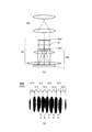
本発明の実施形態を、添付図面に基づいて説明する。図1は、本発明の第1実施形態にかかる光照射装置の構成を概略的に示す図である。図1を参照すると、第1実施形態の光照射装置は、レーザ光源1と、レーザ光源1の直後に配置されたアッテネータ2と、アッテネータ2を経たレーザ光で位相シフタ(光変調素子)3を照明する照明光学系4と、アッテネータ2と照明光学系4との間に配置されたデフォーマブルミラー5と、被処理基板6を保持する基板ステージ7と、位相シフタ3と被処理基板6との間に設けられた結像光学系8とを備えている。
Embodiments of the present invention will be described with reference to the accompanying drawings. FIG. 1 is a diagram schematically showing a configuration of a light irradiation apparatus according to the first embodiment of the present invention. Referring to FIG. 1, a light irradiation apparatus according to the first embodiment includes a
また、第1実施形態の光照射装置は、デフォーマブルミラー5と照明光学系4との間に配置されたハーフミラー(ビームスプリッター)9と、ハーフミラー9で反射されたレーザ光の波面を測定する波面センサユニット10と、波面センサユニット10の出力に基づいてデフォーマブルミラー5を制御する制御部11とを備えている。レーザ光源1として、被結晶化処理体を溶融するエネルギー光線を射出する性能を有する光源、例えばArFエキシマレーザ光源、XeFエキシマレーザ光源、KrFエキシマレーザ光源やXeClエキシマレーザ光源などを用いることができる。
The light irradiation apparatus of the first embodiment measures a half mirror (beam splitter) 9 disposed between the
レーザ光源1から発振されたレーザ光は、光軸に対する傾斜角が可変のアッテネータ2により減衰され、その光強度が調節された後に、デフォーマブルミラー5およびハーフミラー9を介して、照明光学系4に入射する。デフォーマブルミラー5およびハーフミラー9の作用については後述する。図2に示すように、照明光学系4に入射したレーザ光は、テレスコープ(ビームエキスパンダ)4aを介して拡大された後、一対のレンズアレイ4ba,4bbとフィールドレンズ4bcとからなるホモジナイザ4bに入射する。ホモジナイザ4bを介した光束は、位相シフタ3を重畳的に照明する。
The laser light oscillated from the
ホモジナイザ4bにより、照明光学系4に入射したレーザ光について、位相シフタ3上での入射角度に関する均一化が図られる。こうして、照明光学系4は、ほぼ均一な光強度分布を有するレーザ光により位相シフタ3を照射する。位相シフタ3に入射して位相変調されたレーザ光は、結像光学系8を介して、被処理基板6に入射する。ここで、結像光学系8は、位相シフタ3の位相パターン面と被処理基板6とを光学的に共役に配置している。換言すれば、被処理基板6は、位相シフタ3の位相パターン面と光学的に共役な面(結像光学系8の像面)に設定されている。
The
結像光学系8は、第1正レンズ群8aと、第2正レンズ群8bと、これらのレンズ群の間に配置された開口絞り8cを備えている。開口絞り8cの開口部(光透過部)の大きさ(ひいては結像光学系8の像側開口数NA)は、被処理基板6の半導体膜上において所要の光強度分布を発生させるように設定されている。結像光学系8は、屈折型の光学系であってもよいし、反射型の光学系であってもよいし、屈折反射型の光学系であってもよい。
The imaging
被処理基板6は、基板上に、下層絶縁膜、半導体薄膜、上層絶縁膜の順に成膜することにより構成されている。すなわち、被処理基板6は、たとえば液晶ディスプレイ用板ガラスのような透明基板の上に化学気相成長法(CVD)により下地絶縁膜、非単結晶膜例えば非晶質シリコン膜およびキャップ膜が順次形成されたものである。キャップ膜は、例えばSiO2や、SiOxなどである。下地絶縁膜は、非晶質シリコン膜とガラス基板が直接接触してガラスに含まれるNaなどの成分が非晶質シリコン膜に混入するのを防止し、また非晶質シリコン膜の熱が直接ガラス基板に伝熱されるのを防止するために、SiNや、SiNとSiO2の多層膜を使用する。
The
非単結晶シリコン薄膜は、結晶化される半導体膜である。キャップ膜は、非単結晶シリコン薄膜に入射する光ビームの一部により加熱され、この加熱された温度を蓄熱する。この蓄熱効果は、光ビームの入射が遮断されたとき、非単結晶シリコン薄膜の被照射面において高温部が相対的に急速に降温するが、この降温勾配を緩和させ、大粒径の横方向の結晶成長を促進させる。被処理基板6は、真空チャックや静電チャックなどにより基板ステージ7上において予め定められた所定の位置に位置決めされて保持されている。
A non-single crystal silicon thin film is a semiconductor film to be crystallized. The cap film is heated by a part of the light beam incident on the non-single-crystal silicon thin film, and stores the heated temperature. This heat storage effect is that when the incidence of the light beam is interrupted, the high temperature part of the irradiated surface of the non-single-crystal silicon thin film is relatively rapidly cooled, but this temperature gradient is relaxed and the large grain size is reduced in the lateral direction. Promotes crystal growth. The
図1に示す光照射装置では、位相シフタ3を介してその直後に例えば逆ピーク状の光強度分布が形成され、結像光学系8により逆ピーク状の光強度分布の像が被処理基板6の表面上に形成される。その結果、逆ピーク状の光強度分布における光強度の勾配方向に沿って結晶核からラテラル方向に結晶が成長し、大粒径の結晶化半導体膜が生成される。しかしながら、前述したように、レーザ光源の特性の経時的な劣化などに起因して光束の波面の歪みが発生し、この波面の歪みの影響により被処理基板6の表面上において所望の光強度分布を安定的に形成することができなくなる。
In the light irradiation apparatus shown in FIG. 1, for example, a reverse peak light intensity distribution is formed immediately after passing through the
具体的に、波面に歪み(乱れ)が全くない理想的な平面波の光束が照明光学系4中のホモジナイザ4bに入射する場合、ホモジナイザ4bにより形成された複数の小光源の各々からの光も同じく平面状の波面で位相シフタ3を照明し、各小光源からの光が位相シフタ3の直後の平面上に鮮明な像としての所望の光強度分布を形成する。その結果、各小光源からの光は、結像光学系8を介して、被処理基板6の表面上に鮮明な合成像としての所望の光強度分布を形成する。
Specifically, when an ideal plane wave light beam having no distortion (disturbance) in the wavefront is incident on the
一方、波面に歪みのある光束が照明光学系4中のホモジナイザ4bに入射する場合、ホモジナイザ4bにより形成された複数の小光源のうちの少なくとも一部からの光も波面に歪みのある光束で位相シフタ3を照明することになる。このため、ある小光源からの光は位相シフタ3の直後の平面上に鮮明な像としての所望の光強度分布を形成するが、ある小光源からの光は位相シフタ3の直後の平面上に歪んだ像としての光強度分布を形成する。
On the other hand, when a light beam having a wavefront distortion is incident on the
ここで、「歪んだ像」とは、理想的な波面の揃った光でない入射光に起因して発生する、光軸と直交する平面上での像の位置ずれ、光軸方向の像の位置ずれ、像の形状の歪みなどを指す。各小光源からの光は、結像光学系8を介して、被処理基板6の表面上に不鮮明な合成像としての光強度分布を形成する。すなわち、被処理基板6の表面上に形成される光強度分布は、所望の光強度分布に比して、基板6の表面に沿って位置ずれしたり、結像光学系8の光軸方向(フォーカス方向)に位置ずれしたり、形状(プロファイル)が歪んだりし、被処理基板6の表面上において所望の光強度分布を得ることができない。
Here, the “distorted image” refers to an image position shift on a plane orthogonal to the optical axis caused by incident light that is not ideal wavefront aligned light, and the position of the image in the optical axis direction. Displacement, distortion of image shape, etc. Light from each small light source forms a light intensity distribution as a blurred composite image on the surface of the
この問題に対して、レーザ光の周辺を使用することなく中心部のみを使用することにより、すなわちほぼ波面の揃った光束だけを利用することにより所望の光強度分布を得る方法がある。しかしながら、この方法では、利用可能な光エネルギーが大幅に減少するため、スループットが極端に低下してしまう。 In order to solve this problem, there is a method of obtaining a desired light intensity distribution by using only the central portion without using the periphery of the laser beam, that is, by using only a light beam having a substantially uniform wavefront. However, with this method, the available light energy is greatly reduced, resulting in an extremely low throughput.
また、図3に示すように、通常は1段構成であるホモジナイザ(図2参照)を2段構成にすることにより、ほぼ波面の揃った光束だけを利用して所望の光強度分布を得る方法もある。図3の2段構成では、テレスコープ4aを介して拡大された後、第1ホモジナイザ4b(4ba,4bb,4bc)を介して、一対のレンズアレイ4ca,4cbとフィールドレンズ4ccとからなる第2ホモジナイザ4cの入射面を重畳的に照明する。
Further, as shown in FIG. 3, a method of obtaining a desired light intensity distribution by using only a light beam having a substantially uniform wavefront by using a two-stage homogenizer (see FIG. 2), which is normally a one-stage structure. There is also. In the two-stage configuration shown in FIG. 3, after being enlarged through the
さらに、第2ホモジナイザ4cを介した光束は、位相シフタ3を重畳的に照明する。第1ホモジナイザ4bにより、照明光学系4に入射したレーザ光について、位相シフタ3上での入射角度に関する均一化が図られる。また、第2ホモジナイザ4cにより、第1ホモジナイザ4bからの入射角度が均一化されたレーザ光について、位相シフタ3上での面内各位置での光強度に関する均一化が図られる。しかしながら、ホモジナイザを2段構成にする方法においても、利用可能な光エネルギーが大幅に減少するため、スループットが極端に低下してしまう。
Further, the light flux that has passed through the
また、上述の問題はレーザ光源の特性の経時的な劣化が原因であるから、レーザ光源のチューブ(発振用のガス容器)を交換する方法もある。しかしながら、この方法は、レーザ光源のチューブが非常に高価であるため、コスト的な観点から実用的ではない。 In addition, since the above-mentioned problem is caused by the deterioration of the characteristics of the laser light source over time, there is a method of replacing the tube (laser gas container) of the laser light source. However, this method is not practical from the viewpoint of cost because the tube of the laser light source is very expensive.
そこで、第1実施形態では、レーザ光源1と照明光学系4との間にデフォーマブルミラー5とハーフミラー9とを付設し、ハーフミラー9により照明光路から取り出されたレーザ光の波面を波面センサユニット10により測定するとともに、波面センサユニット10の出力に基づいてデフォーマブルミラー5を制御部11により制御する構成を採用している。デフォーマブルミラー5は、波面の歪み(乱れ)を補正するための波面補正光学素子である。ちなみに、市販されているデフォーマブルミラー(Intellite社製)は、薄膜状のアルミニウムからなるミラーの裏面に設けたマトリクス状の高電圧電極間に発生する静電応力を利用して、ミラー平面を局部的に変形させて波面を制御する能動変形ミラーである。
Therefore, in the first embodiment, a
また、波面センサユニット10として、例えばシャック−ハートマン(Shack-Hartmann)型の波面センサを用いることができる。この場合、波面センサユニット10は、光の入射側から順に、例えば保護用シャッター(不図示)と、マイクロレンズアレイ10aと、その集光位置に検出面を有する光検出器(例えばCCD)10bとにより構成される。波面センサユニット10の測定結果を分析してデフォーマブルミラー5の反射面の変形を制御する制御部11として、例えばパーソナルコンピュータを用いることができる。
Moreover, as the
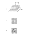
波面センサユニット10のマイクロレンズアレイ10aは、図4(a)に示すように、碁盤の目状に配置された多数の微小レンズ(マイクロレンズ)10aaにより構成されている。したがって、マイクロレンズアレイ10aに入射した光束は多数の微小レンズ10aaにより波面分割され、各微小レンズ10aaを通過した光束はCCD10bの検出面10ba上に集光する。波面センサユニット10に入射する光束の波面に歪みが無く平面状である場合、図4(b)に示すように、碁盤の目状に配置された多数の微小レンズ10aaに対応して、CCD10bの検出面10ba上において多数の集光点が碁盤の目状に形成される。
As shown in FIG. 4A, the
一方、波面センサユニット10に入射する光束の波面に歪みがある場合、図4(c)に示すように、CCD10bの検出面10ba上において1つまたは複数の集光点が波面の歪みに応じて所定位置から位置ずれする。制御部11は、CCD10bの検出面10ba上における1つまたは複数の集光点の所定位置からの位置ずれ情報に基づいて、波面センサユニット10に入射した光束の波面の歪みに関する情報、ひいてはレーザ光源1から射出された光束の波面の歪みに関する情報を計算する。そして、制御部11は、計算により求めた波面の歪み情報に基づいて、この波面の歪みを補正するのに必要なデフォーマルミラー5の所要変形量を計算し、デフォーマルミラー5の反射面の所要領域を所要量だけ変形させる。
On the other hand, when the wavefront of the light beam incident on the
以下、図5のフローチャートを参照して、第1実施形態における波面の調整方法を説明する。第1実施形態の波面調整方法では、先ず、波面の歪みの許容範囲(CCD10bの検出面10ba上における集光点の位置ずれ許容範囲)を制御部11に読み込む(S11)。次に、レーザ光源1をONにしてレーザ光をパルス発振させる(S12)。その後、波面センサユニット10が波面の歪みデータを測定(収集)し(S13)、制御部11は測定された波面の歪み量が許容範囲内か否かを判定する(S14)。判定工程S14において波面の歪み量が許容範囲内であると判定された場合、波面の調整方法は終了する。
Hereinafter, the wavefront adjustment method according to the first embodiment will be described with reference to the flowchart of FIG. In the wavefront adjustment method of the first embodiment, first, an allowable range of wavefront distortion (condensation point allowable range of focus on the detection surface 10ba of the
一方、判定工程S14において波面の歪み量が許容範囲を超えていると判定された場合、制御部11は、波面の歪みを補正するのに必要なデフォーマルミラー5の所要変形量を計算する(S15)。次いで、制御部11は、所要変形量の計算結果に基づいて、デフォーマルミラー5の反射面の所要領域を所要量だけ変形させる(S16)。こうして、レーザ光源1をONにしてレーザ光を再びパルス発振させ(S12)、波面の歪みデータを測定し(S13)、測定された波面の歪み量が許容範囲内か否かを判定する(S14)。
On the other hand, when it is determined in the determination step S14 that the wavefront distortion amount exceeds the allowable range, the
2回目の判定工程S14において波面の歪み量が許容範囲内であると判定された場合、波面の調整方法は終了する。一方、2回目の判定工程S14において波面の歪み量が許容範囲を超えていると判定された場合、計算工程S15、変形工程S16、発振工程S12、測定工程S13、および判定工程S14を繰り返すことにより、波面の適正な調整(補正)を行う。 When it is determined in the second determination step S14 that the wavefront distortion amount is within the allowable range, the wavefront adjustment method ends. On the other hand, when it is determined in the second determination step S14 that the wavefront distortion amount exceeds the allowable range, the calculation step S15, the deformation step S16, the oscillation step S12, the measurement step S13, and the determination step S14 are repeated. Perform proper adjustment (correction) of the wavefront.
こうして、第1実施形態の光照射装置では、レーザ光源1の特性の経時的な劣化などに起因する光束の波面の歪みの影響を抑えて、被処理基板6の表面上において所望の光強度分布を安定的に形成することができ、ひいては所望する粒径の結晶化を安定的に行うことができる。すなわち、たとえばTFTのサイズよりも十分に大きい粒径の結晶を生成し、且つその形成位置を制御してTFTの活性層から結晶粒界を排除することができる。なお、波面調整を行うタイミングとしては、レーザアニールの直前が好ましい。
Thus, in the light irradiation apparatus of the first embodiment, the desired light intensity distribution on the surface of the
第1実施形態では、照明光学系4よりも後段の光学系部分が波面の調整とは無関係である。このため、波面の調整中は、ハーフミラー9と照明光学系4との間に光学系保護のための遮光板を挿入してもよい。また、ハーフミラー9として、50%の透過率および50%の反射率を有するものではなく、例えば透過率が99%で反射率が1%のものなどを用いることができる。ハーフミラー9の透過と反射との比率については様々な変形例が可能であるが、波面センサユニット10のレーザ光耐性を考慮して、CCD10bにおけるレーザフルエンスが10mJ/cm2程度以下となるように、透過率が95%程度で反射率が5%程度のハーフミラー9を用いることが好ましい。
In the first embodiment, the optical system portion subsequent to the illumination
レーザ光源の劣化例を、図17(a)および図17(b)に示す。図17(b)は、1×10⁸ショットの発振後のKrFエキシマレーザ光源からのビームを、図2の照明光学系に類似した構成を有する図17(a)の光学系へ導き、図17(a)の光学系において一対のシリンドリカルレンズアレイ(図2の一対のレンズアレイ4baおよび4bbに対応)4ba’と4bb’との間の光路中に配置された感熱紙40に焼き付けたときに得られたプロファイル(光強度分布)である。図17(b)では、黒色の度合いが強いほど、レーザ強度が高いことを示している。
Examples of degradation of the laser light source are shown in FIGS. 17 (a) and 17 (b). FIG. 17B guides the beam from the KrF excimer laser light source after oscillation of 1 × 10 8 shots to the optical system of FIG. 17A having a configuration similar to that of the illumination optical system of FIG. In the optical system of (a), a pair of cylindrical lens arrays (corresponding to the pair of lens arrays 4ba and 4bb in FIG. 2) obtained when printed on the
感熱紙40の直前に配置されたシリンドリカルレンズアレイ4ba’を構成する各レンズ要素は等間隔に配置され且つ同じ曲率を有するため、図中aで示したすべての間隔は12mmと互いに等しいはずであるが、実測結果ではこれらの間隔が互いに異なっていた。また、本来レーザ光が集光されて達しないはずの領域(図中bで示す領域)に、光が存在していた。これは、レーザ光の波面が乱れており、斜入斜成分が多く存在しているために、領域bが生じたものと考えられる。このように、レーザ光源では、経時劣化によって波面の歪みが顕著になるのである。
Since the lens elements constituting the cylindrical lens array 4ba ′ arranged just before the
図6は、本発明の第2実施形態にかかる光照射装置の構成を概略的に示す図である。第2実施形態は、第1実施形態と類似の構成を有するが、ハーフミラー9および波面センサユニット10が取り除かれている点、基板ステージ7上にビームプロファイラ12が設けられている点、照明光学系4中に可動絞り4dが設けられている点が第1実施形態と相違している。以下、第1実施形態との相違点に着目して、第2実施形態を説明する。
FIG. 6 is a diagram schematically showing a configuration of a light irradiation apparatus according to the second embodiment of the present invention. The second embodiment has a configuration similar to that of the first embodiment, except that the
第2実施形態では、デフォーマブルミラー5を制御するために、ビームプロファイラ12と、ビームプロファイラ12の測定結果を分析する制御部11とを用いる。また、光源を局在化するために、照明光学系4中に設けられた可動絞り4dを用いる。ビームプロファイラ12は、被処理基板6を保持する基板ステージ7上に設けられて、基板6の表面とほぼ同一面に位置決め可能な測定面(観察面)を有する。また、ビームプロファイラ12は、基板6の表面上で互いに直交するX方向およびY方向、並びに結像光学系8の光軸に沿ったZ方向に独立して移動可能であり、1〜200倍程度の拡大倍率を有する。
In the second embodiment, the
ビームプロファイラ12は、不可視レーザ光を検出するセンサとして蛍光性を有する薄膜を備え、この薄膜の変化を測定する蛍光顕微鏡と同等のシステムでもよい。また、ビームプロファイラ12は、UV顕微鏡のように、不可視レーザ光を直接測定するシステムでもよい。具体的に、第2実施形態のビームプロファイラ12として、特開2004−336013号公報に開示されたビームプロファイラを用いることができる。
The
第2実施形態では、位相シフタ3として、レーザ光源1からの射出光の波長の1/2の段差を持つラインアンドスペース型の位相シフタのように単純なものを使用することが好ましい。また、90度角度を変えた方向を見やすくするために、ロの字型の位相シフタでも良い。これは、レーザ光源1の基本的な特性を測定する上で、理論値のわかり易い位相シフタを用いることにより、データ処理の信頼性および高速性が向上するからである。光源を局在化するために用いる可動絞り4dは、図7に示すように照明光学系4中において後側のレンズアレイ4bcの直前に配置され、照明光学系4の瞳を可変的に限定する。
In the second embodiment, it is preferable to use a
なお、図7には、XY平面(光軸に直交する平面)に沿ってレンズが縦横に並んだレンズアレイを示しているが、エキシマレーザのように縦横比が大きいレーザのビーム形状の場合には、X方向のみに屈折力を有するシリンドリカルレンズアレイのセットと、Y方向のみに屈折力を有するシリンドリカルレンズアレイのセットとに分離する方法もある。可動絞り4dは、後側のレンズアレイ4bc中の1つの任意のレンズにのみ光を通過させるように、XY平面に沿って移動可能で且つ開口(光透過部)の大きさを調節可能に構成されている。
FIG. 7 shows a lens array in which lenses are arranged vertically and horizontally along an XY plane (a plane orthogonal to the optical axis). However, in the case of a laser beam shape having a large aspect ratio such as an excimer laser. There is also a method of separating a set of cylindrical lens arrays having refractive power only in the X direction and a set of cylindrical lens arrays having refractive power only in the Y direction. The
以下、図8のフローチャートを参照して、第2実施形態における波面の調整方法を説明する。第2実施形態の波面調整方法では、先ず、ビームプロファイル(位相シフタ3に対応して基板6の表面と同じ高さ位置において得られる光強度分布の二次元データ)の許容範囲を制御部11に読み込む(S21)。次に、ビームプロファイラ12を測定位置へ移動させ(S22)、可動絞り4dの開口をレンズアレイ4bc中の1つのレンズに対応する位置に設定する(S23)。その後、レーザ光源1をONにしてレーザ光をパルス発振させ(S24)、ビームプロファイラ12を用いてビームプロファイル(光強度分布)を測定する(S25)。ビームプロファイラ12の測定結果は、制御部11へ供給される。
Hereinafter, the wavefront adjustment method in the second embodiment will be described with reference to the flowchart of FIG. In the wavefront adjusting method of the second embodiment, first, the
可動絞り4dのXYマッピングに従って開口位置を変化させつつ(すなわち照明光学系4の瞳を変化させつつ)、可動絞り4dの開口の設定工程S23、レーザ光源1のパルス発振工程S24、およびビームプロファイルの測定工程S25を繰り返す。所要回数の測定工程S25が終了すると、制御部11は、ビームプロファイラ12の測定結果に基づいてビームプロファイルの合成計算を行う(S26)。すなわち、制御部11は、ビームプロファイル間の差異を抽出し、その差異と可動絞り4dのXYマッピング(可動絞り4dの開口位置)との相関関係を求める。
While changing the aperture position according to the XY mapping of the
次いで、制御部11は、ビームプロファイル間の差異と可動絞り4dのXYマッピングとの相関関係に基づいて、ビームプロファイルを補正(ひいては波面の歪みを補正)するのに必要なデフォーマルミラー5の所要変形量を計算する(S27)。さらに、制御部11は、工程S27の計算結果に基づいて、デフォーマルミラー5の反射面の所要領域を所要量だけ変形させる(S28)。次に、可動絞り4dを全開状態(可動絞り4dのない状態と光学的に等価な状態)にし(S29)、レーザ光源1をONにしてレーザ光をパルス発振させ(S210)、ビームプロファイラ12を用いてビームプロファイルを測定する(S211)。
Next, the
制御部11は、測定工程S211で得られたビームプロファイルが許容範囲内か否かを判定する(S212)。判定工程S212においてビームプロファイルが許容範囲内であると判定された場合、波面の調整方法は終了する。一方、判定工程S212においてビームプロファイルが許容範囲を超えていると判定された場合、移動工程S22と設定工程S23との間に戻って、工程S23〜工程S212までの作業を繰り返すことにより、波面の適正な調整(補正)を行う。こうして、第2実施形態の光照射装置においても、レーザ光源1の特性の経時的な劣化などに起因する光束の波面の歪みの影響を抑えて、被処理基板6の表面上において所望の光強度分布を安定的に形成することができ、ひいては所望する粒径の結晶化を安定的に行うことができる。
The
図9は、本発明の第3実施形態にかかる光照射装置の構成を概略的に示す図である。第3実施形態は、第1実施形態の特徴的な要部構成と第2実施形態の特徴的な要部構成とを併せ備えている。以下、第1実施形態との相違点および第2実施形態との相違点に着目して、第3実施形態を説明する。第3実施形態の光照射装置では、デフォーマブルミラー5を波面補正光学素子とし、波面計測ユニット5を粗精度の波面調整に用い、細精度の波面調整にビームプロファイラ12を用いる。
FIG. 9 is a diagram schematically showing a configuration of a light irradiation apparatus according to the third embodiment of the present invention. The third embodiment has both the characteristic main part configuration of the first embodiment and the characteristic main part configuration of the second embodiment. Hereinafter, the third embodiment will be described by paying attention to differences from the first embodiment and differences from the second embodiment. In the light irradiation apparatus of the third embodiment, the
以下、図10および図11のフローチャートを参照して、第3実施形態における波面の調整方法を説明する。第3実施形態の波面調整方法では、粗精度の波面調整のために第1実施形態の波面調整方法を適用する。すなわち、第3実施形態の波面調整方法における粗精度の波面調整段階では、図10に示すように、波面の歪みの許容範囲を制御部11に読み込み(S31)、レーザ光源1をONにしてレーザ光をパルス発振させ(S32)、波面センサユニット10が波面の歪みデータを測定し(S33)、測定された波面の歪み量が許容範囲内か否かを判定する(S34)。判定工程S34において波面の歪み量が許容範囲内であると判定された場合、粗精度の波面調整段階は終了する。
Hereinafter, the wavefront adjustment method according to the third embodiment will be described with reference to the flowcharts of FIGS. 10 and 11. In the wavefront adjustment method of the third embodiment, the wavefront adjustment method of the first embodiment is applied for coarse-accuracy wavefront adjustment. That is, in the coarse-accuracy wavefront adjustment stage in the wavefront adjustment method of the third embodiment, as shown in FIG. 10, the allowable range of distortion of the wavefront is read into the control unit 11 (S31), the
一方、判定工程S34において波面の歪み量が許容範囲を超えていると判定された場合、波面の歪みを補正するのに必要なデフォーマルミラー5の所要変形量を計算し(S35)、デフォーマルミラー5の反射面の所要領域を所要量だけ変形させ(S36)、レーザ光源1をONにしてレーザ光を再びパルス発振させ(S32)、波面の歪みデータを測定し(S33)、測定された波面の歪み量が許容範囲内か否かを判定する(S34)。2回目の判定工程S34において波面の歪み量が許容範囲内であると判定された場合、粗精度の波面調整段階は終了する。一方、2回目の判定工程S34において波面の歪み量が許容範囲を超えていると判定された場合、計算工程S35、変形工程S36、発振工程S32、測定工程S33、および判定工程S34を繰り返すことにより、波面の適正な粗精度調整(補正)を行う。
On the other hand, if it is determined in the determination step S34 that the wavefront distortion amount exceeds the allowable range, the required deformation amount of the
次いで、第3実施形態の波面調整方法では、細精度の波面調整のために第2実施形態に類似した波面調整方法を適用する。すなわち、第3実施形態の波面調整方法における細精度の波面調整段階では、図11に示すように、ビームプロファイルの許容範囲を制御部11に読み込み(S31)、ビームプロファイラ12を測定位置へ移動させ(S32)、可動絞り4dの開口を初期位置に設定し(S33)、レーザ光源1をONにしてレーザ光をパルス発振させ(S34)、ビームプロファイラ12を用いてビームプロファイルを測定する(S35)。
Next, in the wavefront adjustment method of the third embodiment, a wavefront adjustment method similar to that of the second embodiment is applied for fine-precision wavefront adjustment. That is, in the fine wavefront adjustment stage in the wavefront adjustment method of the third embodiment, as shown in FIG. 11, the allowable range of the beam profile is read into the control unit 11 (S31), and the
可動絞り4dのXYマッピングに従って開口位置を変化させつつ、設定工程S33、発振工程S34、および測定工程S35を繰り返す。所要回数の測定工程S35が終了すると、ビームプロファイルの合成計算を行い(S36)、デフォーマルミラー5の所要変形量を計算し(S37)、デフォーマルミラー5の反射面の所要領域を所要量だけ変形させ(S38)、可動絞り4dを全開状態にし(S39)、レーザ光源1をONにしてレーザ光をパルス発振させ(S310)、ビームプロファイラ12を用いてビームプロファイルを測定する(S311)。
The setting step S33, the oscillation step S34, and the measurement step S35 are repeated while changing the opening position according to the XY mapping of the
制御部11は、測定工程S311で得られたビームプロファイルが許容範囲内か否かを判定する(S312)。判定工程S312においてビームプロファイルが許容範囲内であると判定された場合、波面の調整方法は終了する。一方、判定工程S312においてビームプロファイルが許容範囲を超えているがその差が比較的小さいと判定された場合、移動工程S32と設定工程S33との間に戻って、工程S33〜工程S312までの作業を繰り返すことにより、波面の適正な細精度調整(補正)を行う。
The
また、判定工程S312においてビームプロファイルが許容範囲を超えており且つその差が比較的大きいと判定された場合、読込工程S31と発振工程S32との間に戻って、上述した粗精度の波面調整および細精度の波面調整を再度行う。こうして、第3実施形態の光照射装置においても、レーザ光源1の特性の経時的な劣化などに起因する光束の波面の歪みの影響を抑えて、被処理基板6の表面上において所望の光強度分布を安定的に形成することができ、ひいては所望する粒径の結晶化を安定的に行うことができる。
If it is determined in the determination step S312 that the beam profile exceeds the allowable range and the difference is relatively large, the process returns between the reading step S31 and the oscillation step S32, and the above-described coarse wavefront adjustment and Perform fine wavefront adjustment again. Thus, also in the light irradiation apparatus of the third embodiment, the desired light intensity on the surface of the
次に、図12(a)乃至(e)を参照して、本実施形態の光照射装置(結晶化装置)を用いて結晶化された領域に電子デバイスを作製する方法を説明する。図12(a)に示すように、絶縁基板80(例えば、アルカリガラス、石英ガラス、プラスチック、ポリイミドなど)の上に、下地膜81(例えば、膜厚50nmのSiNおよび膜厚100nmのSiO2積層膜など)および非晶質半導体膜82(例えば、膜厚50nm〜200nm程度のSi,Ge,SiGeなど)および不図示のキャップ膜82a(例えば、膜厚30nm〜300nmのSiO2膜など)を、化学気相成長法やスパッタ法などを用いて成膜した被処理基板5を準備する。そして、本実施形態にしたがう光照射装置を用いて、非晶質半導体膜82の表面の予め定められた領域に、レーザ光83(例えば、KrFエキシマレーザ光やXeClエキシマレーザ光など)を照射する。
Next, a method for manufacturing an electronic device in a crystallized region using the light irradiation apparatus (crystallization apparatus) of the present embodiment will be described with reference to FIGS. As shown in FIG. 12A, a base film 81 (for example, SiN having a thickness of 50 nm and a SiO 2 layer having a thickness of 100 nm is laminated on an insulating substrate 80 (for example, alkali glass, quartz glass, plastic, polyimide, etc.). Film) and an amorphous semiconductor film 82 (for example, Si, Ge, SiGe, etc. having a film thickness of about 50 nm to 200 nm) and a cap film 82a (for example, a SiO 2 film having a film thickness of 30 nm to 300 nm), for example. A
こうして、図12(b)に示すように、大粒径の結晶を有する多結晶半導体膜または単結晶化半導体膜84が生成される。次に、キャップ膜82aをエッチングにより除去した後、図12(c)に示すように、フォトリソグラフィ技術を用いて多結晶半導体膜または単結晶化半導体膜84を例えば薄膜トランジスタを形成するための領域となる島状の半導体膜85に加工し、表面にゲート絶縁膜86として膜厚20nm〜100nmのSiO2膜を化学気相成長法やスパッタ法などを用いて成膜する。さらに、図12(d)に示すように、ゲート絶縁膜上にゲート電極87(例えば、シリサイドやMoWなど)を形成し、ゲート電極87をマスクにして不純物イオン88(Nチャネルトランジスタの場合にはリン、Pチャネルトランジスタの場合にはホウ素)をイオン注入する。その後、窒素雰囲気でアニール処理(例えば、炉において450°Cで1時間)やレーザによる活性化(レーザ光83を用いる)を行い、不純物を活性化して島状の半導体膜85にソース領域91、ドレイン領域92を形成する。次に、図12(e)に示すように、層間絶縁膜89を成膜してコンタクト穴をあけ、チャネル90でつながるソース91およびドレイン92に接続するソース電極93およびドレイン電極94を形成する。
In this way, as shown in FIG. 12B, a polycrystalline semiconductor film or a single crystallized
以上の工程において、図12(a)および(b)に示す工程で生成された多結晶半導体膜または単結晶化半導体膜84の大粒径結晶の位置に合わせて、チャネル90を形成する。以上の工程により、多結晶トランジスタまたは単結晶化半導体に薄膜トランジスタ(TFT)を形成することができる。こうして製造された多結晶トランジスタまたは単結晶化トランジスタは、液晶表示装置(ディスプレイ)やEL(エレクトロルミネッセンス)ディスプレイなどの駆動回路や、メモリ(SRAMやDRAM)やCPUなどの集積回路などに適用可能である。
In the above process, the
なお、上述の説明では、非単結晶半導体膜に所定の光強度分布を有する光を照射して結晶化半導体膜を生成する結晶化装置に本発明を適用している。しかしながら、これに限定されることなく、一般的に結像光学系を介して所定の光強度分布を所定面に形成する光照射装置、たとえばレーザアニール装置、レーザ結晶化装置、レーザアブレーション加工装置などに対して本発明を適用することができる。 Note that in the above description, the present invention is applied to a crystallization apparatus that generates a crystallized semiconductor film by irradiating a non-single-crystal semiconductor film with light having a predetermined light intensity distribution. However, the present invention is not limited to this, and a light irradiation device that generally forms a predetermined light intensity distribution on a predetermined surface via an imaging optical system, such as a laser annealing device, a laser crystallization device, a laser ablation processing device, etc. The present invention can be applied to.
具体的に、現在一般的に使用されているラインビーム(線状)光学系を用いたレーザアニール装置にも本発明を適用して、波面の歪みの補償、すなわち波面の調整を行うことができる。ラインビームは、矩形レーザビームの短辺を長辺に比して極端に短くしたもので、例えば、0.5mm×10mm〜500mm程度の断面形状を有する。ラインビームレーザアニール装置では、1度から90度の角度で長辺方向と交差する方向にラインビームを相対的に移動させて(スキャンさせて)レーザ照射を行う。スキャンピッチは、典型的には、約20μm/パルスから30μm/パルスである。 Specifically, the present invention can also be applied to a laser annealing apparatus using a line beam (linear) optical system that is generally used at present to compensate for wavefront distortion, that is, to adjust the wavefront. . The line beam is obtained by extremely shortening the short side of the rectangular laser beam as compared with the long side, and has a cross-sectional shape of about 0.5 mm × 10 mm to 500 mm, for example. In the line beam laser annealing apparatus, laser irradiation is performed by relatively moving (scanning) the line beam in a direction intersecting the long side direction at an angle of 1 to 90 degrees. The scan pitch is typically about 20 μm / pulse to 30 μm / pulse.
図13は、ラインビームレーザアニール装置に本発明を適用した第1例を概略的に示す図である。図13の装置は、図1の第1実施形態と類似の構成を有するが、結像光学系8の設置を省略して位相シフタ3の位置に被処理基板6を配置し、且つ照明光学系4と被処理基板6との間にシリンドリカルレンズ21を付設している点が第1実施形態と相違している。図13では、図1の第1実施形態における構成要素と同じ機能を果たす要素に、図1と同じ参照符号を付している。以下、第1実施形態との相違点に着目して、ラインビームレーザアニール装置の第1例を説明する。
FIG. 13 is a diagram schematically showing a first example in which the present invention is applied to a line beam laser annealing apparatus. The apparatus shown in FIG. 13 has a configuration similar to that of the first embodiment shown in FIG. 1, except that the image forming
図13のラインビームレーザアニール装置において、照明光学系4と被処理基板6との間の光路中に付設されたシリンドリカルレンズ21は、図13の紙面に平行な面において正の屈折力を有し、且つ図13の紙面に垂直な面において無屈折力である。したがって、シリンドリカルレンズ21の作用により、図13の紙面に垂直な方向に沿って非常に細長く延びるラインビーム、例えば0.5mm×10mm〜500mm程度の断面形状を有するラインビームが、被処理基板6の表面に照射される。換言すれば、被処理基板6の表面上に所望の断面形状のラインビームが形成されるように、シリンドリカルレンズ21の屈折力が設定されている。
In the line beam laser annealing apparatus of FIG. 13, the
こうして、図13のラインビームレーザアニール装置では、デフォーマブルミラー5の波面調整機能により、レーザ光源1の特性の経時的な劣化などに起因する光束の波面の歪みの影響を抑えることができ、ひいては被処理基板6の表面上において所望の光強度分布を有するラインビームを安定的に形成することができる。図13のラインビームレーザアニール装置の場合、部分的なダイバージェンスの差がラインビームの品質に大きく影響するため、デフォーマブルミラー5による波面の補正は極めて有効であり、像のずれ、ムラ、ボケなどの現象を良好に抑えるだけでなく、被処理基板6への結像に関する焦点深度(DOF)が深くなるという効果がある。
Thus, in the line beam laser annealing apparatus of FIG. 13, the wavefront adjustment function of the
図14は、ラインビームレーザアニール装置に本発明を適用した第2例を概略的に示す図である。図14の装置は、図1の第1実施形態と類似の構成を有するが、結像光学系8に代えて、シリンドリカルレンズ22を含む結像光学系8Aを配置している点が第1実施形態と相違している。図14では、図1の第1実施形態における構成要素と同じ機能を果たす要素に、図1と同じ参照符号を付している。以下、第1実施形態との相違点に着目して、ラインビームレーザアニール装置の第2例を説明する。
FIG. 14 is a diagram schematically showing a second example in which the present invention is applied to a line beam laser annealing apparatus. The apparatus shown in FIG. 14 has a configuration similar to that of the first embodiment shown in FIG. 1 except that an imaging
図14のラインビームレーザアニール装置において、結像光学系8A中に含まれるシリンドリカルレンズ22は、図14の紙面に平行な面において正の屈折力を有し、且つ図14の紙面に垂直な面において無屈折力である。したがって、シリンドリカルレンズ22を含む結像光学系8Aの作用により、図14の紙面に垂直な方向に沿って非常に細長く延びるラインビーム、例えば0.5mm×10mm〜500mm程度の断面形状を有するラインビームが、被処理基板6の表面に照射される。換言すれば、被処理基板6の表面上に所望の断面形状のラインビームが形成されるように、結像光学系8A中のシリンドリカルレンズ22の屈折力が設定されている。
In the line beam laser annealing apparatus of FIG. 14, the
こうして、図14のラインビームレーザアニール装置においても図13の装置と同様に、デフォーマブルミラー5の波面調整機能により、レーザ光源1の特性の経時的な劣化などに起因する光束の波面の歪みの影響を抑えることができ、ひいては被処理基板6の表面上において所望の光強度分布を有するラインビームを安定的に形成することができる。また、図14のラインビームレーザアニール装置の場合においても、部分的なダイバージェンスの差がラインビームの品質に大きく影響するため、デフォーマブルミラー5による波面の補正は極めて有効であり、像のずれ、ムラ、ボケなどの現象を良好に抑えるだけでなく、被処理基板6への結像に関する焦点深度が深くなるという効果がある。
Thus, in the line beam laser annealing apparatus of FIG. 14 as well, in the same way as the apparatus of FIG. 13, the wavefront adjustment function of the
なお、図6の第2実施形態では、図7に示すように照明光学系4中においてレンズアレイ4bcの直前に配置された可動絞り4dを用いて、照明光学系4の瞳を可変的に限定している。具体的に、可動絞り4dは、レンズアレイ4bc中の1つの任意のレンズにのみ光を通過させるように、XY平面に沿って移動可能で且つ開口(光透過部)の大きさを調節可能に構成されている。レンズアレイ4bcは縦横に且つ稠密に配置された多数のレンズにより構成されているので、図15(a)に示すように、レンズアレイ4bcの各レンズに入射する光束は1つの円で模式的に表わされ、レンズアレイ4bcの全体に入射する光束は縦横に且つ規則的に配列された多数の円で模式的に表わされる。
In the second embodiment shown in FIG. 6, the pupil of the illumination
第2実施形態では、図15(b)に示すように、レンズアレイ4bc中の1つの任意のレンズにのみ光を通過させるように、可動絞り4dの開口部(光透過部)が設定される。図15(b)において、黒塗り部分は光の通過を遮る遮光部であり、遮光部中の白抜き部分は光の通過を許容する開口部である。第2実施形態では、可動絞り4dのXYマッピングに従って開口位置を変化させつつビームプロファイラ12を用いてビームプロファイルを測定し、測定されたビームプロファイルが所望の状態でない場合、可動絞り4dの開口位置に対応するデフォーマルミラー5の反射面の所要領域を変形させて波面の歪みを補正する。
In the second embodiment, as shown in FIG. 15B, the opening (light transmitting portion) of the
しかしながら、波面補正光学素子としてのデフォーマルミラー5は必ずしも万能ではなく、レンズアレイ4bc中の1つまたは複数のレンズを通過する光の波面の歪みを補正し切れないことも考えられる。この場合、被処理基板6への光照射に際して、波面の歪みを補正し切れなかった1つまたは複数のレンズを積極的に利用しないことにより、すなわち波面の歪みを補正し切れなかった光束を可動絞り4dで遮ることにより、照明光学系4の瞳を様々な形状に限定して変形照明を行って、被処理基板6上に所望の光強度分布を安定的に形成することができる。
However, the
例えば、第2実施形態の変形例では、図16(a)に示すように照明光学系4の瞳を輪帯状に限定したり、図16(b)に示すように照明光学系4の瞳を正方形の4つの辺に対応する正方環状に限定したり、図16(c)に示すように照明光学系4の瞳を比較的小さい円形状に限定したり、図16(d)に示すように照明光学系4の瞳を比較的小さい正方形状に限定したりする。また、図16(e)に示すように照明光学系4の瞳を4つの円からなる4極状に限定したり、図16(f)に示すように照明光学系4の瞳を4つの正方形からなる4極状に限定したり、図16(g)に示すように照明光学系4の瞳を一方向に細長い矩形状に限定したりする。
For example, in the modification of the second embodiment, the pupil of the illumination
この変形例では、被処理基板6への結像に関する焦点深度や解像度を向上させることができる。しかしながら、可動絞り4dにおける光量損失により被処理基板6上での照度が低下するので、レーザ光源1の出力(レーザパワー)を増大させる必要がある。また、変形照明により被処理基板6への入射光の瞳分布が変わるので、結像特性のシミュレーションを行い、被処理基板6上に形成されるパターンの補正を行う必要がある。
In this modification, the depth of focus and the resolution related to the image formation on the
1 レーザ光源
2 アッテネータ
3 位相シフタ
4 照明光学系
4d 可動絞り
5 デフォーマブルミラー
6 被処理基板
7 基板ステージ
8 結像光学系
10 波面センサユニット
11 制御部
12 ビームプロファイラ
DESCRIPTION OF
Claims (14)
前記レーザ光源からの光に基づいて光変調素子を重畳的に照明するためのホモジナイザを含む照明光学系と、
前記光変調素子により位相変調された光に基づいて所定の光強度分布を所定面に形成する結像光学系と、
前記レーザ光源と前記ホモジナイザとの間に配置されて入射光束の波面を補正して射出する波面補正光学素子と、
前記波面補正光学素子と前記ホモジナイザとの間の光路から光束を取り出して該光束の波面を測定する波面測定部と、
前記波面測定部の出力に基づいて前記波面補正光学素子を制御する制御部とを備えていることを特徴とする光照射装置。 A laser light source;
An illumination optical system including a homogenizer for superimposingly illuminating a light modulation element based on light from the laser light source;
An imaging optical system that forms a predetermined light intensity distribution on a predetermined surface based on the light phase-modulated by the light modulation element;
A wavefront correcting optical element disposed between the laser light source and the homogenizer to correct and emit a wavefront of an incident light beam;
A wavefront measuring unit that takes out a light beam from an optical path between the wavefront correcting optical element and the homogenizer and measures a wavefront of the light beam;
And a control unit that controls the wavefront correcting optical element based on the output of the wavefront measuring unit.
前記レーザ光源からの光に基づいて光変調素子を重畳的に照明するためのホモジナイザを含む照明光学系と、
前記光変調素子により位相変調された光に基づいて所定の光強度分布を所定面に形成する結像光学系と、
前記レーザ光源と前記ホモジナイザとの間に配置されて入射光束の波面を補正して射出する波面補正光学素子と、
前記照明光学系の瞳を可変的に限定する可動絞りと、
前記所定面に形成される光強度分布を測定するビームプロファイラと、
前記可動絞りおよび前記波面補正光学素子を制御する制御部とを備え、
前記制御部は、前記照明光学系の瞳の変化に応じて測定される光強度分布の情報に基づいて前記波面補正光学素子を制御することを特徴とする光照射装置。 A laser light source;
An illumination optical system including a homogenizer for superimposingly illuminating a light modulation element based on light from the laser light source;
An imaging optical system that forms a predetermined light intensity distribution on a predetermined surface based on the light phase-modulated by the light modulation element;
A wavefront correcting optical element disposed between the laser light source and the homogenizer to correct and emit a wavefront of an incident light beam;
A movable diaphragm that variably limits the pupil of the illumination optical system;
A beam profiler for measuring the light intensity distribution formed on the predetermined surface;
A control unit for controlling the movable diaphragm and the wavefront correcting optical element,
The light irradiation apparatus, wherein the control unit controls the wavefront correction optical element based on information on a light intensity distribution measured according to a change in a pupil of the illumination optical system.
前記ホモジナイザよりも光源側の光路から取り出した光束の波面を測定する波面測定工程と、
前記波面測定工程で得られた測定結果に基づいて、前記ホモジナイザへ入射する光束の波面を補正する波面補正工程とを含むことを特徴とする調整方法。 An illumination optical system including a homogenizer illuminates the light modulation element with light from a laser light source, and forms an image on the predetermined surface by the imaging optical system with the light modulated in phase by the light modulation element. A method of adjusting a light irradiation device that forms a predetermined light intensity distribution in
A wavefront measuring step for measuring a wavefront of a light beam extracted from the optical path on the light source side of the homogenizer;
And a wavefront correcting step of correcting a wavefront of a light beam incident on the homogenizer based on a measurement result obtained in the wavefront measuring step.
前記照明光学系の瞳を可変的に限定する限定工程と、
前記所定面に形成される光強度分布を測定する分布測定工程と、
前記照明光学系の瞳の変化に応じて前記分布測定工程で得られた測定結果に基づいて、前記ホモジナイザへ入射する光束の波面を補正する波面補正工程とを含むことを特徴とする調整方法。 An illumination optical system including a homogenizer illuminates the light modulation element with light from a laser light source, and forms an image on the predetermined surface by the imaging optical system with the light modulated in phase by the light modulation element. A method of adjusting a light irradiation device that forms a predetermined light intensity distribution in
A limiting step of variably limiting the pupil of the illumination optical system;
A distribution measuring step for measuring a light intensity distribution formed on the predetermined surface;
And a wavefront correction step of correcting a wavefront of a light beam incident on the homogenizer based on a measurement result obtained in the distribution measurement step according to a change in a pupil of the illumination optical system.
請求項8に記載の調整方法を用いて前記ホモジナイザへ入射する光束の波面を粗精度で補正する粗精度補正工程と、
請求項9に記載の調整方法を用いて前記ホモジナイザへ入射する光束の波面を細精度で補正する細精度補正工程とを含むことを特徴とする調整方法。 An illumination optical system including a homogenizer illuminates the light modulation element with light from a laser light source, and forms an image on the predetermined surface by the imaging optical system with the light modulated in phase by the light modulation element. A method of adjusting a light irradiation device that forms a predetermined light intensity distribution in
A coarse accuracy correction step of correcting the wavefront of the light beam incident on the homogenizer with coarse accuracy using the adjustment method according to claim 8;
An adjustment method comprising: a fine precision correction step of finely correcting a wavefront of a light beam incident on the homogenizer using the adjustment method according to claim 9.
Priority Applications (1)
| Application Number | Priority Date | Filing Date | Title |
|---|---|---|---|
| JP2006203587A JP2007150245A (en) | 2005-11-04 | 2006-07-26 | Light irradiation device, method of regulating light irradiation device, crystallization apparatus, crystallization method, and device |
Applications Claiming Priority (2)
| Application Number | Priority Date | Filing Date | Title |
|---|---|---|---|
| JP2005320623 | 2005-11-04 | ||
| JP2006203587A JP2007150245A (en) | 2005-11-04 | 2006-07-26 | Light irradiation device, method of regulating light irradiation device, crystallization apparatus, crystallization method, and device |
Publications (2)
| Publication Number | Publication Date |
|---|---|
| JP2007150245A true JP2007150245A (en) | 2007-06-14 |
| JP2007150245A5 JP2007150245A5 (en) | 2008-04-17 |
Family
ID=38211223
Family Applications (1)
| Application Number | Title | Priority Date | Filing Date |
|---|---|---|---|
| JP2006203587A Abandoned JP2007150245A (en) | 2005-11-04 | 2006-07-26 | Light irradiation device, method of regulating light irradiation device, crystallization apparatus, crystallization method, and device |
Country Status (1)
| Country | Link |
|---|---|
| JP (1) | JP2007150245A (en) |
Cited By (3)
| Publication number | Priority date | Publication date | Assignee | Title |
|---|---|---|---|---|
| JP2009043788A (en) * | 2007-08-06 | 2009-02-26 | Ulvac Japan Ltd | Laser annealing device, and laser annealing method |
| WO2018066172A1 (en) * | 2016-10-04 | 2018-04-12 | 株式会社日本製鋼所 | Laser irradiation device, method for manufacturing semiconductor device, and method for operating laser irradiation device |
| KR20200024638A (en) * | 2018-08-28 | 2020-03-09 | 국방과학연구소 | Optical communication systems with improved link availability |
-
2006
- 2006-07-26 JP JP2006203587A patent/JP2007150245A/en not_active Abandoned
Cited By (7)
| Publication number | Priority date | Publication date | Assignee | Title |
|---|---|---|---|---|
| JP2009043788A (en) * | 2007-08-06 | 2009-02-26 | Ulvac Japan Ltd | Laser annealing device, and laser annealing method |
| WO2018066172A1 (en) * | 2016-10-04 | 2018-04-12 | 株式会社日本製鋼所 | Laser irradiation device, method for manufacturing semiconductor device, and method for operating laser irradiation device |
| JP2018060888A (en) * | 2016-10-04 | 2018-04-12 | 株式会社日本製鋼所 | Laser irradiation device, method for manufacturing semiconductor device, and method for operating laser irradiation device |
| US10658185B2 (en) | 2016-10-04 | 2020-05-19 | The Japan Steel Works, Ltd. | Laser irradiation apparatus, method for manufacturing semiconductor device, and method for operating laser irradiation apparatus |
| TWI716608B (en) * | 2016-10-04 | 2021-01-21 | 日商日本製鋼所股份有限公司 | Laser irradiation device, method of manufacturing semiconductor device, and operation method of laser irradiation device |
| KR20200024638A (en) * | 2018-08-28 | 2020-03-09 | 국방과학연구소 | Optical communication systems with improved link availability |
| KR102171779B1 (en) * | 2018-08-28 | 2020-10-29 | 국방과학연구소 | Optical communication systems with improved link availability |
Similar Documents
| Publication | Publication Date | Title |
|---|---|---|
| JP5231234B2 (en) | System for generating laser light shaped as a line beam | |
| KR101167324B1 (en) | Laser thin film poly-silicon annealing optical system | |
| JP4413569B2 (en) | Display panel manufacturing method and display panel | |
| JP6471379B2 (en) | Thin film transistor, thin film transistor manufacturing method, and laser annealing apparatus | |
| US7317179B2 (en) | Systems and methods to shape laser light as a homogeneous line beam for interaction with a film deposited on a substrate | |
| JP4956987B2 (en) | Laser crystallization apparatus and crystallization method | |
| KR20060047591A (en) | Laser crystallization apparatus and laser crystallization method | |
| KR20060126665A (en) | Laser thin film poly-silicon annealing system | |
| US8052791B2 (en) | Crystallization apparatus, crystallization method, phase modulation element, device and display apparatus | |
| JP2008124149A (en) | Optical device, and crystallization equipment | |
| KR20040002803A (en) | Crystallization Apparatus, Optical Member for Use in Crystallization Apparatus, Crystallization Method, Manufacturing Method of Thin Film Transistor, and Manufacturing Method of Matrix Circuit Substrate of Display | |
| JP2004311906A (en) | Laser processing device and laser processing method | |
| JP2007214388A (en) | Crystallizing device and positioning stage | |
| JP2005210061A (en) | Apparatus and method for crystallization, method for manufacturing electronic device, electronic device, and optical modulation element | |
| JP2008288508A (en) | Crystallization device and crystallization method | |
| JP2007150245A (en) | Light irradiation device, method of regulating light irradiation device, crystallization apparatus, crystallization method, and device | |
| JP2008159836A (en) | Laser annealing method and laser annealing apparatus | |
| US20090057764A1 (en) | Thin film transistor and display apparatus | |
| JP4567474B2 (en) | Light irradiation apparatus, crystallization apparatus, and crystallization method | |
| JP4652707B2 (en) | Crystallization apparatus, crystallization method, phase modulation element, and device | |
| TWI328487B (en) | Systems and methods to shape laser light as a line beam for interaction with a substrate having surface variations | |
| JP4763983B2 (en) | Light modulation element, crystallization apparatus, crystallization method, thin film semiconductor substrate manufacturing apparatus, thin film semiconductor substrate manufacturing method, thin film semiconductor device, thin film semiconductor device manufacturing method, display device, and phase shifter | |
| JP2007129073A (en) | Light irradiation device, crystallization apparatus and method, and device | |
| WO2020184153A1 (en) | Laser annealing device | |
| WO2007048506A1 (en) | Optical device for generating a line focus on a surface |
Legal Events
| Date | Code | Title | Description |
|---|---|---|---|
| A521 | Written amendment |
Free format text: JAPANESE INTERMEDIATE CODE: A523 Effective date: 20080305 |
|
| A621 | Written request for application examination |
Free format text: JAPANESE INTERMEDIATE CODE: A621 Effective date: 20080305 |
|
| A977 | Report on retrieval |
Free format text: JAPANESE INTERMEDIATE CODE: A971007 Effective date: 20090910 |
|
| A762 | Written abandonment of application |
Free format text: JAPANESE INTERMEDIATE CODE: A762 Effective date: 20091102 |