JP2007141200A - Data processor - Google Patents
Data processor Download PDFInfo
- Publication number
- JP2007141200A JP2007141200A JP2006082566A JP2006082566A JP2007141200A JP 2007141200 A JP2007141200 A JP 2007141200A JP 2006082566 A JP2006082566 A JP 2006082566A JP 2006082566 A JP2006082566 A JP 2006082566A JP 2007141200 A JP2007141200 A JP 2007141200A
- Authority
- JP
- Japan
- Prior art keywords
- cpu
- break
- clock signal
- debug
- clock
- Prior art date
- Legal status (The legal status is an assumption and is not a legal conclusion. Google has not performed a legal analysis and makes no representation as to the accuracy of the status listed.)
- Pending
Links
Images


Landscapes
- Debugging And Monitoring (AREA)
Abstract
Description
本発明は、複数のCPU(中央処理装置)を搭載するデータ処理装置、さらにはそれにおけるデバッグ技術に関し、例えばマイクロコンピュータに適用して有効な技術に関する。 The present invention relates to a data processing apparatus equipped with a plurality of CPUs (central processing units), and further to a debugging technique therefor, for example, a technique effective when applied to a microcomputer.
複数のCPUを搭載するデータ処理装置の一例とされるマイクロコンピュータのデバッグ技術としては、例えば搭載されているプロセッサの個数と同数のデバッグ用端子群を設け、各端子群毎に、それぞれ対応するデバッグ装置を接続することにより、各プロセッサのデバッグを個別的に行う技術が知られている(例えば特許文献1の図4参照)。かかる構成においては、搭載されるCPUの個数が増えると、それに応じてデバッグ用端子やデバッグ回路を追加する必要があるため、コストの上昇を余儀なくされる。 As a debugging technique for a microcomputer, which is an example of a data processing apparatus equipped with a plurality of CPUs, for example, the same number of debugging terminal groups as the number of installed processors are provided, and each terminal group has a corresponding debugging function. A technique for individually debugging each processor by connecting devices is known (see, for example, FIG. 4 of Patent Document 1). In such a configuration, as the number of CPUs to be mounted increases, it is necessary to add a debugging terminal and a debugging circuit accordingly, so that the cost is inevitably increased.
これに対して、搭載されている複数のCPUによってデバッグ用端子を共有する技術が知られている(例えば特許文献1の図1、特許文献2の図1参照)。第1CPUのデバッグ回路と、第2CPUのデバッグ回路と、デバッグ用端子を共有するため、選択接続手段が設けられ、この選択接続手段によって、上記デバッグ用端子が、第1CPUのデバッグ回路と、第2CPUのデバッグ回路とに選択的に結合されるようになっている。この場合、CPUの個数が増えても、デバッグ用端子やデバッグ回路を追加する必要はない。しかしながら、第1CPUのデバッグ回路と第2CPUのデバッグ回路とは、接続されるCPUを個別にデバッグ制御するように構成されているため第1CPUと第2CPUとの統合的なシステム動作の試験は困難とされる。
On the other hand, a technique for sharing a debugging terminal by a plurality of mounted CPUs is known (for example, see FIG. 1 of
これに対して、マルチプロセッサ処理装置におけるプロセッサの個々の動作状態を保持して統合的なシステム全体の動作状態を保持するようにした技術が知られている(例えば特許文献3参照)。それによれば、ブレーク条件の成立やその他の要因で任意のプロセッサの動作状態が通常走行状態から試験走行状態に変化したことを検出すると、プロセッサの動作状態に応じてシステム状態が遷移される。このとき、必要に応じて、動作状態が変化しなかった他のプロセッサの動作状態が通常走行状態から試験走行状態に遷移され、動作状態が試験走行状態となっているものについての動作試験が制御される。 On the other hand, a technique is known in which individual operation states of processors in a multiprocessor processing apparatus are held to hold the operation state of the entire integrated system (see, for example, Patent Document 3). According to this, when it is detected that the operation state of an arbitrary processor has changed from the normal running state to the test running state due to the establishment of a break condition or other factors, the system state is transitioned according to the operating state of the processor. At this time, if necessary, the operation state of the other processor whose operation state has not changed is changed from the normal running state to the test running state, and the operation test for the operation state in the test running state is controlled. Is done.
複数のCPUを含むマイクロプロセッサのシステムデバッグにおいては、デバッグ効率の向上のため、上記複数のCPUでデバッグ対象となるユーザプログラム(以下、ユーザプログラム)が実行されている場合において、所定のブレーク条件が成立した場合に、上記複数のCPUを同時にブレークさせる機能(同時ブレーク機能)や、上記ブレーク後に複数のCPUで再びユーザプログラムの実行が同時に開始される機能(同時実行機能)の搭載が望まれる。 In system debugging of a microprocessor including a plurality of CPUs, in order to improve debugging efficiency, when a user program to be debugged (hereinafter referred to as a user program) is executed by the plurality of CPUs, a predetermined break condition is set. When established, it is desired to mount a function for simultaneously breaking the plurality of CPUs (simultaneous break function) and a function for simultaneously starting execution of the user program again by the plurality of CPUs after the break (simultaneous execution function).
上記同時ブレーク機能や同時実行機能は、ソフトウェアあるいはハードウェアにより実現することが考えられる。上記同時ブレーク機能や同時実行機能を、エミュレータに結合されたパーソナルコンピュータ上でソフトウェアにより実現する場合について本願発明者らが検討したところ、上記複数のCPU間で上記同時ブレークや同時実行に数ミリ秒のオーダーで時間差を生ずることが見いだされた。また、上記同時ブレーク機能や同時実行機能をエミュレータ上のハードウェアにより実現した場合には、上記複数のCPU間で上記同時ブレークや同時実行に数マイクロ秒のオーダーで時間差を生ずることが見出された。このような時間差は、複数のCPU間でブレーク機能がもしくは同時実行に移るまでに多数の命令の実行ずれを生じ、上記複数のCPU間で同期してデバッグ動作されているとは言い難い。命令の実行ずれが数命令以下であれば同期動作しているといって差し支えない。 The simultaneous break function and the simultaneous execution function can be realized by software or hardware. The inventors of the present invention have examined the case where the simultaneous break function and the simultaneous execution function are realized by software on a personal computer coupled to an emulator. It has been found that there is a time difference in the order of. In addition, when the simultaneous break function and the simultaneous execution function are realized by hardware on an emulator, it is found that a time difference occurs in the order of several microseconds between the multiple CPUs in the simultaneous break and simultaneous execution. It was. Such a time difference causes a shift in the execution of a large number of instructions before the break function is started or the simultaneous execution is performed among a plurality of CPUs, and it is difficult to say that a debugging operation is performed synchronously among the plurality of CPUs. If the instruction deviation is less than several instructions, it can be said that the operation is synchronous.
上記特許文献3には、複数のCPUが協調して行う動作をデバッグする場合、ある条件でプロセッサを同時に停止させるなど、複数のCPU間でデバッグ動作を同期させることの必要性について記載されているものの、同時ブレークを可能とするための具体的な構成や、実際にどの程度の同時性が保証されるかは明らかにされていない。 Patent Document 3 describes the necessity of synchronizing debugging operations among a plurality of CPUs such as simultaneously stopping processors under certain conditions when debugging operations performed by a plurality of CPUs in cooperation. However, the specific configuration for enabling simultaneous breaks and how much simultaneity is actually guaranteed are not clarified.
ブレーク条件成立に応じて上記複数のCPUを選択的に、あるいは同時にブレークさせる必要があるが、上記特許文献3の記載技術によれば、条件成立によるブレークにおいて、ブレーク条件が成立したCPUが必ずブレークされてしまい、ブレーク条件が成立したCPUをブレークさせずに、それ以外のCPUをブレークさせることについては記載されていない。 Although it is necessary to break the plurality of CPUs selectively or simultaneously according to the establishment of the break condition, according to the technique described in Patent Document 3, the CPU that satisfies the break condition is always in a break when the condition is satisfied. Thus, there is no description about breaking other CPUs without breaking the CPUs that satisfy the break condition.
上記特許文献3の記載技術によれば、何れかのCPUでブレーク条件が成立した場合に、先ずそのCPUがブレークされ、それがデバッグ回路で認識されてから別のCPUがブレークされるようになっており、条件が成立した観測対象のCPUを含めた任意の数のCPUを選択的に、あるいは複数同時にブレークさせることについては記載されていない。 According to the technique described in Patent Document 3, when a break condition is established in any CPU, the CPU is first broken, and after that is recognized by the debug circuit, another CPU is broken. However, there is no description of selectively breaking any number of CPUs including the CPUs to be observed that satisfy the condition or a plurality of CPUs simultaneously.
上記特許文献3の記載技術によれば、何れかのCPUが外部要因によりブレークされ、それがデバッグ支援回路で認識されてから別のCPUがブレークされるようになっており、外部要因に応じて、複数のCPUを同時にブレークさせることについては記載されていない。 According to the technology described in Patent Document 3, one of the CPUs breaks due to an external factor, and after that is recognized by the debug support circuit, another CPU breaks. There is no description about simultaneously breaking a plurality of CPUs.
また、上記特許文献3の記載技術によれば、何れかのCPUがブレークされた後、ユーザプログラムの実行へ復帰する際の任意の数のCPUに対する実行の制御については記載されていない。 Further, according to the technique described in Patent Document 3, the execution control for an arbitrary number of CPUs when returning to the execution of the user program after any CPU is broken is not described.
また、複数のCPUを含むマイクロプロセッサのシステムデバッグにおいて、デバッグ効率の向上のためには、上記複数のCPUの動作についてのトレース情報を円滑にトレースすることが重要とされる。これについて本願発明者が検討したところ、マイクロプロセッサのシステムデバッグにおいては、以下の理由により、円滑なトレースが困難とされることが見いだされた。 In system debugging of a microprocessor including a plurality of CPUs, it is important to smoothly trace the trace information about the operations of the plurality of CPUs in order to improve debugging efficiency. The inventors of the present invention have examined this, and it has been found that smooth tracing is difficult in the system debugging of the microprocessor for the following reason.
互いに周波数が異なる複数のクロック信号が用いられるマイクロプロセッサにおいては、CPUに供給されるクロック信号の周波数が最も高くされるため、デバッグ回路においては、上記CPUに供給されるクロック信号を用いてトレースすることにより、CPUバスやシステムバスの状態を漏れなくトレースすることができた。 In a microprocessor in which a plurality of clock signals having different frequencies are used, the frequency of the clock signal supplied to the CPU is the highest. Therefore, in the debug circuit, tracing is performed using the clock signal supplied to the CPU. Thus, the state of the CPU bus and the system bus can be traced without omission.
しかしながら、複数のCPUを含むマイクロプロセッサのシステムデバッグにおいては、複数のCPU間の動作速度が異なったり、しかもシステムによってはその動作速度が動的に変更される場合もある。かかる場合において、トレース時におけるデバッグ回路のクロック信号の周波数を決定することができないため、円滑なトレースが困難とされる。 However, in system debugging of a microprocessor including a plurality of CPUs, the operation speed between the plurality of CPUs is different, and the operation speed may be dynamically changed depending on the system. In such a case, since the frequency of the clock signal of the debug circuit at the time of tracing cannot be determined, smooth tracing is difficult.
本発明の目的は、複数のCPUを含むデータ処理装置においてシステムデバッグの効率向上を図るための技術を提供することにある。 An object of the present invention is to provide a technique for improving the efficiency of system debugging in a data processing apparatus including a plurality of CPUs.
本発明の別の目的は、複数のCPUを含むデータ処理装置において、ブレーク条件が成立した場合に任意のCPUを選択的にブレーク可能な技術を提供することにある。 Another object of the present invention is to provide a technique capable of selectively breaking an arbitrary CPU when a break condition is satisfied in a data processing apparatus including a plurality of CPUs.
本発明の別の目的は、複数のCPUを含むデータ処理装置において、ブレーク後にユーザプログラムを同時に実行させるための技術を提供する。 Another object of the present invention is to provide a technique for simultaneously executing a user program after a break in a data processing apparatus including a plurality of CPUs.
本発明の別の目的は、複数のCPUを含むデータ処理装置において、円滑なトレースを可能とするための技術を提供することにある。 Another object of the present invention is to provide a technique for enabling smooth tracing in a data processing apparatus including a plurality of CPUs.
本発明の前記並びにその他の目的と新規な特徴は本明細書の記述及び添付図面から明らかになるであろう。 The above and other objects and novel features of the present invention will be apparent from the description of this specification and the accompanying drawings.
本願において開示される発明のうち代表的なものの概要を簡単に説明すれば下記の通りである。 The following is a brief description of an outline of typical inventions disclosed in the present application.
〔1〕すなわち、それぞれユーザプログラムの実行停止要求に応じてユーザプログラムの実行を停止させる停止制御手段と、ユーザプログラムの実行再開を許可または抑止させる再開制御手段とを有する複数のCPUと、上記複数のCPUで実行されるユーザプログラムのデバッグを可能とするデバッグ回路とを含むデータ処理装置において、上記デバッグ回路内に、上記複数のCPU分の上記再開制御手段に対しユーザプログラムの実行再開を同時に許可する同時実行モードを有する実行制御回路を設ける。 [1] That is, a plurality of CPUs each having stop control means for stopping execution of a user program in response to a request for stopping execution of the user program, and restart control means for permitting or inhibiting execution of the user program; In a data processing apparatus including a debug circuit that enables debugging of a user program executed by a CPU of the CPU, the restart control unit for the plurality of CPUs is allowed to resume execution of the user program simultaneously in the debug circuit. An execution control circuit having a simultaneous execution mode is provided.
上記〔1〕記載の手段によれば、実行制御回路は、上記同時実行モードを有することから、ブレークされた状態からの復帰によるユーザプログラム実行のタイミング的なずれを上記複数のCPU間で最小限に抑えることができ、このことが、複数のCPUを含むデータ処理装置のシステムデバッグにおけるデバッグ効率向上を達成する。 According to the means described in [1] above, since the execution control circuit has the simultaneous execution mode, the timing shift of the user program execution due to the return from the break state is minimized among the plurality of CPUs. This achieves improved debugging efficiency in system debugging of a data processing apparatus including a plurality of CPUs.
〔2〕また、それぞれユーザプログラムの実行停止要求に応じてユーザプログラムの実行を停止させる停止制御手段と、ユーザプログラムの実行再開を許可または抑止させる再開制御手段を有する複数のCPUと、上記複数のCPUで実行されるユーザプログラムのデバッグを可能とするデバッグ回路とを含むデータ処理装置において、上記デバッグ回路内に、上記複数のCPUの何れかにおいてブレーク条件が成立した場合に、それに呼応して、上記複数のCPU分の上記停止制御手段に対しユーザプログラムの実行停止要求を同時に行う同時ブレークモードを有するブレーク制御回路と、上記複数のCPU分の上記再開制御手段に対しユーザプログラムの実行再開を同時に許可する同時実行モードを有する実行制御回路とを設ける。 [2] In addition, a plurality of CPUs each having a stop control unit that stops execution of the user program in response to an execution stop request for the user program, a restart control unit that allows or suppresses execution restart of the user program, In a data processing apparatus including a debugging circuit that enables debugging of a user program executed by the CPU, when a break condition is established in any of the plurality of CPUs in the debugging circuit, in response, A break control circuit having a simultaneous break mode for simultaneously requesting stop of execution of the user program to the stop control means for the plurality of CPUs, and resuming execution of the user program simultaneously for the restart control means for the plurality of CPUs. And an execution control circuit having a concurrent execution mode to be permitted.
上記〔2〕記載の手段によれば、ブレーク制御回路は、上記同時ブレークモードを有することから、上記複数のCPUの何れかにおいてブレーク条件が成立した後における上記複数のCPU間での命令実行のずれを最小限に抑えることができる。さらに、実行制御回路、同時実行モードを有することから、ブレークされた状態からの復帰によるユーザプログラム実行のタイミング的なずれを上記複数のCPU間で最小限に抑えることができる。このことが、複数のCPUを含むデータ処理装置のシステムデバッグにおけるデバッグ効率向上を達成する。 According to the means described in [2] above, since the break control circuit has the simultaneous break mode, instruction execution between the plurality of CPUs after a break condition is established in any one of the plurality of CPUs. Deviation can be minimized. Further, since the execution control circuit and the simultaneous execution mode are provided, the timing shift of the user program execution due to the return from the broken state can be minimized among the plurality of CPUs. This achieves improved debugging efficiency in system debugging of a data processing apparatus including a plurality of CPUs.
〔3〕このとき、外部端子数の増大を抑えるため、上記デバッグ回路は、上記複数のCPUで実行されるユーザプログラムのデバッグ結果を、共通の複数のデバッグ端子から外部出力するためのデバッグインタフェースを設けると良い。 [3] At this time, in order to suppress an increase in the number of external terminals, the debug circuit provides a debug interface for externally outputting the debug results of the user program executed by the plurality of CPUs from a plurality of common debug terminals. It is good to provide.
〔4〕ユーザプログラムの構成によっては、複数のCPUの何れかを個別的にブレークしたい場合があり、かかる場合を考慮すれば、上記ブレーク制御回路において、上記複数のCPUの何れかにおいてブレーク条件が成立した場合に、それに呼応して上記複数のCPUの何れか一つを個別的又は何れか任意の数を個別的にブレーク可能な個別的ブレークモードを含めるのが良い。 [4] Depending on the configuration of the user program, it may be desired to individually break one of the plurality of CPUs. In consideration of such a case, in the break control circuit, there is a break condition in one of the plurality of CPUs. When established, it is preferable to include an individual break mode in which any one of the plurality of CPUs can be individually broken or any arbitrary number can be individually broken.
〔5〕ユーザプログラムの構成によっては、ブレーク状態からの復帰によるユーザプログラム実行開始を上記CPU毎に個別的に制御したい場合があり、かかる場合を考慮すれば、上記実行制御回路には、ブレーク状態からの復帰によるユーザプログラム実行開始を上記CPU毎に個別的に制御可能な個別的実行モードを含めるのが良い。 [5] Depending on the configuration of the user program, there is a case where it is desired to individually control the start of user program execution by returning from the break state for each CPU. In consideration of such a case, the execution control circuit includes a break state. It is preferable to include an individual execution mode capable of individually controlling the start of user program execution by returning from each CPU.
〔6〕上記ブレーク制御回路は、所定のブレーク要因に応じてブレーク要求を形成するためのブレーク要求回路と、設定されたブレーク条件とブレーク要因に応じて上記ブレーク要求をマスクすることによって、上記複数のCPUの中からブレーク対象とされるCPUに対してのみユーザプログラムの実行停止を要求することが可能なブレーク要求マスク回路とを含んで構成することができる。 [6] The break control circuit includes a break request circuit for forming a break request according to a predetermined break factor, and masking the break request according to a set break condition and a break factor. A break request mask circuit capable of requesting only the CPU targeted for a break from the CPUs to stop the execution of the user program can be configured.
〔7〕上記ブレーク要求回路は、それぞれブレーク条件を設定可能な複数のブレーク条件レジスタを更に含み、上記ブレーク条件設定レジスタの設定条件に従って、対応するCPUに対するブレーク制御を行うように構成することができる。 [7] The break request circuit may further include a plurality of break condition registers each capable of setting a break condition, and may be configured to perform break control for the corresponding CPU according to the setting conditions of the break condition setting register. .
〔8〕上記ブレーク条件レジスタは、観測対象となるCPUを設定可能な第1フィールドと、上記第1フィールドに設定されたCPUについてのブレーク条件を設定可能な第2フィールドとを含んで構成することができる。 [8] The break condition register includes a first field capable of setting a CPU to be observed and a second field capable of setting a break condition for the CPU set in the first field. Can do.
〔9〕上記ブレーク制御回路は、上記複数のブレーク条件の組み合わせによるシーケンシャルブレークの条件を設定可能とするシーケンシャルブレーク条件レジスタを更に含み、上記シーケンシャルブレーク条件レジスタの設定情報に基づいてブレーク条件を判定して、対応するCPUに対してユーザプログラムの実行停止を要求することが可能となるように構成することができる。 [9] The break control circuit further includes a sequential break condition register capable of setting a sequential break condition based on a combination of the plurality of break conditions, and determines a break condition based on setting information of the sequential break condition register. Thus, the CPU can be configured to request the corresponding CPU to stop executing the user program.
〔10〕上記デバッグインタフェースは、上記複数のデバッグ端子からの入力を受けて、複数のCPUに対して個別的にリセット要求を行うことを可能とするリセット制御回路を含んで構成することができる。それによれば、上記デバッグインタフェースは、個別的に複数のCPUに対してリセット要求を制御する機能を有することから、上記複数のCPUの中から任意の数のCPUの状態をリセットすることができる。 [10] The debug interface may include a reset control circuit that receives inputs from the plurality of debug terminals and can individually make a reset request to a plurality of CPUs. According to this, since the debug interface has a function of individually controlling a reset request to a plurality of CPUs, it is possible to reset the state of an arbitrary number of CPUs from the plurality of CPUs.
〔11〕上記デバッグインタフェースは、上記複数のデバッグ端子からの入力を受けて設定可能な、複数のCPUにしてリセット要求の制御を行うためのリセット制御レジスタを含み、上記リセット信号制御レジスタの設定値に従って、複数のCPUそれぞれに対して個別的にリセット要求を行うことを可能となるよう構成することができる。 [11] The debug interface includes a reset control register for controlling a reset request by a plurality of CPUs, which can be set by receiving inputs from the plurality of debug terminals, and a set value of the reset signal control register Accordingly, it is possible to make it possible to individually make a reset request to each of the plurality of CPUs.
〔12〕上記実行制御回路は、上記同時実行モードと上記個別的実行モードの制御を可能とする同時実行制御レジスタを含み、同時実行制御レジスタの設定と上記複数のCPUの状態に従って、それぞれのCPUに対してユーザプログラムの実行再開を要求する制御信号生成回路を含んで構成することができる。 [12] The execution control circuit includes a simultaneous execution control register that enables control of the simultaneous execution mode and the individual execution mode, and sets each CPU according to the setting of the simultaneous execution control register and the states of the plurality of CPUs. A control signal generation circuit for requesting resumption of execution of the user program can be configured.
〔13〕上記同時実行制御回路は、上記複数のCPUの状態として、ブレーク状態か否かを参照することで構成することができる。 [13] The simultaneous execution control circuit can be configured by referring to whether or not the CPU is in a break state as the state of the plurality of CPUs.
〔14〕上記同時実行制御回路は、上記複数のCPUの状態として、ブレークからの復帰命令を実行中か否かを参照することで構成することができる。 [14] The simultaneous execution control circuit can be configured by referring to whether or not a return instruction from a break is being executed as the state of the plurality of CPUs.
〔15〕それぞれ供給されたCPU用クロック信号に同期動作する複数のCPUと、供給されたデバッグ用クロック信号に基づいて、上記複数のCPUで実行されるユーザプログラムのデバッグを可能とするデバッグ回路とを含むデータ処理装置において、上記デバッグ回路に供給されるデバッグ用クロック信号の周波数をf1とし、上記複数のCPUに供給されるCPU用クロック信号の中で最も高い周波数をf2とするとき、f1≧f2が成立するように上記デバッグ用クロック信号及び上記CPU用クロック信号を形成するためのクロック制御回路を設ける。 [15] A plurality of CPUs that operate in synchronization with the supplied CPU clock signals, and a debug circuit that enables debugging of user programs executed by the plurality of CPUs based on the supplied debug clock signals, When the frequency of the debug clock signal supplied to the debug circuit is f1, and the highest frequency among the CPU clock signals supplied to the plurality of CPUs is f2, f1 ≧ A clock control circuit for forming the debug clock signal and the CPU clock signal is provided so that f2 is established.
〔16〕第1CPU用クロック信号に同期動作する第1CPUと、上記第1CPUクロック信号とは異なる第2CPU用クロック信号に同期動作する第2CPUと、デバッグ用クロック信号に基づいて、上記第1CPU及び上記第2CPUで実行されるユーザプログラムのデバッグを可能とするデバッグ回路とを含んでデータ処理装置を構成する。その場合において、上記デバッグ用クロック信号の周波数をf1とし、上記第1CPU用クロック信号及び上記第2CPU用クロック信号のいずれか高い方の周波数をf2とするとき、f1≧f2が成立するように上記デバッグ用クロック信号及び上記CPU用クロック信号を形成するためのクロック制御回路を設ける。 [16] A first CPU that operates in synchronization with a first CPU clock signal, a second CPU that operates in synchronization with a second CPU clock signal different from the first CPU clock signal, and the first CPU and the above based on a debugging clock signal A data processing apparatus is configured including a debug circuit that enables debugging of a user program executed by the second CPU. In this case, when the frequency of the debug clock signal is f1, and the higher one of the first CPU clock signal and the second CPU clock signal is f2, the above-mentioned is established so that f1 ≧ f2 is satisfied. A clock control circuit is provided for forming the debug clock signal and the CPU clock signal.
上記〔15〕,〔16〕記載の手段によれば、クロック制御回路は、f1≧f2が成立するように上記デバッグ用クロック信号及び上記CPU用クロック信号を形成する。このことが、円滑なトレースを可能とし、複数のCPUを含むデータ処理装置においてシステムデバッグの効率向上を達成する。 According to the means described in [15] and [16], the clock control circuit forms the debug clock signal and the CPU clock signal so that f1 ≧ f2. This enables smooth tracing and achieves improved system debugging efficiency in a data processing apparatus including a plurality of CPUs.
〔17〕このとき上記デバッグ回路は、上記第1CPU用クロック信号に同期して上記第1CPUについてのトレース情報を取り込むための第1トレース情報入力部と、上記第2CPU用クロック信号に同期して上記第2CPUについてのトレース情報を取り込むための第2トレース情報入力部と、上記第1トレース情報入力部を介して取り込まれたトレース情報を上記デバッグ用クロック信号に同期化するための第1同期化部と、上記第2トレース情報入力部を介して取り込まれたトレース情報を上記デバッグ用クロック信号に同期化するための第2同期化部と、上記デバッグ用クロック信号に基づいて、上記第1同期化部の出力情報と上記第2同期化部の出力情報とを、予め設定された条件に従って選択的に取り込むためのトレース情報処理部とを含んで構成することができる。 [17] At this time, the debug circuit synchronizes with the first CPU clock signal and takes in the trace information about the first CPU, and the debug circuit synchronizes with the second CPU clock signal. A second trace information input unit for capturing trace information about the second CPU, and a first synchronization unit for synchronizing the trace information captured via the first trace information input unit with the debug clock signal A second synchronization unit for synchronizing the trace information captured via the second trace information input unit with the debug clock signal, and the first synchronization based on the debug clock signal. Information for selectively fetching output information of the second section and output information of the second synchronization section in accordance with a preset condition It can be configured to include a management unit.
〔18〕上記デバッグ回路は、上記トレース情報処理部によって選択的に取り込まれた情報を、上記デバッグ用クロック信号に基づいて、所定の記憶領域に格納可能なトレースメモリを含んで構成することができる。 [18] The debug circuit may include a trace memory capable of storing information selectively captured by the trace information processing unit in a predetermined storage area based on the debug clock signal. .
〔19〕大量のトレース情報の外部出力を可能とするには、上記デバッグ回路に、上記デバッグ用クロック信号に基づいて、上記トレース情報処理部の処理結果を外部出力するためのトレース情報出力部を設けると良い。 [19] In order to enable external output of a large amount of trace information, a trace information output unit for externally outputting the processing result of the trace information processing unit to the debug circuit based on the debug clock signal is provided. It is good to provide.
〔20〕上記〔19〕において、上記トレース情報出力部から出力される情報が上記第1CPUについてのトレース情報であるのか、あるいは上記第2CPUについてのトレース情報であるのかを明確にするため、上記トレース情報出力部から出力される情報には、上記第1CPUについてのトレース情報と、上記第2CPUについてのトレース情報との識別を可能とする識別情報を含めると良い。 [20] In the above [19], in order to clarify whether the information output from the trace information output unit is the trace information for the first CPU or the trace information for the second CPU, The information output from the information output unit may include identification information that enables identification of the trace information about the first CPU and the trace information about the second CPU.
〔21〕上記クロック制御回路は、基準クロック信号に同期した内部クロック信号を生成するためのクロック生成器と、上記クロック生成器で生成された内部クロック信号を分周するためのクロック分周器と、上記クロック分周器の出力信号に基づいて負荷を駆動するためのクロックドライバとを含んで構成することができ、その場合において上記クロックドライバには、デバッグが行われる期間にのみ、上記デバッグ用クロック信号を外部出力するための論理ゲートを含めることができる。 [21] The clock control circuit includes a clock generator for generating an internal clock signal synchronized with a reference clock signal, a clock divider for dividing the internal clock signal generated by the clock generator, And a clock driver for driving a load based on the output signal of the clock divider. In this case, the clock driver can be configured to include the debug driver only during a period during which debugging is performed. A logic gate for externally outputting the clock signal can be included.
〔22〕上記クロック制御回路は、入力された基準クロック信号に同期した内部クロック信号を生成するためのクロック生成器と、上記クロック生成器で生成された内部クロック信号を分周するためのクロック分周器と、上記クロック分周器の出力信号に基づいて負荷を駆動するためのクロックドライバとを含んで構成することができる。その場合において上記クロック分周器は、それぞれ互いに分周比が異なる複数の分周クロック信号を出力する分周器と、第1分周比情報に従って上記複数の分周クロック信号から対応する分周クロック信号を選択してそれを上記第1CPUクロック信号として出力する第1マルチプレクサと、第2分周情報に従って上記複数の分周クロック信号から対応する分周クロック信号を選択してそれを上記第2CPUクロック信号として出力する第2マルチプレクサと、上記第1分周比情報と上記第2分周比情報とを比較して小さいほうの分周比情報を選択し、その分周比情報に従って上記複数の分周クロック信号から対応する分周クロック信号を選択してそれを上記デバッグ用クロック信号として出力する第3マルチプレクサとを含んで構成することができる。 [22] The clock control circuit includes a clock generator for generating an internal clock signal synchronized with the inputted reference clock signal, and a clock divider for dividing the internal clock signal generated by the clock generator. A frequency divider and a clock driver for driving a load based on the output signal of the clock frequency divider can be included. In this case, the clock frequency divider outputs a plurality of frequency-divided clock signals having different frequency-dividing ratios, and a frequency division corresponding to the frequency-divided clock signals according to the first frequency-dividing ratio information. A first multiplexer that selects a clock signal and outputs it as the first CPU clock signal, and selects a corresponding divided clock signal from the plurality of divided clock signals according to second division information and outputs it to the second CPU. The second multiplexer that outputs as a clock signal, the first division ratio information and the second division ratio information are compared and the smaller division ratio information is selected, and the plurality of division ratio information is selected according to the division ratio information. And a third multiplexer for selecting a corresponding divided clock signal from the divided clock signal and outputting it as the debug clock signal. Can.
〔23〕上記クロック制御回路は、入力された基準クロック信号に同期した内部クロック信号を生成するためのクロック生成器と、上記クロック生成器で生成された内部クロック信号を分周するためのクロック分周器と、上記クロック分周器の出力信号に基づいて負荷を駆動するためのクロックドライバとを含んで構成することができる。その場合において上記クロック分周器は、それぞれ互いに分周比が異なる複数の分周クロック信号を出力する分周器と、第1分周比情報に従って上記複数の分周クロック信号から対応する分周クロック信号を選択してそれを上記第1CPUクロック信号として出力する第1マルチプレクサと、第2分周情報に従って上記複数の分周クロック信号から対応する分周クロック信号を選択してそれを上記第2CPUクロック信号として出力する第2マルチプレクサとを含んで構成することができる。このとき、上記クロック生成器から上記クロック分周器に供給されるクロック信号を上記デバッグ用クロック信号として利用する。 [23] The clock control circuit includes a clock generator for generating an internal clock signal synchronized with the inputted reference clock signal, and a clock divider for dividing the internal clock signal generated by the clock generator. A frequency divider and a clock driver for driving a load based on the output signal of the clock frequency divider can be included. In this case, the clock frequency divider outputs a plurality of frequency-divided clock signals having different frequency-dividing ratios, and a frequency division corresponding to the frequency-divided clock signals according to the first frequency-dividing ratio information. A first multiplexer that selects a clock signal and outputs it as the first CPU clock signal, and selects a corresponding divided clock signal from the plurality of divided clock signals according to second division information and outputs it to the second CPU. And a second multiplexer that outputs the clock signal. At this time, the clock signal supplied from the clock generator to the clock divider is used as the debug clock signal.
本願において開示される発明のうち代表的なものによって得られる効果を簡単に説明すれば下記の通りである。 The effects obtained by the representative ones of the inventions disclosed in the present application will be briefly described as follows.
本願において開示される発明のうち代表的なものによって得られる効果を簡単に説明すれば下記の通りである。 The effects obtained by the representative ones of the inventions disclosed in the present application will be briefly described as follows.
すなわち、複数のCPUを含むデータ処理装置において、同時ブレークモードや、同時実行モードを設けることにより、システムデバッグの効率向上を達成することができる。 That is, in a data processing apparatus including a plurality of CPUs, it is possible to improve the efficiency of system debugging by providing a simultaneous break mode and a simultaneous execution mode.
また、複数のCPUを含むデータ処理装置において、ブレーク条件が成立した場合に任意の数のCPUを選択的に、しかも選択された複数のCPUを同時にブレーク可能な技術を提供することができる。 In addition, in a data processing apparatus including a plurality of CPUs, it is possible to provide a technique that can selectively break any number of CPUs and break a plurality of selected CPUs simultaneously when a break condition is satisfied.
さらに、複数のCPUを含むデータ処理装置において、ブレーク後に任意の数のCPUにおけるユーザプログラムを同時に実行させるための技術を提供することができる。 Further, in a data processing apparatus including a plurality of CPUs, it is possible to provide a technique for simultaneously executing user programs in an arbitrary number of CPUs after a break.
そして、複数のCPUを含むデータ処理装置において、円滑なトレースを可能とすることで、システムデバッグの効率向上を達成するための技術を提供することができる。 In a data processing apparatus including a plurality of CPUs, a technique for achieving an improvement in the efficiency of system debugging can be provided by enabling smooth tracing.
このように本発明によれば、複数のCPUを含むデータ処理装置において、同時ブレークモードや、同時実行モードが設けられることにより、又は円滑なトレースが可能とされることにより、システムデバッグの効率向上を達成することができる。 As described above, according to the present invention, in a data processing apparatus including a plurality of CPUs, the simultaneous break mode and the simultaneous execution mode are provided, or smooth tracing is enabled, thereby improving the efficiency of system debugging. Can be achieved.
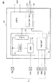
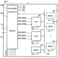
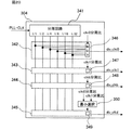
図1には、本発明にかかるデータ処理装置の一例とされるマイクロコンピュータが示される。 FIG. 1 shows a microcomputer as an example of a data processing apparatus according to the present invention.
図1に示されるマイクロコンピュータ1は、第1CPU(CPU1)10、第2CPU(CPU2)11、デバッグ回路(DEBUG)2、各種周辺モジュール(MODL)12−1〜12−nを含み、特に制限されないが、公知の半導体集積回路製造技術により、単結晶シリコン基板などの一つの半導体基板に形成される。第1CPU10、第2CPU11、及び各種周辺モジュール12−1〜12−nは、システムバス13により互いに信号のやり取りが可能に結合される。デバッグ回路2は、上記システムバス13、上記第1CPU10及び上記第2CPU11に結合され、上記第1CPU10や上記第2CPU11で実行されるユーザプログラムのデバッグを可能とする。デバッグ回路2には、システムバス13のデータ(システムバスデータ)SYSB−DATAがデバッグ回路2に伝達される。デバッグ回路2と、第1CPU10との間では、デバッグのために必要とされる各種信号、すなわち、ユーザプログラムの実行再開を許可または抑止させるためのストール制御信号STL−CNT、ブレークからの復帰命令を実行中か否かというCPUの状態を表す復帰命令実行信号RTB−CNT、ブレーク状態か否かというCPUの状態を表すブレークアクノリッジ信号BRK−ACK、ユーザプログラムの実行停止要求のためのブレークリクエスト信号BRK−REQ、CPUバスデータCPUB−DATA、及びリセット要求のためのリセット信号RSTのやり取りが可能とされる。また同様に、デバッグ回路2と、第2CPU11との間では、デバッグのために必要とされる各種信号、すなわち、ストール制御信号STL−CNT、復帰命令実行信号RTB−CNT、ブレークアクノリッジ信号BRK−ACK、ブレークリクエスト信号BRK−REQ、CPUバスデータCPUB−DATA、及びリセット信号RSTのやり取りが可能とされる。
The
デバッグ回路2によりブレークリクエスト信号BRK−REQがアサートされることにより、第1CPU10や第2CPU11に対してブレーク(ユーザプログラムの実行停止)を要求することができる。第1CPU10又は第2CPU11によりブレークアクノリッジ信号BRK−ACKがアサートされることにより、デバッグ回路2は、第1CPU10や第2CPU11のブレーク状態を把握することができる。また、デバッグ回路2は、第1CPU10又は第2CPU11により復帰命令実行信号RTB−CNTがアサートされることにより、デバック回路2は、第1CPU10や第2CPU11においてブレーク状態に遷移することによりデバッグ処理が行われ、デバッグ処理が完了後に再度ユーザプログラムの実行を開始できる、つまりユーザプログラムへの復帰直前である状態を把握することが可能となる。デバッグ回路2によりストール制御信号STL−CNTがネゲートされることにより、第1CPU10や第2CPU11に対して、ブレークされた状態からの復帰によるユーザプログラム実行開始を指示することができる。デバッグ回路2は、CPUバスデータCPUB−DATAにより、第1CPU10や第2CPU11によって図示はされないがCPUバスに出力される各種情報を把握することができる。デバッグ回路2によってリセット信号RSTがアサートされることにより、第1CPU10や第2CPU11をリセットすることができる。上記第1CPU10で実行されるユーザプログラムのデバッグ結果や、上記第2CPU11で実行されるユーザプログラムのデバッグ結果は、デバッグ回路2により共通のデバッグ端子5を介してマイクロコンピュータ1の外部に出力される。
When the break request signal BRK-REQ is asserted by the
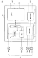
図2には、上記デバッグ回路2の構成例が示される。
FIG. 2 shows a configuration example of the
上記デバッグ回路2は、特に制限されないが、図2に示されるようにデバッグインタフェース(DEBUGI/F)21、実行制御回路(PRC−CNT)22、及びブレーク制御回路(BRK−CNT)23を含んで成る。
Although not particularly limited, the
実行制御回路22は、上記第1CPU10及び上記第2CPU11におけるユーザプログラム実行を制御する機能を有し、ブレーク状態からの復帰によるユーザプログラム実行開始タイミングが上記第1CPU10と上記第2CPU11との間で一致する同時実行モード(同時実行)と、ブレーク状態からの復帰によるユーザプログラム実行開始を上記CPU毎に個別的に制御可能な個別的実行モード(個別実行)とを含む。上記第1CPU10及び上記第2CPU11から伝達されたブレークアクノリッジ信号BRK−ACKが実行制御回路22に取り込まれる。実行制御回路22は、伝達されたブレークアクノリッジ信号BRK−ACKもしくは復帰命令実行信号RTB−CNTの何れかを参照することにより、対応するCPUの状態を検知し、それに基づいて複数のCPU分のアサートされていたストール制御信号STL−CNTを同一タイミングでネゲートする同時実行モードを有する。上記第1CPU10及び上記第2CPU11において、アサートされていたストール制御信号STL−CNTがネゲートされた場合、復帰命令RTBが実行されることによって復帰され、ユーザプログラムの実行が開始される。同時実行モードにおいては、複数のCPU分のアサートされていたストール制御信号STL−CNTが同一タイミングでネゲートされるため、上記第1CPU10と上記第2CPU11とで、ブレーク状態からの復帰によるユーザプログラムが同時実行される。ここで「同時実行」には、タイミング的に完全に一致している場合のみならず、数クロック分のずれを含むものと解されたい。同時実行モードと個別的実行モードとは、デバッグ効率を考慮して適宜に選択することができる。
The
上記ブレーク制御回路23は、CPUバスデータCPUB−DATAやブレークアクノリッジ信号BRK−ACKに基づいて上記第1CPU10及び上記第2CPU11に対するブレーク動作を制御する。このブレーク動作の制御には、上記第1CPU10及び上記第2CPU11の何れかにおいてブレーク条件が成立した場合に、それに呼応して上記第1CPU10及び上記第2CPU11に対して、ブレークリクエスト信号BRK−REQを同時にアサートする同時ブレークモードと、上記第1CPU10及び上記第2CPU11の何れかにおいてブレーク条件が成立した場合に、それに呼応して上記第1CPU10及び上記第2CPU11の何れかに対応するブレークリクエスト信号BRK−REQをアサートする個別的ブレークモードとを有する。この同時ブレークモードと個別的ブレークモードとは、デバッグ効率を考慮して適宜に選択することができる。この選択を可能にするには、ブレーク制御回路23内にブレーク条件設定レジスタを設け、このレジスタにブレークモードを設定するようにすれば良い。ここで、上記同時ブレークには、上記第1CPU10及び上記第2CPU11のブレークタイミングが完全に揃っている場合の他、数クロック分のずれがある場合をも含むものと解されたい。
The
図5には、上記実行制御回路(PRC−CNT)22の構成例が示される。 FIG. 5 shows a configuration example of the execution control circuit (PRC-CNT) 22.
上記実行制御回路(PRC−CNT)22は、特に制限されないが、ストール制御信号生成回路221、及び同時実行制御レジスタ222を含んで成る。
The execution control circuit (PRC-CNT) 22 includes a stall control
ストール制御信号生成回路221は、ブレークアクノリッジ信号BRK−ACKに対応するCPUの状態を検知し、同時実行制御レジスタ222の設定に基づいて上記第1CPU10及び上記第2CPU11における復帰命令の実行を制御する。この復帰命令の実行制御には、上記第1CPU10及び上記第2CPU11に対応するストール制御信号STL−CNTをアサートしておき、上記第1CPU10及び上記第2CPU11に対応するブレークアクノリッジ信号BRK−ACKのアサートを検知して、上記第1CPU10及び上記第2CPU11に対応するストール制御信号STL−CNTを同時にネゲートする同時実行モードと、上記第1CPU10及び上記第2CPU11に対応するストール制御信号STL−CNTをネゲートした状態のまま保持し、復帰命令に到達した上記第1CPU10及び上記第2CPU11から個別的に復帰命令を実行する個別的実行モードとを有する。この同時実行モードと個別的実行モードとは、デバッグ効率を考慮して適宜に選択することができる。この選択を可能にするには、上記ブレーク条件設定レジスタにブレークモードを設定するようにすれば任意のモードで実行することが可能となる。
The stall control
上記ストール制御信号生成回路221は、上記複数のCPUの状態を検知するための入力信号として、復帰命令の実行が完了したことを示すブレークアクノリッジ信号BRK−ACKを使用する。例えば、同時実行モードにおいて、デバッグ回路22の制御によるデバッグ処理後に、上記第1CPU10が先に復帰命令の実行に到達し、上記第2CPU11が後に復帰命令の実行に到達する場合、上記第1CPU10は対応するアサートされたストール制御信号STL−CNTを参照し復帰命令の実行をストールさせる。一方、上記第2CPU11は対応するアサートされたストール制御信号STL−CNTを参照せず復帰命令の実行を完了し、ブレークアクノリッジ信号BRK−ACKをアサートする。上記第2CPU11は対応するブレークアクノリッジ信号BRK−ACKのアサートにより、ストール制御信号生成回路221はストール制御信号STL−CNTを同時にネゲートする。上記第1CPU10は対応するストール制御信号STL−CNTを参照することによりネゲートされたことを検知し、復帰命令を実行する。ストール制御信号STL−CNTの参照は、例えば上記第1CPU10及び上記第2CPU11が同時実行制御レジスタ222を読み出す動作で実現する。また、上記第1CPU10及び上記第2CPU11は、デバッグ回路22から出力されるストール制御信号によってその状態を知ることができる。上記ストール制御信号生成回路221において、ブレークアクノリッジ信号BRK−ACKを使用して同時実行モードを実現する場合、上記第1CPU10及び上記第2CPU11における復帰命令の実行順序を事前に知る必要がある。
The stall control
上記ストール制御信号生成回路221は、上記複数のCPUの状態を検知するための入力信号として、ブレークアクノリッジ信号BRK−ACKの代わりに復帰命令実行信号RTB−CNTを使用することができる。例えば、同時実行モードにおいて、上記第1CPU10と上記第2CPU11の復帰命令を同時に実行させる場合、上記第1CPU10と上記第2CPU11に対応する復帰命令実行信号RTB−CNTが全てアサートされることにより、ストール制御信号生成回路221はストール制御信号STL−CNTを同時にネゲートする。上記第1CPU10と上記第2CPU11は、対応するストール制御信号STL−CNTを参照することによりネゲートされたことを検知し、復帰命令を実行する。上記ストール制御信号生成回路221において、復帰命令実行信号RTB−CNTを使用して同時実行モードを実現する場合、上記第1CPU10及び上記第2CPU11における復帰命令の実行順序を事前に知る必要はない。復帰命令実行信号RTB−CNTは対応するCPUにおいて復帰命令の実行中にアサートされ、復帰命令の実行完了前でブレーク状態からの復帰を検知できる。このため、復帰命令実行信号RTB−CNTを使用した同時実行は、ブレークアクノリッジ信号BRK−ACKを使用した同時実行よりもクロックのずれを少なくできる。
The stall control
同時実行制御レジスタ222は、同時実行モードと個別的実行モードの設定を可能にする。具体的には、上記第1CPU10及び上記第2CPU11とに対応するビットを複数設け、その論理値が“0”の場合には上記第1CPU10及び上記第2CPU11における復帰命令の実行は個別的実行モードに設定される。例えば上記第1CPU10に対応するビットの論理値が“0”の場合、上記第1CPU10での復帰命令と上記第2CPU11での復帰命令とは、個別的に実行される。これに対して、ビットの論理値が“1”の場合には上記第1CPU10及び上記第2CPU11における復帰命令の実行は同時実行モードに設定される。例えば上記第1CPU10に対応するビットの論理値が“1”の場合、上記第2CPU11での復帰命令の実行は上記第1CPU10での復帰命令と同時に実行するよう制御される。
The concurrent
上記同時実行制御レジスタ222は、1ビットの構成であってもよい。具体的には、同時実行制御レジスタが論理値“0”の場合には個別的実行モードが指定される。この場合、上記第1CPU10及び上記第2CPU11での復帰命令の実行は、対応するブレークアクノリッジ信号BRK−ACKもしくは復帰命令実行信号RTB−CNTに応じて、個別的に実行される。これに対して、同時実行制御レジスタが論理値“1”の場合には同時実行モードが指定される。上記第1CPU10及び上記第2CPU11に対して、アサートされたストール制御信号STL−CNTを同時にネゲートすることにより、復帰命令が上記第1CPU10と上記第2CPU11とで同時に実行される。
The simultaneous
図6には、上記ブレーク制御回路23の構成例が示される。
FIG. 6 shows a configuration example of the
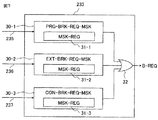
上記ブレーク制御回路23は、特に制限されないが、図6に示されるようにプログラム要因ブレーク要求回路(PRG−BRK−REQ)230、外部要因ブレーク要求回路(EXT−BRK−REQ)231、条件成立ブレーク要求回路(CON−BRK−REQ)232、ブレーク要求マスク回路233,234を含んで成る。
The
プログラム要因ブレーク要求回路230は、例えばユーザプログラムの実行において、所定のブレーク命令が実行された場合に、ブレークアクノリッジ信号BRK−ACKを第1CPU10又は第2CPU11より取り込み、それに基づいてブレーク要求信号235をアサートする。つまり、ブレークアクノリッジ信号BRK−ACKによってCPUのブレーク状態を把握し、それに従って他のCPUをブレークさせるためのブレーク要求信号235をアサートする。このブレーク要求信号235は、後段のブレーク要求マスク回路233,234に伝達される。
The program factor
上記外部要因ブレーク要求回路231は、図示しない外部端子を介してこのマイクロコンピュータ1の外部から与えられたブレーク要因に基づいてブレーク要求信号236をアサートする。このブレーク要求信号236は、後段のブレーク要求マスク回路233,234に伝達される。条件成立ブレーク要求回路(CON−BRK−REQ)232は、各CPUのCPUバスデータCPUB−DATAおよびシステムバスデータSYSB−DATAをモニタして、このCPUバスデータCPUB−DATAが、予め設定されたブレーク条件と一致した場合にブレーク要求信号237をアサートする。このブレーク要求信号237は、後段のブレーク要求マスク回路233,234に伝達される。
The external factor
ブレーク要求マスク回路233,234は、上記CPU10,11に対応して配置され、設定されたブレークモードに応じて上記ブレーク要求信号235,236,237をマスクすることによって、ブレーク対象とされるCPUに対してのみ、ブレークリクエスト信号BRK−REQをアサートする。
The break
ブレーク要求マスク回路233は、第1CPU10に対するブレークリクエスト信号BRK−REQをアサートし、ブレーク要求マスク回路234は、第2CPU11対するブレークリクエスト信号BRK−REQをアサートする。ブレーク要求マスク回路233,234は、互いに同一構成とされる。例えばブレーク要求マスク回路233は、図7に示されるように、プログラム要因ブレーク要求マスク部(PRG−BRK−REQ−MSK)30−1、外部要因ブレーク要求マスク部(EXT−BRK−REQ−MSK)30−2、条件成立ブレーク要求マスク部(CON−BRK−REQ)30−3、及びそれら出力のオア論理を得るオアゲート32を含んで成る。プログラム要因ブレーク要求マスク部30−1、外部要因ブレーク要求マスク部30−2、及び条件成立ブレーク要求マスク部30−3は、それぞれ図6に示されるブレーク要求マスク回路233、234に対応しており、伝達されたブレーク要求信号235、236、237のマスク処理を行う。すなわち、プログラム要因ブレーク要求マスク部30−1は、マスクレジスタ(MSK−PRG)31−1を含み、このマスクレジスタ31−1の設定情報に従ってブレーク要求信号235のマスク処理を行う。外部要因ブレーク要求マスク部30−2は、マスクレジスタ(MSK−PRG)31−2を含み、このマスクレジスタ31−2の設定情報に従ってブレーク要求信号236のマスク処理を行う。条件成立ブレーク要求マスク部30−2は、マスクレジスタ(MSK−PRG)31−3を含み、このマスクレジスタ31−3の設定情報に従ってブレーク要求信号237のマスク処理を行う。例えば、マスクレジスタ31−1,31−2,31−3に論理値“1”が設定されている場合には、対応するブレーク要求信号235、236、237がマスクされずにそのまま出力され、オアゲート32でオア論理が得られる。それに対してマスクレジスタ31−1,31−2,31−3に論理値“0”が設定されている場合には、対応するブレーク要求信号235、236、237がマスクされる。マスクされた場合、それに対応する出力信号は、論理値“0”に固定される。このようなマスク処理により、ブレーク要因が第1CPU10及び第2CPU11の何れにあるかにかかわらず、任意のCPU10,11に対してブレークリクエスト信号BRK−REQをアサートすることができる。例えば、ブレーク要求マスク回路233でブレーク要求信号235,236,237がマスクされる場合には、第1CPU10に対するブレークリクエスト信号BRK−REQはアサートされなくなる。また、ブレーク要求マスク回路234でブレーク要求信号235,236,237がマスクされる場合には、第2CPU11に対するブレークリクエスト信号BRK−REQはアサートされなくなる。一方、ブレーク要求マスク回路233,234の何れにおいてもブレーク要求信号235,236,237がマスクされない場合には、ブレーク要因が第1CPU10及び第2CPU11の何れにあるかにかかわらず、第1CPU10及び第2CPU11の双方に対してブレークリクエスト信号BRK−REQがアサートされることにより、同時ブレークが可能とされる。
The break
図8には、図6における条件成立ブレーク要求回路(CON−BRK−REQ)232の構成例が示される。 FIG. 8 shows a configuration example of the condition satisfaction break request circuit (CON-BRK-REQ) 232 in FIG.
条件成立ブレーク要求回路232は、特に制限されないが、図8に示されるように複数の条件一致判定回路(CND−JUD)25−1,25−2,…,25−n(nは自然数)と、シーケンシャルブレーク判定回路27とを含んで成る。複数の条件一致判定回路25−1,25−2,…,25−nは、それぞれブレーク条件レジスタ(BRK−CND−REG)26−2,26−2,…,26−nを含み、第1CPU10及び第2CPU11からのCPUバスデータCPUB−DATAが上記ブレーク条件レジスタ26−2,26−2,…,26−nの設定情報に一致した場合に、対応する条件一致フラグCNDM−FLGをアサートする機能を有する。上記ブレーク条件レジスタ26−1,26−2,…,26−nは、例えば図9に示されるように、CPU選択フィールド310と、バス状態選択フィールド320とを含む。上記CPU選択フィールド310には、ブレーク条件一致判定の対象となる2ビットのCPU識別情報が設定される。このCPU識別情報は、例えばブレーク条件一致判定の対象が第1CPU10のみの場合は“01”とされ、ブレーク条件一致判定の対象が第2CPU11のみの場合は“10”とされ、ブレーク条件一致判定の対象が第1CPU10及び第2CPU11の双方の場合は“11”とされる。上記バス状態選択フィールド320には、コンペア条件(ブレーク条件)が設定される。コンペア条件としては、特に制限されないが、バス指定、アドレス、コマンド、データ、バスサイクルなどが含まれる。また、上記ブレーク条件レジスタを複数有することにより、複数のコンペア条件(ブレーク条件)を設定することが可能となり、一つのシステムデバッグ設定によって多数のコンペア条件を設定でき、デバッグ効率を向上することが可能となる。
Although the condition satisfaction
シーケンシャルブレーク判定回路27は、上記複数の条件一致判定回路25−1,26−2,…,25−nからの条件一致フラグCNDM−FLGを取り込んで、シーケンシャルブレーク条件が成立したか否かを判定し、当該ブレーク条件が成立した場合にシーケンシャルブレーク条件一致フラグSCNDM−FLGをアサートする。シーケンシャルブレーク条件は、複数ブレーク条件の組み合わせとされ、各ブレーク条件の一致が一定の順序に従って成立した場合に一致したとみなされる。シーケンシャルブレーク条件は、シーケンシャルブレーク判定回路27内のシーケンシャルブレーク条件レジスタ28に設定され、シーケンシャルブレーク判定回路27は、このシーケンシャルブレーク条件レジスタ28に設定情報に基づいて、シーケンシャルに起こり得るブレーク条件が成立したか否かを判定する。例えば、条件一致判定回路25−2でブレーク条件が成立した後に、条件一致判定回路25−1でブレーク条件が成立した場合が、シーケンシャルブレーク条件として、シーケンシャルブレーク条件レジスタ28に設定されたとき、当該条件が成立した場合にシーケンシャルブレーク条件一致フラグSCNDM−FLGがアサートされる。このようなシーケンシャルブレークにより、条件一致判定回路25−1〜25−nでのブレーク条件判定に加えて、より高度なブレーク条件判定が可能とされる。
The sequential
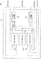
図3には、上記デバッグインタフェース回路21の構成例が示される。
FIG. 3 shows a configuration example of the
上記デバッグインタフェース回路21は、特に制限されないが、図3に示されるようにJTAG(Joint Test Action Group)制御部(JTAG−CNT)211、及び制御回路(CNTR)212を含んで成る。
Although not particularly limited, the
上記JTAG制御部211は、バイパスレジスタ(SDBPR)51、シフトレジスタ(S−REG)53、マルチプレクサ(MUX)52、及びTAP(Test Access Port)制御回路(TAP−CNT)54を含んで成り、上記共通の複数のデバッグテスト端子5を介して、このマイクロコンピュータ1の外部との間で、JTAG所定の信号であるテスト入力データ信号TDI、テスト出力データ信号TDO、クロック信号TCK、テスト制御信号TMS、リセット信号/TRSTのやり取りが可能とされる。TAP制御回路(TAP−CNT)54の制御により、IEEE準拠の内部制御スキャン方式(JTAGスキャン方式)を用いて、TDIより入力される値を制御のためのコマンド又はデータと解釈し、デバッグ情報の外部出力が可能とされる。
The
上記制御回路212は、上記JTAG制御部211内のシフトレジスタ53に結合されることで、上記JTAG制御部211との間でデータのやり取りが可能とされ、実行制御回路22やブレーク制御回路23との間で、制御信号やデータなどの各種信号CNTのやり取りが可能とされる。上記制御回路212は、リセット制御のためのリセット制御レジスタ(RST−CNT−REG)55を含む。
The
上記制御回路212は、上記リセット制御レジスタ55の設定情報に従って、上記第1CPU10及び第2CPU11をリセットするためのリセット信号RSTを形成する。上記リセットレジスタ55は、上記第1CPU10及び第2CPU11に1対1で対応するビットを含む。この制御回路212は、上記第1CPU10及び第2CPU11に対応するビットに論理値“1”を設定することにより上記第1CPU10及び第2CPU11に対するリセット信号RSTをアサートし、上記第1CPU10及び第2CPU11に対応するビットに論理値“0”を設定することにより上記第1CPU10及び第2CPU11に対するリセット信号RSTをネゲートする個別的リセットモードを有する。また、この制御回路212は、上記第1CPU10と第2CPU11とに対応するリセット信号RSTを同時にアサートしその後ネゲートする同時リセットモードを有する。この個別的リセットモードと同時リセットモードとは、デバッグ効率を考慮して適宜に選択することができる。
The
図4には、上記デバッグインタフェース回路21の別の構成例が示される。
FIG. 4 shows another configuration example of the
図4に示される構成が図3に示されるのと大きく相違するのは、リセット制御回路(RST−CNT)213が設けられ、それに伴い、制御回路212内のリセット制御レジスタ55が省略されている点である。
The configuration shown in FIG. 4 is greatly different from that shown in FIG. 3 in that a reset control circuit (RST-CNT) 213 is provided, and accordingly, the
上記制御回路212は、上記JTAG制御部211内のシフトレジスタ53に結合されることで、上記JTAG制御部211との間でデータのやり取りが可能とされ、実行制御回路22やブレーク制御回路23との間で、制御信号やデータなどの各種信号CNTのやり取りが可能とされる。リセット制御回路(RST−CNT)213は、上記JTAG制御部211内のシフトレジスタ53とTAP制御回路(TAP−CNT)54とに結合されることで、TDIより入力されるリセット用のコマンドを解釈し、上記第1CPU10及び上記第2CPU11をリセットするためのリセット信号RSTを個別的にアサート又はネゲートする個別的リセットモードを有する。また、このリセット制御回路213は、上記第1CPU10と第2CPU11とに対応するリセット信号RSTを同時にアサートし、その後ネゲートする同時リセットモードを有する。この個別的リセットモードと同時リセットモードとは、デバッグ効率を考慮して適宜に選択することができる。
The
上記の例によれば、以下の作用効果を得ることができる。 According to the above example, the following effects can be obtained.
(1)第1CPU10、第2CPU11の何れかにおいてブレーク条件が成立した場合に、それに呼応して上記CPU10,11を同時ブレーク可能な同時ブレークモードを有することから、上記第1CPU10、第2CPU11の何れかにおいてブレーク条件が成立した後における上記複数のCPU10,11間での命令実行のずれを最小限に抑えることができる。また、ブレーク状態からの復帰によるユーザプログラム実行開始タイミングが上記第1CPU10、第2CPU11間で一致可能な同時実行モードを有することから、ブレークされた状態からの復帰によるユーザプログラム実行のタイミング的なずれを上記CPU10,11間で最小限に抑えることができる。これにより、第1CPU10、第2CPU11を含むマイクロコンピュータ1のシステムデバッグにおけるデバッグ効率向上を達成することができる。
(1) Since either of the
(2)ブレーク要求マスク回路233,234は、上記CPU10,11に対応して配置され、設定されたブレークモードに応じて上記ブレーク要求信号235,236,237をマスクすることによって、ブレーク対象とされるCPUに対してのみ、ブレークリクエスト信号BRK−REQがアサートされる。このようなマスク処理により、ブレーク要因が第1CPU10及び第2CPU11の何れにあるかにかかわらず、任意のCPU10,11に対してブレークリクエスト信号BRK−REQをアサートすることができる。
(2) The break
(3)シーケンシャルブレーク判定回路27は、上記複数の条件一致判定回路25−1,25−2,…,25−nからの条件一致フラグCNDM−FLGを取り込んで、シーケンシャルブレーク条件が成立したか否かを判定し、当該ブレーク条件が成立した場合にシーケンシャルブレーク条件一致フラグSCNDM−FLGをアサートする。このようなシーケンシャルブレークが行われる場合には、条件一致判定回路25−1〜25−nでのブレーク条件判定に加えて、より高度なブレーク条件判定が可能とされる。
(3) The sequential
(4)デバッグインタフェース21に含まれるリセット制御回路213は、個別的にリセット信号RSTをアサート又はネゲートする個別的リセットモードを有する。このような個別的リセットを適用すれば、あるユーザプログラムを実行している一方のCPUを動作させたまま、別のユーザプログラムを実行している他方のCPUをリセットすることが可能であるため、より詳細なCPUの制御が可能となり、デバッグ効率の向上を達成することができる。
(4) The
図10には、本発明にかかるデータ処理装置の一例とされるマイクロコンピュータの別の構成例が示される。 FIG. 10 shows another configuration example of a microcomputer as an example of the data processing apparatus according to the present invention.
図10に示されるマイクロコンピュータ1は、第1CPU100、第2CPU110、デバッグ回路(DEBUG)200、各種周辺モジュール(MODL)120−1〜120−n、DMAC(ダイレクト・メモリ・アクセス・コントローラ)140、及びクロックモジュール(CLK−MODL)300を含み、特に制限されないが、公知の半導体集積回路製造技術により、単結晶シリコン基板などの一つの半導体基板に形成される。第1CPU100、第2CPU110、DMAC140、デバッグ回路200、及び各種周辺モジュール120−1〜120−nは、システムバス130を介して結合される。上記第1CPU100、上記第2CPU110、及びDMAC140は、それぞれシステムバス130についてのバスマスタとされ、システムバス130のバス権を取得して各種データの転送制御を行うことができる。
The
デバッグ回路200は、上記システムバス130、上記第1CPU100及び上記第2CPU110に結合され、上記第1CPU100や上記第2CPU110で実行されるユーザプログラムのデバッグを可能とする。CPU100からデバッグ回路200に、分岐情報BRA−INF#0や、CPUバス情報BUS−INF#0が伝達される。デバッグ回路200とCPU100との間でデバッグアクセス情報ACC−INF#0のやり取りが可能とされる。CPU110からデバッグ回路200に、分岐情報BRA−INF#1や、CPUバス情報BUS−INF#1が伝達される。デバッグ回路200とCPU100との間でデバッグアクセス情報ACC−INF#1のやり取りが可能とされる。
The
クロックモジュールCLK−MODL300は、互いに周波数が異なる複数のクロック信号を形成する。複数のクロック信号には、デバッグ用クロック信号clkd、CPU用クロック信号clki0,clki1、及び周辺モジュール用クロック信号clkbが含まれる。デバッグ用クロック信号clkdは、デバッグ回路200に供給される。CPU用クロック信号clki0は、CPU100及びデバッグ回路200に供給される。CPU用クロック信号clki1は、CPU110及びデバッグ回路200に供給される。周辺モジュール用クロック信号clkbは、周辺モジュール120−1〜120−n、DMAC140、CPU100,110、及びデバッグ回路200に供給される。
The clock module CLK-
上記第1CPU100で実行されるユーザプログラムのデバッグ結果や、上記第2CPU110で実行されるユーザプログラムのデバッグ結果は、デバッグ回路200から共通のデバッグ端子50を介してマイクロコンピュータ1の外部に出力することができる。また上記デバッグ結果のうちトレース情報については専用のトレース端子群60を介して外部出力可能とされる。
The debug result of the user program executed by the
図11には、上記第1CPU100の構成例が示される。
FIG. 11 shows a configuration example of the
上記第1CPU100は、特に制限されないが、CPUコア101、モジュール内メモリ102、及びバスブリッジ103を含み、それらがCPUバス104によって相互に信号のやり取り可能に結合されて成る。CPUバス104からCPUバス情報BUS−INF#0が取り出される。第1CPU100は、演算処理のための所定のプログラムを実行する。モジュール内メモリ102には、上記CPUコア101で実行されるプログラムが格納されたROM(リード・オンリー・メモリ)や、上記CPUコア101での演算処理における作業領域などとして使用されるRAM(ランダム・アクセス・メモリ)が含まれる。プログラム実行における分岐情報BRA−INF#0はCPUコア101から取り出される。CPUバス104とシステムバス130とはバスブリッジ103によって結合される。このバスブリッジ103からデバッグアクセス情報ACC−INF#0が取り出される。
The
尚、第2CPU110も、上記第1CPU100と同様に構成される。
The
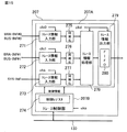
図12には上記デバッグ回路200の構成例が示される。
FIG. 12 shows a configuration example of the
上記デバッグ回路200は、特に制限されないが、デバッグインタフェース201、実行制御回路202、ブレーク制御回路203、デバッグアクセス回路204、第1トレース取得回路205、及び第2トレース取得回路207を含んで成る。
Although not particularly limited, the
実行制御回路202は、デバッグの実行を制御する。ブレーク制御回路203は、予め設定されたブレーク条件に基づくブレーク動作の制御を行う。デバッグアクセス回路204は、上記システムバス130を介してデバッグアクセスを行う。上記バスブリッジ103にはデバッグアクセス情報ACC−INF#0用の信号線も接続される。これによって、デバッグ回路DEBUG200は、システムバス上のデバイスをアクセスすることができる。
The
上記デバッグインタフェース201は、デバッグ端子50、上記実行制御回路202、ブレーク制御回路203、及びデバッグアクセス回路204に結合され、外部との間でJTAG(Joint Test Action Group)仕様による所定信号のやり取りを可能とする。
The
上記第1トレース取得回路205及び上記第2トレース取得回路207は、システム内のバスの状態を監視し、所定の条件に一致した状態を取得する機能を有する。上記第1トレース取得回路205及び上記第2トレース取得回路207には、分岐情報BRA−INF#0,BRA−INF#1、CPUバス情報BUS−INF#0,BUS−INF#1等のトレース情報が取り込まれる。上記第1トレース取得回路205及び上記第2トレース取得回路207は、それぞれシステムバス130に結合され、このシステムバス130を介してトレースに関する各種制御情報などのやり取りが可能とされる。上記第1トレース取得回路205で取得されたトレース情報は、必要に応じてシステムバス130に出力することができる。第2トレース取得回路207は、トレース端子60に結合されており、このトレース端子60を介して、上記第2トレース取得回路207で取得されたトレース情報の外部出力が可能とされる。
The first
図13には上記第1トレース取得回路205の構成例が示される。
FIG. 13 shows a configuration example of the first
上記第1トレース取得回路205は、トレース処理を行うトレース処理部205Aと、このトレース処理部205Aでのトレース処理を制御するトレース制御部205Bとを含む。上記トレース処理部205Aは、トレース情報入力部251〜253、同期化部255〜257、トレース情報処理部258、選択部259,260、同期化部261、及びトレースメモリ262を含む。
The first
上記トレース情報入力部251は、CPU用クロック信号clki0に同期して分岐情報BRA−INF#0及びCPUバス情報BUS−INF#0を取り込む。取り込まれた情報は、後段の同期化部255に伝達され、ここでデバッグ用クロック信号clkdに同期化されてから後段のトレース情報処理部258に伝達される。
The trace
上記トレース情報入力部252は、CPU用クロック信号clki1に同期して分岐情報BRA−INF#1及びCPUバス情報BUS−INF#1を取り込む。取り込まれた情報は、後段の同期化部256に伝達され、ここでデバッグ用クロック信号clkdに同期化されてから後段のトレース情報処理部258に伝達される。
The trace
上記トレース情報入力部253は、周辺モジュール用クロック信号clkbに同期してシステムバス130におけるシステムバス情報SYS−INFを取り込む。取り込まれた情報は、後段の同期化部257に伝達され、ここでデバッグ用クロック信号clkdに同期化されてから後段のトレース情報処理部258に伝達される。
The trace
上記トレース情報処理部258は、上記同期化部255,256,257を介して伝達された情報を、トレース制御部205Bに予め設定された条件に従って選択的に取り込むための機能を有する。上記トレース情報処理部258の動作はデバッグ用クロック信号clkdに同期動作される。上記トレース情報処理部258によって選択的に取り込まれた情報は、選択部259,260に伝達される。
The trace
上記トレースメモリ262は、デバッグ用クロック信号clkdに同期動作され、上記選択部259を介して伝達された情報を格納するための第1格納領域263と、上記選択部260を介して伝達された情報を格納するための第2格納領域264とを有する。上記第1格納領域263に格納された情報は、選択部259、同期化部260、及びトレース制御部205Bを介してシステムバス130に伝達することができる。また、上記第2格納領域264に格納された情報は、選択部260、同期化部261、及びトレース制御部205Bを介してシステムバス130に伝達することができる。同期化部261は、トレース制御部205Bから伝達された情報をデバッグ用クロック信号clkdに同期化する機能と、選択部259,260を介して伝達された情報を周辺モジュール用クロック信号clkbに同期化する機能を有する。
The
上記トレース制御部205Bは、制御レジスタ254を含み、この制御レジスタ254に設定された情報に従って、上記トレース処理部205Aの動作が制御される。上記トレース制御部205Bは、周辺モジュール用クロック信号clkbに同期動作される。
The
図14には、上記トレースメモリ262に格納されるトレース情報のデータのフォーマットが示される。
FIG. 14 shows the format of the trace information data stored in the
分岐情報パケットBRA−PKTは、分岐種別フィールド、タイムスタンプフィールド、分岐先アドレスフィールド、及び分岐元データフィールドを含む。CPUバス情報パケットBUS−PKTは、CPUバスコマンドフィールド、タイムスタンプフィールド、CPUバスアドレスフィールド、及びCPUバスデータフィールドを含む。システムバス情報パケットSYS−PKTは、システムバスコマンドフィールド、タイムスタンプフィールド、システムバスアドレスフィールド、システムバスデータフィールドを含む。上記タイムスタンプは、パケットが生成された時刻を示すものであり、図示しないカウンタのカウント値が格納される。デバッグ回路200へ供給される分岐情報BRA−INF#0、BRA−INF#1より与えられた情報に基づき、分岐種別、分岐先アドレス、分岐元アドレスを含む上記分岐情報パケットBRA−PKTが構成される。CPUバス情報BUS−INF#0、BUS−INF#1より与えらた情報に基づき、CPUバスコマンド、CPUバスアドレス、CPUバスデータを含むCPUバス情報パケットBUS−PKTが構成される。システムバス情報SYS−INFより与えられた情報に基づき、システムバスコマンド、システムバスアドレス、システムバスデータを含む上記システムバス情報パケットSYS−PKTが構成される。
The branch information packet BRA-PKT includes a branch type field, a time stamp field, a branch destination address field, and a branch source data field. The CPU bus information packet BUS-PKT includes a CPU bus command field, a time stamp field, a CPU bus address field, and a CPU bus data field. The system bus information packet SYS-PKT includes a system bus command field, a time stamp field, a system bus address field, and a system bus data field. The time stamp indicates the time when the packet is generated, and stores the count value of a counter (not shown). Based on the information given from the branch information BRA-
図15には、上記第2トレース取得回路207の構成例が示される。
FIG. 15 shows a configuration example of the second
上記第2トレース取得回路207は、トレース処理を行うトレース処理部207Aと、このトレース処理部207Aでのトレース処理を制御するトレース制御部207Bとを含む。上記トレース処理部207Aは、トレース情報入力部271〜273、同期化部275〜277、トレース情報処理部258、及びトレース情報出力部279を含む。
The second
上記トレース情報入力部271は、CPU用クロック信号clki0に同期して分岐情報BRA−INF#0及びCPUバス情報BUS−INF#0を取り込む。取り込まれた情報は、後段の同期化部275に伝達され、ここでデバッグ用クロック信号clkdに同期化されてから後段のトレース情報処理部278に伝達される。
The trace
上記トレース情報入力部272は、CPU用クロック信号clki1に同期して分岐情報BRA−INF#1及びCPUバス情報BUS−INF#1を取り込む。取り込まれた情報は、後段の同期化部276に伝達され、ここでデバッグ用クロック信号clkdに同期化されてから後段のトレース情報処理部278に伝達される。
The trace
上記トレース情報入力部273は、周辺モジュール用クロック信号clkbに同期してシステムバス130におけるシステムバス情報SYS−INFを取り込む。取り込まれた情報は、後段の同期化部277に伝達され、ここでデバッグ用クロック信号clkdに同期化されてから後段のトレース情報処理部278に伝達される。
The trace
上記トレース情報処理部278は、上記同期化部275,276,277を介して伝達された情報を、トレース制御部207Bに予め設定された条件に従って選択的に取り込むための機能を有する。上記トレース情報処理部278の動作はデバッグ用クロック信号clkdに同期動作される。上記トレース情報処理部278によって選択的に取り込まれた情報は、トレース情報出力部280を介して外部出力可能とされる。このトレース情報出力部280は、FIFO(先入れ先出し)バッファ280を含み、このFIFOバッファ280に書き込まれた順に外部出力可能とされる。
The trace
上記トレース制御部207Bは、制御レジスタ274を含み、この制御レジスタ274に設定された情報に従って、上記トレース処理部207Aの動作が制御される。上記トレース制御部207Bは、周辺モジュール用クロック信号clkbに同期動作される。
The
図16には、上記トレース情報出力部279を介してマイクロコンピュータ1の外部へ出力されるトレース情報パケットのフォーマットが示される。
FIG. 16 shows a format of a trace information packet output to the outside of the
上記トレース情報出力部279を介して外部出力されるトレース情報パケットPKTのフォーマットは、図16に示されるように、コマンドフィールドCMD1,CMD2、及びデータフィールドDA0〜DA15を含む。コマンドフィールドCMD2は、コマンドフィールドCMD1で示されるコマンドの種類によってその有無が決定される。データフィールドDA0〜DA15は、コマンドフィールドCMD2の種類によってその有無が決定される。
The format of the trace information packet PKT output to the outside via the trace
例えばトレース情報パケットPKTの出力において、何も出力すべき情報がない場合は、CMD1にSTDBYコマンド(0000)を出力する。STDBYコマンドはCMD1だけで完了する。 For example, when there is no information to be output in the output of the trace information packet PKT, the STDBY command (0000) is output to CMD1. The STDBY command is completed only by CMD1.
例えば分岐トレース情報をトレース情報パケットPKTのフォーマットに従って出力する場合は、コマンドフィールドCMD1にBGCコマンド(0100)を出力する。BGCコマンドの場合、引き続いてコマンドフィールドCMD2を出力する。CMD2コマンドでは、その後に出力するデータフィールドの個数を示す。データフィールドDA0〜DA15には分岐元のアドレスと分岐先のアドレスが格納される。このデータフィールドは必要に応じて圧縮されている。このため、データフィールドの個数は一定ではない。圧縮方法の詳細は特に説明はしないが、例えば、分岐先アドレスを分岐元アドレスとの差分で表現する、などの方法がとられる。 For example, when branch trace information is output according to the format of the trace information packet PKT, a BGC command (0100) is output to the command field CMD1. In the case of the BGC command, the command field CMD2 is output subsequently. The CMD2 command indicates the number of data fields to be output thereafter. In the data fields DA0 to DA15, a branch source address and a branch destination address are stored. This data field is compressed as necessary. For this reason, the number of data fields is not constant. Although details of the compression method are not particularly described, for example, a method of expressing the branch destination address by a difference from the branch source address is used.
ここで、トレース情報出力部279から出力されるトレース情報パケットPKTが、第1CPU100でのプログラム実行に係るものであるのか、第2CPU110でのプログラム実行に係るものであるのかの識別を可能にするため、MSIDコマンド(0010)が設けられている。MSIDコマンドは、トレース情報出力部279から次に出力されるCPUパケットのソースデータが第1CPU100に係るものであるのか、第2CPU110に係るものであるのかを示している。コマンドフィールドCMD1として出力されるMSIDコマンドの後にはコマンドフィールドCMD2が出力される。このCMD2は「CPUID」、すなわちデータの由来を示す。例えばCMD2が、「H’0」の場合には、第1CPU100とされ、CMD2が、「H’1」の場合には、第2CPU110とされる。従って、上記トレース情報出力部279から出力されたトレース情報の受信側においては、上記「MSID」により、トレース情報出力部279から次に出力されるCPUパケットのソースデータが第1CPU100に係るものであるのか、第2CPU110に係るものであるかの識別が可能とされる。
Here, in order to make it possible to identify whether the trace information packet PKT output from the trace
図17には、上記「MSID」パケットの出力条件が示される。 FIG. 17 shows the output conditions of the “MSID” packet.
上記トレース情報出力部279から上記「MSID」パケットが出力されるには、複数のCPUをトレース対象としていること(条件A)が必要とされる。本例では、第1CPU100及び第2CPU110の双方がトレース対象としてトレース制御部207Bにおける制御レジスタ274に設定されていることが必要とされる。
In order to output the “MSID” packet from the trace
また、上記トレース情報出力部279から次にCPUパケットを出力する予定であること(条件B)が必要とされる。 Further, it is necessary to output the CPU packet next from the trace information output unit 279 (condition B).
そして、上記トレース情報出力部279から次に出力予定のCPUパケットが、N×256個(Nはゼロ以上の整数)のデータパケット(制御パケットは含まない)を出力後、最初に出力するCPUパケットであること、又は次に出力予定のCPUパケットのデータソースが、最後に出力したCPUパケットのデータソースと異なることである。
Then, the CPU packet to be output next from the trace
以上の条件が満たされたとき、トレース情報出力部279から「MSID」パケットが出力される。
When the above conditions are satisfied, an “MSID” packet is output from the trace
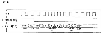
図18には、上記トレース情報出力部279からのトレース情報パケットPKTが出力される場合のタイミングが示される。
FIG. 18 shows the timing when the trace information packet PKT from the trace
トレース制御部207Bによってトレース同期信号がローレベルとされた期間において、デバッグ用クロック信号clkdに同期してトレース情報パケットPKTが出力される。これは、コマンドフィールドCMD1にBGCコマンドを出力した後で、コマンドフィールドCMD2とデータフィールドDA0〜DA5を出力した例である。最初の4個のデータフィールドには16ビットの分岐先アドレス(DA3-0、DA7-4、DA11-8およびDA15-12)が格納され、次の2個のデータフィールドには8ビットの分岐元アドレス(SA3-0、SA7-4)が格納されている。
The trace information packet PKT is output in synchronization with the debug clock signal clkd during the period when the trace synchronization signal is set to the low level by the
図19には、上記クロックモジュール300の構成例が示される。
FIG. 19 shows a configuration example of the
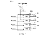
上記クロックモジュール300は、特に制限されないが、クロック制御部301,高速クロック生成器303、クロック分周器304、クロックドライバ305を含んで成る。
Although not particularly limited, the
上記高速クロック生成器303は、外部から与えられた基準クロック信号306に同期して、上記基準クロック信号306よりも周波数が高い高速クロック信号(内部クロック信号)PLL−CLKを生成する。この高速クロック生成器303は、例えばPLL(フェーズ・ロックド・ループ)によって形成される。上記上記高速クロック生成器303によって形成された高速クロック信号PLL−CLKは、後段のクロック分周器304で分周されることによって、互いに分周比が異なる複数の分周クロック信号div_clkd、div_clki0、div_clki1、div_clkbが形成される。この分周クロック信号は、例えば複数のうち一部は分周比が同じであってもよい。この複数の分周クロック信号は後段のクロックドライバ305に伝達される。クロックドライバ305は、入力された分周クロック信号div_clkd、div_clki0、div_clki1、div_clkbに基づいて負荷を駆動する。このクロックドライバ305からの出力クロック信号が、デバッグ用クロック信号clkd、CPU用クロック信号clki0,clki1、及び周辺モジュール用クロック信号clkbとされる。
The high-
上記クロック制御部301は、クロック制御レジスタ302を含み、このクロック制御レジスタ302に設定された情報に従って上記高速クロック生成器304、クロック分周器304、及びクロックドライバ305の動作を制御する。上記クロック制御レジスタ302は、システムバス130を介して第1CPU100又は第2CPU110によって書き換え可能とされる。
The
図20には、上記クロック分周器304の構成例が示される。
FIG. 20 shows a configuration example of the
上記クロック分周器304は、特に制限されないが、高速クロック生成器303から出力されたクロック信号PLL−CLKを分周するための分周回路341、選択回路342〜345、最小選択回路350を含む。
The
上記分周器341の分周出力には、クロック信号PLL−CLKの1/1分周出力、1/2分周出力、1/4分周出力、1/8分周出力、1/16分周出力、1/32分周出力が含まれる。1/1分周出力はクロック信号PLL−CLKの周波数に等しく、1/2分周出力、1/4分周出力、1/8分周出力、1/16分周出力の順に周波数が低くなる。
The divided output of the
上記選択回路342〜345は、それぞれマルチプレクサ(MUX)346〜349を含む。上記選択回路342に内蔵されるマルチプレクサ346は、CPU用クロック信号clki0に対応するclki0分周比情報に従って上記分周回路341の出力信号を選択することによってCPU用クロック信号clki0を出力する。上記選択回路343に内蔵されるマルチプレクサ347は、CPU用クロック信号clki1に対応するclki1分周比情報に従って上記分周回路341の出力信号を選択することによってCPU用クロック信号clki1を出力する。上記選択回路344に内蔵されるマルチプレクサ348は、周辺モジュール用クロック信号clkbに対応するclkb分周比情報に従って上記分周回路341の出力信号を選択することによって周辺モジュール用クロック信号clkbを出力する。周辺モジュール用クロック信号clkbは、CPU用クロック信号clki0,clki1の何れかの周波数と同じか、もしくはその何れかよりも周波数が低い。
The
上記最小選択回路350は、clki0分周比情報とclki1分周比情報とを比較して小さいほうの分周比情報を選択してマルチプレクサ349に供給する。これにより、マルチプレクサ349は、clki0分周比情報及びclki1分周比情報のうち小さいほうの分周比情報に従って上記分周回路341の出力信号を選択することによってデバッグ用クロック信号clkdを出力する。これにより、デバッグ用クロック信号clkdは、CPU用クロック信号clki0,clki1のうち、周波数の高い方のクロック信号の周波数に常に等しくされ、そのようなデバッグ用クロック信号clkdに基づいてデバッグが行われる。
The
図22には、クロック分周器304における主要部のクロック波形が示される。
FIG. 22 shows a clock waveform of a main part in the
本例においては、デバッグ用クロック信号clkdは、CPU用クロック信号clki1の周波数に等しくされている。 In this example, the debug clock signal clkd is equal to the frequency of the CPU clock signal clki1.
図23には、CPU用クロック信号の周波数が変更される場合が示される。 FIG. 23 shows a case where the frequency of the CPU clock signal is changed.
本例では、CPU用クロック信号clki0の周波数が時刻T1において変更される。誤動作防止のため、クロック周波数の変更は、最も周波数が低いクロック信号(本例の場合、clkb)の立ち上がりに同期して行われる。時刻T0から時刻T1までの間は、CPU用クロック信号clki0よりもCPU用クロック信号clki1の周波数が高いため、デバッグ用クロック信号clkdの周波数は、CPU用クロック信号clki1に等しくされている。しかし、時刻T1以降は、CPU用クロック信号clki1よりもCPU用クロック信号clki0の周波数が高いため、デバッグ用クロック信号clkdの周波数は、CPU用クロック信号clki0に等しくされている。周波数変更がある場合においても、上記最小選択回路350の制御及びその他の回路の制御によって、動的により高い周波数のCPUクロック信号がデバッグ用クロック信号clkdとして供給され、それに基づいてデバッグ回路は動作される。
In this example, the frequency of the CPU clock signal clki0 is changed at time T1. In order to prevent malfunction, the clock frequency is changed in synchronization with the rising edge of the clock signal having the lowest frequency (in this example, clkb). Since the frequency of the CPU clock signal clki1 is higher than that of the CPU clock signal clki0 from time T0 to time T1, the frequency of the debug clock signal clkd is made equal to the CPU clock signal clki1. However, since the frequency of the CPU clock signal clki0 is higher than that of the CPU clock signal clki1 after time T1, the frequency of the debug clock signal clkd is equal to the CPU clock signal clki0. Even when there is a frequency change, the CPU clock signal having a higher frequency is dynamically supplied as the debug clock signal clkd by the control of the
このように複数のCPUを含むマイクロプロセッサのシステムデバッグにおいて、複数のCPU間の動作速度が異なる場合でも、デバッグ用クロック信号clkdは、CPU用クロック信号clki0,clki1のうち、高い方のクロック信号の周波数に常に等しくされることから、デバッグ回路200に供給されるデバッグ用クロック信号clkdが適切な周波数に設定される。これにより、円滑なトレースを行うことができる。
Thus, in the system debug of the microprocessor including a plurality of CPUs, even when the operation speeds between the plurality of CPUs are different, the debug clock signal clkd is the higher one of the clock signals clki0 and clki1 for the CPU. Since the frequency is always equal, the debug clock signal clkd supplied to the
図21には、上記クロックドライバ305の構成例が示される。
FIG. 21 shows a configuration example of the
上記クロックドライバ305は、特に制限されないが、上記クロック分周器304からの分周クロック信号div_clkd、div_clki0、div_clki1、div_clkbに対応する4個のアンドゲート(AND)351〜354を含む。アンドゲート351〜354からそれぞれCPU用クロック信号clki0,clki1、周辺モジュール用クロック信号clkb、及びデバッグ用クロック信号clkdが出力される。上記4個のアンドゲート351〜354における一方の入力端子には、対応する分周クロック信号div_clkd、div_clki0、div_clki1、div_clkbが伝達される、そして、上記アンドゲート351〜353における他方の入力端子には、クロック制御部301からドライバ制御情報clki0_en、clki1_en、clki0_enが伝達される。アンドゲート354における他方の入力端子には、クロック制御部301からデバッグモード信号が伝達される。このデバッグモード信号は、マイクロコンピュータ1がデバッグモードにされている期間のみ、ハイレベルにアサートされ、マイクロコンピュータ1の非デバッグモードにおいてはローレベルにネゲートされる。従って、デバッグ用クロック信号clkdは、マイクロコンピュータ1がデバッグモードにされている期間のみ形成され、マイクロコンピュータ1の非デバッグモードにおいては形成されない。これによりデバッグ回路200が動作するのは、マイクロコンピュータ1がデバッグモードにされている期間のみであり、マイクロコンピュータ1の非デバッグモードにおいては動作しないので、マイクロコンピュータ1の非デバッグモードにおける消費電流の低減を図ることができる。
Although not particularly limited, the
上記例によれば、以下の作用効果を得ることができる。 According to the above example, the following operational effects can be obtained.
(1)複数のCPUを含むマイクロプロセッサのシステムデバッグにおいて、複数のCPU間の動作速度が異なる場合でも、デバッグ用クロック信号clkdは、CPU用クロック信号clki0,clki1のうち、高い方のクロック信号の周波数に常に等しくされることから、デバッグ回路200に供給されるデバッグ用クロック信号clkdが適切な周波数に設定される。これにより、複数の何れのCPUが高速動作した場合においても、デバッグ回路は高速クロックが供給され、それに同期動作して円滑なトレースを行うことができる。
(1) In system debugging of a microprocessor including a plurality of CPUs, even when the operation speeds between the plurality of CPUs are different, the debug clock signal clkd is the higher of the clock signals clki0 and clki1 for the CPU. Since the frequency is always equal, the debug clock signal clkd supplied to the
(2)アンドゲート354における他方の入力端子には、クロック制御部301からデバッグモード信号が伝達されるようにすることで、デバッグ用クロック信号clkdは、マイクロコンピュータ1がデバッグモードにされている期間のみ形成され、マイクロコンピュータ1の非デバッグモードにおいては形成されないようにできる。マイクロコンピュータ1の非デバッグモードにおいてデバッグ回路200を動作させないことにより、マイクロコンピュータ1の非デバッグモードにおける消費電流の低減を図ることができる。
(2) A debug mode signal is transmitted from the
以上本発明者によってなされた発明を具体的に説明したが、本発明はそれに限定されるものではなく、その要旨を逸脱しない範囲で種々変更可能であることはいうまでもない。 Although the invention made by the present inventor has been specifically described above, the present invention is not limited thereto, and it goes without saying that various changes can be made without departing from the scope of the invention.
例えば、上記の例では、CPUを2個搭載するマイクロコンピュータについて説明したが、CPUを3個以上搭載する場合には、それに応じてブレーク要求マスク回路(233,234)の数、同時実行制御レジスタ222のビット数、リセット制御レジスタ55のビット数などのを増やすことにより、容易に対応可能とされる。また、CPUは同一の半導体基板上に形成されていてもよいし、同一のパッケージ内に形成される複数の半導体基板上に形成される複数のCPUであってもよい。
For example, in the above example, a microcomputer having two CPUs has been described. However, when three or more CPUs are mounted, the number of break request mask circuits (233, 234) corresponding to the number of CPUs and the simultaneous execution control registers By increasing the number of bits of 222, the number of bits of the
例えば、一つの半導体基板上にCPUを3つ搭載する場合、1つのブレーク要求マスク回路(233、234)においてブレーク要求をマスクする設定をすると、選択的に2つのCPUを同時にブレークさせることができる。また、同時実行制御レジスタ222のビット数を3とし、そのうち2ビットを論理値“1”にセットすると、選択的に2つのCPUを同時に実行させることができる。さらに、リセット制御レジスタ55のビット数を3とし、そのうち2ビットを論理値“1”にセットした後、論理値“0”にクリアすることにより、選択的に2つのCPUを同時にリセットできる。
For example, when three CPUs are mounted on one semiconductor substrate, if one break request mask circuit (233, 234) is set to mask a break request, two CPUs can be selectively broken simultaneously. . If the number of bits of the simultaneous
CPU用クロック信号clki0,clki1の周波数が、高速クロック生成器303の出力クロック信号PLL−CLKよりも高くなることは無いから、高速クロック生成器303の出力クロック信号PLL−CLKをそのままデバッグ用クロック信号clkdに用いるようにしても、上記の例の場合と同様の作用効果を得ることができる。尚、この場合、図20における選択回路345や最小選択回路350は不要とされる。
Since the frequency of the CPU clock signals clki0 and clki1 is never higher than the output clock signal PLL-CLK of the high-
上記の例では、システムバスは、バス権を取得して各種データ転送制御を行うバスについて説明したが、例えば、複数のバスがあり、各バスが並列に動作可能であって、上記各バスに接続される複数のバスマスタが、アクセス対象となるデバイスが重ならない限り並列に動作可能なマルチレイヤバスであってもよいし、リクエストバスとレスポンスバスとを分離したスプリットトランザクションバスで構成されていてもよい。 以上の説明では主として本発明者によってなされた発明をその背景となった利用分野であるマイクロコンピュータに適用した場合について説明したが、複数のCPUを内蔵する各種データ処理装置に広く適用することができる。 In the above example, the system bus has been described as a bus that obtains the bus right and performs various data transfer control.For example, there are a plurality of buses, and each bus can operate in parallel. The connected bus masters may be multi-layer buses that can operate in parallel as long as the devices to be accessed do not overlap, or may be composed of split transaction buses that separate the request bus and response bus Good. In the above description, the case where the invention made mainly by the present inventor is applied to the microcomputer which is a field of use as the background has been described. However, the invention can be widely applied to various data processing devices incorporating a plurality of CPUs. .
本発明は、少なくともCPUを備えることを条件に適用することができる。 The present invention can be applied on condition that at least a CPU is provided.
1 マイクロコンピュータ
2 デバッグ回路
5 デバッグ端子
10 第1CPU
11 第2CPU
12−1〜12−n 周辺モジュール
13 システムバス
21 デバッグインタフェース
22 実行制御回路
221 ストール制御信号生成回路
222 同時実行制御レジスタ
23 ブレーク制御回路
30−1 プログラム要因ブレーク要求マスク部
30−2 外部要因ブレーク要求マスク部
30−3 条件成立ブレーク要求マスク部
230 プログラム要因ブレーク要求回路
231 外部要因ブレーク要求回路
232 条件成立ブレーク要求回路
233,234 ブレーク要求マスク回路
STL−CNT ストール制御信号
BRK−ACK ブレークアクノリッジ信号
RTB−CNT 復帰命令実行信号
SCNDM−FLG シーケンシャル条件一致フラグ
100 第1CPU
110 第2CPU
120−1〜120−n 周辺モジュール
130 システムバス
140 DMAC
200 デバッグ回路
201 デバッグインタフェース
202 実行制御回路
203 ブレーク制御回路
204 デバッグアクセス回路
205 トレース取得回路
205A トレース処理部
205B トレース制御部
207 トレース取得回路
207A トレース処理回路
207B トレース制御部
251〜253 トレース情報入力部
254 制御レジスタ
255〜257,261 同期化部
258 トレース情報処理部
259〜261 選択部
262 トレースメモリ
271〜273 トレース情報入力部
274 制御レジスタ
275〜277 同期化部
278 トレース情報処理部
279 トレース情報出力部
300 クロックモジュール
301 クロック制御部
302 クロック制御レジスタ
303 高速クロック生成器
304 クロック分周器
305 クロックドライバ
341 分周回路
342〜345 選択回路
346〜349 マルチプレクサ
350 最小選択回路
351〜354 アンドゲート
DESCRIPTION OF
11 Second CPU
12-1 to 12-n
110 Second CPU
120-1 to 120-n
DESCRIPTION OF
Claims (23)
上記複数のCPUで実行されるユーザプログラムのデバッグを可能とするデバッグ回路と、を含むデータ処理装置であって、
上記デバッグ回路は、上記複数のCPU分の上記再開制御手段に対しユーザプログラムの実行再開を同時に許可する同時実行モードを有する実行制御回路を含んで成ることを特徴とするデータ処理装置。 A plurality of CPUs each having stop control means for stopping execution of the user program in response to an execution stop request for the user program, and restart control means for permitting or suppressing execution restart of the user program;
A data processing device including a debug circuit that enables debugging of user programs executed by the plurality of CPUs,
The data processing apparatus according to claim 1, wherein the debug circuit includes an execution control circuit having a simultaneous execution mode for simultaneously permitting the restart control means for the plurality of CPUs to resume execution of a user program.
上記複数のCPUで実行されるユーザプログラムのデバッグを可能とするデバッグ回路と、を含むデータ処理装置であって、
上記デバッグ回路は、上記複数のCPUの何れかにおいてブレーク条件が成立した場合に、それに呼応して、上記複数のCPU分の上記停止制御手段に対しユーザプログラムの実行停止要求を同時に行う同時ブレークモードを有するブレーク制御回路と、
上記複数のCPU分の上記再開制御手段に対しユーザプログラムの実行再開を同時に許可する同時実行モードを有する実行制御回路と、を含んで成ることを特徴とするデータ処理装置。 A plurality of CPUs each having stop control means for stopping execution of the user program in response to a request to stop execution of the user program, and restart control means for permitting or suppressing execution restart of the user program;
A data processing device including a debug circuit that enables debugging of user programs executed by the plurality of CPUs,
The debug circuit is configured to simultaneously execute a user program execution stop request to the stop control means for the plurality of CPUs in response to a break condition established in any of the plurality of CPUs. A break control circuit comprising:
A data processing apparatus comprising: an execution control circuit having a simultaneous execution mode for simultaneously permitting the restart control means for the plurality of CPUs to resume execution of a user program.
設定されたブレークモードに応じて上記ブレーク要求をマスクすることによって、ブレーク対象とされるCPUに対してユーザプログラムの実行停止を要求することが可能なブレーク要求マスク回路と、を含んで成る請求項2又は3記載のデータ処理装置。 The break control circuit includes: a break request circuit for forming a break request according to a predetermined break factor;
A break request mask circuit capable of requesting a CPU to be a break target to stop execution of a user program by masking the break request in accordance with a set break mode. 2. A data processing apparatus according to 2 or 3.
供給されたデバッグ用クロック信号に基づいて、上記複数のCPUで実行されるユーザプログラムのデバッグを可能とするデバッグ回路と、を含むデータ処理装置であって、
上記デバッグ回路に供給されるデバッグ用クロック信号の周波数をf1とし、上記複数のCPUに供給されるCPU用クロック信号の中で最も高い周波数をf2とするとき、f1≧f2が成立するように上記デバッグ用クロック信号及び上記CPU用クロック信号を形成するためのクロック制御回路を含むことを特徴とするデータ処理装置。 A plurality of CPUs that operate in synchronization with the supplied CPU clock signals;
A debugging circuit that enables debugging of a user program executed by the plurality of CPUs based on a supplied debugging clock signal, and a data processing device including:
The frequency of the debug clock signal supplied to the debug circuit is f1, and the highest frequency among the CPU clock signals supplied to the plurality of CPUs is f2, so that f1 ≧ f2 is satisfied. A data processing apparatus comprising a clock control circuit for forming a clock signal for debugging and the clock signal for CPU.
上記第1CPUクロック信号とは異なる第2CPU用クロック信号に同期動作する第2CPUと、
デバッグ用クロック信号に基づいて、上記第1CPU及び上記第2CPUで実行されるユーザプログラムのデバッグを可能とするデバッグ回路と、を含むデータ処理装置であって、
上記デバッグ用クロック信号の周波数をf1とし、上記第1CPU用クロック信号及び上記第2CPU用クロック信号のいずれか高い方の周波数をf2とするとき、f1≧f2が成立するように上記デバッグ用クロック信号及び上記CPU用クロック信号を形成するためのクロック制御回路を含むことを特徴とするデータ処理装置。 A first CPU that operates in synchronization with a clock signal for the first CPU;
A second CPU that operates in synchronization with a second CPU clock signal different from the first CPU clock signal;
A debugging circuit that enables debugging of a user program executed by the first CPU and the second CPU based on a debugging clock signal;
When the frequency of the debug clock signal is f1, and the higher one of the first CPU clock signal and the second CPU clock signal is f2, the debug clock signal is set so that f1 ≧ f2 is satisfied. And a data processing apparatus comprising a clock control circuit for generating the CPU clock signal.
上記第2CPU用クロック信号に同期して上記第2CPUについてのトレース情報を取り込むための第2トレース情報入力部と、
上記第1トレース情報入力部を介して取り込まれたトレース情報を上記デバッグ用クロック信号に同期化するための第1同期化部と、
上記第2トレース情報入力部を介して取り込まれたトレース情報を上記デバッグ用クロック信号に同期化するための第2同期化部と、
上記デバッグ用クロック信号に基づいて、上記第1同期化部の出力情報と上記第2同期化部の出力情報とを、予め設定された条件に従って選択的に取り込むためのトレース情報処理部と、を含む請求項16記載のデータ処理装置。 The debug circuit includes a first trace information input unit for capturing trace information about the first CPU in synchronization with the first CPU clock signal;
A second trace information input unit for capturing trace information about the second CPU in synchronization with the second CPU clock signal;
A first synchronization unit for synchronizing the trace information captured via the first trace information input unit with the debug clock signal;
A second synchronization unit for synchronizing the trace information captured via the second trace information input unit with the debug clock signal;
A trace information processing unit for selectively capturing the output information of the first synchronization unit and the output information of the second synchronization unit according to a preset condition based on the debug clock signal; 17. The data processing apparatus according to claim 16, further comprising:
上記クロック生成器で生成された内部クロック信号を分周するためのクロック分周器と、
上記クロック分周器の出力信号に基づいて負荷を駆動するためのクロックドライバと、を含み、
上記クロックドライバは、デバッグが行われる期間にのみ、上記デバッグ用クロック信号を外部出力するための論理ゲートを含む請求項16乃至20の何れか1項記載のデータ処理装置。 The clock control circuit includes a clock generator for generating an internal clock signal synchronized with an input reference clock signal,
A clock divider for dividing the internal clock signal generated by the clock generator;
A clock driver for driving a load based on the output signal of the clock divider,
21. The data processing apparatus according to claim 16, wherein the clock driver includes a logic gate for outputting the debug clock signal to the outside only during a period in which debugging is performed.
上記クロック生成器で生成された内部クロック信号を分周するためのクロック分周器と、
上記クロック分周器の出力信号に基づいて負荷を駆動するためのクロックドライバと、を含み、
上記クロック分周器は、それぞれ互いに分周比が異なる複数の分周クロック信号を出力する分周器と、
第1分周比情報に従って上記複数の分周クロック信号から対応する分周クロック信号を選択してそれを上記第1CPUクロック信号として出力する第1マルチプレクサと、
第2分周情報に従って上記複数の分周クロック信号から対応する分周クロック信号を選択してそれを上記第2CPUクロック信号として出力する第2マルチプレクサと、
上記第1分周比情報と上記第2分周比情報とを比較して小さいほうの分周比情報を選択し、その分周比情報に従って上記複数の分周クロック信号から対応する分周クロック信号を選択してそれを上記デバッグ用クロック信号として出力する第3マルチプレクサと、を含んで成る請求項16乃至20の何れか1項記載のデータ処理装置。 The clock control circuit includes a clock generator for generating an internal clock signal synchronized with an input reference clock signal,
A clock divider for dividing the internal clock signal generated by the clock generator;
A clock driver for driving a load based on the output signal of the clock divider,
The clock divider outputs a plurality of divided clock signals each having a different division ratio, and
A first multiplexer for selecting a corresponding divided clock signal from the plurality of divided clock signals according to the first division ratio information and outputting it as the first CPU clock signal;
A second multiplexer for selecting a corresponding divided clock signal from the plurality of divided clock signals according to second division information and outputting it as the second CPU clock signal;
The first division ratio information and the second division ratio information are compared to select a smaller division ratio information, and a divided clock corresponding to the plurality of divided clock signals according to the division ratio information. 21. A data processing apparatus according to claim 16, further comprising: a third multiplexer that selects a signal and outputs the selected signal as the debug clock signal.
上記クロック生成器で生成された内部クロック信号を分周するためのクロック分周器と、
上記クロック分周器の出力信号に基づいて負荷を駆動するためのクロックドライバと、を含み、
上記クロック分周器は、それぞれ互いに分周比が異なる複数の分周クロック信号を出力する分周器と、
第1分周比情報に従って上記複数の分周クロック信号から対応する分周クロック信号を選択してそれを上記第1CPUクロック信号として出力する第1マルチプレクサと、
第2分周情報に従って上記複数の分周クロック信号から対応する分周クロック信号を選択してそれを上記第2CPUクロック信号として出力する第2マルチプレクサと、を含み、
上記クロック生成器から上記クロック分周器に供給されるクロック信号を上記デバッグ用クロック信号として利用する請求項16乃至20の何れか1項記載のデータ処理装置。 The clock control circuit includes a clock generator for generating an internal clock signal synchronized with an input reference clock signal,
A clock divider for dividing the internal clock signal generated by the clock generator;
A clock driver for driving a load based on the output signal of the clock divider,
The clock divider outputs a plurality of divided clock signals each having a different division ratio, and
A first multiplexer for selecting a corresponding divided clock signal from the plurality of divided clock signals according to the first division ratio information and outputting it as the first CPU clock signal;
A second multiplexer for selecting a corresponding divided clock signal from the plurality of divided clock signals according to second division information and outputting it as the second CPU clock signal;
21. The data processing apparatus according to claim 16, wherein a clock signal supplied from the clock generator to the clock divider is used as the debug clock signal.
Priority Applications (1)
| Application Number | Priority Date | Filing Date | Title |
|---|---|---|---|
| JP2006082566A JP2007141200A (en) | 2005-10-21 | 2006-03-24 | Data processor |
Applications Claiming Priority (2)
| Application Number | Priority Date | Filing Date | Title |
|---|---|---|---|
| JP2005307215 | 2005-10-21 | ||
| JP2006082566A JP2007141200A (en) | 2005-10-21 | 2006-03-24 | Data processor |
Related Child Applications (1)
| Application Number | Title | Priority Date | Filing Date |
|---|---|---|---|
| JP2010282627A Division JP2011081834A (en) | 2005-10-21 | 2010-12-20 | Data processor |
Publications (1)
| Publication Number | Publication Date |
|---|---|
| JP2007141200A true JP2007141200A (en) | 2007-06-07 |
Family
ID=38203941
Family Applications (1)
| Application Number | Title | Priority Date | Filing Date |
|---|---|---|---|
| JP2006082566A Pending JP2007141200A (en) | 2005-10-21 | 2006-03-24 | Data processor |
Country Status (1)
| Country | Link |
|---|---|
| JP (1) | JP2007141200A (en) |
Cited By (4)
| Publication number | Priority date | Publication date | Assignee | Title |
|---|---|---|---|---|
| JP2010140240A (en) * | 2008-12-11 | 2010-06-24 | Renesas Electronics Corp | Processor, multiprocessor and debugging method |
| JP2010277142A (en) * | 2009-05-26 | 2010-12-09 | Nec Corp | Circuit verification device, method, and program |
| JP2013250848A (en) * | 2012-06-01 | 2013-12-12 | Toshiba Corp | Multiprocessor |
| JP6333426B1 (en) * | 2017-02-09 | 2018-05-30 | 三菱電機株式会社 | In-vehicle control device automatic inspection device and in-vehicle control device automatic inspection method |
Citations (7)
| Publication number | Priority date | Publication date | Assignee | Title |
|---|---|---|---|---|
| JPH0675820A (en) * | 1992-08-26 | 1994-03-18 | Yokogawa Electric Corp | Interruption device in multi-processor system |
| JPH08305607A (en) * | 1995-04-28 | 1996-11-22 | Nec Corp | Program debugging method and debugger for multiprocessor system |
| JPH103404A (en) * | 1996-06-19 | 1998-01-06 | Nec Ibaraki Ltd | Data sampling method/device for hardware |
| JPH10187486A (en) * | 1996-12-27 | 1998-07-21 | Fujitsu Ltd | Program debugging method for multiprocessor system |
| JP2002202898A (en) * | 2000-12-28 | 2002-07-19 | Toshiba Corp | System lsi |
| JP2003162426A (en) * | 2001-11-28 | 2003-06-06 | Hitachi Ltd | Computer system with cooperative debug circuit for multiple cpu and debug method |
| JP2004342001A (en) * | 2003-05-19 | 2004-12-02 | Renesas Technology Corp | Semiconductor integrated circuit device |
-
2006
- 2006-03-24 JP JP2006082566A patent/JP2007141200A/en active Pending
Patent Citations (7)
| Publication number | Priority date | Publication date | Assignee | Title |
|---|---|---|---|---|
| JPH0675820A (en) * | 1992-08-26 | 1994-03-18 | Yokogawa Electric Corp | Interruption device in multi-processor system |
| JPH08305607A (en) * | 1995-04-28 | 1996-11-22 | Nec Corp | Program debugging method and debugger for multiprocessor system |
| JPH103404A (en) * | 1996-06-19 | 1998-01-06 | Nec Ibaraki Ltd | Data sampling method/device for hardware |
| JPH10187486A (en) * | 1996-12-27 | 1998-07-21 | Fujitsu Ltd | Program debugging method for multiprocessor system |
| JP2002202898A (en) * | 2000-12-28 | 2002-07-19 | Toshiba Corp | System lsi |
| JP2003162426A (en) * | 2001-11-28 | 2003-06-06 | Hitachi Ltd | Computer system with cooperative debug circuit for multiple cpu and debug method |
| JP2004342001A (en) * | 2003-05-19 | 2004-12-02 | Renesas Technology Corp | Semiconductor integrated circuit device |
Cited By (5)
| Publication number | Priority date | Publication date | Assignee | Title |
|---|---|---|---|---|
| JP2010140240A (en) * | 2008-12-11 | 2010-06-24 | Renesas Electronics Corp | Processor, multiprocessor and debugging method |
| JP2010277142A (en) * | 2009-05-26 | 2010-12-09 | Nec Corp | Circuit verification device, method, and program |
| JP2013250848A (en) * | 2012-06-01 | 2013-12-12 | Toshiba Corp | Multiprocessor |
| US9063915B2 (en) | 2012-06-01 | 2015-06-23 | Kabushiki Kaisha Toshiba | Multiprocessor with a plurality of debug modules and debug ring units connected to generate a ring |
| JP6333426B1 (en) * | 2017-02-09 | 2018-05-30 | 三菱電機株式会社 | In-vehicle control device automatic inspection device and in-vehicle control device automatic inspection method |
Similar Documents
| Publication | Publication Date | Title |
|---|---|---|
| US7613909B2 (en) | Resuming thread to service ready port transferring data externally at different clock rate than internal circuitry of a processor | |
| US7617386B2 (en) | Scheduling thread upon ready signal set when port transfers data on trigger time activation | |
| CA2380077C (en) | Programmable event counter system | |
| US9129050B2 (en) | Debug in a multicore architecture | |
| JP4335999B2 (en) | Semiconductor integrated circuit device with built-in processor | |
| US8275977B2 (en) | Debug signaling in a multiple processor data processing system | |
| GB2406407A (en) | Cross-triggering of processing devices | |
| US7581087B2 (en) | Method and apparatus for debugging a multicore system | |
| JP2002202898A (en) | System lsi | |
| JP2011243110A (en) | Information processor | |
| US20130097462A1 (en) | Embedded logic analyzer | |
| JP3901759B2 (en) | Data processor and method therefor | |
| JP2007141200A (en) | Data processor | |
| US5809037A (en) | Integrated circuit testing | |
| US7269756B2 (en) | Customizable event creation logic for hardware monitoring | |
| JP2011081834A (en) | Data processor | |
| JPH04350737A (en) | Microcomputer | |
| US7191293B2 (en) | Recovering pending trace data within a data processing system | |
| JP2011028308A (en) | Semiconductor device and software development support device | |
| US8799753B2 (en) | Trace/failure observation system, trace/failure observation method, and trace/failure observation program | |
| JP2006302162A (en) | Multiprocessor system | |
| JPH01243167A (en) | Data processor | |
| JP2007264822A (en) | Microprocessor system | |
| JP2010231818A (en) | Debugging system | |
| JP2001331341A (en) | Microcomputer |
Legal Events
| Date | Code | Title | Description |
|---|---|---|---|
| A621 | Written request for application examination |
Free format text: JAPANESE INTERMEDIATE CODE: A621 Effective date: 20090226 |
|
| A711 | Notification of change in applicant |
Free format text: JAPANESE INTERMEDIATE CODE: A712 Effective date: 20100507 |
|
| A977 | Report on retrieval |
Free format text: JAPANESE INTERMEDIATE CODE: A971007 Effective date: 20101012 |
|
| A131 | Notification of reasons for refusal |
Free format text: JAPANESE INTERMEDIATE CODE: A131 Effective date: 20101019 |
|
| A521 | Written amendment |
Free format text: JAPANESE INTERMEDIATE CODE: A523 Effective date: 20101220 |
|
| A131 | Notification of reasons for refusal |
Free format text: JAPANESE INTERMEDIATE CODE: A131 Effective date: 20110113 |
|
| A02 | Decision of refusal |
Free format text: JAPANESE INTERMEDIATE CODE: A02 Effective date: 20110714 |