JP2007129219A - Etching process using c4f8 for silicon dioxide and cf4 for titanium nitride - Google Patents
Etching process using c4f8 for silicon dioxide and cf4 for titanium nitride Download PDFInfo
- Publication number
- JP2007129219A JP2007129219A JP2006293192A JP2006293192A JP2007129219A JP 2007129219 A JP2007129219 A JP 2007129219A JP 2006293192 A JP2006293192 A JP 2006293192A JP 2006293192 A JP2006293192 A JP 2006293192A JP 2007129219 A JP2007129219 A JP 2007129219A
- Authority
- JP
- Japan
- Prior art keywords
- etching
- sccm
- mhz
- layer
- dielectric layer
- Prior art date
- Legal status (The legal status is an assumption and is not a legal conclusion. Google has not performed a legal analysis and makes no representation as to the accuracy of the status listed.)
- Pending
Links
- 238000000034 method Methods 0.000 title claims abstract description 74
- 238000005530 etching Methods 0.000 title claims abstract description 72
- VYPSYNLAJGMNEJ-UHFFFAOYSA-N Silicium dioxide Chemical compound O=[Si]=O VYPSYNLAJGMNEJ-UHFFFAOYSA-N 0.000 title claims abstract description 44
- NRTOMJZYCJJWKI-UHFFFAOYSA-N Titanium nitride Chemical compound [Ti]#N NRTOMJZYCJJWKI-UHFFFAOYSA-N 0.000 title claims abstract description 24
- 235000012239 silicon dioxide Nutrition 0.000 title claims abstract description 22
- 239000000377 silicon dioxide Substances 0.000 title claims abstract description 22
- 239000004020 conductor Substances 0.000 claims abstract description 26
- TXEYQDLBPFQVAA-UHFFFAOYSA-N tetrafluoromethane Chemical compound FC(F)(F)F TXEYQDLBPFQVAA-UHFFFAOYSA-N 0.000 claims abstract description 13
- 239000004341 Octafluorocyclobutane Substances 0.000 claims abstract description 12
- BCCOBQSFUDVTJQ-UHFFFAOYSA-N octafluorocyclobutane Chemical compound FC1(F)C(F)(F)C(F)(F)C1(F)F BCCOBQSFUDVTJQ-UHFFFAOYSA-N 0.000 claims abstract description 12
- 235000019407 octafluorocyclobutane Nutrition 0.000 claims abstract description 12
- 239000003795 chemical substances by application Substances 0.000 claims abstract description 10
- 239000007789 gas Substances 0.000 claims description 19
- XKRFYHLGVUSROY-UHFFFAOYSA-N Argon Chemical compound [Ar] XKRFYHLGVUSROY-UHFFFAOYSA-N 0.000 claims description 18
- 229910004298 SiO 2 Inorganic materials 0.000 claims description 16
- 229910052581 Si3N4 Inorganic materials 0.000 claims description 14
- HQVNEWCFYHHQES-UHFFFAOYSA-N silicon nitride Chemical compound N12[Si]34N5[Si]62N3[Si]51N64 HQVNEWCFYHHQES-UHFFFAOYSA-N 0.000 claims description 14
- 239000000126 substance Substances 0.000 claims description 12
- 229920002120 photoresistant polymer Polymers 0.000 claims description 10
- 229910052786 argon Inorganic materials 0.000 claims description 9
- QVGXLLKOCUKJST-UHFFFAOYSA-N atomic oxygen Chemical compound [O] QVGXLLKOCUKJST-UHFFFAOYSA-N 0.000 claims description 9
- 239000001301 oxygen Substances 0.000 claims description 9
- 229910052760 oxygen Inorganic materials 0.000 claims description 9
- IJGRMHOSHXDMSA-UHFFFAOYSA-N Atomic nitrogen Chemical compound N#N IJGRMHOSHXDMSA-UHFFFAOYSA-N 0.000 claims description 8
- 238000004380 ashing Methods 0.000 claims description 8
- 239000001307 helium Substances 0.000 claims description 8
- 229910052734 helium Inorganic materials 0.000 claims description 8
- SWQJXJOGLNCZEY-UHFFFAOYSA-N helium atom Chemical compound [He] SWQJXJOGLNCZEY-UHFFFAOYSA-N 0.000 claims description 8
- 239000001257 hydrogen Substances 0.000 claims description 3
- 229910052739 hydrogen Inorganic materials 0.000 claims description 3
- 125000004435 hydrogen atom Chemical class [H]* 0.000 claims description 3
- 230000007547 defect Effects 0.000 abstract description 6
- 230000002542 deteriorative effect Effects 0.000 abstract 1
- 238000001020 plasma etching Methods 0.000 description 18
- 239000004065 semiconductor Substances 0.000 description 9
- XPDWGBQVDMORPB-UHFFFAOYSA-N Fluoroform Chemical compound FC(F)F XPDWGBQVDMORPB-UHFFFAOYSA-N 0.000 description 8
- 229910052782 aluminium Inorganic materials 0.000 description 5
- XAGFODPZIPBFFR-UHFFFAOYSA-N aluminium Chemical compound [Al] XAGFODPZIPBFFR-UHFFFAOYSA-N 0.000 description 5
- 239000010949 copper Substances 0.000 description 4
- BOTDANWDWHJENH-UHFFFAOYSA-N Tetraethyl orthosilicate Chemical compound CCO[Si](OCC)(OCC)OCC BOTDANWDWHJENH-UHFFFAOYSA-N 0.000 description 3
- 229910052751 metal Inorganic materials 0.000 description 3
- 239000002184 metal Substances 0.000 description 3
- 239000005368 silicate glass Substances 0.000 description 3
- UGFAIRIUMAVXCW-UHFFFAOYSA-N Carbon monoxide Chemical compound [O+]#[C-] UGFAIRIUMAVXCW-UHFFFAOYSA-N 0.000 description 2
- RYGMFSIKBFXOCR-UHFFFAOYSA-N Copper Chemical compound [Cu] RYGMFSIKBFXOCR-UHFFFAOYSA-N 0.000 description 2
- 229910002091 carbon monoxide Inorganic materials 0.000 description 2
- 230000015556 catabolic process Effects 0.000 description 2
- 229910052802 copper Inorganic materials 0.000 description 2
- 238000006731 degradation reaction Methods 0.000 description 2
- 238000004519 manufacturing process Methods 0.000 description 2
- 239000000463 material Substances 0.000 description 2
- 238000012986 modification Methods 0.000 description 2
- 230000004048 modification Effects 0.000 description 2
- 229920000642 polymer Polymers 0.000 description 2
- 235000014653 Carica parviflora Nutrition 0.000 description 1
- 241000243321 Cnidaria Species 0.000 description 1
- YCKRFDGAMUMZLT-UHFFFAOYSA-N Fluorine atom Chemical compound [F] YCKRFDGAMUMZLT-UHFFFAOYSA-N 0.000 description 1
- 238000003486 chemical etching Methods 0.000 description 1
- 238000006243 chemical reaction Methods 0.000 description 1
- 238000007796 conventional method Methods 0.000 description 1
- 230000003247 decreasing effect Effects 0.000 description 1
- 239000003989 dielectric material Substances 0.000 description 1
- 229910052731 fluorine Inorganic materials 0.000 description 1
- 239000011737 fluorine Substances 0.000 description 1
- 150000002500 ions Chemical class 0.000 description 1
- 238000003475 lamination Methods 0.000 description 1
- QKCGXXHCELUCKW-UHFFFAOYSA-N n-[4-[4-(dinaphthalen-2-ylamino)phenyl]phenyl]-n-naphthalen-2-ylnaphthalen-2-amine Chemical compound C1=CC=CC2=CC(N(C=3C=CC(=CC=3)C=3C=CC(=CC=3)N(C=3C=C4C=CC=CC4=CC=3)C=3C=C4C=CC=CC4=CC=3)C3=CC4=CC=CC=C4C=C3)=CC=C21 QKCGXXHCELUCKW-UHFFFAOYSA-N 0.000 description 1
- 241000894007 species Species 0.000 description 1
Images


Classifications
-
- H—ELECTRICITY
- H01—ELECTRIC ELEMENTS
- H01L—SEMICONDUCTOR DEVICES NOT COVERED BY CLASS H10
- H01L21/00—Processes or apparatus adapted for the manufacture or treatment of semiconductor or solid state devices or of parts thereof
- H01L21/02—Manufacture or treatment of semiconductor devices or of parts thereof
- H01L21/04—Manufacture or treatment of semiconductor devices or of parts thereof the devices having at least one potential-jump barrier or surface barrier, e.g. PN junction, depletion layer or carrier concentration layer
- H01L21/18—Manufacture or treatment of semiconductor devices or of parts thereof the devices having at least one potential-jump barrier or surface barrier, e.g. PN junction, depletion layer or carrier concentration layer the devices having semiconductor bodies comprising elements of Group IV of the Periodic System or AIIIBV compounds with or without impurities, e.g. doping materials
- H01L21/30—Treatment of semiconductor bodies using processes or apparatus not provided for in groups H01L21/20 - H01L21/26
- H01L21/31—Treatment of semiconductor bodies using processes or apparatus not provided for in groups H01L21/20 - H01L21/26 to form insulating layers thereon, e.g. for masking or by using photolithographic techniques; After treatment of these layers; Selection of materials for these layers
- H01L21/3105—After-treatment
- H01L21/311—Etching the insulating layers by chemical or physical means
- H01L21/31105—Etching inorganic layers
- H01L21/31111—Etching inorganic layers by chemical means
- H01L21/31116—Etching inorganic layers by chemical means by dry-etching
-
- H—ELECTRICITY
- H01—ELECTRIC ELEMENTS
- H01L—SEMICONDUCTOR DEVICES NOT COVERED BY CLASS H10
- H01L21/00—Processes or apparatus adapted for the manufacture or treatment of semiconductor or solid state devices or of parts thereof
- H01L21/70—Manufacture or treatment of devices consisting of a plurality of solid state components formed in or on a common substrate or of parts thereof; Manufacture of integrated circuit devices or of parts thereof
- H01L21/71—Manufacture of specific parts of devices defined in group H01L21/70
- H01L21/768—Applying interconnections to be used for carrying current between separate components within a device comprising conductors and dielectrics
- H01L21/76801—Applying interconnections to be used for carrying current between separate components within a device comprising conductors and dielectrics characterised by the formation and the after-treatment of the dielectrics, e.g. smoothing
- H01L21/76802—Applying interconnections to be used for carrying current between separate components within a device comprising conductors and dielectrics characterised by the formation and the after-treatment of the dielectrics, e.g. smoothing by forming openings in dielectrics
Abstract
Description
本発明は一般に半導体製造に関し、より具体的には、二酸化シリコン(SiO2)に対してオクタフルオロシクロブタン(C4F8)、及び窒化チタン(TiN)に対してテトラフルオロメタン(CF4)を用いるエッチング工程に関する。 The present invention relates generally to semiconductor manufacturing, and more specifically, octafluorocyclobutane (C 4 F 8 ) for silicon dioxide (SiO 2 ) and tetrafluoromethane (CF 4 ) for titanium nitride (TiN). The present invention relates to an etching process to be used.
半導体産業において、反応性イオン・エッチング(RIE)は半導体チップ内で回路の経路を開くために用いられる。RIEを用いて形成される一つの構造は、例えば、ビアであるが、これは異なる層の中の導電体を電気的に接続するものである。RIEはプラズマ(気体)エッチングの一変形であり、そのプラズマ・エッチングにおいては、半導体ウェハがラジオ波(RF)を加えられた電極上に置かれ、エッチング化学種がプラズマから引き出されてエッチングされるべき表面に向けて加速される。化学的エッチング反応が起こって表面の部分が除去される。RIEは、半導体製造における最も一般的なエッチング法の一つである。 In the semiconductor industry, reactive ion etching (RIE) is used to open circuit paths within a semiconductor chip. One structure formed using RIE is, for example, a via, which electrically connects conductors in different layers. RIE is a variation of plasma (gas) etching in which a semiconductor wafer is placed on a radio frequency (RF) applied electrode and etching species are extracted from the plasma and etched. Accelerated towards the surface to be. A chemical etching reaction occurs to remove portions of the surface. RIE is one of the most common etching methods in semiconductor manufacturing.
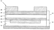
図1を見ると、エッチング前の層12及び14を含む通常の半導体構造体10が示されている。構造体10は、導電体18(例えば、銅(Cu)又はアルミニウム(Al)の)を囲む誘電体層16(例えば、二酸化シリコン(SiO2)の)を含む導電体層14と、導電体層14の上のキャップ層20(例えば、窒化チタン(TiN)の)と、キャップ層20の上の誘電体層22(例えば、二酸化シリコン(SiO2)の)と、誘電体層22の上の別の誘電体層24(例えば、窒化シリコン(Si3N4)の)と、パターン付けされたフォトレジスト26とを有する。
Turning to FIG. 1, a
典型的なRIE工程は、例えば、凡そ2MHz(底部RF電源電極)及び凡そ27MHz(上部バイアス電力電極)の二つのRF設定が可能な単一のプラズマ・チャンバ内で実施される。厚さ6μmのフォトレジスト26(例えば、Gpoly)と、厚さ4000Åの窒化シリコンの誘電体層24と、厚さ4500Åの二酸化シリコンの誘電体層22と、厚さ250−350Åの窒化チタンのキャップ層20とを有する積層に対する一つの通常のRIE工程をここで説明する。通常のRIE工程は、デスカム処理を実行するステップと、誘電体層24をエッチングするステップと、アルゴン(Ar)、テトラフルオロメタン(CF4)及び一酸化炭素(CO)を用いて誘電体層22をエッチングするステップと、キャップ層20を2段階エッチングするステップとを含む。第1のキャップ層エッチング・ステップには、アルゴン(Ar)、オクタフルオロシクロブタン(C4F8)、酸素(O2)、及びトリフルオロメタン(CHF3)を用いることができ、第2のキャップ層エッチング・ステップには、アルゴン(Ar)及び三フッ化窒素(NF3)を用いることができる。最後に、酸素(O2)プラズマ化学処理(灰化)を実行して、導電体18から残留RIEポリマーを除去する。
A typical RIE process is performed in a single plasma chamber capable of two RF settings, for example, approximately 2 MHz (bottom RF power electrode) and approximately 27 MHz (top bias power electrode). A 6 μm thick photoresist 26 (eg, Gpoly), a 4000 N thick silicon nitride
誘電体エッチング装置内でTiNを除去するための通常のRIE工程は、多くの問題を抱えている。第1に、その工程は装置の劣化をもたらし、より具体的には、エッチング速度の低下、及び、次のRIE処理におけるエッチングの均一性の低下をもたらし、その結果、歩留りを減少させる。第2に、典型的なプラズマ工程はウェハの劣化をもたらす。例えば、上記の工程は、ウェハの切り口内における静電気放電(ESD)欠陥の増加を示している。この事態に対処する一つの方法は、誘電体エッチング方式ではなく、金属エッチング方式を利用することである。しかし、これらの方式は、キャップ層20(窒化チタン)の下に残存する、例えば、アルミニウム(Al)の導電体18の形状に欠陥を生じる。即ち、その方式はアルミニウム(Al)に対しては選択できない。
The normal RIE process for removing TiN in a dielectric etching apparatus has many problems. First, the process results in device degradation, and more specifically, lower etch rates and etch uniformity in subsequent RIE processes, thereby reducing yield. Second, typical plasma processes result in wafer degradation. For example, the above process has shown an increase in electrostatic discharge (ESD) defects within the wafer cut. One way to deal with this situation is to use a metal etch rather than a dielectric etch. However, these methods cause defects in the shape of, for example, the aluminum (Al)
上述の状況に鑑みて、当技術分野において関連技術による問題のない改善されたRIE工程が要求されている。 In view of the above situation, there is a need in the art for an improved RIE process that is free of problems with the related art.
本発明は、導電体上の誘電体層及びキャップ層をエッチングして導電体を露出させる方法を含む。一つの実施形態においては、本方法には、オクタフルオロシクロブタン(C4F8)を含む二酸化シリコン(SiO2)エッチング化学処理剤、及びテトラフルオロメタン(CF4)を含む窒化チタン(TiN)エッチング化学処理剤を用いることが含まれる。本工程は、エッチング速度の低下を防ぎ、低減されたESD欠陥を示す。 The present invention includes a method of exposing a conductor by etching a dielectric layer and a cap layer on the conductor. In one embodiment, the method includes a silicon dioxide (SiO 2 ) etch chemistry comprising octafluorocyclobutane (C 4 F 8 ) and a titanium nitride (TiN) etch comprising tetrafluoromethane (CF 4 ). Use of chemical treatment agents is included. This step prevents the etch rate from decreasing and shows reduced ESD defects.
本発明の第1の態様は、導電体を露出させるエッチング法に向けられ、その方法は、オクタフルオロシクロブタン(C4F8)を含む化学処理剤を用いて二酸化シリコン(SiO2)を含む第1の誘電体層を通してエッチングするステップと、テトラフルオロメタン(CF4)を含む化学処理剤を用いて窒化チタン(TiN)を含むキャップ層を通してエッチングするステップとを含んだ、導電体を露出させる方法である。 A first aspect of the present invention is directed to an etching method that exposes a conductor, which includes silicon dioxide (SiO 2 ) using a chemical treating agent that includes octafluorocyclobutane (C 4 F 8 ). Etching through a dielectric layer and etching through a cap layer comprising titanium nitride (TiN) using a chemical treating agent comprising tetrafluoromethane (CF 4 ). It is.
本発明の第2の態様は、導電体を露出させるエッチング法を含み、その方法は、窒化シリコン(Si3N4)を含む第1の誘電体層を通してエッチングするステップと、オクタフルオロシクロブタン(C4F8)の凡そ13−17標準立法センチメートル(sccm)の気体流を含む化学処理剤を用いて二酸化シリコン(SiO2)を含む第2の誘電体層を通してエッチングするステップと、テトラフルオロメタン(CF4)の凡そ135−165sccmの気体流を含む化学処理剤を用いて窒化チタン(TiN)を含むキャップ層を通してエッチングするステップとを含んだ、導電体を露出させる方法である。 A second aspect of the present invention includes an etching method that exposes a conductor, the method comprising etching through a first dielectric layer comprising silicon nitride (Si 3 N 4 ), and octafluorocyclobutane (C Etching through a second dielectric layer comprising silicon dioxide (SiO 2 ) with a chemical treatment comprising a gas stream of approximately 13-17 standard cubic centimeters (sccm) of 4 F 8 ), tetrafluoromethane Etching through a cap layer comprising titanium nitride (TiN) using a chemical treating agent comprising a gas flow of approximately 135-165 sccm of (CF 4 ).
本発明の第3の態様は、窒化チタン(TiN)キャップ層と、その上の二酸化シリコン(SiO2)層と、その上の窒化シリコン(Si3N4)層と、その上のパターン付けされたフォトレジストとを有する積層の下の導電体を露出させる方法に関し、その方法は、窒化シリコン(Si3N4)層を通してエッチングするステップと、以下の諸条件、即ち、凡そ90−110mTorr(mT)の圧力と、凡そ27MHz及び凡そ2MHzにおける凡そ950−1050ワット(W)のRFエネルギーと、並びに、凡そ375−425sccmのアルゴン(Ar)、凡そ13−17sccmのオクタフルオロシクロブタン(C4F8)及び凡そ5−7sccmの酸素(O2)からなる気体流と、の条件を用いて二酸化シリコン(SiO2)層を通してエッチングするステップと、以下の諸条件、即ち、凡そ255−285mTorrの圧力と、凡そ27MHzにおける凡そ1350−1450W及び凡そ2MHzにおける凡そ650−750ワットのRFエネルギーと、並びに、凡そ135−165sccmのテトラフルオロメタン(CF4)及び凡そ90−110sccmの窒素(N2)の気体流と、の条件を用いて窒化チタン(TiN)を含む窒化チタン層を通してエッチングするステップとを含む。 A third aspect of the present invention is a titanium nitride (TiN) cap layer, a silicon dioxide (SiO 2 ) layer thereon, a silicon nitride (Si 3 N 4 ) layer thereon, and a patterned thereon. A method of exposing an underlying conductor with a photoresist layer comprising etching through a silicon nitride (Si 3 N 4 ) layer and the following conditions: approximately 90-110 mTorr (mT ), RF energy of approximately 950-1050 watts (W) at approximately 27 MHz and approximately 2 MHz, and approximately 375-425 sccm of argon (Ar), approximately 13-17 sccm of octafluorocyclobutane (C 4 F 8 ). And a gas flow consisting of approximately 5-7 sccm of oxygen (O 2 ) and silicon dioxide (S etching through the iO 2 ) layer, the following conditions: pressure of approximately 255-285 mTorr, RF energy of approximately 1350-1450 W at approximately 27 MHz and approximately 650-750 watts at approximately 2 MHz, and approximately 135 and a step of etching through the titanium nitride layer comprising titanium nitride (TiN) using a gas flow of -165sccm tetrafluoromethane (CF 4) and approximately 90-110sccm nitrogen (N 2), a condition.
本発明の前述及び他の特徴は、本発明の実施形態に関する以下のより詳細な説明から明瞭となるであろう。 The foregoing and other features of the present invention will become apparent from the following more detailed description of embodiments of the present invention.
本発明の実施形態は、以下の図面を参照しながら詳細に説明されるが、そこでは同様の符号は同様の要素を示す。 Embodiments of the present invention will be described in detail with reference to the following drawings, wherein like numerals indicate like elements.
本発明の図面は、一定の尺度で描かれてはいないことに注意されたい。図面は、本発明の典型的な態様を示すだけのものであり、従って、本発明の範囲を限定するものとは考えてはならない。図面において、図面間で同じ番号付けは同じ要素を表す。 It should be noted that the drawings of the present invention are not drawn to scale. The drawings show only typical embodiments of the invention and therefore should not be considered as limiting the scope of the invention. In the drawings, like numbering represents like elements between the drawings.
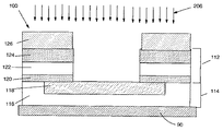
添付の図面に関して、図2−図6は、本発明による導電体を露出させる開口を形成するためのエッチング法の一つの実施形態を示す。開口のパターンはフォトレジストによって与えられる。本方法では、通常の方法を修正して静電気放電(ESD)欠陥を低減し、エッチング速度を低下させないようにする。本工程は、典型的な誘電体反応性イオン・エッチング(RIE)装置内で実施され、金属RIE装置は用いない。用いられるRIEチャンバは、例えば、凡そ2MHz(底部RF電源電極)及び凡そ27MHz(上部バイアス電力電極)の二つのRF設定が可能なものである。 With reference to the accompanying drawings, FIGS. 2-6 illustrate one embodiment of an etching method for forming an opening exposing a conductor according to the present invention. The pattern of openings is given by photoresist. In this method, the normal method is modified to reduce electrostatic discharge (ESD) defects and not to reduce the etch rate. This process is performed in a typical dielectric reactive ion etching (RIE) apparatus and does not use a metal RIE apparatus. The RIE chamber used is capable of two RF settings, for example, approximately 2 MHz (bottom RF power electrode) and approximately 27 MHz (top bias power electrode).
本工程は、図1に示されたものに類似した、誘電体層112を含む積層(大ビア・パッド積層とよばれることもある)を有する通常の半導体構造体100から開始する。構造体100は、導電体118(例えば、銅(Cu)又はアルミニウム(Al)の)を取り囲む誘電体層116(例えば、二酸化シリコン(SiO2)又は任意の他の適切な誘電体材料の)を含む導電体層114を有する。導電体118の上の積層は、導電体層114の上の窒化チタン(TiN)を含むキャップ層120と、キャップ層120の上の二酸化シリコン(SiO2)を含む誘電体層122と、誘電体層122の上の窒化シリコン(Si3N4)を含む別の誘電体層124と、パターン付けされたフォトレジスト126とを含む。パターン付けされたフォトレジスト126は、導電体118を露出するために形成されるべき開口のパターンを含む。誘電体層122は、水素化シリコンオキシカーバイド(SiCOH)、Novellus社から入手可能なCORAL(登録商標)、テトラエチルオルトシリケート(Si(OC2H5)4)(TEOS)、フッ素ドープTEOS(FTEOS)、フッ素ドープ・シリケート・ガラス(FSG)、非ドープ・シリケート・ガラス(USG)、ホウリン酸シリケート・ガラス(BPSG)などの任意の二酸化シリコン(SiO2)型材料を含むことができる。キャップ層120は、任意の典型的な窒化チタン・ベースのキャップ材料を含むことができる。
The process begins with a
本発明は、6μmのフォトレジスト12(例えばGpoly)と、4000Åの窒化シリコンの誘電体層124と、4500Åの二酸化シリコンを含む誘電体層122と、250−350Åの窒化チタン(TiN)を含むキャップ層120との厚さを有する積層に関して説明される。積層の厚さが変化するところでは、少なくともエッチング時間を適切に変化させ得ることを理解されたい。
The present invention includes a 6 μm photoresist 12 (eg, Gpoly), a
本方法の初めのステップは、図2に示されるように、デスカム処理200を実行することを含む。デスカム処理を実行するステップは、エッチングに先立ってリソグラフ・ステップからの残留物を除去し、これにより窒化シリコン表面のより均一なエッチングを可能にする。一つの実施形態においては、デスカム処理は窒素(N2)及び水素(H2)の気体流を用いて実行される。本説明において、「凡そX−Y」という用語が用いられる。この「凡そ」は、その範囲の下限値と上限値とに適用されるものと理解されたい。デスカム処理を実行するステップは、凡そ8−12秒の間継続することができる。デスカム処理を実行するステップにはまた、ヘリウム(He)による凡そ18−22Torrのウェハ保持チャック90(図2−図6)の圧力、及び、凡そ18−22℃のチャック温度の付加的な条件を用いることが含まれてもよい。
The initial steps of the method include performing a
図3に示されるように、次のステップは、例えば窒化シリコンの誘電体層124を通してエッチング202を行うことである。エッチング202の条件は、任意の通常の方法であってよい。例えば、エッチング202の条件には、アルゴン(Ar)、テトラフルオロメタン(CF4)、トリフルオロメタン(CHF3)及び酸素(O2)の気体流を用いることが含まれてよい。トリフルオロメタン(CHF3)(フルオロフォルムとしても知られている)は、例えば、フレオン(登録商標)23という商品名でデュポン社から入手できる。エッチング202は、凡そ40−50秒間継続することができる。チャック90の圧力は、例えば、ヘリウム(He)による凡そ18−20Torrとし、チャック90の温度は凡そ18−20℃とすることができる。
As shown in FIG. 3, the next step is to perform an
次に、図4に示されるように、二酸化シリコン(SiO2)を含む誘電体層122がエッチングされる。一つの実施形態においては、エッチング204の化学処理には、以下の諸条件、即ち、凡そ90−110mTorr(mT)の圧力と、凡そ27MHz及び凡そ2MHzにおける凡そ950−1050ワット(W)のRFエネルギーと、並びに、凡そ375−425sccmのアルゴン(Ar)、凡そ13−17sccmのオクタフルオロシクロブタン(C4F8)及び凡そ5−7sccmの酸素(O2)からなる気体流と、の条件を用いることが含まれる。エッチング204は、凡そ80−95秒間継続することができる。エッチング204にはまた、ヘリウム(He)による凡そ18−22Torrのウェハ保持チャック90の圧力、及び、凡そ18−22℃のチャック温度の条件を用いることもできる。
Next, as shown in FIG. 4, the
図5を参照すると、次のステップは、窒化チタン(TiN)を含んだキャップ層120をエッチングすることを含む。エッチング206では、以下の諸条件、即ち、凡そ255−285mTの圧力と、凡そ27MHzにおける凡そ1350−1450ワット(W)及び凡そ2MHzにおける凡そ650−750WのRFエネルギーと、並びに、凡そ135−165sccmのテトラフルオロメタン(CF4)及び凡そ90−110sccmの窒素(N2)からなる気体流と、の条件を用いることができる。エッチング206は凡そ85−100秒間継続することができる。エッチング206にはまた、ヘリウム(He)による凡そ18−22Torrのウェハ保持チャック90の圧力、及び、凡そ18−22℃のチャック温度の条件を用いることもできる。
Referring to FIG. 5, the next step includes etching the
図6は、導電体118から残留RIEポリマーを除去するための灰化ステップ208の実行を含む次のステップを示す。灰化実行ステップ208には、任意の現在既知の又は後に開発される酸素ベースの灰化化学処理剤を含めることができる。
FIG. 6 shows the next step including performing an
上述の発明は、二酸化シリコン(SiO2)及び窒化チタン(TiN)をエッチングするための2段階工程を提供する。本工程は、アルミニウム(Al)に対して選択的なものであり、従来のRIE工程と比べて、より少量のフォトレジスト126を消費する。本方法は、従来の方法を変更して、静電気放電(ESD)欠陥が低減され、エッチング速度が低下しないようにしたものである。更に、本工程は、典型的な誘電体反応性イオン・エッチング装置内で実行され、即ち、金属エッチング装置は用いない。
The above-described invention provides a two-step process for etching silicon dioxide (SiO 2 ) and titanium nitride (TiN). This process is selective to aluminum (Al) and consumes a smaller amount of
本発明は、上に概観された特定の実施形態に関連して説明されているが、明らかに、多くの代替、変更及び改変が当業者には明白であろう。従って、上に示された本発明の実施形態は、説明のためであって、限定のためではない。添付の請求項によって規定される本発明の精神と範囲から逸脱することなしに、種々の変更を施すことが可能である。 Although the present invention has been described in connection with the specific embodiments outlined above, many alternatives, modifications and variations will be apparent to those skilled in the art. Accordingly, the embodiments of the invention shown above are for purposes of illustration and not limitation. Various changes may be made without departing from the spirit and scope of the invention as defined by the appended claims.
10,100:半導体構造体
12,112:誘電体層を含む積層
14,114:導電体を含む層
16,22、24、116、122、124:誘電体層
18,118:導電体
20,120:キャップ層
26、126:フォトレジスト
200:デスカム処理
202、204、206:エッチング
208:灰化
DESCRIPTION OF SYMBOLS 10,100: Semiconductor structure 12,112: Lamination | stacking 14 including a dielectric layer, 114:
Claims (20)
オクタフルオロシクロブタン(C4F8)を含む化学処理剤を用いて二酸化シリコン(SiO2)を含む第1の誘電体層を通してエッチングするステップと、
テトラフルオロメタン(CF4)を含む化学処理剤を用いて窒化チタン(TiN)を含むキャップ層を通してエッチングして、前記導電体を露出するステップと
を含む方法。 An etching method for exposing a conductor, the method comprising:
Etching through a first dielectric layer comprising silicon dioxide (SiO 2 ) with a chemical treating agent comprising octafluorocyclobutane (C 4 F 8 );
Etching through a cap layer comprising titanium nitride (TiN) with a chemical treating agent comprising tetrafluoromethane (CF 4 ) to expose the conductor.
窒化シリコン(Si3N4)を含む第1の誘電体層を通してエッチングするステップと、
13−17標準立法センチメートル(sccm)のオクタフルオロシクロブタン(C4F8)の気体流を含む化学処理剤を用いて二酸化シリコン(SiO2)を含む第2の誘電体層を通してエッチングするステップと、
135−165sccmのテトラフルオロメタン(CF4)の気体流を含む化学処理剤を用いて窒化チタン(TiN)を含むキャップ層を通してエッチングして、導電体を露出するステップと
を含む方法。 An etching method for exposing a conductor, the method comprising:
Etching through a first dielectric layer comprising silicon nitride (Si 3 N 4 );
And etching through the second dielectric layer including silicon dioxide (SiO 2) using a 13-17 chemical treatment agent comprising a gas flow octafluorocyclobutane standard cubic centimeters (sccm) (C 4 F 8 ) ,
Etching through a cap layer comprising titanium nitride (TiN) with a chemical treating agent comprising a gas flow of 135-165 sccm of tetrafluoromethane (CF 4 ) to expose the conductor.
窒化シリコン(Si3N4)層を通してエッチングするステップと、
90−110mTorr(mT)の圧力と、27MHz及び2MHzにおける950−1050ワット(W)のRFエネルギーと、375−425sccmのアルゴン(Ar)、13−17sccmのオクタフルオロシクロブタン(C4F8)及び5−7sccmの酸素(O2)からなる気体流と、の条件を用いて、二酸化シリコン(SiO2)層を通してエッチングするステップと、
255−285mTの圧力と、27MHzにおける1350−1450W及び2MHzにおける650−750WのRFエネルギーと、135−165sccmのテトラフルオロメタン(CF4)及び90−110sccmの窒素(N2)からなる気体流と、の条件を用いて、窒化チタン(TiN)層を通してエッチングするステップと
を含む方法。 Under the stack comprising a titanium nitride (TiN) cap layer, a silicon dioxide (SiO 2 ) layer thereon, a silicon nitride (Si 3 N 4 ) layer thereon, and a patterned photoresist thereon A method of exposing a conductor in the method, the method comprising:
Etching through a silicon nitride (Si 3 N 4 ) layer;
90-110 mTorr (mT) pressure, 950-1050 Watt (W) RF energy at 27 MHz and 2 MHz, 375-425 sccm Argon (Ar), 13-17 sccm Octafluorocyclobutane (C 4 F 8 ) and 5 Etching through a silicon dioxide (SiO 2 ) layer using a gas flow comprising −7 sccm of oxygen (O 2 ), and
A gas flow consisting of a pressure of 255-285 mT, RF energy of 1350-1450 W at 27 MHz and 650-750 W at 2 MHz, 135-165 sccm of tetrafluoromethane (CF 4 ) and 90-110 sccm of nitrogen (N 2 ); Etching through a titanium nitride (TiN) layer using the conditions of:
Applications Claiming Priority (1)
| Application Number | Priority Date | Filing Date | Title |
|---|---|---|---|
| US11/163,836 US7276450B2 (en) | 2005-11-01 | 2005-11-01 | Etching processes using C4F8 for silicon dioxide and CF4 for titanium nitride |
Publications (2)
| Publication Number | Publication Date |
|---|---|
| JP2007129219A true JP2007129219A (en) | 2007-05-24 |
| JP2007129219A5 JP2007129219A5 (en) | 2008-12-11 |
Family
ID=37994900
Family Applications (1)
| Application Number | Title | Priority Date | Filing Date |
|---|---|---|---|
| JP2006293192A Pending JP2007129219A (en) | 2005-11-01 | 2006-10-27 | Etching process using c4f8 for silicon dioxide and cf4 for titanium nitride |
Country Status (3)
| Country | Link |
|---|---|
| US (1) | US7276450B2 (en) |
| JP (1) | JP2007129219A (en) |
| CN (1) | CN1967777A (en) |
Families Citing this family (11)
| Publication number | Priority date | Publication date | Assignee | Title |
|---|---|---|---|---|
| JP5309601B2 (en) | 2008-02-22 | 2013-10-09 | 富士通セミコンダクター株式会社 | Manufacturing method of semiconductor device |
| US20110174774A1 (en) * | 2010-01-21 | 2011-07-21 | Ying-Chih Lin | Method of descumming patterned photoresist |
| US20120289043A1 (en) * | 2011-05-12 | 2012-11-15 | United Microelectronics Corp. | Method for forming damascene trench structure and applications thereof |
| US8772558B2 (en) | 2011-07-26 | 2014-07-08 | Uop Llc | Methods and apparatuses for producing aromatic hydrocarbon-containing effluent |
| US9059250B2 (en) | 2012-02-17 | 2015-06-16 | International Business Machines Corporation | Lateral-dimension-reducing metallic hard mask etch |
| US8999184B2 (en) * | 2012-08-03 | 2015-04-07 | Lam Research Corporation | Method for providing vias |
| US9269678B2 (en) * | 2012-10-25 | 2016-02-23 | United Microelectronics Corp. | Bond pad structure and method of manufacturing the same |
| US9287109B2 (en) * | 2013-03-13 | 2016-03-15 | Globalfoundries Inc. | Methods of forming a protection layer to protect a metal hard mask layer during lithography reworking processes |
| RU2533740C1 (en) * | 2013-07-04 | 2014-11-20 | Федеральное государственное автономное образовательное учреждение высшего профессионального образования "Национальный исследовательский университет "МИЭТ" (МИЭТ) | Method for reactive ion etching of titanium nitride layer selectively to silicon dioxide, polysilicon and tungsten |
| CN104882408A (en) * | 2015-05-20 | 2015-09-02 | 中国航天科技集团公司第九研究院第七七一研究所 | Through hole etching method for reducing hole-chain resistance between multilayer metals of integrated circuit |
| CN105977149A (en) * | 2016-05-11 | 2016-09-28 | 上海华虹宏力半导体制造有限公司 | Passivation layer etching method, manufacture method of pad and manufacture method of semiconductor device |
Family Cites Families (16)
| Publication number | Priority date | Publication date | Assignee | Title |
|---|---|---|---|---|
| US5419805A (en) | 1992-03-18 | 1995-05-30 | Northern Telecom Limited | Selective etching of refractory metal nitrides |
| US5930664A (en) * | 1997-07-24 | 1999-07-27 | Taiwan Semiconductor Manufacturing Company, Ltd. | Process for preventing corrosion of aluminum bonding pads after passivation/ARC layer etching |
| US6297167B1 (en) | 1997-09-05 | 2001-10-02 | Advanced Micro Devices, Inc. | In-situ etch of multiple layers during formation of local interconnects |
| US20020076935A1 (en) | 1997-10-22 | 2002-06-20 | Karen Maex | Anisotropic etching of organic-containing insulating layers |
| US6214742B1 (en) * | 1998-12-07 | 2001-04-10 | Advanced Micro Devices, Inc. | Post-via tin removal for via resistance improvement |
| US6096579A (en) * | 1999-03-25 | 2000-08-01 | Vanguard International Semiconductor Corporation | Method for controlling the thickness of a passivation layer on a semiconductor device |
| US6383945B1 (en) | 1999-10-29 | 2002-05-07 | Advanced Micro Devices, Inc. | High selectivity pad etch for thick topside stacks |
| US6284657B1 (en) * | 2000-02-25 | 2001-09-04 | Chartered Semiconductor Manufacturing Ltd. | Non-metallic barrier formation for copper damascene type interconnects |
| US6479411B1 (en) * | 2000-03-21 | 2002-11-12 | Angela T. Hui | Method for forming high quality multiple thickness oxide using high temperature descum |
| US6890863B1 (en) | 2000-04-27 | 2005-05-10 | Micron Technology, Inc. | Etchant and method of use |
| US6350700B1 (en) * | 2000-06-28 | 2002-02-26 | Lsi Logic Corporation | Process for forming trenches and vias in layers of low dielectric constant carbon-doped silicon oxide dielectric material of an integrated circuit structure |
| US6531404B1 (en) * | 2000-08-04 | 2003-03-11 | Applied Materials Inc. | Method of etching titanium nitride |
| US6746961B2 (en) * | 2001-06-19 | 2004-06-08 | Lam Research Corporation | Plasma etching of dielectric layer with etch profile control |
| US6713402B2 (en) | 2002-05-31 | 2004-03-30 | Texas Instruments Incorporated | Methods for polymer removal following etch-stop layer etch |
| KR100540475B1 (en) | 2003-04-04 | 2006-01-10 | 주식회사 하이닉스반도체 | Method for fabrication of semiconductor device capable of forming fine pattern |
| JP2006024811A (en) * | 2004-07-09 | 2006-01-26 | Sony Corp | Method for manufacturing semiconductor device |
-
2005
- 2005-11-01 US US11/163,836 patent/US7276450B2/en not_active Expired - Fee Related
-
2006
- 2006-09-13 CN CNA2006101542027A patent/CN1967777A/en active Pending
- 2006-10-27 JP JP2006293192A patent/JP2007129219A/en active Pending
Also Published As
| Publication number | Publication date |
|---|---|
| CN1967777A (en) | 2007-05-23 |
| US7276450B2 (en) | 2007-10-02 |
| US20070095787A1 (en) | 2007-05-03 |
Similar Documents
| Publication | Publication Date | Title |
|---|---|---|
| JP2007129219A (en) | Etching process using c4f8 for silicon dioxide and cf4 for titanium nitride | |
| US7265060B2 (en) | Bi-level resist structure and fabrication method for contact holes on semiconductor substrates | |
| JP5134363B2 (en) | Substrate etching by plasma processing system | |
| JP5178983B2 (en) | Method for etching dual damascene structures in organosilicate glass | |
| JP5183850B2 (en) | Method for stripping a photoresist from a semiconductor wafer having a layer of an organosilicate dielectric | |
| EP1012877A1 (en) | Method for selective plasma etch | |
| WO2002065528A2 (en) | Use of ammonia for etching organic low-k dielectrics | |
| JP2006013190A (en) | Method of manufacturing semiconductor device | |
| US6187666B1 (en) | CVD plasma process to fill contact hole in damascene process | |
| US5792672A (en) | Photoresist strip method | |
| US6271115B1 (en) | Post metal etch photoresist strip method | |
| US7199059B2 (en) | Method for removing polymer as etching residue | |
| US20060276031A1 (en) | Method for forming via-hole in semiconductor device | |
| KR100512904B1 (en) | Fabricating method for semiconductor device | |
| US7510965B2 (en) | Method for fabricating a dual damascene structure | |
| US6803307B1 (en) | Method of avoiding enlargement of top critical dimension in contact holes using spacers | |
| JP2003332337A (en) | Manufacturing method of semiconductor device | |
| US7045464B1 (en) | Via reactive ion etching process | |
| US7265053B2 (en) | Trench photolithography rework for removal of photoresist residue | |
| US7172959B2 (en) | Method for forming dual damascene interconnection in semiconductor device | |
| JP2006032721A (en) | Fabrication process of semiconductor device | |
| JP2006156591A (en) | Method for manufacturing semiconductor device | |
| KR20040077272A (en) | Method of etching silicon nitride film | |
| KR100332647B1 (en) | Method of forming a contact hole in a semiconductor device | |
| KR100620711B1 (en) | Method for Forming Contact Hole Capable of Removing Polymer and Method for Manufacturing Semiconductor Device Using the Contact Hole Forming Method |
Legal Events
| Date | Code | Title | Description |
|---|---|---|---|
| A521 | Request for written amendment filed |
Free format text: JAPANESE INTERMEDIATE CODE: A523 Effective date: 20081028 |
|
| A621 | Written request for application examination |
Free format text: JAPANESE INTERMEDIATE CODE: A621 Effective date: 20081028 |
|
| A871 | Explanation of circumstances concerning accelerated examination |
Free format text: JAPANESE INTERMEDIATE CODE: A871 Effective date: 20081028 |
|
| A975 | Report on accelerated examination |
Free format text: JAPANESE INTERMEDIATE CODE: A971005 Effective date: 20081113 |
|
| A977 | Report on retrieval |
Free format text: JAPANESE INTERMEDIATE CODE: A971007 Effective date: 20090223 |
|
| A131 | Notification of reasons for refusal |
Free format text: JAPANESE INTERMEDIATE CODE: A131 Effective date: 20090407 |
|
| A02 | Decision of refusal |
Free format text: JAPANESE INTERMEDIATE CODE: A02 Effective date: 20090929 |