JP2007123785A - Variable inductor and antenna device using it - Google Patents
Variable inductor and antenna device using it Download PDFInfo
- Publication number
- JP2007123785A JP2007123785A JP2005317646A JP2005317646A JP2007123785A JP 2007123785 A JP2007123785 A JP 2007123785A JP 2005317646 A JP2005317646 A JP 2005317646A JP 2005317646 A JP2005317646 A JP 2005317646A JP 2007123785 A JP2007123785 A JP 2007123785A
- Authority
- JP
- Japan
- Prior art keywords
- inductor
- variable inductor
- coil conductor
- main
- conductor
- Prior art date
- Legal status (The legal status is an assumption and is not a legal conclusion. Google has not performed a legal analysis and makes no representation as to the accuracy of the status listed.)
- Pending
Links
- 238000003475 lamination Methods 0.000 claims abstract description 23
- 230000008878 coupling Effects 0.000 claims abstract description 13
- 238000010168 coupling process Methods 0.000 claims abstract description 13
- 238000005859 coupling reaction Methods 0.000 claims abstract description 13
- 239000004020 conductor Substances 0.000 claims description 170
- 239000003990 capacitor Substances 0.000 claims description 9
- 238000004804 winding Methods 0.000 claims description 9
- 238000010030 laminating Methods 0.000 claims 1
- 230000000694 effects Effects 0.000 description 16
- 239000010410 layer Substances 0.000 description 15
- 230000008859 change Effects 0.000 description 4
- 239000000463 material Substances 0.000 description 3
- 239000000919 ceramic Substances 0.000 description 2
- 229910052802 copper Inorganic materials 0.000 description 2
- 230000006866 deterioration Effects 0.000 description 2
- 238000010586 diagram Methods 0.000 description 2
- 230000006872 improvement Effects 0.000 description 2
- 230000003993 interaction Effects 0.000 description 2
- 229910052759 nickel Inorganic materials 0.000 description 2
- 229910052709 silver Inorganic materials 0.000 description 2
- 229910004298 SiO 2 Inorganic materials 0.000 description 1
- XUIMIQQOPSSXEZ-UHFFFAOYSA-N Silicon Chemical compound [Si] XUIMIQQOPSSXEZ-UHFFFAOYSA-N 0.000 description 1
- 229910007565 Zn—Cu Inorganic materials 0.000 description 1
- PNEYBMLMFCGWSK-UHFFFAOYSA-N aluminium oxide Inorganic materials [O-2].[O-2].[O-2].[Al+3].[Al+3] PNEYBMLMFCGWSK-UHFFFAOYSA-N 0.000 description 1
- 230000003247 decreasing effect Effects 0.000 description 1
- 230000010355 oscillation Effects 0.000 description 1
- 230000002093 peripheral effect Effects 0.000 description 1
- 239000011347 resin Substances 0.000 description 1
- 229920005989 resin Polymers 0.000 description 1
- 239000004065 semiconductor Substances 0.000 description 1
- 229910052710 silicon Inorganic materials 0.000 description 1
- 239000010703 silicon Substances 0.000 description 1
- 239000002356 single layer Substances 0.000 description 1
- 239000000758 substrate Substances 0.000 description 1
- 229910000859 α-Fe Inorganic materials 0.000 description 1
Images


Classifications
-
- H—ELECTRICITY
- H01—ELECTRIC ELEMENTS
- H01F—MAGNETS; INDUCTANCES; TRANSFORMERS; SELECTION OF MATERIALS FOR THEIR MAGNETIC PROPERTIES
- H01F21/00—Variable inductances or transformers of the signal type
- H01F21/12—Variable inductances or transformers of the signal type discontinuously variable, e.g. tapped
- H01F2021/125—Printed variable inductor with taps, e.g. for VCO
Landscapes
- Engineering & Computer Science (AREA)
- Power Engineering (AREA)
- Coils Or Transformers For Communication (AREA)
Abstract
Description
本発明は、可変インダクタ及びそれを利用したアンテナ装置に関し、更に具体的には、インダクタンスの可変幅の改善に関するものである。 The present invention relates to a variable inductor and an antenna device using the variable inductor, and more specifically to improvement of a variable width of inductance.
電子機器に使用される個々の部品偏差を吸収したり、回路に組み込んだ後にそのインダクタンスを調整したりするものとして、インダクタンス値の変更が可能な可変インダクタがあり、各種のものが提案されている。例えば、以下の特許文献1には、平面スパイラル状の主コイル(第1導体)の各周回部に対向するように、開放端間にスイッチが接続された単一周回調整用コイル(第2導体)を複数配置した可変インダクタ及びそれを利用した半導体集積回路が開示されている。また、特許文献2には、シリコン基板上に主コイル導体(主インダクタ)と調整用コイル導体(副インダクタ)とを同軸で内外に隣接配置し、調整用コイル導体の端部をスイッチで開閉自在にした電圧制御発振回路が開示されている。
しかしながら、以上のような背景技術は、高周波(100MHz以上)ではスイッチの影響が小さいものの、主コイル導体と調整用コイル導体との結合度が十分ではないため、主コイルのインダクタンス値の可変幅が狭いという不都合がある。 However, although the background art as described above is less affected by the switch at high frequencies (100 MHz or higher), the degree of coupling between the main coil conductor and the adjustment coil conductor is not sufficient, so that the variable width of the inductance value of the main coil is small. There is an inconvenience of being narrow.
本発明は、以上の点に着目したもので、その目的は、主コイルのQ値を低下させることなく、インダクタンス値の可変幅を広げることができる可変インダクタを提供することである。他の目的は、前記可変インダクタを利用したアンテナ装置を提供することである。 The present invention focuses on the above points, and an object thereof is to provide a variable inductor capable of widening the variable range of the inductance value without reducing the Q value of the main coil. Another object is to provide an antenna device using the variable inductor.
前記目的を達成するため、本発明の可変インダクタは、積層体の内部に積層方向に沿って巻回された主コイル導体と、該主コイル導体と対向するように前記積層体の内部に配置された調整用コイル導体と、前記積層体表面に設けられており、前記各コイル導体の端部が接続される端子電極と、前記調整用コイル導体の端部が接続された一対の端子電極間に、前記積層体の外部で接続されたスイッチ素子と、を備えたことを特徴とする。 In order to achieve the above object, a variable inductor according to the present invention is arranged inside a multilayer body so as to face the main coil conductor, and a main coil conductor wound in the lamination direction inside the multilayer body. A coil conductor for adjustment, provided on the surface of the laminate, a terminal electrode to which an end portion of each coil conductor is connected, and a pair of terminal electrodes to which an end portion of the adjustment coil conductor is connected And a switch element connected outside the laminate.
本発明のアンテナ装置は、請求項1〜8のいずれかに記載の可変インダクタを利用したことを特徴とする。本発明の前記目的,特徴,利点は、以下の詳細な説明及び添付図面から明瞭になろう。
An antenna device according to the present invention uses the variable inductor according to any one of
本発明は、積層体内部に積層方向に沿って巻回された主コイル導体に対して、調整用コイル導体を積層体内で対向配置し、各コイル導体の端部を積層体表面の端子電極に接続するとともに、前記調整用コイル導体端部に接続する一対の端子電極間に、積層体外部でスイッチ素子を接続することとした。このため、主コイル導体にスイッチ素子が直接接続されないのでQ値の劣化を抑制しつつ、主コイル導体と調整用コイル導体との結合度を高めて、主コイル導体のインダクタンスの可変幅を広げるという効果が得られる。 In the present invention, an adjustment coil conductor is disposed opposite to a main coil conductor wound in the stacking direction in the stack within the stack, and the end of each coil conductor is used as a terminal electrode on the surface of the stack. In addition to the connection, the switch element is connected outside the laminated body between the pair of terminal electrodes connected to the end of the adjustment coil conductor. For this reason, since the switching element is not directly connected to the main coil conductor, the degree of coupling between the main coil conductor and the adjustment coil conductor is increased and the variable width of the inductance of the main coil conductor is increased while suppressing the deterioration of the Q value. An effect is obtained.
以下、本発明を実施するための最良の形態を、実施例に基づいて詳細に説明する。 Hereinafter, the best mode for carrying out the present invention will be described in detail based on examples.
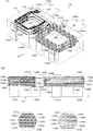
最初に、図1を参照しながら本発明の実施例1を説明する。図1(A)は、本実施例の可変インダクタのインダクタ配置(コイル配置)を示す斜視図であり、図1(B)は、前記(A)を矢印F1方向から見た側面図である。図1に示すように、本実施例の可変インダクタ10は、積層体12とスイッチ26を備えている。前記積層体12は、絶縁層を積層した積層体の内部に、メインインダクタ(主コイル導体)14と制御インダクタ(調整用コイル導体)18が隣接して対向配置された構成となっている。なお、理解を容易にするため、前記絶縁層は、図中から省略されている。また、積層体12の表面(側面)には、前記メインインダクタ14及び制御インダクタ18の端部が接続される端子電極22A〜22Fが、適宜位置に形成されている。更に、積層体12の底面には、端子電極22Bと22Eを短絡するとともに配線基板への実装時の特性変化を少なくするためのシールド層24が設けられている。
First,
前記メインインダクタ14は、複数の導体パターン14A〜14Gが、積層体12の積層方向に沿って巻回するように積層されており、これら導体パターン14A〜14Gは、スルーホール15A〜15Fによって接続されている。そして、メインインダクタ14の一方の端部16Aは、積層体12の表面の端子電極22Aに接続され、他方の端部16Bは、端子電極22Cに接続されている。同様に、制御インダクタ18も、複数の導体パターン18A〜18Gが積層方向に沿って巻回するように積層されており、これら導体パターン18A〜18Gは、スルーホール19A〜19Fによって接続されている。そして、制御インダクタ18の一方の端部20Aは、端子電極22Dに接続され、他方の端部20Bは、端子電極22Fに接続される。更に、これら端子電極22D及び22F間には、積層体12の外部で、スイッチ26が接続されている。なお、上述した導体パターン14A〜14G,18A〜18Gとしては、例えばAg,Ni,Cuなどが用いられ、端子電極22A〜22Fとしては、例えばAg,Ni,Cu,導電性樹脂などが用いられるが、他の公知の各種の材料を利用するようにしてもよい。可変インダクタ10を、以上のような構成にすることにより、メインインダクタ14にスイッチ等の余分な負荷を設けることなく、インダクタンス値を変更することができる。
The
このように、実施例1によれば、次のような効果がある。
(1)積層体12の内部に、その積層方向に沿って巻回したメインインダクタ14と制御インダクタ18を、隣接して対向配置することとしたので、結合度を向上させてインダクタンス値の可変量を大きくすることができる。
(2)メインインダクタ14にスイッチ26が直接接続されず、余分な負荷を設ける必要がないため、メインインダクタ14のQ値の劣化を抑制することができる。
Thus, according to the first embodiment, there are the following effects.
(1) Since the
(2) Since the
次に、図2を参照しながら本発明の実施例2を説明する。図2(A)は、本実施例の可変インダクタのインダクタ配置を示す斜視図であり、図2(B)は前記(A)を矢印F2方向から見た側面図である。なお、上述した実施例1と同一ないし対応する構成要素には同一の符号を用いることとする(以下の実施例1についても同様)。前記実施例1では、メインインダクタ14と制御インダクタ18を、単に積層方向に対向配置したが、本実施例では、図2に示すように、メインインダクタと制御インダクタの分割形成した導体パターンを、交互に積層した構成となっている。
Next,
詳細に説明すると、メインインダクタ14は、導体パターン14A〜14Gが、積層体12の積層方向に沿って巻回するように積層されており、これら導体パターン14A〜14Gは、スルーホール15A〜15Fによって接続されている。同様に、制御インダクタ18は、導体パターン18A〜18Gが、積層方向に沿って巻回するように積層されており、これら導体パターン18A〜18Gは、スルーホール19A〜19Fによって接続されている。そして、これらメインインダクタ14の導体パターン14A〜14Gと、制御インダクタ18の導体パターン18A〜18Gは、交互に積層される。図2に示す例では、積層体32の上側から、導体パターン14A,18A,14B,18B,14C,18C,14D,18D,14E,18E,14F,18F,14G,18Gとなるように配置されている。
More specifically, the
そして、メインインダクタ14の端部16A及び16Bは、それぞれ積層体32の表面の端子電極22A及び22Cに接続される。また、制御インダクタの端部20A及び20Bは、それぞれ端子電極22D及び22Fに接続され、これら端子電極22D及び22F間には、前記実施例1と同様にスイッチ26が接続される。本実施例の基本的作用・効果は、上述した実施例1と同様であるが、メインインダクタ14の導体パターンと、制御インダクタ18の導体パターンを交互に積層することとしたので、より結合度の向上を図ることができる。
The
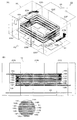
次に、図3を参照しながら本発明の実施例3を説明する。図3(A)は、本実施例の可変インダクタのインダクタ配置を示す斜視図であり、図3(B)は前記(A)を矢印F3方向から見た側面図である。上述した実施例1及び2では、一つのメインインダクタに対して、一つの制御インダクタを設けた例であるが、本実施例は、一つのメインインダクタに対して3つの制御インダクタを設けたものである。図3に示すように、本実施例の可変インダクタ40は、積層体42内に、メインインダクタ44と制御インダクタ48,54および62が対向配置されている。また、積層体42の表面には、前記メインインダクタ44及び制御インダクタ48,54,62の端部が接続される端子電極60A〜60Hが適宜位置に形成されている。
Next, Embodiment 3 of the present invention will be described with reference to FIG. FIG. 3 (A) is a perspective view showing the inductor arrangement of the variable inductor of this embodiment, and FIG. 3 (B) is a side view of (A) seen from the direction of arrow F3. In the first and second embodiments described above, one control inductor is provided for one main inductor, but in this embodiment, three control inductors are provided for one main inductor. is there. As shown in FIG. 3, in the
前記メインインダクタ44は、複数の導体パターン44A〜44Fが、積層体42の積層方向に沿って巻回するように積層されており、これら導体パターン44A〜44Fは、スルーホール46A〜46Eにより接続されている。そして、メインインダクタ44の一方の端部(導体パターン44A側)は、端子電極60Aに接続され、他方の端部(導体パターン44F側)は、端子電極60Eに接続されている。一方、制御インダクタ48は、導体パターン48A及び48Bが、積層方向に沿って巻回するように積層されて、スルーホール50により接続されている。前記導体パターン48A,48Bは、前記メインインダクタ44の導体パターン44Aを挟むように配置されている。そして、一方の端部(導体パターン48A側)が端子電極60Dに接続され、他方の端部(導体パターン48B側)は端子電極60Hに接続されている。更に、これら端子電極60D及び60F間には、積層体42の外部で、スイッチ64Aが接続されている。
The
また、制御インダクタ54は、導体パターン54A〜54Dが、積層方向に沿って巻回するように積層されており、スルーホール56A〜56Cにより接続されている。前記導体パターン54A〜54Dは、前記メインインダクタ44の導体パターン44B〜44Fと交互になるように積層されている。そして、一方の端部(導体パターン54A側)が端子電極60Gに接続され、他方の端部(導体パターン54D側)が端子電極60Fに接続されている。
更に、これら端子電極60F及び60G間には、積層体42の外部で、スイッチ64Bが接続されている。更に、制御インダクタ62は、略C字形の1ターンに満たない単一層の導体パターン62Aにより構成されており、該導体パターン62Aは、前記メインインダクタ44の導体パターン44Fに対向するように、その下側に配置されている。そして、一方の端部が端子電極60Bに接続され、他方の端部は、端子電極60Cに接続されている。そして、これらの端子電極60B及び60C間には、積層体42の外部で、スイッチ64Cが接続されている。
なお、上述した導体パターン44A〜44F,48A,48B,54A〜54D,62Aや、端子電極60A〜60Hとしては、上述した実施例1と同様の材料が用いられる。本実施例の作用・効果は、基本的には上述した実施例2と同様であるが、3つの制御インダクタ48,54,62をメインインダクタ44の上部,中間部及び下部に重なるように配置することとしたので、メインインダクタ44に対して異なる結合係数を得ることが可能となり、メインインダクタ44のインダクタンス値を所望の値に変化させることが可能となる。また、制御インダクタ48,54及び62のそれぞれの間にはメインインダクタ44の導体パターン44B及び44Fが配置されるので、それぞれの制御用インダクタ間の相互作用が抑制され、メインインダクタ44に対してそれぞれ独立して機能することができるという効果もある。
Further, the
Further, a
The
次に、図4を参照しながら本発明の実施例4を説明する。図4(A)は、本実施例の可変インダクタのインダクタ配置を示す斜視図であり、図4(B)は前記(A)を矢印F4方向から見た側面図である。上述した実施例3では、一つのメインインダクタに、上部,中間部,下部で重なるように3つの制御インダクタを設けたが、本実施例は、一つのメインインダクタの左右に重なるように2つの制御インダクタを配置した構成となっている。図4に示すように、本実施例の可変インダクタ70は、積層体72内に、メインインダクタ74と、該メインインダクタ74の一部と重なる2つの制御インダクタ80及び84が配置されている。また、積層体72の表面には、前記メインインダクタ74及び制御インダクタ80及び84の端部が接続される端子電極88A〜88Hが適宜位置に形成されている。
Next, Embodiment 4 of the present invention will be described with reference to FIG. FIG. 4A is a perspective view showing the inductor arrangement of the variable inductor of the present embodiment, and FIG. 4B is a side view of (A) seen from the direction of arrow F4. In the third embodiment described above, three control inductors are provided on one main inductor so as to overlap the upper, middle, and lower portions. However, in this embodiment, two controls are provided so as to overlap the left and right of one main inductor. The inductor is arranged. As shown in FIG. 4, in the
前記メインインダクタ74は、複数の導体パターン74A〜74Eが、積層体72の積層方向に沿って巻回するように積層されており、これら導体パターン74A〜74Eは、スルーホール76A〜76Dにより接続されている。そして、メインインダクタ74の一方の端部(導体パターン74A側)は、端子電極88Dに接続され、他方の端部(導体パターン74E側)は、端子電極88Aに接続されている。一方、制御インダクタ80は、導体パターン80A〜80Eが、積層方向に沿って巻回するように積層されて、スルーホール82A〜82Dにより接続されている。これら導体パターン82A〜82Eは、メインインダクタ74の一部(図示の例では左側)の導体パターン74A〜74Eと交互に重なり合うように積層配置されている。そして、一方の端部(導体パターン80A側)が端子電極88Eに接続され、他方の端部(導体パターン80E側)は端子電極88Fに接続されている。更に、これら端子電極88E及び88F間には、積層体72の外部で、スイッチ89Aが接続されている。
The
また、制御インダクタ84は、導体パターン84A〜84Fが、積層方向に沿って巻回するように積層されており、スルーホール86A〜86Eにより接続されている。前記導体パターン84A〜84Fは、前記メインインダクタ74の一部(図示の例では右側)の導体パターン74A〜74Eと交互に重なり合うように積層配置されている。そして、一方の端部(導体パターン84A側)が端子電極88Gに接続され、他方の端部(導体パターン84F側)が端子電極88Hに接続されている。更に、これら端子電極88G及び88H間には、積層体72の外部で、スイッチ89Bが接続されている。本実施例の作用・効果は、上述した実施例2と同様であるが、2つの制御インダクタ80及び84を、これらが積層方向で互いに重ならないようにメインインダクタ74に対向配置することとしたので、制御インダクタ間の相互作用をより確実に抑制することができるとともに、インダクタの結合の大きさがその対向面積で決まるため、メインインダクタ74のインダクタンス値の変化量の設計が容易になるという効果もある。また、スイッチ89A及び89Bが接続される端子電極が隣接しているため、外部に接続するスイッチへの回路設計が容易になるという効果もある。
The
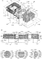
次に、図5を参照しながら本発明の実施例5を説明する。図5(A)は、本実施例の可変インダクタのインダクタ配置を示す斜視図であり、図5(B)は前記(A)を矢印F5方向から見た側面図である。上述した実施例4は、2つの制御インダクタを用いたものの、メインインダクタの巻回軸は一つであるが、本実施例は、メインインダクタが複数の巻回軸を備えた構成となっている。図5に示すように、本実施例の可変インダクタ90は、積層体91内に、3つのインダクタ部94,96,98を備えたメインインダクタ92と、前記各インダクタ部94,96,98と導体パターンが交互に重なる3つの制御インダクタ100,106,110が配置されている。また、積層体91の表面には、前記メインインダクタ92及び制御インダクタ100,106,110の端部が接続される端子電極114A〜114Hが適宜位置に形成されている。
Next, Embodiment 5 of the present invention will be described with reference to FIG. FIG. 5 (A) is a perspective view showing the inductor arrangement of the variable inductor of this embodiment, and FIG. 5 (B) is a side view of (A) seen from the direction of arrow F5. Although the above-described fourth embodiment uses two control inductors, the main inductor has one winding axis. However, in this embodiment, the main inductor has a plurality of winding axes. . As shown in FIG. 5, the
前記メインインダクタ92は、3つのインダクタ部94,96,98によって構成されている。インダクタ部94は、複数の導体パターン94A〜94Eが、積層体91の積層方向に沿って巻回するように積層されており、これら導体パターン94A〜94Eは、スルーホール95A〜95Dにより接続されている。同様に、インダクタ部96は、複数の導体パターン96A〜96Eがスルーホール97A〜97Dにより接続され、インダクタ部98は、複数の導体パターン98A〜98Fがスルーホール99A〜99Eにより接続されている。なお、前記インダクタ部94と96は、同一面上にある導体パターン94E及び96Eにより連続しており、インダクタ部96と98は、同一面上にある導体パターン96Aと98Aにより連続している。このようなメインインダクタ92の一方の端部(導体パターン94A側)は、端子電極114Aに接続され、他方の端部である導体パターン98Fは、インダクタ部94側まで延長されており、端子電極114Eに接続されている。
The
次に、制御インダクタ100は、導体パターン100A〜100Fが、積層方向に沿って巻回するように積層されて、スルーホール102A〜102Eにより接続されている。また、導体パターン100Fには、スルーホール102Fを介して導体パターン100Gが接続されており、インダクタ部96の下方まで延長されている。前記導体パターン102A〜102Eは、メインインダクタ92の一つ(図示の例では左側)のインダクタ部94の導体パターン94A〜94Eと交互に重なり合うように積層配置されている。そして、一方の端部(導体パターン100A側)が端子電極114Bに接続され、他方の端部(導体パターン100G側)は端子電極114Cに接続されている。更に、これら端子電極114B及び114C間には、積層体91の外部で、スイッチ116Aが接続されている。
Next, the
また、制御インダクタ106は、導体パターン106A〜106Fが、積層方向に沿って巻回するように積層されて、スルーホール108A〜108Eにより接続されている。これら導体パターン106A〜106Fは、メインインダクタ92の一つ(図示の例では中央)のインダクタ部96の導体パターン96A〜96Eと交互に重なり合うように積層配置されている。そして、一方の端部(導体パターン106A側)が端子電極114Gに接続され、他方の端部(導体パターン106F側)は端子電極114Fに接続されている。更に、これら端子電極114F及び114G間には、積層体91の外部で、スイッチ116Bが接続されている。
Further, the
更に、制御インダクタ110は、導体パターン110A〜110Fが、積層方向に沿って巻回するように積層されて、スルーホール112A〜112Eにより接続されている。これら導体パターン110A〜110Fは、メインインダクタ92の一つ(図示の例では右側)のインダクタ部98の導体パターン98A〜98Fと交互に重なり合うように積層配置されている。そして、一方の端部(導体パターン110A側)が端子電極114Dに接続され、他方の端部(導体パターン110F側)は端子電極114Hに接続されている。更に、これら端子電極114D及び114H間には、積層体91の外部で、スイッチ116Cが接続されている。本実施例の作用・効果は、基本的には上述した実施例2と同様であるが、複数の巻回軸に沿ってメインインダクタ及び制御インダクタを巻回することとしたので、それぞれの制御インダクタ100,106,110とメインインダクタ92との結合度を容易に設計することができるという効果が得られる。
Further, the
次に、図6を参照しながら本発明の実施例6を説明する。図6(A)は、本実施例の可変インダクタのインダクタ配置を示す斜視図であり、図6(B)は前記(A)を矢印F6方向から見た側面図である。上述した実施例5は、3つの巻回軸に沿ってメインインダクタと制御インダクタを巻回した例であるが、本実施例は、2つの巻回軸に沿ってメインインダクタ及び制御インダクタを配置した例である。図6に示すように、本実施例の可変インダクタ120は、積層体121内に、2つのインダクタ部124及び128を備えたメインインダクタ122と、前記各インダクタ部124及び128と導体パターンが交互に重なる2つの制御インダクタ132,136が配置されている。また、積層体121の表面には、前記メインインダクタ122及び制御インダクタ132,136の端部が接続される端子電極140A〜140Hが適宜位置に形成されている。
Next, Embodiment 6 of the present invention will be described with reference to FIG. FIG. 6A is a perspective view showing the inductor arrangement of the variable inductor of the present embodiment, and FIG. 6B is a side view of (A) seen from the direction of arrow F6. The fifth embodiment described above is an example in which the main inductor and the control inductor are wound along the three winding axes, but in this embodiment, the main inductor and the control inductor are disposed along the two winding axes. It is an example. As shown in FIG. 6, the
前記メインインダクタ122は、2つのインダクタ部124,128によって構成されている。インダクタ部124は、複数の導体パターン124A〜124Eが、積層体121の積層方向に沿って巻回するように積層されており、これら導体パターン124A〜124Eは、スルーホール126A〜126Dにより接続されている。同様に、インダクタ部128は、複数の導体パターン128A〜128Eがスルーホール130A〜130Dにより接続されている。なお、前記インダクタ部124と128は、同一面上にある導体パターン124A及び128Aにより連続している。このようなメインインダクタ122の一方の端部(導体パターン124E側)は、端子電極140Aに接続され、他方の端部(導体パターン128E側)は、端子電極140Dに接続されている。
The
次に、制御インダクタ132は、導体パターン132A〜132Fが、積層方向に沿って巻回するように積層されて、スルーホール134A〜134Eにより接続されている。前記導体パターン132A〜132Fは、メインインダクタ122の一つ(図示の例では左側)のインダクタ部124の導体パターン124A〜124Eと交互に重なり合うように積層配置されている。そして、一方の端部(導体パターン132A側)が端子電極140Eに接続され、他方の端部(導体パターン132F側)は端子電極140Fに接続されている。更に、これら端子電極140E及び140Fの間には、積層体121の外部で、スイッチ142Aが接続されている。
Next, the
また、制御インダクタ136は、導体パターン136A〜136Fが、積層方向に沿って巻回するように積層されて、スルーホール138A〜138Eにより接続されている。これら導体パターン136A〜136Fは、メインインダクタ122の一つ(図示の例では右側)のインダクタ部128の導体パターン128A〜128Eと交互に重なり合うように積層配置されている。そして、一方の端部(導体パターン136A側)が端子電極140Gに接続され、他方の端部(導体パターン136F側)は端子電極140Hに接続されている。更に、これら端子電極140G及び140H間には、積層体121の外部で、スイッチ142Bが接続されている。本実施例の作用・効果は、基本的には上述した実施例5と同様である。
Further, the
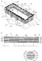
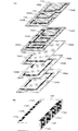
次に、図7及び図8を参照しながら、本発明の実施例7を説明する。図7(A)は、本実施例の可変インダクタの積層体の分解斜視図,図7(B)は前記積層体の外観斜視図である。図8は、本実施例の可変インダクタの回路構成を示す図である。図8に示すように、本実施例の可変インダクタ150は、積層体152内で、一つのメインインダクタ154の上に、3つの制御インダクタ160,164,168が対向配置されており、各制御インダクタに、スイッチ176,177,178が接続された構成となっている。前記制御インダクタ160,164,168は、互いに重なることがないように配置されている。
Next, Embodiment 7 of the present invention will be described with reference to FIGS. FIG. 7A is an exploded perspective view of the multilayer body of the variable inductor of this embodiment, and FIG. 7B is an external perspective view of the multilayer body. FIG. 8 is a diagram illustrating a circuit configuration of the variable inductor according to the present embodiment. As shown in FIG. 8, the
前記積層体152は、図7(A)に示すように、絶縁層156A〜156Eを積層したものである。絶縁層156A〜156Cの表面には、導体パターン154A〜154Cが形成されており、絶縁層156Bに設けられたスルーホール158Bと、絶縁層156Cに設けられたスルーホール158Cを介して、前記導体パターン154A〜154Cが接続され、メインインダクタ154を構成している。また、絶縁層156Dには、導体パターン160A,164A,168Aが形成されており、絶縁層156Eには、導体パターン160B,164B,168Bとともにスルーホール162,166,170が形成されている。
As shown in FIG. 7A, the
そして、前記導体パターン160Aと160Bがスルーホール162で接続されて制御インダクタ160を構成する。同様に、導体パターン164Aと164Bがスルーホール166で接続されて制御インダクタ164を構成し、導体パターン168Aと168Bがスルーホール170で接続されて制御インダクタ168を構成している。また、前記絶縁層156Aの下面や、絶縁層156Eの上面には、図示しない他の絶縁層が積層される。なお、絶縁層156A〜156Eとしては、例えば、Ni−Zn−Cu系フェライト、アルミナセラミックス、MgO−CaO−SiO2系誘電体セラミックスなどが用いられる。
The
以上のようにして構成された積層体152の表面には、端子電極172A〜172Hが設けられ、メインインダクタ154の両端は、端子電極172A及び172Eに接続される。制御インダクタ160の両端は、端子電極174B及び172Fに接続され、制御インダクタ164の両端は、端子電極172C及び172Gに接続され、制御インダクタ168の両端は、端子電極172D及び172Hに接続される。前記端子電極172B及び172F間には、図8に示すスイッチ176が接続され、端子電極172C及び172G間には、スイッチ177が接続され、端子電極172D及び172H間には、スイッチ178が接続される。
このような構成の可変インダクタ150では、3つのスイッチ176,177,178のON/OFFの組み合わせにより、8段階の切り替えが可能となっている。また、図示の例では、3つの制御インダクタを設けているが、結合の異なる複数の制御インダクタを設け、それを切り替えることにより、複数の値の可変インダクタとすることができる。n個の制御インダクタを利用すると仮定した場合、メインインダクタと複数の制御インダクタのそれぞれとの間の結合係数の比を、およそ2の階乗(1:2:4:8・・・2n)となるようにすると、nビットの可変インダクタを実現することができる。他の作用・効果は、上述した実施例1と同様である。
The
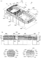
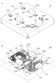
次に、図9を参照しながら、本発明の実施例8について説明する。図9(A)は本実施例の外観斜視図,図9(B)はインダクタ配置を示す斜視図である。本実施例の可変インダクタ180の積層体182の内側のインダクタ配置は、上述した実施例5と同様となっている。すなわち、3つの巻回軸に沿ってそれぞれ巻回したインダクタ部94,96,98からなるメインインダクタ92と、これらインダクタ部94,96,98と導体パターンが交互になるように積層された制御インダクタ100,106,110を備えている。本実施例では、積層体182の側面ではなく、上面に8つの端子電極184A〜184Hが設けられている。そして、端子電極184Bと184Cの間にスイッチ116Aが接続され、端子電極184Fと184Gの間にスイッチ116Bが接続されている。また、スイッチ116Cは、前記端子電極184D及び184Hに接続された引出部186A及び186Bの間に接続されている。
Next, Embodiment 8 of the present invention will be described with reference to FIG. FIG. 9A is an external perspective view of this embodiment, and FIG. 9B is a perspective view showing an inductor arrangement. The inductor arrangement inside the
このほか、前記端子電極184Cと導体パターン100Gの端部との間には、コンデンサ188Aが設けられている。同様に、端子電極184Fと導体パターン106Fの端部の間にはコンデンサ188Bが設けられ、端子電極184Hと導体パターン110Fの間にはコンデンサ188Cが設けられている。すなわち、本実施例では、コンデンサ188A〜188Cが、積層体182の内側に内蔵された構成となっている。従って、本実施例の可変インダクタ180の外観を見ると、図9(A)に示すように、積層体182の表面には、端子電極184A〜184H,引出部186A及び186B,スイッチ116A〜116Cのみが見えるようになっている。本実施例の基本的効果は、上述した実施例5と同様であるが、コンデンサを内蔵させることができるため、周辺回路を小型化するとともに、スイッチング回路の部品点数を削減できるという効果も得られる。
In addition, a
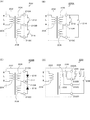
次に、図10を参照しながら、本発明の実施例9について説明する。図10は、本実施例の回路構成を示す図である。まず、図10(A)に示す可変インダクタ200は、積層体202の内側に、メインインダクタ204と、それに対向する2つの制御インダクタ206及び208が設けられた構成となっている。そして、制御インダクタ206は、端部が端子電極210A及び210Bに接続され、他方の制御インダクタ208は、端部が端子電極210B及び210Cに接続されている。すなわち、制御インダクタ206及び208は、それぞれ一方の端部が、共通の端子電極210Bに接続された構成となっている。そして、端子電極210A及び210B間にはスイッチ212が接続され、端子電極210B及び210C間には、スイッチ214が接続されている。
Next, Embodiment 9 of the present invention will be described with reference to FIG. FIG. 10 is a diagram showing a circuit configuration of the present embodiment. First, the
次に、図10(B)に示す可変インダクタ200Aは、制御インダクタ206及び208と端子電極との接続は、前記図10(A)に示した例と同様であるが、スイッチの接続構成が異なっており、スイッチ214は、端子電極210Aと210C間に接続されている。更に、図10(C)に示す可変インダクタ200Bは、前記図10(A)に示す例と同様の接続形態であるが、スイッチ212及び214の代わりに、PINダイオード216が端子電極210A及び210B間に、また、PINダイオード218が端子電極210B及び210C間に、カップリングコンデンサ217を介してそれぞれ接続されている。
Next, in the
また、図10(D)に示す可変インダクタ220は、積層体222の内側に、メインインダクタ224と、それに対向する3つの制御インダクタ226,228,230が設けられた構成となっている。これら制御インダクタ226〜230は、積層体222の積層方向(図示の例では左右方向)に重ねて配置されている。そして、制御インダクタ226は、端部が端子電極232A及び232Bに接続され、制御インダクタ228は、端部が端子電極232A及び232Cに接続され、制御インダクタ230は、端部が端子電極232A及び232Dに接続されている。すなわち、制御インダクタ226〜230は、それぞれ一方の端部が、共通の端子電極232Aに接続された構成となっている。そして、端子電極232A及び232B間には、スイッチ234が接続され、端子電極232A及び232C間には、スイッチ236が接続され、端子電極232A及び232D間には、スイッチ238が接続されている。このように、共通の端子電極を用いることにより、上述した実施例の効果に加えて、端子数を大幅に削減できるので、可変インダクタ220を小型化できるという効果が得られる。
In addition, the
次に、図11を参照しながら本発明の実施例11を説明する。図11(A)はインダクタ配置を示す斜視図,図11(B)は前記(A)を矢印F11方向から見た側面図,図11(C)は等価回路,図11(D)はスイッチを含む回路である。上述した実施例9は、複数の制御インダクタのそれぞれ一つの端部が、共通の端子電極を利用した例であるが、本実施例は、メインインダクタと制御インダクタが、共通の端子電極に接続される例である。図11に示すように、可変インダクタ250は、積層体252とスイッチ264を備えている。前記積層体252内には、メインインダクタ254と制御インダクタ258が隣接して対向配置された構成となっている。また、積層体252の表面には、前記メインインダクタ254及び258の端部が接続される端子電極262A〜262Fが適宜位置に形成されている。
Next, Embodiment 11 of the present invention will be described with reference to FIG. 11 (A) is a perspective view showing the inductor arrangement, FIG. 11 (B) is a side view of FIG. 11 (A) viewed from the direction of arrow F11, FIG. 11 (C) is an equivalent circuit, and FIG. 11 (D) is a switch. It is a circuit including. Embodiment 9 described above is an example in which one end of each of the plurality of control inductors uses a common terminal electrode, but in this embodiment, the main inductor and the control inductor are connected to the common terminal electrode. This is an example. As illustrated in FIG. 11, the
前記メインインダクタ254は、複数の導体パターン254A〜254Eが、積層体252の積層方向に沿って巻回するように積層されており、これら導体パターン254A〜254Eは、スルーホール256A〜256Dによって接続されている。そして、一方の端部(導体パターン254A側)は、積層体252の表面の端子電極262Aに接続され、他方の端部(導体パターン254E側)は、端子電極262Dに接続されている。同様に、制御インダクタ258も、複数の導体パターン258A〜258Eが積層方向に沿って巻回するように積層されており、これら導体パターン258A〜258Eは、スルーホール260B〜260Eによって接続されている。また、前記導体パターン258Aは、スルーホール260Aによって、前記メインインダクタ254の導体パターン254Eに接続されている。そして、制御インダクタ258の一方の端部(導体パターン258E側)は端子電極262Fに接続され、他方の端部はメインインダクタ254の導体パターン254Eを介して端子電極262Dに接続される。更に、これら端子電極262D及び262Fの間には、積層体252の外部で、スイッチ264が接続されている。本実施例のように、メインインダクタと制御インダクタの端部を共通の端子電極に接続するようにしても、上述した実施例1と同様の効果が得られる。
The
なお、本発明は、上述した実施例に限定されるものではなく、本発明の要旨を逸脱しない範囲内において種々変更を加え得ることができる。例えば、以下のものも含まれる。
(1)前記実施例に示した材料,寸法は一例であり、必要に応じて適宜変更してよい。
(2)前記実施例に示した導体パターン,端子電極の形状は一例であり、同様の効果を奏するように適宜変更可能である。
(3)メインインダクタに対向配置する制御インダクタの数や、巻回軸の数も一例であり、必要に応じて適宜増減してよい。また、メインインダクタに対向するようであれば、制御インダクタの配置も適宜変更可能である。
(4)メインインダクタや制御インダクタのターン数も一例であり、必要に応じて適宜変更してよい。例えば、制御インダクタは、3/4ターン程度であっても、上述した実施例と同様の効果が得られる。
(5)本発明の可変インダクタは、例えば、アンテナ装置などが好適な利用例であるが、他の公知の各種の電子機器に適用可能である。
In addition, this invention is not limited to the Example mentioned above, A various change can be added in the range which does not deviate from the summary of this invention. For example, the following are also included.
(1) The materials and dimensions shown in the above embodiments are examples, and may be appropriately changed as necessary.
(2) The shape of the conductor pattern and the terminal electrode shown in the above embodiment is an example, and can be appropriately changed so as to achieve the same effect.
(3) The number of control inductors arranged opposite to the main inductor and the number of winding shafts are examples, and may be appropriately increased or decreased as necessary. In addition, the arrangement of the control inductor can be appropriately changed as long as it faces the main inductor.
(4) The number of turns of the main inductor and the control inductor is also an example, and may be changed as needed. For example, even if the control inductor has about 3/4 turns, the same effect as the above-described embodiment can be obtained.
(5) The variable inductor of the present invention is preferably used in, for example, an antenna device, but can be applied to various other known electronic devices.
本発明によれば、積層体内部に積層方向に沿って巻回された主コイル導体に対して、調整用コイル導体を積層体内で対向配置し、各コイル導体の端部を積層体表面の端子電極に接続するとともに、前記調整用コイル導体端部に接続する一対の端子電極間に、積層体外部でスイッチ素子を接続することとした。このため、可変インダクタの用途に適用できる。特に、アンテナ装置などに用いられる可変インダクタの用途に好適である。 According to the present invention, the adjustment coil conductor is disposed opposite to the main coil conductor wound in the laminate in the lamination direction in the laminate, and the end of each coil conductor is connected to the terminal on the laminate surface. In addition to being connected to the electrodes, a switch element was connected outside the laminate between a pair of terminal electrodes connected to the adjustment coil conductor end. For this reason, it is applicable to the use of a variable inductor. In particular, it is suitable for use as a variable inductor used in an antenna device or the like.
10:可変インダクタ
12:積層体
14:メインインダクタ(主コイル)
14A〜14G,18A〜18G:導体パターン
15A〜15F,19A〜19F:スルーホール
16A,16B,20A,20B:端部
18:制御インダクタ(調整用コイル)
22A〜22F:端子電極
24:シールド層
26:スイッチ
30:可変インダクタ
32:積層体
40:可変インダクタ
42:積層体
44:メインインダクタ
44A〜44F,48A,48B,54A〜54D,62A:導体パターン
46A〜46E,50,56A〜56C:スルーホール
48,54,62:制御インダクタ
60A〜60H:端子電極
64A,64B,64C:スイッチ
70:可変インダクタ
72:積層体
74:メインインダクタ
74A〜74E,80A〜80E,84A〜84F:導体パターン
76A〜76D,82A〜82D,86A〜86E:スルーホール
80,84:制御インダクタ
88A〜88H:端子電極
89A,89B:スイッチ
90:可変インダクタ
91:積層体
92:メインインダクタ
94,96,98:インダクタ部
94A〜94E,96A〜96E,98A〜98F,100A〜100F,106A〜106F,110A〜110F:導体パターン
95A〜95D,97A〜97D,99A〜99E,102A〜102F,108A〜108E,112A〜112E:スルーホール
100,106,110:制御インダクタ
114A〜114H:端子電極
116A〜116C:スイッチ
120:可変インダクタ
121:積層体
122:メインインダクタ
124,128:インダクタ部
124A〜124E,128A〜128E,132A〜132E,136A〜136E:導体パターン
126A〜126D,130A〜130D,134A〜134E,138A〜138E:スルーホール
132,136:制御インダクタ
140A〜140H:端子電極
142A,142B:スイッチ
150:可変インダクタ
152:積層体
154:メインインダクタ
154A〜154C,160A,160B,164A,164B,168A,168B:導体パターン
156A〜156E:絶縁層
158B,162,166,170:スルーホール
160,164,168:制御インダクタ
172A〜172H:端子電極
176,177,178:スイッチ
180:可変インダクタ
182:積層体
184A〜184H:端子電極
186A,186B:引出部
188A〜188C:コンデンサ
200,200A,200B:可変インダクタ
202:積層体
204:メインインダクタ
206,208:制御インダクタ
210A〜210C:端子電極
212,214:スイッチ
216,218:PINダイオード
217:カップリングコンデンサ
220:可変インダクタ
222:積層体
224:メインインダクタ
226,228,230:制御インダクタ
232A〜232D:端子電極
234,236,238:スイッチ
250:可変インダクタ
252:積層体
254:メインインダクタ
254A〜254E,258A〜258E:導体パターン
256A〜256D,260A〜260E:スルーホール
258:制御インダクタ
262A〜262F:端子電極
264:スイッチ
10: Variable inductor 12: Laminated body 14: Main inductor (main coil)
14A-14G, 18A-18G:
22A-22F: Terminal electrode 24: Shield layer 26: Switch 30: Variable inductor 32: Laminate body 40: Variable inductor 42: Laminate body 44: Main inductor 44A-44F, 48A, 48B, 54A-54D, 62A: Conductor pattern 46A ˜46E, 50, 56A to 56C: Through hole 48, 54, 62: Control inductor 60A-60H: Terminal electrode 64A, 64B, 64C: Switch 70: Variable inductor 72: Multilayer 74: Main inductor 74A-74E, 80A 80E, 84A to 84F: Conductor pattern 76A to 76D, 82A to 82D, 86A to 86E: Through hole 80, 84: Control inductor 88A to 88H: Terminal electrode 89A, 89B: Switch 90: Variable inductor 91: Multilayer body 92: Main Inductor 9 , 96, 98: Inductor portions 94A to 94E, 96A to 96E, 98A to 98F, 100A to 100F, 106A to 106F, 110A to 110F: Conductor patterns 95A to 95D, 97A to 97D, 99A to 99E, 102A to 102F, 108A To 108E, 112A to 112E: through holes 100, 106, 110: control inductors 114A to 114H: terminal electrodes 116A to 116C: switch 120: variable inductor 121: laminated body 122: main inductor 124, 128: inductor sections 124A to 124E, 128A to 128E, 132A to 132E, 136A to 136E: Conductor patterns 126A to 126D, 130A to 130D, 134A to 134E, 138A to 138E: Through holes 132, 136: Control inductor 1 40A to 140H: Terminal electrodes 142A and 142B: Switch 150: Variable inductor 152: Stacked body 154: Main inductors 154A to 154C, 160A, 160B, 164A, 164B, 168A, 168B: Conductive patterns 156A to 156E: Insulating layers 158B, 162 , 166, 170: Through holes 160, 164, 168: Control inductors 172A to 172H: Terminal electrodes 176, 177, 178: Switch 180: Variable inductor 182: Laminates 184A to 184H: Terminal electrodes 186A, 186B: Lead portions 188A to 188A 188C: Capacitors 200, 200A, 200B: Variable inductor 202: Laminated body 204: Main inductors 206, 208: Control inductors 210A to 210C: Terminal electrodes 212, 214: Switch 216 18: PIN diode 217: coupling capacitor 220: variable inductor 222: laminated body 224: main inductors 226, 228, 230: control inductors 232A to 232D: terminal electrodes 234, 236, 238: switch 250: variable inductor 252: laminated body 254: Main inductors 254A to 254E, 258A to 258E: Conductor patterns 256A to 256D, 260A to 260E: Through holes 258: Control inductors 262A to 262F: Terminal electrodes 264: Switches
Claims (15)
該主コイル導体と対向するように前記積層体の内部に配置された調整用コイル導体と、
前記積層体表面に設けられており、前記各コイル導体の端部が接続される端子電極と、
前記調整用コイル導体の端部が接続された一対の端子電極間に、前記積層体の外部で接続されたスイッチ素子と、
を備えたことを特徴とする可変インダクタ。 A main coil conductor wound along the stacking direction inside the stack,
An adjustment coil conductor disposed inside the laminate so as to face the main coil conductor;
A terminal electrode provided on the surface of the laminate, to which an end of each coil conductor is connected;
Between the pair of terminal electrodes to which the ends of the adjustment coil conductor are connected, a switch element connected outside the laminate,
A variable inductor characterized by comprising:
An antenna device, wherein the variable inductor according to claim 1 is used in a matching circuit.
Priority Applications (1)
| Application Number | Priority Date | Filing Date | Title |
|---|---|---|---|
| JP2005317646A JP2007123785A (en) | 2005-10-31 | 2005-10-31 | Variable inductor and antenna device using it |
Applications Claiming Priority (1)
| Application Number | Priority Date | Filing Date | Title |
|---|---|---|---|
| JP2005317646A JP2007123785A (en) | 2005-10-31 | 2005-10-31 | Variable inductor and antenna device using it |
Publications (1)
| Publication Number | Publication Date |
|---|---|
| JP2007123785A true JP2007123785A (en) | 2007-05-17 |
Family
ID=38147255
Family Applications (1)
| Application Number | Title | Priority Date | Filing Date |
|---|---|---|---|
| JP2005317646A Pending JP2007123785A (en) | 2005-10-31 | 2005-10-31 | Variable inductor and antenna device using it |
Country Status (1)
| Country | Link |
|---|---|
| JP (1) | JP2007123785A (en) |
Cited By (2)
| Publication number | Priority date | Publication date | Assignee | Title |
|---|---|---|---|---|
| JP2013504885A (en) * | 2009-09-17 | 2013-02-07 | ローベルト ボツシユ ゲゼルシヤフト ミツト ベシユレンクテル ハフツング | Integrated circuits for information transmission |
| WO2023136922A1 (en) * | 2022-01-13 | 2023-07-20 | Qualcomm Incorporated | Package comprising substrate with coupling element for integrated devices |
Citations (11)
| Publication number | Priority date | Publication date | Assignee | Title |
|---|---|---|---|---|
| JPS6221517U (en) * | 1985-07-24 | 1987-02-09 | ||
| JPH0281410A (en) * | 1988-09-17 | 1990-03-22 | Toko Inc | Current controlled multilayer inductor |
| JPH0287508A (en) * | 1988-09-22 | 1990-03-28 | Toko Inc | laminated transformer |
| JPH07192922A (en) * | 1993-12-27 | 1995-07-28 | Taiyo Yuden Co Ltd | Layered inductance element and adjusting method of inductance |
| JPH0935942A (en) * | 1995-07-20 | 1997-02-07 | Kokusai Electric Co Ltd | Step variable inductor |
| JPH11329850A (en) * | 1998-05-18 | 1999-11-30 | Mitsubishi Materials Corp | Laminated chip component and method of using same |
| JP2001210520A (en) * | 2000-01-27 | 2001-08-03 | Tdk Corp | Laminated composite, component |
| JP2002151953A (en) * | 2000-11-08 | 2002-05-24 | Matsushita Electric Ind Co Ltd | Frequency switching device for voltage controlled oscillator |
| JP2002280222A (en) * | 2001-03-19 | 2002-09-27 | Internatl Business Mach Corp <Ibm> | Integrated variable inductor, inductor/varactor tuning circuit |
| JP2003068571A (en) * | 2001-08-27 | 2003-03-07 | Nec Corp | Variable capacitor and variable inductor and high-frequency circuit module provided with them |
| WO2005034239A2 (en) * | 2003-09-25 | 2005-04-14 | Qualcomm Incorporated | Variable inductor for integrated circuit and printed circuit board |
-
2005
- 2005-10-31 JP JP2005317646A patent/JP2007123785A/en active Pending
Patent Citations (12)
| Publication number | Priority date | Publication date | Assignee | Title |
|---|---|---|---|---|
| JPS6221517U (en) * | 1985-07-24 | 1987-02-09 | ||
| JPH0281410A (en) * | 1988-09-17 | 1990-03-22 | Toko Inc | Current controlled multilayer inductor |
| JPH0287508A (en) * | 1988-09-22 | 1990-03-28 | Toko Inc | laminated transformer |
| JPH07192922A (en) * | 1993-12-27 | 1995-07-28 | Taiyo Yuden Co Ltd | Layered inductance element and adjusting method of inductance |
| JPH0935942A (en) * | 1995-07-20 | 1997-02-07 | Kokusai Electric Co Ltd | Step variable inductor |
| JPH11329850A (en) * | 1998-05-18 | 1999-11-30 | Mitsubishi Materials Corp | Laminated chip component and method of using same |
| JP2001210520A (en) * | 2000-01-27 | 2001-08-03 | Tdk Corp | Laminated composite, component |
| JP2002151953A (en) * | 2000-11-08 | 2002-05-24 | Matsushita Electric Ind Co Ltd | Frequency switching device for voltage controlled oscillator |
| JP2002280222A (en) * | 2001-03-19 | 2002-09-27 | Internatl Business Mach Corp <Ibm> | Integrated variable inductor, inductor/varactor tuning circuit |
| JP2003068571A (en) * | 2001-08-27 | 2003-03-07 | Nec Corp | Variable capacitor and variable inductor and high-frequency circuit module provided with them |
| WO2005034239A2 (en) * | 2003-09-25 | 2005-04-14 | Qualcomm Incorporated | Variable inductor for integrated circuit and printed circuit board |
| JP2007507106A (en) * | 2003-09-25 | 2007-03-22 | クゥアルコム・インコーポレイテッド | Variable inductors for integrated circuits and printed wiring boards |
Cited By (3)
| Publication number | Priority date | Publication date | Assignee | Title |
|---|---|---|---|---|
| JP2013504885A (en) * | 2009-09-17 | 2013-02-07 | ローベルト ボツシユ ゲゼルシヤフト ミツト ベシユレンクテル ハフツング | Integrated circuits for information transmission |
| WO2023136922A1 (en) * | 2022-01-13 | 2023-07-20 | Qualcomm Incorporated | Package comprising substrate with coupling element for integrated devices |
| US12027476B2 (en) | 2022-01-13 | 2024-07-02 | Qualcomm Incorporated | Package comprising substrate with coupling element for integrated devices |
Similar Documents
| Publication | Publication Date | Title |
|---|---|---|
| JP5915778B2 (en) | LC composite parts | |
| JP4535131B2 (en) | Multilayer coil parts | |
| KR100466976B1 (en) | Multilayer inductor | |
| JP5621946B2 (en) | Multilayer inductor and power circuit module | |
| KR101843283B1 (en) | Coil Electronic Component | |
| JP6566455B2 (en) | Coil component and manufacturing method thereof | |
| KR102632343B1 (en) | Inductor array component and board for mounting the same | |
| KR20160032581A (en) | Inductor array chip and board for mounting the same | |
| KR102385508B1 (en) | Common mode noise filter | |
| US12119162B2 (en) | Coil component | |
| JP2014022723A (en) | Chip element, multi-layered chip element and method of producing the same | |
| WO2017179590A1 (en) | Passive element array and printed wiring board | |
| JP2000133521A (en) | Laminated coil | |
| US20160042860A1 (en) | Inductor | |
| KR101153496B1 (en) | A layered inductor and a manufacturing method thereof | |
| JP2007123785A (en) | Variable inductor and antenna device using it | |
| KR102064075B1 (en) | High frequency inductor | |
| US12112873B2 (en) | Coil component | |
| KR20200107151A (en) | Coil component | |
| KR101862465B1 (en) | Coil component | |
| JP6658234B2 (en) | Multilayer electronic components | |
| CN112038041B (en) | Laminated coil component | |
| KR20200004157A (en) | Inductor | |
| JP6962104B2 (en) | Coil parts and their manufacturing methods | |
| JP6288386B2 (en) | Surface mount LC device |
Legal Events
| Date | Code | Title | Description |
|---|---|---|---|
| A621 | Written request for application examination |
Free format text: JAPANESE INTERMEDIATE CODE: A621 Effective date: 20080426 |
|
| A977 | Report on retrieval |
Free format text: JAPANESE INTERMEDIATE CODE: A971007 Effective date: 20100906 |
|
| A131 | Notification of reasons for refusal |
Free format text: JAPANESE INTERMEDIATE CODE: A131 Effective date: 20100914 |
|
| A02 | Decision of refusal |
Free format text: JAPANESE INTERMEDIATE CODE: A02 Effective date: 20110201 |