JP2007103669A - Short pulse light source - Google Patents
Short pulse light source Download PDFInfo
- Publication number
- JP2007103669A JP2007103669A JP2005291468A JP2005291468A JP2007103669A JP 2007103669 A JP2007103669 A JP 2007103669A JP 2005291468 A JP2005291468 A JP 2005291468A JP 2005291468 A JP2005291468 A JP 2005291468A JP 2007103669 A JP2007103669 A JP 2007103669A
- Authority
- JP
- Japan
- Prior art keywords
- region
- semiconductor laser
- optical pulse
- light source
- short pulse
- Prior art date
- Legal status (The legal status is an assumption and is not a legal conclusion. Google has not performed a legal analysis and makes no representation as to the accuracy of the status listed.)
- Withdrawn
Links
Images


Landscapes
- Semiconductor Lasers (AREA)
Abstract
Description
本発明は、超高速な短パルス光を発生する半導体レーザによる短パルス光源に関する。 The present invention relates to a short pulse light source using a semiconductor laser that generates ultrafast short pulse light.
半導体レーザによる超高速な短パルス光源として、パルス光を生成する可飽和吸収領域をモノリシックに集積した受動モード同期半導体レーザがある。この半導体レーザは、活性領域で発生した光がレーザ共振器内を周回する際に、可飽和吸収領域の非線形吸収特性により急峻なパルスとして成長し、短パルス光が得られる。 As an ultrafast short pulse light source using a semiconductor laser, there is a passive mode-locked semiconductor laser in which a saturable absorption region for generating pulsed light is monolithically integrated. This semiconductor laser grows as a steep pulse due to the nonlinear absorption characteristics of the saturable absorption region when light generated in the active region circulates in the laser resonator, and a short pulse light is obtained.
図6は、従来の受動モード同期半導体レーザの構成例を示す(非特許文献1)。図において、受動モード同期半導体レーザは、レーザ共振器端面61に接した可飽和吸収領域63、光導波路領域64、他方のレーザ共振器端面62に接した活性領域65で構成される。可飽和吸収領域63と光導波路領域64との間、光導波路領域64と活性領域65との間には、それぞれ電極分離溝66,67が設けられる。活性領域65に直流電流、可飽和吸収領域63に逆バイアス電圧を印加することにより、活性層68でモード同期によるパルス光を発生させることができる。
FIG. 6 shows a configuration example of a conventional passive mode-locked semiconductor laser (Non-Patent Document 1). In the figure, the passive mode-locked semiconductor laser includes a saturable absorption region 63 in contact with the laser
図7は、従来の受動モード同期半導体レーザの他の構成例を示す(特許文献1)。ここに示す半導体レーザは、衝突パルスモード同期(Colliding-pulse mode-locked 、以下「CPM」という)半導体レーザと呼ばれる。CPM半導体レーザは、レーザ共振器の中央に可飽和吸収領域71を設け、その両側に活性領域72,73を配置した構成である。このような構造により、レーザ共振器内を逆方向に周回する2つのパルス光が同時に可飽和吸収領域71に到達し、効率的に短パルス光を発生させることが可能となる。なお、一般的には、先に示した従来の受動モード同期半導体レーザの構成例(非特許文献1)と同様に、可飽和吸収領域71と活性領域72,73との間には、それぞれ電極分離溝が設けられる(図7に図示せず)。
FIG. 7 shows another configuration example of a conventional passive mode-locked semiconductor laser (Patent Document 1). The semiconductor laser shown here is called a colliding-pulse mode-locked (hereinafter referred to as “CPM”) semiconductor laser. The CPM semiconductor laser has a configuration in which a
CPM半導体レーザから発生されるパルス光の繰り返し周期は次のように求められる。図7において、レーザ共振器長(素子長)をL、導波路の実効屈折率をnとする。レーザ共振器内には2つのパルス光が存在するため、パルス光の時間間隔はレーザ共振器の周回時間τの1/2となる。したがって、パルス光の繰り返し周期Tは、
T=1/(τ/2)=c/nL (cは光速) …(1)
と与えられる。非特許文献2のCPM半導体レーザは、レーザ共振器長L= 250μmとすることにより、繰り返し周期T= 350GHzのパルス光を得ている。
T = 1 / (τ / 2) = c / nL (c is the speed of light) (1)
And given. The CPM semiconductor laser of Non-Patent
繰り返し周期がサブテラヘルツを超えるような例えばテラヘルツ級の超高速パルス光を得るためには、式(1) から分かるように、レーザ共振器長Lを短くする必要がある。例えば、繰り返し周期T=1THzのパルス光を発生させるには、導波路の実効屈折率n=3.5 とすると、レーザ共振器長をL=86μmとしなければならない。図7において、可飽和吸収領域71の長さを非特許文献2と同じ50μmと仮定すると、活性領域72,73の長さは合計で36μmしかとることができない。そのために十分な利得が得られず、高出力のパルス光を安定して発生させることが困難であった。
In order to obtain, for example, terahertz-class ultrafast pulsed light whose repetition period exceeds sub-terahertz, it is necessary to shorten the laser resonator length L as can be seen from equation (1). For example, in order to generate pulsed light with a repetition period T = 1 THz, if the effective refractive index n of the waveguide is 3.5, the laser resonator length must be L = 86 μm. In FIG. 7, assuming that the length of the
本発明は、安定して高出力な超高速パルス光を発生させることができる半導体レーザによる短パルス光源を提供することを目的とする。 It is an object of the present invention to provide a short pulse light source using a semiconductor laser that can generate ultrahigh-speed pulsed light with high output stably.
本発明の短パルス光源は、第1および第2の半導体レーザ共振器端面で構成されたファブリ・ペロー型の半導体レーザ共振器内に、1つの利得領域と、2以上の光パルス形成領域が半導体レーザ共振器の光波伝搬軸上に直列に配置され、2以上の光パルス形成領域のそれぞれは、半導体レーザ共振器の光波伝搬軸上に、第1の活性領域、可飽和吸収領域、第2の活性領域の順に配置され、かつ可飽和吸収領域が光パルス形成領域の中央に配置され、衝突パルスモード同期によって短パルス光を生成する構成であり、利得領域は、1つの光パルス形成領域の長さの正数倍とする。 The short pulse light source of the present invention includes one gain region and two or more optical pulse forming regions in a Fabry-Perot type semiconductor laser resonator composed of first and second semiconductor laser resonator end faces. The two or more optical pulse forming regions are arranged in series on the light wave propagation axis of the laser resonator, and each of the two or more optical pulse forming regions has a first active region, a saturable absorption region, a second absorption region on the light wave propagation axis of the semiconductor laser resonator. The active region is arranged in order, the saturable absorption region is arranged in the center of the optical pulse forming region, and the short pulse light is generated by the collision pulse mode synchronization. The gain region is the length of one optical pulse forming region. It is a positive multiple of.
ここで、2以上の光パルス形成領域は、利得領域の両側に配置された構成としてもよい。このとき、利得領域の両側に配置される光パルス形成領域は、それぞれ少なくとも1つあり、かつ同数としてもよい。また、利得領域の両側に配置される光パルス形成領域は、それぞれ少なくとも1つあり、かつ異なる数としてもよい。 Here, two or more optical pulse forming regions may be arranged on both sides of the gain region. At this time, there are at least one optical pulse forming region arranged on both sides of the gain region, and the number may be the same. Further, there are at least one optical pulse forming region arranged on both sides of the gain region, and the number may be different.
また、2以上の光パルス形成領域は、利得領域の片側に配置された構成としてもよい。 Two or more optical pulse forming regions may be arranged on one side of the gain region.
本発明は、2以上の光パルス形成領域と、光パルス形成領域の長さの正数倍の利得領域をモノリシックに集積化した構成であるので、効率よく短パルス光を発生させ、安定かつ高出力の超高速パルス光を生成することができる。 The present invention has a structure in which two or more optical pulse forming regions and a gain region that is a positive multiple of the length of the optical pulse forming region are monolithically integrated. It is possible to generate output ultrafast pulsed light.
(第1の実施形態)
図1は、本発明の短パルス光源の第1の実施形態を示す。
図において、本実施形態の短パルス光源は、化合物半導体を材料とする半導体レーザであり、第1の共振器端面11と第2の共振器端面12とにより、ファブリ・ペロー型の半導体レーザ共振器を構成している。各共振器端面は、通常の半導体レーザと同様に劈開により形成してもよいし、半導体プロセスのエッチングにより得られる「エッチドミラー」であってもよい。さらには、これらの端面に誘電体多層膜を蒸着したものであってもよい。
(First embodiment)
FIG. 1 shows a first embodiment of the short pulse light source of the present invention.
In the figure, the short pulse light source of the present embodiment is a semiconductor laser made of a compound semiconductor, and a Fabry-Perot type semiconductor laser resonator is formed by a first
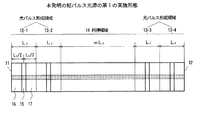
本実施形態における半導体レーザ共振器は、第1の共振器端面11から第2の共振器端面12へ向けて、順に2つの光パルス形成領域13−1,13−2、利得領域14、2つの光パルス形成領域13−3,13−4の各領域が配置された構成になっている。
The semiconductor laser resonator according to the present embodiment includes two optical pulse forming regions 13-1 and 13-2, a gain region 14, two components in order from the first
各光パルス形成領域は、その中央に可飽和吸収領域15を設け、その両側に活性領域16,17を配置した構成であり、図7に示すCPM半導体レーザの構成と同じになっている。利得領域14の長さは、各光パルス形成領域13の長さの正数倍とする。図1では、1つの光パルス形成領域13の長さをL0 、利得領域14の長さをmL0 と表している(mは正数)。
Each optical pulse forming region has a configuration in which a
なお、利得領域14と、各光パルス形成領域13を構成する活性領域16,17は、半導体レーザ共振器を導波する光に対して増幅可能な領域であり、機能的にも物理構成としても同様のものであるが、説明を容易にするために異なる名称を用いている。したがって、隣接する光パルス形成領域13の活性領域16,17については、電気的に分離する必要はない。同様に、隣接する利得領域14と光パルス形成領域13の活性領域16,17についても、電気的に分離する必要はない(図1では点線で表示)。
The gain region 14 and the
一方、光パルス形成領域13を構成する活性領域16,17と可飽和吸収領域15は、通常のCPM半導体レーザと同様に電気的に分離する必要がある。そのために、これらの領域との間に電極分離溝を配置してもよい(図1では実線で表示)。
On the other hand, the
本実施形態の利得領域14と、各光パルス形成領域13を構成する活性領域16,17に、レーザ発振閾値を超える直流電流を印加し、かつ可飽和吸収領域15に逆バイアス電圧を印加することにより、半導体レーザは受動モード同期により短パルス光を発生する。発生する短パルス光の特性について、図2を参照して説明する。
A direct current exceeding the laser oscillation threshold is applied to the gain region 14 and the
図2は、第1の実施形態における半導体レーザ共振器内のパルス光の動作を示す。光パルス形成領域13−1,13−2,13−3,13−4では、CPM半導体レーザを直列に接続した高調波CPM半導体レーザと同様の動作になる。すなわち、各光パルス形成領域では、それぞれ2個のパルス光が周回しており、4つの光パルス形成領域では合計8個のパルス光が周回し、可飽和吸収領域15で逆方向に周回するパルス光が衝突する。この衝突により、効率的に短パルス光を生成することができる。本発明の短パルス光源から発生するパルス光の繰り返し周期Tは、基本的なCPM半導体レーザと同様に式(1) で与えられ、
T=c/nL0 …(2)
となる。
FIG. 2 shows the operation of pulsed light in the semiconductor laser resonator according to the first embodiment. In the optical pulse forming regions 13-1, 13-2, 13-3, and 13-4, the operation is the same as that of the harmonic CPM semiconductor laser in which the CPM semiconductor lasers are connected in series. That is, two pulse lights circulate in each optical pulse formation region, a total of eight pulse lights circulate in the four optical pulse formation regions, and pulses that circulate in the reverse direction in the
T = c / nL 0 (2)
It becomes.
一方、利得領域14内では、2m個の光パルスが周回しており(図2の例ではm=3)、増幅作用によりパルス光のパワーが増幅される。繰り返し周期の高速化を図ると、各光パルス形成領域13の活性領域が短くなるが、利得領域14の長さを決める定数mは、パルス光の繰り返し周期と無関係に設定できる値であるので、mを大きくすることにより(利得領域14を長くすることにより)十分な利得が得られ、高出力のパルス光を安定して発生させることができる。 On the other hand, 2m optical pulses circulate in the gain region 14 (m = 3 in the example of FIG. 2), and the power of the pulsed light is amplified by the amplification action. When the repetition cycle is increased in speed, the active region of each optical pulse forming region 13 is shortened, but the constant m that determines the length of the gain region 14 is a value that can be set regardless of the repetition cycle of the pulsed light. By increasing m (by increasing the gain region 14), a sufficient gain can be obtained, and high-power pulsed light can be stably generated.
(第2の実施形態)
図3は、本発明の短パルス光源の第2の実施形態を示す。
本実施形態における半導体レーザ共振器は、第1の共振器端面11から第2の共振器端面12へ向けて、順に1つの光パルス形成領域13−1、利得領域14、1つの光パルス形成領域13−2の各領域が配置された構成になっている。このように、利得領域14の両側に、それぞれ少なくとも1つの光パルス形成領域13があれば、本発明の短パルス光源として十分に機能する。
(Second Embodiment)
FIG. 3 shows a second embodiment of the short pulse light source of the present invention.
The semiconductor laser resonator according to this embodiment includes one optical pulse forming region 13-1, a gain region 14, and one optical pulse forming region in order from the first
(第3の実施形態)
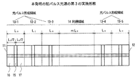
図4は、本発明の短パルス光源の第3の実施形態を示す。
本実施形態における半導体レーザ共振器は、第1の共振器端面11から第2の共振器端面12へ向けて、順に3つの光パルス形成領域13−1,13−2,13−3、利得領域14、2つの光パルス形成領域13−4,13−5の各領域が配置された構成になっている。このように、利得領域14の両側に配置される光パルス形成領域13は、必ずしも同数である必要はない。
(Third embodiment)
FIG. 4 shows a third embodiment of the short pulse light source of the present invention.
The semiconductor laser resonator according to this embodiment includes three optical pulse forming regions 13-1, 13-2, 13-3, and a gain region in order from the first
(第4の実施形態)
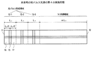
図5は、本発明の短パルス光源の第4の実施形態を示す。
本実施形態における半導体レーザ共振器は、第1の共振器端面11から第2の共振器端面12へ向けて、順に3つの光パルス形成領域13−1,13−2,13−3、利得領域14の各領域が配置された構成になっている。このように、利得領域14の片側のみに光パルス形成領域13を配置する構成としてもよい。
(Fourth embodiment)
FIG. 5 shows a fourth embodiment of the short pulse light source of the present invention.
The semiconductor laser resonator according to this embodiment includes three optical pulse forming regions 13-1, 13-2, 13-3, and a gain region in order from the first
なお、以上図示した実施形態の構成は例であり、特に光パルス形成領域13が2以上あればその数には限定されない。ただし、光パルス形成領域13の数を増やすことにより効率的な短パルス化に寄与するが、総素子長が長くなるため、1枚のウェハから得られる半導体レーザ数が減少する。また、利得領域14を長くすることにより、より高出力のパルス光を発生させることができるが、同様に1枚のウェハから得られる半導体レーザ数が減少する。素子構成の設計は、望まれるパルス光のスペック(パルス幅、繰り返し周期、出力等)と価格との兼ね合いで決定される。 The configuration of the embodiment shown above is an example, and the number is not limited as long as there are two or more optical pulse forming regions 13. However, increasing the number of optical pulse forming regions 13 contributes to efficient shortening of the pulse, but the total element length is increased, so the number of semiconductor lasers obtained from one wafer is reduced. Further, by making the gain region 14 longer, higher-power pulsed light can be generated, but the number of semiconductor lasers obtained from one wafer is similarly reduced. The design of the element configuration is determined in consideration of the desired specifications (pulse width, repetition period, output, etc.) of the pulsed light and the price.
11,12 共振器端面
13 光パルス形成領域
14 利得領域
15 可飽和吸収領域
16,17 活性領域 61,62 レーザ共振器端面
63 可飽和吸収領域
64 光導波路領域
66,67 電極分離溝
68 活性領域
71 可飽和吸収領域
72,73 活性領域
DESCRIPTION OF
Claims (5)
前記2以上の光パルス形成領域のそれぞれは、前記半導体レーザ共振器の光波伝搬軸上に、第1の活性領域、可飽和吸収領域、第2の活性領域の順に配置され、かつ可飽和吸収領域が光パルス形成領域の中央に配置され、衝突パルスモード同期によって短パルス光を生成する構成であり、
前記利得領域は、前記1つの光パルス形成領域の長さの正数倍である
ことを特徴とする短パルス光源。 In the Fabry-Perot type semiconductor laser resonator formed by the first and second semiconductor laser resonator end faces, one gain region and two or more optical pulse forming regions are on the light wave propagation axis of the semiconductor laser resonator. Arranged in series,
Each of the two or more optical pulse forming regions is arranged in the order of a first active region, a saturable absorption region, and a second active region on the light wave propagation axis of the semiconductor laser resonator, and the saturable absorption region. Is arranged in the center of the optical pulse forming region, and is configured to generate short pulse light by collision pulse mode synchronization,
The short pulse light source, wherein the gain region is a positive multiple of the length of the one optical pulse forming region.
前記2以上の光パルス形成領域は、前記利得領域の両側に配置された構成である
ことを特徴とする短パルス光源。 The short pulse light source according to claim 1,
The short pulse light source, wherein the two or more optical pulse forming regions are arranged on both sides of the gain region.
前記利得領域の両側に配置される前記光パルス形成領域は、それぞれ少なくとも1つあり、かつ同数である
ことを特徴とする短パルス光源。 The short pulse light source according to claim 2,
The short pulse light source characterized in that there are at least one and the same number of the optical pulse forming regions arranged on both sides of the gain region.
前記利得領域の両側に配置される前記光パルス形成領域は、それぞれ少なくとも1つあり、かつ異なる数である
ことを特徴とする短パルス光源。 The short pulse light source according to claim 2,
The short pulse light source characterized in that there are at least one and a different number of the optical pulse forming regions arranged on both sides of the gain region.
前記2以上の光パルス形成領域は、前記利得領域の片側に配置された構成である
ことを特徴とする短パルス光源。
The short pulse light source according to claim 1,
The short pulse light source characterized in that the two or more optical pulse forming regions are arranged on one side of the gain region.
Priority Applications (1)
| Application Number | Priority Date | Filing Date | Title |
|---|---|---|---|
| JP2005291468A JP2007103669A (en) | 2005-10-04 | 2005-10-04 | Short pulse light source |
Applications Claiming Priority (1)
| Application Number | Priority Date | Filing Date | Title |
|---|---|---|---|
| JP2005291468A JP2007103669A (en) | 2005-10-04 | 2005-10-04 | Short pulse light source |
Publications (1)
| Publication Number | Publication Date |
|---|---|
| JP2007103669A true JP2007103669A (en) | 2007-04-19 |
Family
ID=38030309
Family Applications (1)
| Application Number | Title | Priority Date | Filing Date |
|---|---|---|---|
| JP2005291468A Withdrawn JP2007103669A (en) | 2005-10-04 | 2005-10-04 | Short pulse light source |
Country Status (1)
| Country | Link |
|---|---|
| JP (1) | JP2007103669A (en) |
Cited By (1)
| Publication number | Priority date | Publication date | Assignee | Title |
|---|---|---|---|---|
| JP2011018784A (en) * | 2009-07-09 | 2011-01-27 | Sony Corp | Semiconductor laser element, driving method thereof, and semiconductor laser device |
-
2005
- 2005-10-04 JP JP2005291468A patent/JP2007103669A/en not_active Withdrawn
Cited By (2)
| Publication number | Priority date | Publication date | Assignee | Title |
|---|---|---|---|---|
| JP2011018784A (en) * | 2009-07-09 | 2011-01-27 | Sony Corp | Semiconductor laser element, driving method thereof, and semiconductor laser device |
| US8989228B2 (en) | 2009-07-09 | 2015-03-24 | Sony Corporation | Laser diode device, method of driving the same, and laser diode apparatus |
Similar Documents
| Publication | Publication Date | Title |
|---|---|---|
| US6853658B1 (en) | Optical logical circuits based on lasing semiconductor optical amplifiers | |
| JP6716142B2 (en) | Surface emitting laser | |
| Lai et al. | Multiple pulse operation of a femtosecond Ti: sapphire laser | |
| Fischer et al. | High single-mode power observed from a coupled-resonator vertical-cavity laser diode | |
| US20090116516A1 (en) | Mode-locked solid-state laser apparatus | |
| JP6662790B2 (en) | Optical amplifier | |
| CN105449515B (en) | A kind of semiconductor ultrashort pulse Gao Zhongying laser | |
| JP2007103669A (en) | Short pulse light source | |
| Tushar et al. | Modeling and analysis of Z folded solid state laser cavity with two curved mirrors | |
| JP2823094B2 (en) | Short pulse light source device and method of generating short pulse light | |
| Oudar et al. | Demonstration of optical bistability with intensity‐coupled high gain lasers | |
| JPH07307512A (en) | Optically driven ultrafast forced mode-locked laser system | |
| Meinecke et al. | Increasing stability by two-state lasing in quantum-dot lasers with optical injection | |
| EP3327880B1 (en) | Excimer laser system with annular chamber structure | |
| Lin et al. | Short pulse generation by electrical gain switching of vertical cavity surface emitting laser | |
| Hassan et al. | 4 W Single-Mode Operation of Surface Grating VCSELs | |
| Nielsen et al. | Investigation of unidirectionality in an asymmetric ring mode locked laser with two saturable absorbers | |
| JPH06169124A (en) | Short optical pulse generating device | |
| Xia et al. | External-cavity mode-locked quantum-dot lasers for low repetition rate, sub-picosecond pulse generation | |
| Zeng et al. | Hybrid Integration of Hook-shaped Traveling-wave Semiconductor Optical Amplifier and Taiji Ring Resonator for Unidirectional Lasing | |
| Nikkinen et al. | Microchip laser Q‐switched with GaInNAs/GaAs SESAM emitting 204 ps pulses at 1342 nm | |
| JP2019046880A (en) | Surface emitting laser | |
| JP2555951B2 (en) | Semiconductor laser | |
| Davenport et al. | A hybrid silicon/InP integrated feedback stabilized mode-locked laser | |
| JP2500604B2 (en) | Ultra high speed optical oscillator |
Legal Events
| Date | Code | Title | Description |
|---|---|---|---|
| A300 | Withdrawal of application because of no request for examination |
Free format text: JAPANESE INTERMEDIATE CODE: A300 Effective date: 20090106 |