JP2007103402A - Optical source - Google Patents
Optical source Download PDFInfo
- Publication number
- JP2007103402A JP2007103402A JP2005287309A JP2005287309A JP2007103402A JP 2007103402 A JP2007103402 A JP 2007103402A JP 2005287309 A JP2005287309 A JP 2005287309A JP 2005287309 A JP2005287309 A JP 2005287309A JP 2007103402 A JP2007103402 A JP 2007103402A
- Authority
- JP
- Japan
- Prior art keywords
- resin
- light
- light emitting
- emitting element
- light source
- Prior art date
- Legal status (The legal status is an assumption and is not a legal conclusion. Google has not performed a legal analysis and makes no representation as to the accuracy of the status listed.)
- Pending
Links
Images


Classifications
-
- H—ELECTRICITY
- H01—ELECTRIC ELEMENTS
- H01L—SEMICONDUCTOR DEVICES NOT COVERED BY CLASS H10
- H01L2224/00—Indexing scheme for arrangements for connecting or disconnecting semiconductor or solid-state bodies and methods related thereto as covered by H01L24/00
- H01L2224/01—Means for bonding being attached to, or being formed on, the surface to be connected, e.g. chip-to-package, die-attach, "first-level" interconnects; Manufacturing methods related thereto
- H01L2224/42—Wire connectors; Manufacturing methods related thereto
- H01L2224/47—Structure, shape, material or disposition of the wire connectors after the connecting process
- H01L2224/48—Structure, shape, material or disposition of the wire connectors after the connecting process of an individual wire connector
- H01L2224/4805—Shape
- H01L2224/4809—Loop shape
- H01L2224/48091—Arched
Landscapes
- Led Device Packages (AREA)
Abstract
Description
本発明は、発光素子と発光素子の光によって励起されて光を発する蛍光剤の組み合わせによって発光を行う光源に関する。 The present invention relates to a light source that emits light by a combination of a light emitting element and a fluorescent agent that emits light when excited by light of the light emitting element.
特許文献1には、青色の光を発する発光素子と、この発光素子を覆う透明な樹脂の中に青色の光によって励起されて黄色の光を発する蛍光剤を含有させ、青色と黄色の混色によって白色の発光を行う光源が開示されている。
In
青色と黄色の混色による白色発光の場合、赤、緑、青色の成分の内、赤色成分が少ないので、液晶表示装置のバックライトやカメラのフラッシュ用途においては、色再現性に課題を有していた。 In the case of white light emission with a mixed color of blue and yellow, there are few red components among red, green, and blue components, so there is a problem in color reproducibility in backlights of liquid crystal display devices and camera flashes. It was.
赤色成分の不足を補うために、赤色発光素子を追加することを検討したが、赤色の光が蛍光剤によって不必要に拡散されたり、赤色の光の透過性が低下したりする。緑色成分を増加させるために、蛍光剤として、青色励起の緑色発光のものを用いても同様の課題がある。
本発明は、樹脂中に含有させた蛍光剤が、この蛍光剤の励起光源として用いられる発光素子以外の発光素子の光へ与える悪影響を排除することを課題の1つとする。色再現性の良い白色の光源を提供することを課題の1つとする。 An object of the present invention is to eliminate an adverse effect of a fluorescent agent contained in a resin on light of a light emitting element other than a light emitting element used as an excitation light source of the fluorescent agent. It is an object to provide a white light source with good color reproducibility.
本発明の光源は、請求項1に記載のように、第1、第2の色を発光する第1、第2の発光素子と、前記第1の発光色によって励起されて第3の色を発光する蛍光剤と、前記蛍光剤を含有するとともに前記第1の発光素子を覆う第1の樹脂と、第1の樹脂とこの第1樹脂の外側に配置される前記第2発光素子を覆う第2樹脂を備え、前記第1、第2、第3の発光色を混色させた光を発光色として用いることを特徴とする。
As described in
本発明の光源は、請求項2に記載のように、前記第1の樹脂と接する第1の壁面と、前記第2の樹脂と接する第2の壁面を備え、前記第2の壁面の高さを第1の壁面の高さよりも高くすることができる。
As described in
本発明の光源は、請求項3に記載のように、前記第1、第2の樹脂を第1、第2の高さを持つ半球状とし、前記第2の樹脂の高さを、前記第1の樹脂の高さよりも高くすることができる。
According to a light source of the present invention, as described in
本発明の光源は、請求項4に記載のように、前記第1の発光色を青色、前記第2の発光色を赤色、第3の発光色を緑色とすることができる。
As described in
本発明の光源は、請求項5に記載のように、前記半球状の光源を基板に複数配列することができる。
In the light source of the present invention, as described in
本発明の光源は、請求項6に記載のように、前記基板の上に枠を設け、この枠に前記第2の樹脂を囲む反射面を設け、この反射面と前記第2の樹脂の間に空気層を介在させることができる。
According to the light source of the present invention, as described in
蛍光剤による拡散や遮光の発生を防ぎ色再現性の良い光源を提供することができる。 It is possible to provide a light source with good color reproducibility by preventing the occurrence of diffusion and shading due to the fluorescent agent.
以下本発明の実施形態を図面を参照して説明する。 Embodiments of the present invention will be described below with reference to the drawings.
図1は水平方向発光型の光源(第1の実施形態)を示す斜視図、図2は図1のS1−S2に沿った断面図である。この光源1は、平板状の樹脂からなるパッケージ2の正面中央に矩形の発光窓3を設け、左右の側面から底面にかかる領域並びに背面に電極4,5,6を設けている。
FIG. 1 is a perspective view showing a horizontal light-emitting type light source (first embodiment), and FIG. 2 is a cross-sectional view taken along S1-S2 in FIG. In this
図2に示すように、パッケージ2には、発光窓3から内側に向けて第1の窪み7が形成され、この窪み7の内壁面に前記電極4,5,6の一部が露出している。第1の窪み7の中に発光色が異なる第1、第2の発光素子8,9が配置されている。第1の発光素子8は青色の発光色を持ち、電極5の上に配置され、電極4,5にワイヤーボンド配線が施されている。第2の発光素子9は赤色の発光色を持ち、電極5の上に配置され、電極6にワイヤーボンド配線が施されている。
As shown in FIG. 2, the
窪み7の中には、第1の発光素子8を囲むように、第1の窪み7より一回り小さな第2の窪み10が形成されている。この第2の窪み10には、蛍光剤を含有した第1の樹脂11が満たされている。第1の樹脂11は透明な樹脂で構成され、その中に蛍光剤が分散して配置される。第1の樹脂11中の蛍光剤は、第1の発光素子8が発する光(励起光)によって励起されて、励起光よりも波長が長い光、この例では緑色の光を発する。
A
第1の窪み7は、第2の樹脂12が充填されている。第2の樹脂12は、第1の樹脂11と、この第1の樹脂11とは隔離して配置された第2の発光素子9の両方を覆う透明な樹脂である。第2の発光素子9が、第1の樹脂11と隔離して配置されているので、第2の発光素子9の光が第1の樹脂11中の蛍光剤によって不必要に拡散されたり遮光されたりする不都合を解消することが出来る。
The
第1の樹脂11と接するパッケージ2の壁面の高さよりも、第2の樹脂12と接するパッケージ2の壁面の高さが高く設定されている。第1、第2の樹脂11、12の一方あるいは両方の中に、必要に応じて光拡散材を含有させることもできる。
The height of the wall surface of the
第1の発光素子8が発した光の一部は、第1の樹脂11と第2の樹脂12を通り、発光窓3から外に出る。第1の発光素子8が発した光の一部は、第1の樹脂11中の蛍光剤の励起光として作用する。励起された蛍光剤から発した光は、第1、第2の樹脂11,12を通って発光窓3から外に出る。第2の発光素子9の光は、第2の樹脂12を通って発光窓3から外にでる。発光窓3から出射されるこれらの光は、合成光として認識される。この例では、青色と赤色と緑色の光が合成されて、白色系の合成光が得られる。
Part of the light emitted from the first
先の実施形態は、水平方向発光型の光源への適用例であったが、垂直方向発光型の光源への適用例を図3,4を参照して説明する。 The previous embodiment was an application example to a horizontal light emission type light source, but an application example to a vertical light emission type light source will be described with reference to FIGS.
図3は垂直方向発光型の光源(第2の実施形態)を示す斜視図、図4は図3のS3−S4に沿った断面図である。この光源1は、直方体形状の樹脂からなるパッケージ2の天面中央に矩形の発光窓3を設け、左右の側面から底面にかかる領域に電極4,5,6を設けている。
FIG. 3 is a perspective view showing a vertical light emitting type light source (second embodiment), and FIG. 4 is a cross-sectional view taken along S3-S4 in FIG. In this
図4に示すように、パッケージ2には、発光窓3から内側に向けて第1の窪み7が形成され、この窪み7の内壁面に前記電極4,5,6の一部が露出している。第1の窪み7の中に発光色が異なる第1、第2の発光素子8,9が配置されている。第1の発光素子8は青色の発光色を持ち、電極5の上に配置され、電極4,5にワイヤーボンド配線が施されている。第2の発光素子9は赤色の発光色を持ち、電極5の上に配置され、電極5,6にワイヤーボンド配線が施されている。
As shown in FIG. 4, a
窪み7の中には、第1の発光素子を囲むように、窪みより一回り小さな第2の窪み10が形成されている。この第2の窪み10には、蛍光剤を含有した第1の樹脂11が満たされている。蛍光剤は、第1の発光素子8が発する光(励起光)によって励起されて、励起光よりも波長が長い光、この例では緑色の光を発する。
A
第1の窪み7は、第2の樹脂12が充填されている。第2の樹脂12は、第1の樹脂11と、この第1の樹脂11とは隔離して配置された第2の発光素子9の両方を覆う。第2の発光素子9が、第1の樹脂11と隔離して配置されているので、第2の発光素子9の光が第1の樹脂11中の蛍光剤によって不必要に拡散されたり遮光されたりする不都合を解消することが出来る。
The
第1の発光素子8から発した光の一部は、第1、第2の樹脂11,12を通って発光窓から外に出る。第1の発光素子8から発した光の一部は、蛍光剤の励起光として作用する。励起された蛍光剤から発した光は、第1、第2の樹脂11,12を通って発光窓3から外に出る。第2の発光素子の光は、第2の樹脂を通って発光窓3の外にでる。発光窓3から出射されるこれらの光が合成されて、白色系の光が得られる。
Part of the light emitted from the first
次に、第1、第2の発光素子8,9を半球状の樹脂によってモールドした実施形態について図5,6を参照して説明する。
Next, an embodiment in which the first and second
図5は垂直方向発光型の光源(第3の実施形態)を示す平面図、図6は図5のS5−S6に沿った断面図である。この光源1は、矩形の回路基板13上に、発光窓3として機能する樹脂枠14を重ねて配置したパッケージ2を備えている。回路基板13は、図示していないが、表面に回路パターンを有しているとともに、側面から裏面にかけてスルーホール形態の電極を設けている。回路基板13の中央部に発光色が相違する第1、第2の発光素子8,9が配置され、ワイヤーボンド配線などの配線(図示を省略)が施されている。第1の発光素子8は蛍光剤を含有する半球状の第1の樹脂11で覆われている。第2の発光素子9は、この第1の樹脂11の外側に配置され、第1の樹脂11と第2の発光素子9はともに半球状の透明な第2の樹脂12で覆われている。第1、第2の樹脂11,12はともに、図1−4に示す実施形態のような窪みに配置するのではなく、平面上に盛り上がった状態で配置される。第1の樹脂11の高さ(第1の高さ)と、第2の樹脂12の高さ(第2の高さ)は、第2の高さが第1の高さよりも高くなるようにしている。
FIG. 5 is a plan view showing a vertical light source (third embodiment), and FIG. 6 is a cross-sectional view taken along S5-S6 in FIG. The
樹脂11,12の形状は、樹脂の粘度や硬化条件を調整することによって半球状やそれに類する形状に設定することができる。また、半球状に類する樹脂11,12の形状として、円錐形状、四角錐形状、多角錐形状、円柱形状、四角柱形状、多角柱形状、円柱の天面に逆円錐形状の窪みを設けた形状(断面M形状)、ふたこぶ形状などに設定することもできる。
The shape of the
樹脂枠14は、中央に発光窓3を設けている。発光窓3は、樹脂枠14の底部から天面に向けて外側に傾斜した反射面15を備えている。この反射面15は、平面視で多角形、この例では8角形状としているが、その他の多角形や円形とすることもできる。樹脂枠14は白色樹脂として反射性を高めているが、反射面15に光反射性に優れる金属板や金属薄膜などを一体的に形成しても良い。反射面15と樹脂12の間は離間され、その間に空気層が介在する形態としている。
The
図5,6に示す実施形態においても、第2発光素子9の発する光が第1樹脂11中の蛍光剤によって拡散されたり、遮光されたりする不具合を回避することが出来る。
In the embodiment shown in FIGS. 5 and 6, it is possible to avoid the problem that the light emitted from the second
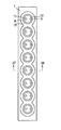
図7に示す実施形態は、図5,6に示す光源を一列に配列した形態を持つ線状の光源を示す。基板13と樹脂枠14の形態に変更がある他は、図5,6に示す構成と実質同一構成をとる(同一部分は同一の図番を付している)。よってS7−S8に沿った断面図は、図6に示す断面図と同じになる。尚、第1の発光素子8が一方(この例では左側)、第2の発光素子9が他方(この例では右側)に偏って配置されると、色むらの原因になる可能性もあるので、色むらを防ぐために光源の位置によって光源の中の発光素子の配置を変化させても良い。光源内の発光素子の配置は、図8に示すように180度回転させた形態の他に、90度、60度などの様に、所定角度ずつの回転ずれを有する形態で配置することもできる。
The embodiment shown in FIG. 7 shows a linear light source having a form in which the light sources shown in FIGS. Except that there is a change in the form of the
図8に示す実施形態は、図5,6に示す光源を2次元(マトリックス状)に配列した形態を持つ面状の光源を示す。基板13と樹脂枠14の形態に変更がある他は、図5,6に示す構成と実質同一構成をとる(同一部分は同一の図番を付している)。先の実施形態と同様に、第1の発光素子8が一方、第2の発光素子9が他方に偏って配置されると、色むらの原因になる可能性もある。そこで、色むらを防ぐために光源の位置によって光源の中の発光素子の配置を変化させている。すなわち、内部の発光素子(この例では第1、第2の発光素子)の相対的な位置が相違する複数種類の光源を設け、この種類の相違する光源を分散して配列している。
The embodiment shown in FIG. 8 shows a planar light source having a form in which the light sources shown in FIGS. 5 and 6 are arranged two-dimensionally (matrix). Except that there is a change in the form of the
上記実施形態において、発光素子8,9は各々が1つの素子に限らず、複数個としても良い。また、上記実施形態は青色光励起緑色発光の蛍光剤を例示したが、青色光励起赤色発光の蛍光剤励起等、励起光源と蛍光剤の組み合わせは、上記の例に限定されず、他の組み合わせとすることもできる。
In the above embodiment, each of the
また、図5〜8に示す実施形態において、樹脂枠14を省略することもできる。すなわち、基板13上に樹脂で複数の発光素子を覆った光源部分を1つ、あるいは線状に、あるいは2次元配置した光源とすることもできる。
In the embodiment shown in FIGS. 5 to 8, the
蛍光剤による波長変換を行う光源に適用することができる。 The present invention can be applied to a light source that performs wavelength conversion using a fluorescent agent.
1 光源
2 パッケージ
3 発光窓
7 第1の窪み
8 第1の発光素子
9 第2の発光素子
10 第2の窪み
11 第1の樹脂
12 第2の樹脂
DESCRIPTION OF
Claims (6)
Priority Applications (1)
| Application Number | Priority Date | Filing Date | Title |
|---|---|---|---|
| JP2005287309A JP2007103402A (en) | 2005-09-30 | 2005-09-30 | Optical source |
Applications Claiming Priority (1)
| Application Number | Priority Date | Filing Date | Title |
|---|---|---|---|
| JP2005287309A JP2007103402A (en) | 2005-09-30 | 2005-09-30 | Optical source |
Publications (1)
| Publication Number | Publication Date |
|---|---|
| JP2007103402A true JP2007103402A (en) | 2007-04-19 |
Family
ID=38030099
Family Applications (1)
| Application Number | Title | Priority Date | Filing Date |
|---|---|---|---|
| JP2005287309A Pending JP2007103402A (en) | 2005-09-30 | 2005-09-30 | Optical source |
Country Status (1)
| Country | Link |
|---|---|
| JP (1) | JP2007103402A (en) |
Cited By (12)
| Publication number | Priority date | Publication date | Assignee | Title |
|---|---|---|---|---|
| JP2008305992A (en) * | 2007-06-07 | 2008-12-18 | Sharp Corp | Light emitting device and cellular phone with camera loaded with the same |
| JP2010098313A (en) * | 2008-10-15 | 2010-04-30 | Samsung Led Co Ltd | Led package module |
| JP2011066108A (en) * | 2009-09-16 | 2011-03-31 | Mitsubishi Electric Corp | Light-emitting device and illuminator |
| JP2012059737A (en) * | 2010-09-03 | 2012-03-22 | Panasonic Corp | Light emitting device, backlight unit, liquid crystal display device, and lighting system |
| JP2012059736A (en) * | 2010-09-03 | 2012-03-22 | Panasonic Corp | Light-emitting device, backlight unit, liquid crystal display device, and illumination device |
| JP2013012529A (en) * | 2011-06-28 | 2013-01-17 | Citizen Electronics Co Ltd | Led package |
| KR20130011883A (en) * | 2011-07-20 | 2013-01-30 | 엘지디스플레이 주식회사 | Light emitting device, light emitting device package, and backlihgt unit |
| JP2013529841A (en) * | 2010-06-16 | 2013-07-22 | オスラム オプト セミコンダクターズ ゲゼルシャフト ミット ベシュレンクテル ハフツング | Optoelectronic element |
| JP2013258399A (en) * | 2012-05-16 | 2013-12-26 | Rohm Co Ltd | Led light source module and method of manufacturing the same |
| KR20140061792A (en) * | 2012-11-14 | 2014-05-22 | 삼성전자주식회사 | Light emitting device package and manufacturing method therof |
| JP2015149515A (en) * | 2015-05-28 | 2015-08-20 | シャープ株式会社 | Light-emitting device and illumination apparatus |
| JP2017054996A (en) * | 2015-09-10 | 2017-03-16 | パナソニックIpマネジメント株式会社 | Light emitting device and luminaire |
-
2005
- 2005-09-30 JP JP2005287309A patent/JP2007103402A/en active Pending
Cited By (15)
| Publication number | Priority date | Publication date | Assignee | Title |
|---|---|---|---|---|
| JP2008305992A (en) * | 2007-06-07 | 2008-12-18 | Sharp Corp | Light emitting device and cellular phone with camera loaded with the same |
| JP2010098313A (en) * | 2008-10-15 | 2010-04-30 | Samsung Led Co Ltd | Led package module |
| JP2011066108A (en) * | 2009-09-16 | 2011-03-31 | Mitsubishi Electric Corp | Light-emitting device and illuminator |
| US8759862B2 (en) | 2010-06-16 | 2014-06-24 | Osram Opto Semiconductors Gmbh | Optoelectronic component |
| JP2013529841A (en) * | 2010-06-16 | 2013-07-22 | オスラム オプト セミコンダクターズ ゲゼルシャフト ミット ベシュレンクテル ハフツング | Optoelectronic element |
| JP2012059737A (en) * | 2010-09-03 | 2012-03-22 | Panasonic Corp | Light emitting device, backlight unit, liquid crystal display device, and lighting system |
| JP2012059736A (en) * | 2010-09-03 | 2012-03-22 | Panasonic Corp | Light-emitting device, backlight unit, liquid crystal display device, and illumination device |
| JP2013012529A (en) * | 2011-06-28 | 2013-01-17 | Citizen Electronics Co Ltd | Led package |
| KR20130011883A (en) * | 2011-07-20 | 2013-01-30 | 엘지디스플레이 주식회사 | Light emitting device, light emitting device package, and backlihgt unit |
| KR101946313B1 (en) * | 2011-07-20 | 2019-02-12 | 엘지디스플레이 주식회사 | Light emitting device, light emitting device package, and backlihgt unit |
| JP2013258399A (en) * | 2012-05-16 | 2013-12-26 | Rohm Co Ltd | Led light source module and method of manufacturing the same |
| KR20140061792A (en) * | 2012-11-14 | 2014-05-22 | 삼성전자주식회사 | Light emitting device package and manufacturing method therof |
| KR101957701B1 (en) * | 2012-11-14 | 2019-03-14 | 삼성전자주식회사 | Light emitting device package and manufacturing method therof |
| JP2015149515A (en) * | 2015-05-28 | 2015-08-20 | シャープ株式会社 | Light-emitting device and illumination apparatus |
| JP2017054996A (en) * | 2015-09-10 | 2017-03-16 | パナソニックIpマネジメント株式会社 | Light emitting device and luminaire |
Similar Documents
| Publication | Publication Date | Title |
|---|---|---|
| JP2007103402A (en) | Optical source | |
| US9632355B2 (en) | Display device | |
| JP6639081B2 (en) | Light source module | |
| JP5980577B2 (en) | Side-illuminated LED light-emitting device and method for manufacturing side-illuminated LED light-emitting device | |
| JP4629023B2 (en) | Surface light source device and display device | |
| WO2012002029A1 (en) | Illumination device, display device, television receiving device, and led light source | |
| US20080123021A1 (en) | Light emitting diode package, backlight unit and liquid crystal display having the same | |
| JP7231832B2 (en) | Light-emitting device, liquid crystal display device | |
| JP2009200534A (en) | Semiconductor light emitting device | |
| KR20100086692A (en) | Backlight unit and display apparatus having the same | |
| JP2007180524A (en) | Reflector frame, surface light source device provided with same, and display device using surface light source device | |
| TW202144823A (en) | Light emitting module and planar light source | |
| JP2019153436A (en) | Luminaire and display device | |
| JP2007095674A (en) | Plane light source device and display device | |
| JP5108297B2 (en) | Light emitting element mounting package, surface light source device, and display device | |
| WO2012032978A1 (en) | Reflective sheet, lighting device, and display device | |
| JP7231845B2 (en) | Light source device | |
| CN111211210A (en) | Light emitting device | |
| JP2022082802A (en) | Light emitting device | |
| WO2011067987A1 (en) | Light source package, illumination device, display device, and television receiving device | |
| JP2011034674A (en) | Planar light source and illuminated signboard | |
| JP4594859B2 (en) | LIGHTING DEVICE AND IMAGE DISPLAY DEVICE USING THE SAME | |
| US10495922B2 (en) | Display device | |
| JP2023118824A (en) | Reflection member and light source device | |
| KR101454608B1 (en) | Display device |