JP2007027461A - Core and inductor with core - Google Patents
Core and inductor with core Download PDFInfo
- Publication number
- JP2007027461A JP2007027461A JP2005208243A JP2005208243A JP2007027461A JP 2007027461 A JP2007027461 A JP 2007027461A JP 2005208243 A JP2005208243 A JP 2005208243A JP 2005208243 A JP2005208243 A JP 2005208243A JP 2007027461 A JP2007027461 A JP 2007027461A
- Authority
- JP
- Japan
- Prior art keywords
- core
- inductor
- electrode
- substrate
- top surface
- Prior art date
- Legal status (The legal status is an assumption and is not a legal conclusion. Google has not performed a legal analysis and makes no representation as to the accuracy of the status listed.)
- Pending
Links
- 238000004804 winding Methods 0.000 claims description 18
- 239000000758 substrate Substances 0.000 abstract description 34
- 239000000853 adhesive Substances 0.000 abstract description 2
- 230000001070 adhesive effect Effects 0.000 abstract description 2
- 239000011162 core material Substances 0.000 description 67
- 229910000679 solder Inorganic materials 0.000 description 15
- PXHVJJICTQNCMI-UHFFFAOYSA-N Nickel Chemical compound [Ni] PXHVJJICTQNCMI-UHFFFAOYSA-N 0.000 description 8
- 229910000859 α-Fe Inorganic materials 0.000 description 6
- 230000002093 peripheral effect Effects 0.000 description 5
- BQCADISMDOOEFD-UHFFFAOYSA-N Silver Chemical compound [Ag] BQCADISMDOOEFD-UHFFFAOYSA-N 0.000 description 4
- 229910052759 nickel Inorganic materials 0.000 description 4
- 229910052709 silver Inorganic materials 0.000 description 4
- 239000004332 silver Substances 0.000 description 4
- PWHULOQIROXLJO-UHFFFAOYSA-N Manganese Chemical compound [Mn] PWHULOQIROXLJO-UHFFFAOYSA-N 0.000 description 3
- 239000000696 magnetic material Substances 0.000 description 3
- 229910052748 manganese Inorganic materials 0.000 description 3
- 239000011572 manganese Substances 0.000 description 3
- 239000000463 material Substances 0.000 description 3
- 238000007747 plating Methods 0.000 description 3
- 239000010409 thin film Substances 0.000 description 3
- 229910000976 Electrical steel Inorganic materials 0.000 description 2
- 229910052751 metal Inorganic materials 0.000 description 2
- 239000002184 metal Substances 0.000 description 2
- 238000000034 method Methods 0.000 description 2
- 229910000889 permalloy Inorganic materials 0.000 description 2
- 229910000702 sendust Inorganic materials 0.000 description 2
- 238000007740 vapor deposition Methods 0.000 description 2
- RYGMFSIKBFXOCR-UHFFFAOYSA-N Copper Chemical compound [Cu] RYGMFSIKBFXOCR-UHFFFAOYSA-N 0.000 description 1
- 239000004642 Polyimide Substances 0.000 description 1
- HCHKCACWOHOZIP-UHFFFAOYSA-N Zinc Chemical compound [Zn] HCHKCACWOHOZIP-UHFFFAOYSA-N 0.000 description 1
- 230000015572 biosynthetic process Effects 0.000 description 1
- 229910052802 copper Inorganic materials 0.000 description 1
- 239000010949 copper Substances 0.000 description 1
- 239000010408 film Substances 0.000 description 1
- 230000004927 fusion Effects 0.000 description 1
- 150000002739 metals Chemical class 0.000 description 1
- 230000003647 oxidation Effects 0.000 description 1
- 238000007254 oxidation reaction Methods 0.000 description 1
- 239000003973 paint Substances 0.000 description 1
- 229920001721 polyimide Polymers 0.000 description 1
- 229920006395 saturated elastomer Polymers 0.000 description 1
- 238000005728 strengthening Methods 0.000 description 1
- 238000007751 thermal spraying Methods 0.000 description 1
- 229910052725 zinc Inorganic materials 0.000 description 1
- 239000011701 zinc Substances 0.000 description 1
Images


Classifications
-
- H—ELECTRICITY
- H01—ELECTRIC ELEMENTS
- H01F—MAGNETS; INDUCTANCES; TRANSFORMERS; SELECTION OF MATERIALS FOR THEIR MAGNETIC PROPERTIES
- H01F27/00—Details of transformers or inductances, in general
- H01F27/24—Magnetic cores
- H01F27/26—Fastening parts of the core together; Fastening or mounting the core on casing or support
-
- H—ELECTRICITY
- H01—ELECTRIC ELEMENTS
- H01F—MAGNETS; INDUCTANCES; TRANSFORMERS; SELECTION OF MATERIALS FOR THEIR MAGNETIC PROPERTIES
- H01F27/00—Details of transformers or inductances, in general
- H01F27/28—Coils; Windings; Conductive connections
- H01F27/29—Terminals; Tapping arrangements for signal inductances
- H01F27/292—Surface mounted devices
-
- H—ELECTRICITY
- H01—ELECTRIC ELEMENTS
- H01F—MAGNETS; INDUCTANCES; TRANSFORMERS; SELECTION OF MATERIALS FOR THEIR MAGNETIC PROPERTIES
- H01F3/00—Cores, Yokes, or armatures
- H01F3/10—Composite arrangements of magnetic circuits
- H01F3/14—Constrictions; Gaps, e.g. air-gaps
-
- H—ELECTRICITY
- H01—ELECTRIC ELEMENTS
- H01F—MAGNETS; INDUCTANCES; TRANSFORMERS; SELECTION OF MATERIALS FOR THEIR MAGNETIC PROPERTIES
- H01F17/00—Fixed inductances of the signal type
- H01F17/04—Fixed inductances of the signal type with magnetic core
- H01F17/043—Fixed inductances of the signal type with magnetic core with two, usually identical or nearly identical parts enclosing completely the coil (pot cores)
-
- H—ELECTRICITY
- H01—ELECTRIC ELEMENTS
- H01F—MAGNETS; INDUCTANCES; TRANSFORMERS; SELECTION OF MATERIALS FOR THEIR MAGNETIC PROPERTIES
- H01F17/00—Fixed inductances of the signal type
- H01F17/04—Fixed inductances of the signal type with magnetic core
- H01F17/045—Fixed inductances of the signal type with magnetic core with core of cylindric geometry and coil wound along its longitudinal axis, i.e. rod or drum core
-
- H—ELECTRICITY
- H01—ELECTRIC ELEMENTS
- H01F—MAGNETS; INDUCTANCES; TRANSFORMERS; SELECTION OF MATERIALS FOR THEIR MAGNETIC PROPERTIES
- H01F41/00—Apparatus or processes specially adapted for manufacturing or assembling magnets, inductances or transformers; Apparatus or processes specially adapted for manufacturing materials characterised by their magnetic properties
- H01F41/02—Apparatus or processes specially adapted for manufacturing or assembling magnets, inductances or transformers; Apparatus or processes specially adapted for manufacturing materials characterised by their magnetic properties for manufacturing cores, coils, or magnets
- H01F41/04—Apparatus or processes specially adapted for manufacturing or assembling magnets, inductances or transformers; Apparatus or processes specially adapted for manufacturing materials characterised by their magnetic properties for manufacturing cores, coils, or magnets for manufacturing coils
- H01F41/10—Connecting leads to windings
Abstract
Description
本発明は、携帯電話、パソコン、テレビ等の各種電気機器に用いられるインダクタに関する。 The present invention relates to an inductor used in various electric devices such as a mobile phone, a personal computer, and a television.
従来から、巻線が巻回されるドラムコアの外側を覆うようにリングコアを配置し、当該リングコアの端面に直接メッキ等により電極が形成された実装タイプのインダクタが存在する。このようなタイプのインダクタとしては、例えば特許文献1のようようなものが知られている。 Conventionally, there is a mounting type inductor in which a ring core is disposed so as to cover the outside of a drum core around which a winding is wound, and an electrode is directly formed on an end surface of the ring core by plating or the like. As this type of inductor, for example, one disclosed in Patent Document 1 is known.
ところで、特許文献1記載のインダクタでは、コア端面に凸部を設け、当該凸部に導電性のペースト等を施すことで電極が形成されている。 By the way, in the inductor described in Patent Document 1, a convex portion is provided on the core end surface, and an electrode is formed by applying a conductive paste or the like to the convex portion.
しかしながら、特許文献1記載のインダクタでは、電極部分の凸部は頂面と側面とを有し、当該頂面と側面との境界はエッジを形成している。特許文献1記載のインダクタと基板との固着を、より強固にし、当該エッジ部分から電極をより剥がれにくくすることが要望されている。 However, in the inductor described in Patent Document 1, the convex portion of the electrode portion has a top surface and a side surface, and the boundary between the top surface and the side surface forms an edge. There is a demand for further strengthening the fixation between the inductor and the substrate described in Patent Document 1 and making the electrode more difficult to peel off from the edge portion.
本発明は上記の事情にもとづきなされたもので、その目的とするところは、基板との固着をより強固にし、より剥がれにくいコアおよびインダクタを提供しようとするものである。 The present invention has been made on the basis of the above circumstances, and an object of the present invention is to provide a core and an inductor that are more firmly fixed to a substrate and are less likely to peel off.
上記課題を解決するために、本発明は、基板に実装されるコアにおいて、
コアの端面から突出し、最も突出した部分であり平面形状となる頂面と、当該頂面の外縁から上記コアの端面に渡って形成される段部と、を有する凸部と、
頂面および段部の表面に形成される導電性の被膜と、を有する電極形成部を具備するものである。
In order to solve the above problems, the present invention provides a core mounted on a substrate,
A convex portion that protrudes from the end surface of the core, has a top surface that is the most protruding portion and has a planar shape, and a step formed from the outer edge of the top surface to the end surface of the core;
And an electrode forming portion having a conductive film formed on the top surface and the surface of the step portion.
このように構成した場合には、凸部における頂部と段部に電極が形成されるため、半田等の導電性融着材によって広い面積にてコアを基板に固着することが可能となる。したがって、コアと基板との間における接触不良を防止できると共に、コアの基板に対する固着強度を大きくできる。 In such a configuration, since the electrodes are formed on the top and step portions of the convex portion, the core can be fixed to the substrate in a wide area by a conductive fusing material such as solder. Therefore, it is possible to prevent a contact failure between the core and the substrate, and to increase the fixing strength of the core to the substrate.
また、他の発明は、上述の発明に加えて更に、頂面と段部の境界となる頂面の外縁はR形状となっているものである。このように構成した場合には、頂面の外縁はR形状となっているので、コアを基板に配置させた場合、外縁部分と基板との間に隙間ができる。したがって、半田等によりコアを基板に固定する場合、当該隙間部分に半田等が入り込み、いわゆる半田フィレットが形成される。したがって、コアの基板に対する固着強度がさらに向上する。 In another invention, in addition to the above-described invention, the outer edge of the top surface which becomes the boundary between the top surface and the stepped portion has an R shape. In such a configuration, the outer edge of the top surface has an R shape, so that when the core is disposed on the substrate, a gap is formed between the outer edge portion and the substrate. Therefore, when the core is fixed to the substrate with solder or the like, the solder or the like enters the gap portion to form a so-called solder fillet. Therefore, the fixing strength of the core to the substrate is further improved.
また、他の発明は、上述の発明に加えて更に、コアをリングコアとし、当該リングコアの内部に巻線が巻回されるドラムコアを配置し、巻線の両端を電極形成部に接続するものである。このように構成した場合には、コアの内部に巻線が巻回されたドラムコアを配置することでインダクタが形成される。したがって、半田等によりインダクタを基板に固定する場合、コアの外縁部分と基板との間に形成される隙間部分に半田等が入り込み、半田フィレットが形成されるため、コアの基板に対する固着強度が向上する。 Further, in addition to the above-described invention, another invention is such that a core is a ring core, a drum core around which a winding is wound is disposed inside the ring core, and both ends of the winding are connected to the electrode forming portion. is there. In such a configuration, an inductor is formed by disposing a drum core around which a winding is wound inside the core. Therefore, when the inductor is fixed to the substrate by solder or the like, the solder enters into the gap formed between the outer edge portion of the core and the substrate, and a solder fillet is formed, so that the strength of fixing the core to the substrate is improved. To do.
本発明によると、コアおよびインダクタの基板に対する固着をより強固にし、より剥がれにくくすることが可能となる。 According to the present invention, the core and the inductor can be more firmly fixed to the substrate, and can be more difficult to peel off.
以下、本発明の一実施の形態に係るインダクタ10について、図1から図7に基づいて説明する。本発明に係るインダクタは、面実装タイプのインダクタであり、図1は、本発明の一実施の形態に係るインダクタ10の構成を示す分解斜視図であり、面実装されない面を上方にした状態を示す図である。また、図2は、インダクタ10の平面図であり、面実装されない面から見た状態を示す図である。また、図3は、インダクタ10の構成を示す斜視図であり、面実装される面を上方にした状態を示す斜視図である。さらに、図4は、インダクタ10の構成を示す平面図であり、面実装される面から見た状態を示す図である。図5は、図3のインダクタ10をK−K線に沿って切断した断面図であり、電極凸部52b近傍を示す図である。図6は、インダクタ10の側断面図である。また、図7は、インダクタ10を基板に実装した場合の電極形成部53の状態を示す部分断面図であり、図6のXで示す部分を拡大して示す図である。なお、以下の説明においては、上方側(上端側)とは、後述する上フランジ部22が存在する側を指し、下方側(下端側)とは、後述する下フランジ部23が存在する側を指すものとする。
Hereinafter, an
上述したように、インダクタ10は、面実装タイプのインダクタであり、ドラムコア20と、銅製の巻線30と、リングコア40とから主に構成されている。
As described above, the
ドラムコア20は、リングコア40の内部に配置される。図1に示すように、ドラムコア20は、円柱形状の巻軸21と、巻軸21の上下方向両端に形成された略円板状の上フランジ部22及び下フランジ部23とを有している。上フランジ部22の外径は下フランジ部23の外径よりも大きく形成されている。このドラムコア20は、導電性を有するマンガン系のフェライト等の磁性材から形成されている。また、ドラムコア20の表面には、非導電性の非磁性材料であるポリイミド系の絶縁塗料が塗布されることにより絶縁層(不図示)が形成されている。
The
図1に示すように、巻軸21の外周には、巻線30が巻回されている。下フランジ23の側面には、巻線30の末端を引き出すための引き出し溝25が対向するように2箇所に形成されている。引き出し溝25は、下フランジ23の周側面から巻軸21の中心に向かって略楕円状に切り欠かれるように形成されている。本実施の形態では、巻線30の直径は0.02〜0.04mmとされているが、これに限られるものではない。
As shown in FIG. 1, a winding 30 is wound around the outer periphery of the
リングコア40は、図1に示すように、略四角柱の形状をしており、ニッケル系のフェライト等の磁性材から形成されている。また、リングコア40の略四角柱の対向する2つの角部には半六角形状に切り欠かれた切欠部42が形成されており、中央にはドラムコア20および巻線30を収容するための円柱状の中空部となる収容部44が形成されている。また、リングコア40の上面45の四隅には上面45から上方に向かって突出する突起部47が設けられている。このため、当該突起部47および上面45により段部49が形成されている。各突起部47の内周は、円周の一部を形成しており、突起部47の内周によって形成される円周の直径は、上フランジ部22の直径よりも大きい。また、収容部44の直径の大きさは、上フランジ22の直径よりも小さく、かつ、下フランジ部23の直径よりも大きくなっている。したがって、ドラムコア20が下フランジ部23側から収容部44に嵌め込まれることで、上フランジ部22の下面22aが段部49と当接しドラムコア20が収容部44に納められる。
As shown in FIG. 1, the
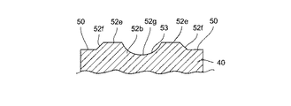
図3に示すように、リングコア40において、面実装される面となる下面50の四隅には、4つの凸部52が設けられている。以下、凸部52のうち切欠部42が形成されている側に設けられているものを補助凸部52aとし、切欠部42が形成されていない側に設けられているものを電極凸部52bとする。また、下面50において収容部44の外周部には、凸部52にも渡るようにテーパ54が形成されている。補助凸部52aは、下面50から当該下面50に対して垂直方向に突出しており、最も突出した部分は、下面50に対して水平な面となる頂面52cとなっている。また、頂面52cの両側には、補助凸部52c同士を結ぶ対角線に沿って、当該頂面52cの外縁から上面52に向かって傾斜する段部52dが形成されている。また、上述したように、補助凸部52cの収容部44側にはテーパ54が形成されている。
As shown in FIG. 3, in the
図3および図5に示すように、電極凸部52bは、リングコア40において四隅のうち切欠部42が形成されていない部位から下面50に対して垂直方向に向かって突出している。また、電極凸部52bにおいて最も突出した部分は、下面50に対して水平な面となる頂面52eとなっている。さらに、頂面52eの両側には、電極凸部52b同士を結ぶ対角線に沿う方向に、当該頂面52eの外縁から上面52に向かって傾斜する段部52fが形成されている。また、電極凸部52bの略中央には、電極凸部52b同士を結ぶ対角線に沿うように頂面52eから上方へ向かって半楕円状に切り欠かれた電極凹部52gが形成されている。本実施の形態では、補助凸部52aおよび電極凸部25bの高さは0.1〜0.3mmとされているがこれに限るものではない。
As shown in FIGS. 3 and 5, the
さらに、電極凸部52bにおいてリングコア40の外周側に相当し電極凹部52gの端部から段部52fに渡る部分は、凸状の曲面をした凸曲部52hとなっている。凸曲部52hは、リングコア40の外周部から少し内側に位置した部位から頂面52eにかけて形成されている。すなわち、リングコア40において凸曲部52hの外周側には下面50が存在する。また、インダクタ10の下面50側は、基板に面実装されるため、実装時にインダクタ10が安定するように、補助凸部52aの頂面52cの高さと電極凸部52bの頂部52eの高さは同一とされている。また、補助凸部52cと同様に、電極凸部52bの収容部44側にはテーパ54が形成されている。
Further, a portion of the
電極凸部52bは、その表面に銀の薄膜が形成されることで基板と導電可能な電極形成部53とされている。銀の薄膜は、蒸着やメッキ等の方法により電極凸部52bの表面に形成される。さらに、図3に示すように、ドラムコア20は、引き出し溝25が電極凹部52gに対向する位置となるように配置される。このため、引き出し溝25から引き出された巻線30の末端を容易に電極凹部52g上に配置することが可能となる。巻線30の末端(不図示)は、各電極凹部52g上に半田等を用いて一時的に固着される。また、ドラムコア20とリングコア40との間に形成されるギャプ55には、接着剤等が充填され、ドラムコア20とリングコア40とが一体として固定されている。
The electrode
以上のように構成されたインダクタ10では、電極凸部52bにおける頂部52eから段部52f、凸曲面52hおよびテーパ54がテーパ状に形成されると共に、当該電極凸部52bは電極形成部53となっているため、段部52fや凸曲面52hが頂部52eに対して直角に形成されている場合と比較して、広い面積にて半田等の導電性融着材を固着させることが可能となる。そのため、インダクタ10と基板との固着面積が大きくなる。したがって、インダクタ10と基板との間における接触不良を防止できると共に、インダクタ10の基板に対する固着強度を大きくできる。
In the
また、インダクタ10では、凸曲面52hは曲面形状となっているため、頂面52eと凸曲面52hとの境界はRを有する曲面となっている。したがって、半田等によりインダクタ10を基板に実装する場合、図7に示すように、基板と凸曲面52hとの間に半田等が入り込み半田フィレット60が形成される。このため、基板とインダクタ10との固着面積が大きくなり、インダクタ10の基板に対する固着強度が向上する。また、段部52fと基板との間にも半田等を充填させて半田フィレットを形成させると、さらに強固に電極形成部53を基板に固着することが可能となる。なお、インダクタ10の基板への実装は、リフローすることによって行われる。
Moreover, in the
また、インダクタ10では、頂面52eと凸曲面52hとの境界はRを有する曲面となっているため、凸曲面52hが曲面形状となっておらず平面形状であり、頂面52eと凸曲面52hとの境界がエッジを形成している場合と比較して、電極が剥がれにくくなる。したがって、インダクタ10と基板との間における接触不良を防止することが可能となる。
Further, in the
また、インダクタ10では、切欠部42が形成された2つの隅部にも補助凸部52aが形成されているため、実装状態では四隅においてインダクタ10を基板に接触させることが可能となり、安定した状態で電極形成部53を基板に実装することが可能となる。
In addition, in the
また、インダクタ10の下面側におけるドラムコア20とリングコア40との間にはギャップ55が形成されているため、インダクタ10は、磁気飽和しにくく、優れた直流重畳特性を有するものとなる。
In addition, since the
以上、本発明の一実施の形態について説明したが、本発明はこれ以外にも種々変形可能となっている。以下、それについて述べる。 Although one embodiment of the present invention has been described above, the present invention can be variously modified in addition to this. This will be described below.
上述の実施の形態では、段部52fは平坦な斜面となっているが、これに限ることなく、凸曲面状の斜面としても良い。また、電極凸部52bに形成された段部52fと凸曲面53hのうちの少なくとの1つを凸曲面状の斜面とすることで、電極凸部52bの側面の一部のみに半田フィレット60が形成されるようにしても良い。
In the above-described embodiment, the stepped
また、上述の実施の形態では、電極凸部52bには銀の薄膜による電極が形成されているが、予め電極を形成することなく、後から金属製のフープ等を取り付けることにより電極を形成するようにしても良い。また、電極の材料は、銀に限ることなく、亜鉛やニッケル等の他の金属としても良い。
In the above-described embodiment, the electrode
また、上述の実施の形態では、電極形成部53は蒸着やメッキ等により形成されているが、これに限らず、導電性ペースト、印刷、溶射、熱酸化等の他の方法によって形成するようにしても良い。
In the above-described embodiment, the
また、上述の実施の形態では、ドラムコア20を、マンガン系のフェライトコアとしているが、これに限ることなく、コアの材料をニッケル系のフェライトコア、ケイ素鋼板、センダスト、パーマロイ等としても良い。
In the above-described embodiment, the
また、上述の実施の形態では、リングコア40を、ニッケル系のフェライトコアとしているが、これに限ることなく、コアの材料をマンガン系のフェライトコア、ケイ素鋼板、センダスト、パーマロイ等としても良い。
In the above-described embodiment, the
また、上述の実施の形態では、凸部52の数を4つとしているが、3つ以下としても良いし、5つ以上としても良い。
Moreover, in the above-mentioned embodiment, although the number of the
また、上述の実施の形態では、収容部44に収容されるコアをドラムコア20としているが、これに限ることなく、棒状コア、Tコア、LPコア等としても良い。また、ドラムコア20の外側に配置されるリングコア40を有底のコアとしても良い。
In the above-described embodiment, the core accommodated in the
また、上述の実施の形態では、テーパ54は、平面状の斜面となっているが、これに限らず、凸状の曲面をした斜面としても良い。
In the above-described embodiment, the
本発明のインダクタは、携帯電話、パソコン、テレビ等の各種電気機器において利用することができる。 The inductor of the present invention can be used in various electric devices such as mobile phones, personal computers, and televisions.
10…インダクタ
20…ドラムコア
30…巻線
40…リングコア
50…下面(端面)
52…凸部
52b…電極凸部(凸部)
52e…頂面
52f…段部
52h…凸曲面(段部)
53…電極形成部
DESCRIPTION OF
52 ...
52e ...
53 ... Electrode forming part
Claims (3)
上記コアの端面から突出し、最も突出した部分であり平面形状となる頂面と、当該頂面の外縁から上記コアの端面に渡って形成される段部と、を有する凸部と、
上記頂面および上記段部の表面に形成される導電性の被膜と、
を有する電極形成部を具備することを特徴とするコア。 In the core mounted on the board,
Projecting from the end surface of the core, a projecting portion having a top surface that is the most projecting portion and has a planar shape, and a step formed from the outer edge of the top surface to the end surface of the core,
A conductive film formed on the top surface and the surface of the step;
A core comprising an electrode forming part having
Priority Applications (5)
| Application Number | Priority Date | Filing Date | Title |
|---|---|---|---|
| JP2005208243A JP2007027461A (en) | 2005-07-19 | 2005-07-19 | Core and inductor with core |
| CN200610106217A CN100583320C (en) | 2005-07-19 | 2006-07-10 | Core and inductor having the core |
| TW095125416A TW200705473A (en) | 2005-07-19 | 2006-07-12 | Core and inductor having the core |
| KR1020060067433A KR100802566B1 (en) | 2005-07-19 | 2006-07-19 | Core and inductor having the core |
| US11/458,450 US7358841B2 (en) | 2005-07-19 | 2006-07-19 | Core and inductor having the core |
Applications Claiming Priority (1)
| Application Number | Priority Date | Filing Date | Title |
|---|---|---|---|
| JP2005208243A JP2007027461A (en) | 2005-07-19 | 2005-07-19 | Core and inductor with core |
Related Child Applications (1)
| Application Number | Title | Priority Date | Filing Date |
|---|---|---|---|
| JP2011241565A Division JP5375928B2 (en) | 2011-11-02 | 2011-11-02 | Inductor |
Publications (2)
| Publication Number | Publication Date |
|---|---|
| JP2007027461A true JP2007027461A (en) | 2007-02-01 |
| JP2007027461A5 JP2007027461A5 (en) | 2008-08-21 |
Family
ID=37656941
Family Applications (1)
| Application Number | Title | Priority Date | Filing Date |
|---|---|---|---|
| JP2005208243A Pending JP2007027461A (en) | 2005-07-19 | 2005-07-19 | Core and inductor with core |
Country Status (5)
| Country | Link |
|---|---|
| US (1) | US7358841B2 (en) |
| JP (1) | JP2007027461A (en) |
| KR (1) | KR100802566B1 (en) |
| CN (1) | CN100583320C (en) |
| TW (1) | TW200705473A (en) |
Cited By (5)
| Publication number | Priority date | Publication date | Assignee | Title |
|---|---|---|---|---|
| JP2009082820A (en) * | 2007-09-28 | 2009-04-23 | Tdk Corp | Resin coating liquid applying method to electronic component, and manufacturing method of coil component |
| WO2010073661A1 (en) * | 2008-12-25 | 2010-07-01 | 株式会社村田製作所 | Winding type coil |
| JP2011233871A (en) * | 2010-04-28 | 2011-11-17 | Byurusu Elektronik Aizosu Gmbh & Co Kg | Guide member |
| JP2017041589A (en) * | 2015-08-21 | 2017-02-23 | Tdk株式会社 | Coil component, manufacturing method thereof, and circuit board with coil component |
| JP2017511611A (en) * | 2014-04-15 | 2017-04-20 | エプコス アクチエンゲゼルシャフトEpcos Ag | Core parts |
Families Citing this family (18)
| Publication number | Priority date | Publication date | Assignee | Title |
|---|---|---|---|---|
| JP5309682B2 (en) * | 2007-05-25 | 2013-10-09 | スミダコーポレーション株式会社 | Inductance element |
| CN101325122B (en) * | 2007-06-15 | 2013-06-26 | 库帕技术公司 | Minisize shielding magnetic component |
| US20100253456A1 (en) * | 2007-06-15 | 2010-10-07 | Yipeng Yan | Miniature shielded magnetic component and methods of manufacture |
| DE102007063170A1 (en) * | 2007-12-19 | 2009-06-25 | Würth Elektronik eiSos Gmbh & Co. KG | inductance component |
| US8085331B2 (en) * | 2007-12-21 | 2011-12-27 | Panasonic Corporation | Solid-state imaging device, driving method thereof, and camera |
| DE102008045034B4 (en) * | 2008-08-29 | 2012-04-05 | Advanced Micro Devices, Inc. | Forward current adjustment for transistors fabricated in the same active region by locally providing an embedded strain-inducing semiconductor material in the active region |
| JP5399317B2 (en) * | 2010-05-18 | 2014-01-29 | 株式会社神戸製鋼所 | Reactor |
| KR101246526B1 (en) * | 2010-05-31 | 2013-03-26 | 가부시키가이샤 마루와 | Inductor and method for manufacturing the same |
| CN102306536A (en) * | 2011-05-20 | 2012-01-04 | 张家港市众力磁业有限公司 | Ferrite magnetic core |
| JP5786660B2 (en) * | 2011-11-08 | 2015-09-30 | スミダコーポレーション株式会社 | Magnetic component and method of manufacturing magnetic component |
| JP2013243192A (en) * | 2012-05-18 | 2013-12-05 | Toko Inc | Surface mounting inductor |
| KR101302985B1 (en) * | 2013-06-20 | 2013-09-03 | 모션테크 주식회사 | Method for prepraring amorphous core and chip wound inductor with good direct current bias characteristics in high frequency |
| CN106104719B (en) * | 2014-03-14 | 2018-08-28 | 松下知识产权经营株式会社 | Coil component and its manufacturing method |
| JP6398302B2 (en) | 2014-05-12 | 2018-10-03 | スミダコーポレーション株式会社 | Coil parts and electronic circuits |
| JP6332073B2 (en) * | 2015-02-13 | 2018-05-30 | 株式会社村田製作所 | Coil parts |
| US11424070B2 (en) * | 2018-06-19 | 2022-08-23 | Tdk Corporation | Coil component |
| CN108766737B (en) * | 2018-09-04 | 2024-03-12 | 湖南创一电子科技股份有限公司 | Combined inductor and preparation method thereof |
| KR102420783B1 (en) | 2022-03-29 | 2022-07-15 | 금호전자(주) | Inductor structure |
Citations (5)
| Publication number | Priority date | Publication date | Assignee | Title |
|---|---|---|---|---|
| JPS58187117U (en) * | 1982-06-07 | 1983-12-12 | 東光株式会社 | high frequency coil |
| JPH045677U (en) * | 1990-04-28 | 1992-01-20 | ||
| JPH0613107U (en) * | 1991-11-08 | 1994-02-18 | スミダ電機株式会社 | Surface mount coil |
| JPH07302719A (en) * | 1994-05-09 | 1995-11-14 | Murata Mfg Co Ltd | Inductor |
| JP2003257741A (en) * | 2002-02-28 | 2003-09-12 | Sumida Technologies Inc | Inductance element |
Family Cites Families (5)
| Publication number | Priority date | Publication date | Assignee | Title |
|---|---|---|---|---|
| JP3103787B2 (en) | 1997-07-30 | 2000-10-30 | ティーディーケイ株式会社 | Magnetic shield type chip inductor |
| KR20010087525A (en) * | 2000-03-07 | 2001-09-21 | 이경자 | Power Inductor for Surface Mounted Device Type |
| KR20000063197A (en) * | 2000-05-09 | 2000-11-06 | 오은주 | Power Inductor for Surface Mounted Device Type |
| JP3498677B2 (en) * | 2000-05-29 | 2004-02-16 | 松下電器産業株式会社 | Inductance element |
| JP3659207B2 (en) * | 2001-09-28 | 2005-06-15 | 松下電器産業株式会社 | Inductance element |
-
2005
- 2005-07-19 JP JP2005208243A patent/JP2007027461A/en active Pending
-
2006
- 2006-07-10 CN CN200610106217A patent/CN100583320C/en active Active
- 2006-07-12 TW TW095125416A patent/TW200705473A/en unknown
- 2006-07-19 US US11/458,450 patent/US7358841B2/en active Active
- 2006-07-19 KR KR1020060067433A patent/KR100802566B1/en active IP Right Grant
Patent Citations (5)
| Publication number | Priority date | Publication date | Assignee | Title |
|---|---|---|---|---|
| JPS58187117U (en) * | 1982-06-07 | 1983-12-12 | 東光株式会社 | high frequency coil |
| JPH045677U (en) * | 1990-04-28 | 1992-01-20 | ||
| JPH0613107U (en) * | 1991-11-08 | 1994-02-18 | スミダ電機株式会社 | Surface mount coil |
| JPH07302719A (en) * | 1994-05-09 | 1995-11-14 | Murata Mfg Co Ltd | Inductor |
| JP2003257741A (en) * | 2002-02-28 | 2003-09-12 | Sumida Technologies Inc | Inductance element |
Cited By (8)
| Publication number | Priority date | Publication date | Assignee | Title |
|---|---|---|---|---|
| JP2009082820A (en) * | 2007-09-28 | 2009-04-23 | Tdk Corp | Resin coating liquid applying method to electronic component, and manufacturing method of coil component |
| WO2010073661A1 (en) * | 2008-12-25 | 2010-07-01 | 株式会社村田製作所 | Winding type coil |
| US8193892B2 (en) | 2008-12-25 | 2012-06-05 | Murata Manufacturing Co., Ltd. | Wire-wound coil |
| JP5327232B2 (en) * | 2008-12-25 | 2013-10-30 | 株式会社村田製作所 | Winding type coil |
| JP2011233871A (en) * | 2010-04-28 | 2011-11-17 | Byurusu Elektronik Aizosu Gmbh & Co Kg | Guide member |
| JP2017511611A (en) * | 2014-04-15 | 2017-04-20 | エプコス アクチエンゲゼルシャフトEpcos Ag | Core parts |
| US11094450B2 (en) | 2014-04-15 | 2021-08-17 | Epcos Ag | Core component |
| JP2017041589A (en) * | 2015-08-21 | 2017-02-23 | Tdk株式会社 | Coil component, manufacturing method thereof, and circuit board with coil component |
Also Published As
| Publication number | Publication date |
|---|---|
| US20070018770A1 (en) | 2007-01-25 |
| TWI309839B (en) | 2009-05-11 |
| US7358841B2 (en) | 2008-04-15 |
| TW200705473A (en) | 2007-02-01 |
| KR100802566B1 (en) | 2008-02-14 |
| KR20070011166A (en) | 2007-01-24 |
| CN100583320C (en) | 2010-01-20 |
| CN1901108A (en) | 2007-01-24 |
Similar Documents
| Publication | Publication Date | Title |
|---|---|---|
| JP2007027461A (en) | Core and inductor with core | |
| US10847312B2 (en) | Coil component | |
| JP4810167B2 (en) | Inductor | |
| JP4791270B2 (en) | Magnetic element | |
| JP2007080922A5 (en) | ||
| US20130307657A1 (en) | Surface mount inductor | |
| JP4719401B2 (en) | Inductance element | |
| JP5375928B2 (en) | Inductor | |
| JP2007173602A (en) | Coil part | |
| JP2003188018A (en) | Wound type common-mode chock coil | |
| JP2005340608A (en) | Inductor | |
| JP2004207371A (en) | Surface mounting choke coil | |
| JP2008108944A (en) | Magnetic element | |
| JPH11176659A (en) | Chip-type short coil element | |
| JP2007081120A (en) | Inductor | |
| JP2001196239A (en) | Low chip type coil element | |
| JP2001313221A (en) | Inverter transformer | |
| JP4847159B2 (en) | Trance | |
| JP2004281777A (en) | Choke coil | |
| JP2003109824A (en) | Thin inductor | |
| JP2007096020A (en) | Coil component | |
| JP2005244041A (en) | Inductance element and its production process | |
| JPH0538829U (en) | Fixed coil | |
| JPH0538827U (en) | Fixed coil | |
| JP2002184628A (en) | Surface-mounting type coil bobbin and coil |
Legal Events
| Date | Code | Title | Description |
|---|---|---|---|
| A521 | Request for written amendment filed |
Free format text: JAPANESE INTERMEDIATE CODE: A523 Effective date: 20080709 |
|
| A621 | Written request for application examination |
Free format text: JAPANESE INTERMEDIATE CODE: A621 Effective date: 20080709 |
|
| A977 | Report on retrieval |
Free format text: JAPANESE INTERMEDIATE CODE: A971007 Effective date: 20101012 |
|
| A131 | Notification of reasons for refusal |
Free format text: JAPANESE INTERMEDIATE CODE: A131 Effective date: 20101019 |
|
| A521 | Request for written amendment filed |
Free format text: JAPANESE INTERMEDIATE CODE: A523 Effective date: 20101215 |
|
| A02 | Decision of refusal |
Free format text: JAPANESE INTERMEDIATE CODE: A02 Effective date: 20110802 |