JP2007024994A - Scanning method - Google Patents
Scanning method Download PDFInfo
- Publication number
- JP2007024994A JP2007024994A JP2005203630A JP2005203630A JP2007024994A JP 2007024994 A JP2007024994 A JP 2007024994A JP 2005203630 A JP2005203630 A JP 2005203630A JP 2005203630 A JP2005203630 A JP 2005203630A JP 2007024994 A JP2007024994 A JP 2007024994A
- Authority
- JP
- Japan
- Prior art keywords
- rows
- display
- light
- oled
- luminance
- Prior art date
- Legal status (The legal status is an assumption and is not a legal conclusion. Google has not performed a legal analysis and makes no representation as to the accuracy of the status listed.)
- Withdrawn
Links
- 238000000034 method Methods 0.000 title claims abstract description 44
- 239000000758 substrate Substances 0.000 claims abstract description 27
- 230000008033 biological extinction Effects 0.000 abstract description 3
- 238000001514 detection method Methods 0.000 description 54
- 239000000463 material Substances 0.000 description 20
- 238000010586 diagram Methods 0.000 description 10
- 238000005535 overpotential deposition Methods 0.000 description 10
- 238000003860 storage Methods 0.000 description 10
- 239000003990 capacitor Substances 0.000 description 8
- 239000011159 matrix material Substances 0.000 description 8
- 238000004519 manufacturing process Methods 0.000 description 7
- 238000002347 injection Methods 0.000 description 6
- 239000007924 injection Substances 0.000 description 6
- 239000003086 colorant Substances 0.000 description 5
- 238000009826 distribution Methods 0.000 description 5
- 230000000694 effects Effects 0.000 description 5
- 239000011368 organic material Substances 0.000 description 5
- 230000008569 process Effects 0.000 description 5
- 238000000862 absorption spectrum Methods 0.000 description 4
- 238000000295 emission spectrum Methods 0.000 description 4
- PQXKHYXIUOZZFA-UHFFFAOYSA-M lithium fluoride Chemical compound [Li+].[F-] PQXKHYXIUOZZFA-UHFFFAOYSA-M 0.000 description 4
- 230000003287 optical effect Effects 0.000 description 4
- 229910052782 aluminium Inorganic materials 0.000 description 3
- XAGFODPZIPBFFR-UHFFFAOYSA-N aluminium Chemical compound [Al] XAGFODPZIPBFFR-UHFFFAOYSA-N 0.000 description 3
- 239000011347 resin Substances 0.000 description 3
- 229920005989 resin Polymers 0.000 description 3
- 230000004044 response Effects 0.000 description 3
- YTPLMLYBLZKORZ-UHFFFAOYSA-N Thiophene Chemical compound C=1C=CSC=1 YTPLMLYBLZKORZ-UHFFFAOYSA-N 0.000 description 2
- 230000008859 change Effects 0.000 description 2
- 239000002274 desiccant Substances 0.000 description 2
- 230000006866 deterioration Effects 0.000 description 2
- NIHNNTQXNPWCJQ-UHFFFAOYSA-N fluorene Chemical compound C1=CC=C2CC3=CC=CC=C3C2=C1 NIHNNTQXNPWCJQ-UHFFFAOYSA-N 0.000 description 2
- RBTKNAXYKSUFRK-UHFFFAOYSA-N heliogen blue Chemical compound [Cu].[N-]1C2=C(C=CC=C3)C3=C1N=C([N-]1)C3=CC=CC=C3C1=NC([N-]1)=C(C=CC=C3)C3=C1N=C([N-]1)C3=CC=CC=C3C1=N2 RBTKNAXYKSUFRK-UHFFFAOYSA-N 0.000 description 2
- 229910010272 inorganic material Inorganic materials 0.000 description 2
- 239000011147 inorganic material Substances 0.000 description 2
- 238000005259 measurement Methods 0.000 description 2
- IBHBKWKFFTZAHE-UHFFFAOYSA-N n-[4-[4-(n-naphthalen-1-ylanilino)phenyl]phenyl]-n-phenylnaphthalen-1-amine Chemical compound C1=CC=CC=C1N(C=1C2=CC=CC=C2C=CC=1)C1=CC=C(C=2C=CC(=CC=2)N(C=2C=CC=CC=2)C=2C3=CC=CC=C3C=CC=2)C=C1 IBHBKWKFFTZAHE-UHFFFAOYSA-N 0.000 description 2
- 229910052710 silicon Inorganic materials 0.000 description 2
- 239000010703 silicon Substances 0.000 description 2
- TVIVIEFSHFOWTE-UHFFFAOYSA-K tri(quinolin-8-yloxy)alumane Chemical compound [Al+3].C1=CN=C2C([O-])=CC=CC2=C1.C1=CN=C2C([O-])=CC=CC2=C1.C1=CN=C2C([O-])=CC=CC2=C1 TVIVIEFSHFOWTE-UHFFFAOYSA-K 0.000 description 2
- 238000001771 vacuum deposition Methods 0.000 description 2
- 230000000007 visual effect Effects 0.000 description 2
- STTGYIUESPWXOW-UHFFFAOYSA-N 2,9-dimethyl-4,7-diphenyl-1,10-phenanthroline Chemical compound C=12C=CC3=C(C=4C=CC=CC=4)C=C(C)N=C3C2=NC(C)=CC=1C1=CC=CC=C1 STTGYIUESPWXOW-UHFFFAOYSA-N 0.000 description 1
- LLTSIOOHJBUDCP-UHFFFAOYSA-N 3,4,5-triphenyl-1,2,4-triazole Chemical compound C1=CC=CC=C1C(N1C=2C=CC=CC=2)=NN=C1C1=CC=CC=C1 LLTSIOOHJBUDCP-UHFFFAOYSA-N 0.000 description 1
- OGGKVJMNFFSDEV-UHFFFAOYSA-N 3-methyl-n-[4-[4-(n-(3-methylphenyl)anilino)phenyl]phenyl]-n-phenylaniline Chemical compound CC1=CC=CC(N(C=2C=CC=CC=2)C=2C=CC(=CC=2)C=2C=CC(=CC=2)N(C=2C=CC=CC=2)C=2C=C(C)C=CC=2)=C1 OGGKVJMNFFSDEV-UHFFFAOYSA-N 0.000 description 1
- ZOKIJILZFXPFTO-UHFFFAOYSA-N 4-methyl-n-[4-[1-[4-(4-methyl-n-(4-methylphenyl)anilino)phenyl]cyclohexyl]phenyl]-n-(4-methylphenyl)aniline Chemical compound C1=CC(C)=CC=C1N(C=1C=CC(=CC=1)C1(CCCCC1)C=1C=CC(=CC=1)N(C=1C=CC(C)=CC=1)C=1C=CC(C)=CC=1)C1=CC=C(C)C=C1 ZOKIJILZFXPFTO-UHFFFAOYSA-N 0.000 description 1
- RYGMFSIKBFXOCR-UHFFFAOYSA-N Copper Chemical compound [Cu] RYGMFSIKBFXOCR-UHFFFAOYSA-N 0.000 description 1
- FYYHWMGAXLPEAU-UHFFFAOYSA-N Magnesium Chemical compound [Mg] FYYHWMGAXLPEAU-UHFFFAOYSA-N 0.000 description 1
- 229910052783 alkali metal Inorganic materials 0.000 description 1
- 150000001340 alkali metals Chemical class 0.000 description 1
- 229910052784 alkaline earth metal Inorganic materials 0.000 description 1
- 150000001342 alkaline earth metals Chemical class 0.000 description 1
- QVGXLLKOCUKJST-UHFFFAOYSA-N atomic oxygen Chemical compound [O] QVGXLLKOCUKJST-UHFFFAOYSA-N 0.000 description 1
- 230000004888 barrier function Effects 0.000 description 1
- HFACYLZERDEVSX-UHFFFAOYSA-N benzidine Chemical compound C1=CC(N)=CC=C1C1=CC=C(N)C=C1 HFACYLZERDEVSX-UHFFFAOYSA-N 0.000 description 1
- 230000000903 blocking effect Effects 0.000 description 1
- 230000015556 catabolic process Effects 0.000 description 1
- 150000001875 compounds Chemical class 0.000 description 1
- 229910052802 copper Inorganic materials 0.000 description 1
- 239000010949 copper Substances 0.000 description 1
- 238000006731 degradation reaction Methods 0.000 description 1
- 230000001419 dependent effect Effects 0.000 description 1
- 238000007599 discharging Methods 0.000 description 1
- 239000002019 doping agent Substances 0.000 description 1
- 239000007772 electrode material Substances 0.000 description 1
- 230000005670 electromagnetic radiation Effects 0.000 description 1
- 238000005516 engineering process Methods 0.000 description 1
- 238000007641 inkjet printing Methods 0.000 description 1
- 238000003475 lamination Methods 0.000 description 1
- 230000031700 light absorption Effects 0.000 description 1
- 239000004973 liquid crystal related substance Substances 0.000 description 1
- 125000000040 m-tolyl group Chemical group [H]C1=C([H])C(*)=C([H])C(=C1[H])C([H])([H])[H] 0.000 description 1
- 229910052749 magnesium Inorganic materials 0.000 description 1
- 239000011777 magnesium Substances 0.000 description 1
- 229910000510 noble metal Inorganic materials 0.000 description 1
- 229910052760 oxygen Inorganic materials 0.000 description 1
- 239000001301 oxygen Substances 0.000 description 1
- 125000001997 phenyl group Chemical group [H]C1=C([H])C([H])=C(*)C([H])=C1[H] 0.000 description 1
- IEQIEDJGQAUEQZ-UHFFFAOYSA-N phthalocyanine Chemical compound N1C(N=C2C3=CC=CC=C3C(N=C3C4=CC=CC=C4C(=N4)N3)=N2)=C(C=CC=C2)C2=C1N=C1C2=CC=CC=C2C4=N1 IEQIEDJGQAUEQZ-UHFFFAOYSA-N 0.000 description 1
- 229920000642 polymer Polymers 0.000 description 1
- 238000007639 printing Methods 0.000 description 1
- 230000009467 reduction Effects 0.000 description 1
- 239000003566 sealing material Substances 0.000 description 1
- 239000004065 semiconductor Substances 0.000 description 1
- 230000035945 sensitivity Effects 0.000 description 1
- 238000000926 separation method Methods 0.000 description 1
- 230000000087 stabilizing effect Effects 0.000 description 1
- 239000000126 substance Substances 0.000 description 1
- 229930192474 thiophene Natural products 0.000 description 1
- 238000007738 vacuum evaporation Methods 0.000 description 1
- 239000013585 weight reducing agent Substances 0.000 description 1
Images


Abstract
Description
本発明は、走査方法に関し、特に複数の電気発光素子が複数の行に並べられて表示面を形成している表示装置において、各前記行毎に順次表示信号を前記電気発光素子に与えるとともに、n行の該電気発光素子の次に(n+1)行の該電気発光素子に与えて画像を形成する走査方法に関するものである。 The present invention relates to a scanning method, and in particular, in a display device in which a plurality of electroluminescent elements are arranged in a plurality of rows to form a display surface, a display signal is sequentially supplied to the electroluminescent elements for each of the rows, The present invention relates to a scanning method in which an image is formed by applying to the (n + 1) rows of the electroluminescent elements next to the n rows of the electroluminescent elements.
フラットパネルディスプレイの技術発展の中、基板の軽量化、機械的柔軟性の向上、耐衝撃性の向上や省資源といった要求が出てきている。プラスチック板や樹脂フィルムは、このような要求に応えるものであるが、現状ではフラットパネルディスプレイの製造工程において200℃を越える温度で基板が処理されるので、基板としてプラスチック板や樹脂フィルムを使用することは非常に困難である。 With the development of flat panel display technology, demands for substrate weight reduction, improved mechanical flexibility, improved impact resistance, and resource saving are emerging. Plastic plates and resin films meet these requirements, but currently, substrates are processed at temperatures exceeding 200 ° C. in the manufacturing process of flat panel displays, so plastic plates and resin films are used as substrates. It is very difficult.
一方、発光素子自体に有機材料を用いると、従来のシリコンなどの無機材料を用いた場合と比較して、従来よりも低温のプロセスで作製することが可能となる。従って発光素子自体に有機材料を用いる場合は、プラスチック板や樹脂フィルムを基板として用いることができ、またシリコンなどの無機材料を用いたプロセスで必要とされる高コストの設備は不要になる。 On the other hand, when an organic material is used for the light-emitting element itself, it can be manufactured by a process at a temperature lower than that of the conventional case, as compared with the case of using a conventional inorganic material such as silicon. Therefore, when an organic material is used for the light emitting element itself, a plastic plate or a resin film can be used as a substrate, and expensive equipment required in a process using an inorganic material such as silicon is not necessary.
このような有機材料を用いた発光素子として、自発光型素子である有機発光ダイオード(OLED)を例示することができる。OLEDを表示画面に用いることで、液晶表示と比較して高コントラストで広視野角な薄型表示部が実現されると期待されている。 As a light emitting element using such an organic material, an organic light emitting diode (OLED) which is a self light emitting element can be exemplified. By using OLED for the display screen, it is expected that a thin display portion having a high contrast and a wide viewing angle as compared with a liquid crystal display will be realized.
このOLEDを用いたアクティブマトリクス表示素子は、各画素を構成する駆動トランジスタやOLEDなどの製造時の特性ばらつき、使用時間による劣化が引き起こす特性ばらつきなどにより、各画素間での表示特性が異なる状態となりがちなので、高画質化のためには随時それぞれの画素の輝度を補正することが好ましい。この補正方法としては、特許文献1や特許文献2に記載されている方法を例示することができる。また、これらの特許文献中には従来例として他の補正方法も記載されている。
This active matrix display element using OLEDs has different display characteristics among the pixels due to variations in characteristics at the time of manufacture of drive transistors and OLEDs constituting each pixel and characteristics caused by deterioration due to usage time. Therefore, it is preferable to correct the luminance of each pixel at any time in order to improve image quality. As this correction method, the methods described in
特許文献1には、アクティブマトリクス構成電気光学素子において、1本の走査線を走査させて各行内各画素の点灯時の電流と0階調時の電流とを順次記録し、表示時はその値をもとに補正した電圧を電気光学素子に出力する方法が記載されている。
In
特許文献2には、駆動中の電流や外部受光器などの間接手段によらず、画素発光体に光学的に接続された光センサとフィードバック読み出し回路を用いて、OLEDの劣化を検出し補正駆動する画素が記載されている。また、特許文献2には、「OLED材料は電磁放射に対しても反応性を有し、電気回路において適当にバイアスをかければ周辺光に従属した電流を生成することが可能である」「光センサは、基板上、発光体の真上、もしくは真下に配されてもよく、または、基板上、発光体と同一平面内に配されてもよい」と記載されており、発光素子の特性変化に対して発光輝度を用いて補正値を得ることでより優れた表示を可能としている。この方法は、特許文献1で用いている電流値をもとに補正するものに比べて、特に動作中での個々の画素に対して補正が可能となる点でも優れている。
しかしながら、特許文献1に記載されている方法では、アクティブマトリクス構成電気光学素子を用いた機器の画像表示時には、1本の電流供給線にその列内の複数の点灯している電気光学素子が接続されていることから、画像表示動作中には補正値の再測定ができない。このため、この方法では補正値の読み込みは、起動時に行うのが適当な方法となるが、機器を使用しているときの表示特性ドリフトについては、表示中に定期的に消灯画像を入れて補正値の再測定を行わなければ対応できない。このような消灯画像はざらつき感やちらつき感を増すものであり、可能であれば消灯画像を入れないことが好ましい。特許文献1に記載されている方法では電流値や電圧値で補正値を読み出しており、特に、長時間使用した機器での発光素子の電気特性と発光特性との関係が初期状態から劣化し素子間のばらつきが大きくなった状態では、補正が実態と異なってくるという課題が生じてしまう。
However, in the method described in
また、特許文献2に記載されている方法でも、光センサが発光体と同一平面に配されている場合では特に、輝度を測定する隣の行の発光体が発する光が光センサに入射してしまうので、隣の行が点灯状態であるか消灯状態であるかによって、光センサに発生する電気信号が左右される。機器の電源を入れて使用開始時だけ補正値を読み取る場合には、走査方法により影響は回避できるが、特許文献1と同様に動作中の補正に対しては不正確さが残ってしまう。光センサが発光体の真上や真下にある場合でも、同一平面にある場合よりは少ないが、隣の行が発する光の影響はある。従って、例えばOLEDなどを利用した発光表示アクティブパネルで光学的に輝度を読み出す場合、隣の画素の状態が点灯であるのか消灯であるのかによって、光検出素子への入射光量が変わってしまい、このため、検出したい画素の輝度検出値が不正確になり、フィードバック補正などで利用する際に補正値が不正確になるという課題が生じる。
Further, even in the method described in Patent Document 2, particularly when the optical sensor is arranged on the same plane as the light emitter, the light emitted from the light emitter in the adjacent row for measuring the luminance is incident on the optical sensor. Therefore, the electrical signal generated in the optical sensor depends on whether the adjacent row is lit or unlit. When the correction value is read only at the start of use after the device is turned on, the influence can be avoided by the scanning method, but inaccuracy remains for correction during operation as in
本発明は、かかる点に鑑みてなされたものであり、その目的とするところは、画像が表示されている途中において発光素子の輝度補正を正確に行うことができる走査方法を提供することにある。 The present invention has been made in view of such a point, and an object of the present invention is to provide a scanning method capable of accurately correcting the luminance of a light emitting element while an image is displayed. .
前記の課題を解決するために、本発明においては、基板上に複数の電気発光素子が複数の行に並べられて表示面を形成している表示装置において、各前記行毎に順次表示信号を前記電気発光素子に与えるとともに、該表示信号をn行の該電気発光素子の次に(n+1)行の該電気発光素子に与えて画像を形成する走査方法であって、前記n行の電気発光素子が、第1の表示信号が与えられて第1の画像の一部を表示するステップAと、前記ステップAの後に、前記第1の表示信号の付与が停止されるステップBと、前記ステップBの後に、第2の表示信号が与えられて前記n行の電気発光素子が第2の画像の一部を表示するステップCとを含み、前記各電気発光素子には光検出素子が近接して設けられており、前記ステップCでは、(n+1)行の前記電気発光素子が消灯しており、かつn行の前記電気発光素子の発光の輝度を前記光検出素子によって検出する、という構成とした。ここで、電気発光素子と、当該電気発光素子に近接して設けられた光検出素子とは対を形成していることが好ましい。 In order to solve the above problems, in the present invention, in a display device in which a plurality of electroluminescent elements are arranged in a plurality of rows on a substrate to form a display surface, a display signal is sequentially output for each of the rows. A scanning method of forming an image by applying the display signal to the electroluminescent elements of n rows and then applying the display signals to the electroluminescent elements of (n + 1) rows after forming the electroluminescent elements of the n rows. Step A in which the element receives a first display signal to display a part of the first image, Step B in which the application of the first display signal is stopped after Step A, and Step After B, a second display signal is applied, and the n rows of electroluminescent elements display a part of the second image. Step C includes a photodetecting element in proximity to each electroluminescent element. In step C, (n + 1) And off the electric light emitting element row, and the luminance of light emission of the electroluminescent device of the n rows has a configuration that is detected by the light detection element. Here, it is preferable that the electroluminescent element and the photodetecting element provided in the vicinity of the electroluminescent element form a pair.
このような構成とすることにより、n行の電気発光素子の画像表示時の発光輝度を測定するときに(n+1)行の電気発光素子は消灯している。従って(n+1)行の電気発光素子の光は、n行の電気発光素子の輝度測定には影響を与えない。 With such a configuration, the (n + 1) rows of electroluminescent elements are extinguished when the luminance of the light emitted from the n rows of electroluminescent elements is measured. Therefore, the light from the (n + 1) -th electroluminescent element does not affect the luminance measurement of the n-th electroluminescent element.
前記ステップCでは、(n+1)行の前記電気発光素子に実質的に0Vの電圧あるいは逆バイアス電圧を印加して消灯させることが好ましい。 In Step C, it is preferable to apply a voltage of 0 V or a reverse bias voltage to the electroluminescent elements in the (n + 1) rows to turn off the light.
前記ステップCでは、n行の電気発光素子の輝度を当該n行の電気発光素子に近接して設けられた前記光検出素子で検出することが好ましい。 In the step C, it is preferable that the luminance of the n rows of electroluminescent elements is detected by the photodetecting element provided in the vicinity of the n rows of electroluminescent elements.
前記ステップCでは、n行の電気発光素子の輝度を(n+1)行の電気発光素子に近接して設けられた前記光検出素子で検出することが好ましい。この場合、n行の電気発光素子と、(n+1)行の電気発光素子に近接して設けられた前記光検出素子とが対を形成しているということができる。 In the step C, it is preferable that the luminance of the electroluminescent elements in the n rows is detected by the photodetecting elements provided close to the electroluminescent elements in the (n + 1) rows. In this case, it can be said that the n rows of electroluminescent elements and the photodetecting elements provided in the vicinity of the (n + 1) rows of electroluminescent elements form a pair.
前記電気発光素子は、有機発光素子であることが好ましい。 The electroluminescent element is preferably an organic light emitting element.
本発明によれば、基板上に電気発光素子と光に感応して電気信号を発生する光検出素子との組が複数配置されている表示装置において、(n+1)行の電気発光素子の消灯期間にn行の電気発光素子の輝度を検出することで、(n+1)行の電気発光素子の光の影響が無くなり、n行の電気発光素子の輝度補正値をより正確なものにできる。 According to the present invention, in a display device in which a plurality of sets of electroluminescent elements and photodetecting elements that generate an electric signal in response to light are arranged on a substrate, the extinction period of (n + 1) rows of electroluminescent elements. By detecting the luminance of the electroluminescent elements in the nth row, the influence of the light of the electroluminescent elements in the (n + 1) th row is eliminated, and the luminance correction value of the electroluminescent devices in the nth row can be made more accurate.
以下、本発明の実施形態を図面に基づいて詳細に説明する。以下の図面においては、説明の簡潔化のため、実質的に同一の機能を有する構成要素を同一の参照符号で示す。 Hereinafter, embodiments of the present invention will be described in detail with reference to the drawings. In the following drawings, components having substantially the same function are denoted by the same reference numerals for the sake of brevity.
(実施形態1)
実施形態1に係る走査方法を、図1に示す表示装置によって概略を説明する。
(Embodiment 1)
An outline of the scanning method according to the first embodiment will be described with reference to the display device shown in FIG.
本実施形態では表示装置は、電気発光素子を含む画素91を、複数の行と列との配置であるマトリクス配置にして画素アレイ92(表示面)としている。ここで行とは、図において画素91が横方向に一つずつ並んだ並びであり、列は縦方向に並んでいる並びであり、図1では4行6列の配置となっている。なお、画素91を縦横にマトリクス配置せずに、画素91の縦横をずらして各色が視覚的に分散するように配置したり、表示する内容が限定される場合にはあらかじめ表示形状の画素セグメントを配置したりするなどの構成としても構わない。
In this embodiment, the display device uses the
画素91は、有機発光ダイオード(OLED)と有機光ダイオード(OPD)とで構成されている。OLEDの輝度をOPDにより検出し、その輝度の情報(出力信号)は輝度出力回路93に送られて、必要に応じて出力信号は整形されて輝度補正記憶アレイ96に記録される。画像を表示させる画像のデータ信号(表示信号)は、補正演算回路97において輝度補正記憶アレイ96に記憶された出力信号の内容を元に補正され、データドライバー95へと送られる。データドライバー95は、補正されたデータ信号を画素アレイ92に送り、画素91が駆動される。また、これら一連の動作は、走査ドライバー94から表示選択線15、検出選択線16、リセット線17などを通じて出力される信号によって、適当な行が選択されて同期した動作が行われている。すなわち、表示選択線15は、データ信号線値をどの行の画素91に読み込ませるのかを選択する信号を出力し、検出選択線16は、どの行のOPD値を読み込むのかを選択する信号を出力し、リセット線17は、OPDに対するリセット信号を出力する。なお、図1には省略したが、各回路を同期動作させる信号線やデータ線なども回路間や外部の回路と接続されている。
The
図5は本実施形態に係る表示装置の一部をより詳細に示した回路図である。OLED21はOPD31と対になって画素を形成し行および列に並んでいる。OLED21は長方形の一つの角を切り欠いた形状を有しており、その切り欠かれた三角形の部分にOPD31が配置されている。(n+1)行のOPD31は、n行のOLED21に近接する位置に形成されている。OLED21は、データドライバー95から延びる表示データ線13と、走査ドライバー94から延びる表示選択線15とに接続されている。OPD31は、輝度出力回路93から延びる検出データ線14と、走査ドライバー94から延びる検出選択線16およびリセット線17とに接続されている。OLED21は、赤色光を発光するもの、緑色光を発光するもの、青色光を発光するものの3種類存在する。OPD31も、赤色光を特異的に検出するもの、緑色光を特異的に検出するもの、青色光を特異的に検出するものの3種類存在する。各行においては、赤緑青赤緑青…の順に並んでおり、各列においては一色のみが並んでいる。
FIG. 5 is a circuit diagram showing a part of the display device according to the present embodiment in more detail. The
本実施形態の画素の回路は図3(a)に示す構成を有している。このような回路は公知のOLEDおよびOPDの作製方法、例えば真空蒸着法やインクジェット印刷、スピンコート印刷などによって作製することができる。OLED21とOPD31を作製する際には、シャドウマスクを使った真空蒸着などで図4(a)に示す形状が得られるように作製する。発光素子と光検出素子とがともに同じ有機材料を用いて同じ積層順序で作製されるので、発光素子と光検出素子とを一度に作製することができ、OLEDとOPDを別々に作製するよりも工程を簡略できる。また、得られたOLEDの発光スペクトルとOPDの吸収スペクトルは、同列(赤と赤、緑と緑、青と青)のものと比較して隣り合う列(例えば赤と緑、緑と青、青と赤)のものでの重なりが少なく、作製時においても他色からの迷光の影響を低減した構造となっている。これは、発光素子と光検出素子とを同じ色素を用いて作製しているからである。こうして作製されたOLEDとOPDの対は、図5の回路図に示すようにマトリクス配置に配置されており、全体ではカラー表示を行う表示装置が得られる。
The circuit of the pixel of this embodiment has a configuration shown in FIG. Such a circuit can be manufactured by a known OLED and OPD manufacturing method, for example, vacuum deposition, ink jet printing, spin coat printing, or the like. When the
本実施形態を、図3(a)を参照にして、より詳細に説明する。 This embodiment will be described in more detail with reference to FIG.
図3(a)に示すようにOLED21は、電源線11とグランド線12との間に、駆動トランジスタ22によって動作制御されるように接続されている。OLED21に適当な電流が流れるように、電源電圧とOLED21の駆動電圧とに合わせOLED21に直列に抵抗を挿入している。また、OLED21を多段直列接続した複数のOLEDとしてもよい。
As shown in FIG. 3A, the
駆動トランジスタ22は、記憶キャパシタ23によってゲート電圧を調整されており、OLED21に流れる電流を制御する。なお半導体装置としては、駆動トランジスタ22の電源線11に接続されたソースまたはドレイン電極とゲート電極との対向した領域をそのまま記憶キャパシタ23として利用し、別にキャパシタ素子を設けないことが回路配置として実用上好ましい。記憶キャパシタ23へのデータ値入力は、表示選択線15の行選択信号によってデータ選択トランジスタ24をスイッチングし、表示データ線13に印加された電圧により記憶キャパシタ23に充放電して行う。
The
検出部においては、リセット線17に入力される信号によってリセットトランジスタ35をスイッチングする。リセットトランジスタ35がON状態になることで、OPD31に電源線11の電圧を印加する。OPD31は、ダイオードの方向がOLED21とは逆方向に接続されているので、電源線11からの電圧の印加によってOPD31内のpn接合領域に電荷が蓄積される。
In the detection unit, the
次に、リセット線17に入力される信号を非選択電圧の信号とすると、リセットトランジスタ35がOFF状態となる。このようにすると、輝度値出力トランジスタ32のゲート電極に印加される電圧は、OPD31の蓄積電荷による電圧となる。
Next, when the signal input to the
この状態でOPD31に光が照射されると、OPD31内に蓄積された電荷が放電され、輝度値出力トランジスタ32のゲート電圧が変化する。これによって輝度値出力トランジスタ32の電気抵抗が変化する。輝度値出力トランジスタ32の電気抵抗と輝度値出力設定抵抗33とによって、電源線11とグランド線12間の電圧が分圧されており、検出選択線16からの信号によって検出選択トランジスタ34がスイッチングされると、この分圧された電圧値が検出データ線14を介して輝度出力回路に読み出される。
When the
OPD31と輝度値出力トランジスタ32のゲート電極の間に挿入されている電圧分配抵抗36の抵抗値は、検出データ線14から読み出される輝度値出力が輝度出力回路93からデータドライバー95までの回路において補正に利用しやすい範囲となるように、OPD31の光電気特性や輝度値出力トランジスタ32のゲート電圧依存特性などに合わせて設計される。なお、OLED21とOPD31は、基板に対して同じ順番で有機材料が積層されているが、形成される配線により回路上は、ダイオードの向きが互いに逆向きである対向接続される。つまり、片方のダイオードのアノードともう一方のダイオードのカソードとが同じ極性電源(図3(a)ではグランド線)に接続される。
The resistance value of the
図3(a)により表されたOLEDとOPDの接続部分付近の断面は、図8に示される模式的な構造をしている。なお、図8の輝度トランジスタ22や輝度値出力トランジスタ32は、OLED21やOPD31とは材料や積層順序が異なっている。
The cross section near the connection portion between the OLED and the OPD shown in FIG. 3A has a schematic structure shown in FIG. Note that the
図8では、OLED21の電極211は、基板100上に配線されたグランド線12として積層形成されている。なお、基板100を透過させてOLED21の光を表示させる場合には、電極211として、ITOなどの透明電極が一般に使用される。また、電極211は、本実施形態のようにグランド線12を兼ねるのもよいし、グランド線12と電気的に接続して別の電極材料を用いて設けてもよい。例えば、OLED21の光を基板100に対しOLED21とを設けたのと反対の面から外部に出す場合には、グランド線12をITOとして、そのまま電極211を兼ねるようにしてもよい。また、OLED21の光を基板100を透過させず基板に対してOLED21等を設けた側から外部に出す場合には、例えば、グランド線12をITOとした上にアルミニウムで電極211を設けたり、グランド線12をアルミニウムなどで配線して電極211を兼ねるようにしてもよい。
In FIG. 8, the
電極211や電極311の上には、OLED21の第1電荷輸送層212およびOPD31の第1電荷輸送層312がそれぞれ積層される。OLED21の第1電荷輸送層212の上には第2電荷輸送層213が、OPD31の第1電荷輸送層312の上には第2電荷輸送層313が積層される。第2電荷輸送層213、313は色素を含んでいる。電荷輸送層213と313の上には、電極214と314がそれぞれ積層される。電極214や電極314は、OLED21やOPD31の直上だけでなく、回路の配線を兼ねるように配置するのが好ましい。図8に例示されるように電極214は駆動トランジスタ22への配線を兼ね、電極314は輝度値出力トランジスタ32やOLED21への配線を兼ねている。なお、図8には、記憶キャパシタ23が、駆動トランジスタ22のゲート電極とゲート絶縁膜とソース・ドレイン電極とで兼ねられているのも例示されているが、例示されていないその他の構成要素でも2つ以上の機能を兼ねるものを作製するのも可能である。
On the
なお、第2電荷輸送層213,313に色素を含ませなくてもよく、その場合は第1電荷層212,312に色素を含ませるか、あるいは第1電荷輸送層212,312と第2電荷輸送層213,313との間に色素層を設ければよい。また、特別に色素を添加せずに、第1電荷輸送層や第2電荷輸送層を構成する物質が色素であってもよい。
Note that the second
電極211としてITOや貴金属など正孔注入性のよいものを使用した場合には、電荷輸送層212には例えば、N,N’−ビス(3−メチルフェニル)−N,N’−ビス(フェニル)ベンジジンやN,N’−ジ(1−ナフチル)−N,N’−ジフェニルベンジジンなどの正孔輸送性のものを用い、電荷輸送層213には例えば、トリス(8−ヒドロキシキノリン)アルミニウムなどの電子輸送性のものを用い、電極214にはアルミニウムやマグネシウム、アルカリ土類金属、アルカリ金属などの電子注入性のよいものを用いるのが好ましい。
When an
OLED21の電極211と電極214とで挟まれている層(211と214は含まない)と、OPD31の電極311と電極314とで挟まれている層(311と314は含まない)とが、それぞれ同じ積層構造であること、即ちそれぞれの層に同じ材料を用いて且つ同じ順番で積層されていることが好ましい。これにより、OLED21とOPD31を同時に作製できるのでそれぞれ別個に作製するよりも工程数を短縮でき、また、OPD31の吸光特性がOLED21の発光特性に類似した特性となるので、特に多色表示素子での異なる色相の隣接した画素の発光によるOPD31への影響も低減できる。また、電極214と314と、または電極211と311とが、それぞれ同じ材料を用いて作製されていると、さらに好ましい。
A layer sandwiched between the
また、画素には上記説明や図5,図3(a)で示したように、図8に示されていないその他の配線やトランジスタも接続されている。 Further, as shown in the above description and FIG. 5 and FIG. 3A, other wirings and transistors not shown in FIG. 8 are also connected to the pixels.
なお、上記素子の積層順は基板100に近い層が正孔輸送性、基板100から遠い層が電子輸送性の材料を用いてもよいし、両者を入れ替えて(例示したのと材料的に逆順に)積層してもよい。OLED21の光を外部に出すのを基板100に近い側とするか遠い側とするのか、基板100に近い電極211や311と基板100から遠い電極214や314とでどちらの方が電子注入・正孔注入しやすいのか、などの要因で、積層される材料の順序は決定される。
Note that the layer stacking order of the elements may be a material having a hole transporting property for a layer close to the
なお、電極と電荷輸送層との間には、銅フタロシアニンやフッ化リチウムなどで電荷注入層などを設けて電荷注入効率を改善することも可能である。 Note that it is possible to improve the charge injection efficiency by providing a charge injection layer or the like with copper phthalocyanine or lithium fluoride between the electrode and the charge transport layer.
なお、電荷輸送層の途中、電荷輸送層と色素層との間に、逆極性の電荷の進入を防ぐために電荷障壁層を設けるのも可能である。 In the middle of the charge transport layer, a charge barrier layer may be provided between the charge transport layer and the dye layer in order to prevent the reverse polarity charge from entering.
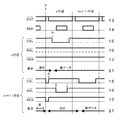
実施形態1の表示装置でn行に新たなデータを書き込む場合、即ち第1の表示信号の替わって第2の表示信号をn行のOLED31に与えて画像を形成する場合には、図2に示すように以下の方法で走査する。この走査において本実施形態では、n行のOLED21の発光の輝度を(n+1)行のOPD31によって検出する。なお、図2は左から右へと走査が進んでいくが、図2の左端では、すでに(n−1)行のOLEDに第2の表示信号であるデータが書き込まれており、n行のOLED21では第1の表示信号の付与による第1の画像が表示される状態が終了し、消灯状態となっている。(n+1)行のOLED21はいまだ前フレームのデータ(第1の表示信号)の表示状態であって、各表示選択線15,15および各検出選択線16,16は非選択状態にある。
When new data is written in n rows in the display device of
〔P〕図2のPで示されたタイミングにおいて、表示データ線13に黒表示電圧(例えば0V)を印加し、かつ(n+1)行の表示選択線15に選択電圧を印加する。同時に、(n+1)行のリセット線17にリセット電圧を印加して、(n+1)行のOPD31の出力電圧をリセットする。この工程によって、(n+1)行のOLED21はしばらく後に消灯(黒表示)となる。
[P] At the timing indicated by P in FIG. 2, a black display voltage (for example, 0 V) is applied to the
〔Q〕Qで示されたタイミングにおいて、(n+1)行の表示選択線15に非選択電圧を印加し、(n+1)行のリセット線17に非リセット電圧を印加する。この工程により、(n+1)行のOLED21を非選択状態に戻す。なお、(n+1)行のOLED21は消灯となっている。
[Q] At the timing indicated by Q, a non-selection voltage is applied to the
〔R〕Rで示されたタイミングにおいて、n行の表示選択線15に選択電圧を印加する。この時、表示データ線13に、これまでの輝度値の検出結果により算出されたn行の補正済み表示データ電圧が印加されている。この工程によって、n行の記憶キャパシタ23にデータが書き込まれn行のOLED21に第2の表示信号が与えられ画像の一部が表示される。
[R] At the timing indicated by R, a selection voltage is applied to the
〔S〕Sで示されたタイミングにおいて、(n+1)行の検出選択線16に選択電圧を印加する。これにより、(n+1)行のOPD31により検出されたn行のOLED21の輝度検出値が検出データ線14に出力される。
[S] At the timing indicated by S, a selection voltage is applied to the
〔T〕Tで示されたタイミングにおいて、(n+1)行の検出選択線16に非選択電圧を印加して、次いで、n行の表示選択線15に非選択電圧を印加する。
[T] At the timing indicated by T, a non-selection voltage is applied to the (n + 1) th row of
以上〔P〕〜〔T〕の工程によって、n行のOLED21に第2の表示信号を与えて表示させ、(n+1)行のOPD31でn行のOLED21の発光の輝度を読み出して、この値を元に補正値を更新する。その後、走査する行を1行ずらして、即ち(n+1)行のOLED21に第2の表示信号を与えて、同様に補正値の更新を行う。このようにして各行を順次走査していく。
Through the steps [P] to [T] described above, the second display signal is given to the n rows of
本実施形態ではn行のOLED21の発光の輝度を(n+1)行のOPD31によって検出しているが、n行と(n+1)行の間の距離は大きくはなく、図5に示すように(n+1)行のOPD31はn行のOLED21に近接する位置に設けられているので、輝度の検出は十分可能である。一方、n行の例えば赤の発光を検出するOPD31では、このOPD31が(n−1)行のOLED21に近接しておりn行のOLED21の発光を検出するタイミングでは(n−1)行のOLED21も画像の一部を表示しているので、(n−1)行の赤いOLED21の発光・消灯によってn行目の赤いOLED21の輝度の検出が、(n+1)行のOPD31によって検出する場合よりも不正確となる。また、例えば(n+1)行の赤の発光を検出するOPD31は、発光しているn行の緑および青のOLED21から遠い位置にあり、かつ緑や青の感度が赤と比べて低いので、緑および青の迷光の影響が小さい。従って、n行の赤の輝度がより正確に検出される。このことは緑および青の輝度検出についても当てはまる。
In this embodiment, the luminance of light emitted from the n rows of
この輝度を検出する走査は、表示装置を使用中、すなわち画像表示中に行うことができる。なお、現実のOLED21の輝度特性は各表示フレーム間では大きく変化しない(低下しない)ことを考慮し、輝度検出を毎フレーム行うことはしないで、何度かのフレームを輝度検出無しで表示した後に行ってもよい。つまり、例えば3フレームに1度のように、輝度検出を行わないフレームを2回表示した後のフレームにおいて輝度検出を行って補正を行ってもよい。輝度検出を行うのは、3フレームに1度に限定されず、2フレームに1度あるいは4フレーム以上に1度でも構わない。輝度検出を行わないフレームが存する場合には消灯期間が短縮できるので、視覚的により高品質な表示が可能となる。
The scanning for detecting the luminance can be performed while the display device is being used, that is, during image display. In consideration of the fact that the luminance characteristic of the
なお、機器始動時における表示初期化は、特許文献2と同様に、
〔1〕全行に対し黒を書き込んだ後、
〔2〕1行目から順次輝線(一つの行のOLED全てが光っているもの)を走査して輝度を検出し、
〔3〕補正値を得る、
という方法で行えばよい。
In addition, the display initialization at the time of apparatus start-up is similar to Patent Document 2,
[1] After writing black on all lines,
[2] The luminance is detected by sequentially scanning the bright lines (all the OLEDs in one row are shining) from the first row,
[3] Obtain a correction value.
You can do this.
本実施形態では、基板上に電気発光素子と光に感応して電気信号を発生する光検出素子との組が複数配置されている表示装置において、表示装置の走査方法を、n行の表示を書き換える際に(n+1)行を消灯し、この消灯期間にn行の表示を書き換えた後の輝度を検出することとした。これによって、n行の輝度補正値をより正確なものとできる。なお、上記(n+1)行の消灯期間は、(n+1)行の表示安定のためのリフレッシュ期間を兼ねている。ここで、リフレッシュ期間とは、表示を新しい内容に書き換えるに当たって、発光素子や駆動トランジスタなどの表示中電圧が印加されつづけたり電流が流れつづけたりする個所の特性を回復させる即ち履歴を消去するために、表示期間と比較して短期間だけ黒表示電圧(0V)や逆電圧を印加する期間のことをさす。直流駆動の場合では、交流駆動の場合と比較して短期的な輝度特性低下が大きいので、リフレッシュ期間を設けるのが好ましい。本実施形態では、リフレッシュ期間と輝度検出のための消灯期間とを兼ねているので、兼ねていない場合に比べて表示の暗線数を低減でき、明度やコントラストの不要な低下を引き起こさないので好ましい。 In the present embodiment, in a display device in which a plurality of sets of electroluminescent elements and light detection elements that generate electric signals in response to light are arranged on a substrate, the scanning method of the display device is changed to display n rows. When rewriting, (n + 1) rows were turned off, and the luminance after rewriting the display of n rows during this turn-off period was detected. As a result, the luminance correction values for n rows can be made more accurate. Note that the turn-off period of the (n + 1) th row also serves as a refresh period for stabilizing the display of the (n + 1) th row. Here, the refresh period is used to restore the characteristics where the display voltage such as the light emitting element and the drive transistor continues to be applied or the current continues to flow when the display is rewritten with new contents, that is, to erase the history. This means a period in which a black display voltage (0 V) or a reverse voltage is applied for a short period of time compared to the display period. In the case of direct current driving, since the short-term luminance characteristic deterioration is larger than in the case of alternating current driving, it is preferable to provide a refresh period. In the present embodiment, since both the refresh period and the extinguishing period for luminance detection are used, the number of dark lines for display can be reduced compared to the case where the refresh period is not used, and it is preferable because it does not cause unnecessary reduction in brightness and contrast.
本実施形態では、電気発光素子と光検出素子との位置関係は、n行の電気発光素子の輝度を(n+1)行の光検出素子で検出している。n行と(n+1)行との間には、一般に表示書き込み行を選択する走査線と輝度読み出し行を選択する走査線とリセット線(リセット線はない場合もあり)とがあるだけなので、輝度検出が十分に可能である。また、輝度を検出したいn行の画素に対して、n行に存在し且つ当該画素隣接する列の電気発光素子の発光の影響は、発光素子の発光スペクトルと光検出素子の吸収スペクトルの重なりが少ないので小さいが、それでも、隣接していると隣の列から入射する迷光の輝度が強すぎて検出値の誤差が大きくなってしまう場合もある。本実施形態では、消灯している(n+1)行の検出素子でn行の電気発光素子の輝度を検出するため、隣の列からの迷光入射の影響を低減できるのでよい。 In the present embodiment, the positional relationship between the electroluminescent elements and the photodetecting elements is that the luminance of the electroluminescent elements in n rows is detected by the photodetecting elements in (n + 1) rows. Since there are generally only a scanning line for selecting a display writing line, a scanning line for selecting a luminance reading line, and a reset line (there may be no reset line) between the n and (n + 1) lines. Detection is sufficiently possible. In addition, for the n rows of pixels for which the luminance is to be detected, the influence of the light emission of the electroluminescent elements in the columns adjacent to the n rows is that the emission spectrum of the light emitting elements and the absorption spectrum of the light detecting elements overlap. However, if it is adjacent, the brightness of the stray light entering from the adjacent column is too strong, and the error of the detection value may increase. In the present embodiment, since the luminance of the electroluminescent elements in the n rows is detected by the (n + 1) rows of detecting elements that are turned off, the influence of stray light incidence from the adjacent columns may be reduced.
本実施形態の表示装置は、基板上に、電気発光素子と光に感応して電気信号を発生する光検出素子との組が複数配置され、光検出素子を構成する層の基板に対する積層順序が、基板上の電気発光素子のうちの少なくともひとつと同じである表示装置とした。なお、光検出素子を構成する複数の層の基板に対する積層順序が、隣接する電気発光素子の少なくともひとつと同じであるのが好ましい。また、光検出素子を構成する複数の層の基板に対する積層順序が、隣接する電気発光素子の少なくともひとつとは異なるのが、さらに好ましい。電気発光素子と光検出素子とをこの構成にして、光検出素子を構成する複数の層の基板に対する積層順序と同じ積層順序の隣接する電気発光素子の輝度を当該光検出素子が主に検出するのが好ましい。光検出素子が、検出したい電気発光素子と同じ材料で作られた構成とすると、電気発光素子の発光スペクトルと類似した光検出素子の吸収スペクトルとなる。カラー表示では、一般に隣接する列の画素は互いに異なる色で構成されているので、電気発光素子の発光スペクトルと光検出素子の吸収スペクトルとの重なりは小さく、隣接する列の発光の光検出素子への影響を低減できる。このように、光検出素子を検出したい電気発光素子と同じ材料で作られた構成とすることで、検出色の選択性を向上でき好ましい。また、作製時に電気発光素子と光検出素子とを同時に積層できるので工程数も低減できて好ましい。 In the display device of this embodiment, a plurality of sets of electroluminescent elements and photodetecting elements that generate electric signals in response to light are arranged on the substrate, and the stacking order of the layers constituting the photodetecting elements with respect to the substrate is The display device is the same as at least one of the electroluminescent elements on the substrate. In addition, it is preferable that the lamination order with respect to the board | substrate of the some layer which comprises a photon detection element is the same as at least one of the adjacent electroluminescent elements. In addition, it is more preferable that the order of stacking a plurality of layers constituting the photodetecting element is different from at least one of the adjacent electroluminescent elements. With this configuration of the electroluminescent element and the photodetecting element, the photodetecting element mainly detects the luminance of the adjacent electroluminescent element in the same stacking order as the stacking order of the plurality of layers constituting the photodetecting element. Is preferred. If the photodetecting element is made of the same material as the electroluminescent element to be detected, the absorption spectrum of the photodetecting element is similar to the emission spectrum of the electroluminescent element. In color display, pixels in adjacent columns are generally composed of different colors, so the overlap between the emission spectrum of the electroluminescent element and the absorption spectrum of the light detecting element is small, and the light emitting element of the adjacent column emits light. Can reduce the effects of As described above, it is preferable that the light detection element is made of the same material as the electroluminescent element to be detected because the selectivity of the detection color can be improved. In addition, since the electroluminescent element and the photodetecting element can be stacked at the same time during manufacturing, the number of processes can be reduced, which is preferable.
本実施形態のOLED21とOPD31との配置は、図5に示される配置であり、これは図4(a)とほぼ同じである。これ以外の配置として、例えば図4(b)、(c)、(d)を例示することができる。図4(a)や(b)に示されている配置は、検出データ線と検出選択線がそれぞれ縦と横に配線されている際に配線が容易になる例である。また、図4(c)、(d)に示されている配置は、検出データ線と検出選択線がそれぞれ縦と横に配線されている場合に、OLEDの面積を小さくして横からの配線をしたりOLED上に横からの配線を敷設したりしなければならないが、図4(a)、(b)の配置に比べて隣の列から入射する迷光の影響を少なくできる例である。
The arrangement of the
本実施形態では図5に示すように、OLED21とOPD31とを一対とする画素を配置しているが、図5は画素配置の一部を例示しているだけで、実際のマトリクスは、例えば、640×480や1280×720などのように縦横とも多くの画素が配置されている。また、図5では赤、緑、青、それぞれでOLED21とOPD31の配置を同じにしたが、同行の赤と青のOPD31が向き合うように配置して迷光の影響をさらに防ぐなどとしてもよい。
In this embodiment, as shown in FIG. 5, a pair of pixels of
(実施形態2)
実施形態2は、図3(b)に示すように、検出部側においてリセットトランジスタ35の代わりに電圧分配抵抗37を1つ設けたことで、リセット線17が不要となりトランジスタが1素子少なくなっていることが実施形態1と異なっており、それ以外は実施形態1と同じであるので、実施形態1と異なっている点を説明する。
(Embodiment 2)
In the second embodiment, as shown in FIG. 3B, by providing one
本実施形態の場合は、実施形態1でのリセットに関する処理を行う必要がないため、画素間のリセット線17や各画素のリセットトランジスタ35が不要になり、これらが形成されていた装置上の領域をOLED21のために利用できる。なお、新たに設けた電圧分配抵抗37は、電源線11と輝度値出力トランジスタ32のゲート電極とを結ぶ配線材の電気抵抗を高くすることで実現可能であるので、面積を増加させずに配置できる。
In the case of the present embodiment, since it is not necessary to perform the process related to the reset in the first embodiment, the
本実施形態では、実施形態1と同様の方法によってOLED21とOPD31などを作製して図3(b)の画素を作り、マトリクス配置する。本実施形態の検出部の回路は、実施形態1の検出部の回路と比較してOLED21の面積を大きくできる反面、輝度検出部に流れる暗電流がわずかに増大してしまう。面積を増大したことによるOLED21の電流密度の減少で得られる寿命向上の効果や視覚的な表示品質などを考慮して、使用する機器にあわせて実施形態1あるいは実施形態2の回路を適宜選択すればよい。
In the present embodiment, the
実施形態2の表示装置は、実施形態1での走査方法からリセット信号の動作を省略して走査することで、実施形態1の表示装置と同様に動作し、実施形態1と同じ効果を奏する。 The display device according to the second embodiment operates in the same manner as the display device according to the first embodiment by performing scanning by omitting the reset signal operation from the scanning method according to the first embodiment, and has the same effects as the first embodiment.
(実施形態3)
実施形態3は、n行の電気発光素子の発光輝度をn行の光検出素子によって検出する点が実施形態1と異なっている点であり、その他の点は実施形態1と同じであるので、実施形態1と異なっている点を説明する。
(Embodiment 3)
The third embodiment is different from the first embodiment in that the light emission luminance of the n rows of electroluminescent elements is detected by the n rows of light detection elements, and the other points are the same as those of the first embodiment. Differences from the first embodiment will be described.
本実施形態では図7に示すように、1つのOLED121と1つのOPD131とを対にして1つの画素としており、OLED121は長方形の一つの角を切り欠いた形状を有しており、その切り欠かれた三角形の部分にOPD131が配置されている。そして、複数の画素を行と列とに並べてマトリクス配置とし、このようにして表示装置を構成している。実施形態1と同じようにOLED121は、データドライバー195から延びる表示データ線113と、走査ドライバー194から延びる表示選択線115とに接続されている。OPD131は、輝度出力回路193から延びる検出データ線114と、走査ドライバー194から延びる検出選択線116およびリセット線117とに接続されている。
In the present embodiment, as shown in FIG. 7, one
任意のn行のOLED121と対になっているn行のOPD131の位置が、実施形態1では(n−1)行のOLEDに隣り合う位置であったのに対し、本実施形態では(n+1)行のOLED121に隣り合う位置となっている点で実施形態1とは異なっている。OPD131の位置をこのようにすることにより、n行のOLED121の発光輝度をn行のOPD131により検出する際に、n行のOPD131は発光している(n−1)行のOLED121からは遠いためこの発光の影響はほとんど受けず、近接している(n+1)行のOLED121は消灯しているのでn行のOPD131の輝度検出に影響を与えない。
The position of the n-row OPD 131 paired with the arbitrary n-
また、画素を構成する回路は、図3(a)に示している実施形態1と同じものでよい。本実施形態の回路は、素子パターンを本実施形態の配置に変更するのみで、実施形態1と同様の手順で作製される。
Further, the circuit constituting the pixel may be the same as that of the first embodiment shown in FIG. The circuit of this embodiment is manufactured in the same procedure as that of
本実施形態におけるn行のOLED121の表示更新は、図6に示す方法によって走査して更新を行う。本実施形態の走査は、実施形態1での走査方法での(n+1)行の検出選択線16と(n+1)行のリセット線17とを、それぞれ、n行の検出選択線116とn行のリセット線117とに変更した点で、実施形態1と異なっている。この走査の差異により、実施形態1では(n+1)行のOPD31でn行のOLED21の輝度を検出し、本実施形態ではn行のOPD131でn行のOLED121の輝度を検出する。n行のOPDがn行のOLEDに対して(n−1)行のOLEDに近いのか(n+1)行のOLEDに近いのかという、OLEDとOPDの相対的な配置によって、実施形態1または本実施形態の走査方法が選択される。なお、本実施形態の効果は実施形態1の効果と同じである。
The display update of the n rows of
(その他の実施形態)
上記の実施形態は本発明の例示であり、本発明はこれらの例に限定されない。
(Other embodiments)
The above embodiments are examples of the present invention, and the present invention is not limited to these examples.
上記実施形態ではOLEDとOPDとをシャドウマスク法を用いて初めから分離したパターンで作製しているが、連続したパターンで作製しておいた後に、例えばレーザー光で一部を加熱し昇華させたり少量の酸素共存下で焼き切ったりして分離パターンを形成してもよい。本発明は、パターンの作製方法に主旨をおくものではないので、実施形態に示していない方法でOLEDおよびOPDをパターニングしても構わない。 In the above embodiment, the OLED and the OPD are manufactured in a pattern that is separated from the beginning using the shadow mask method. The separation pattern may be formed by burning in the presence of a small amount of oxygen. Since the present invention does not focus on the pattern production method, the OLED and OPD may be patterned by a method not shown in the embodiment.
上記実施形態ではリフレッシュ期間に黒表示電圧として0Vを印加したが、電圧印加による特性変化が大きい場合には、より確実な回復をさせるために逆電圧を印加しても構わない。本発明はリフレッシュ方法に主旨をおくものではなく、輝度検出時に消灯していれば、例示した以外のリフレッシュ方法を採用しても構わない。 In the above embodiment, 0 V is applied as the black display voltage during the refresh period. However, when the change in characteristics due to voltage application is large, a reverse voltage may be applied in order to recover more reliably. The present invention does not focus on the refresh method, and a refresh method other than that illustrated may be adopted as long as the light is turned off at the time of luminance detection.
上記実施形態では(n+1)行のOLEDを消灯してからn行のOLEDに表示データを書き込みn行のOLEDの輝度検出をしたが、n行のOLEDに表示データを書き込んでから(n+1)行のOLEDを消灯し次いでn行のOLEDの輝度検出を行っても構わない。 In the above embodiment, the display data is written to the n rows of OLEDs after the (n + 1) rows of OLEDs are turned off, and the luminance of the n rows of OLEDs is detected. However, after the display data is written to the n rows of OLEDs, the (n + 1) rows The OLEDs may be turned off, and then the luminance detection of the n rows of OLEDs may be performed.
また、本発明に用いるOLEDは、一般に知られている材料と積層構造を用いて作製することができる。材料としては、N,N’−ビス(3−メチルフェニル)−N,N’−ビス(フェニル)ベンジジンや1,1−ビス(4−ビス(4−トリル)アミノフェニル)シクロヘキサンやN,N’−ジ(1−ナフチル)−N,N’−ジフェニルベンジジンや銅フタロシアニンやトリス(8−ヒドロキシキノリン)アルミニウムなどが知られている。また、特性向上のために例えば2,9−ジメチル−4,7−ジフェニル−1,10−フェナントロリンや3,4,5−トリフェニル−1,2,4−トリアゾールなどを含む電荷ブロック層や銅フタロシアニンやフッ化リチウムなどを含む注入層、色素をドーパントとして取り込んだ発光層などを設けてもよい。真空蒸着を用いなければ、フルオレン系やチオフェン系などの高分子化合物なども使用できる。そのほかにも、カラーフィルターや乾燥剤など、ダイオード構造の外に他の構成物を備えてもよい。本発明のOLEDは、特定の材料や積層構造に依存するものではない。また、既知の材料や構造のみに限定されるものでないことは、本発明の主旨から明らかである。 In addition, the OLED used in the present invention can be manufactured using a generally known material and a laminated structure. Materials include N, N′-bis (3-methylphenyl) -N, N′-bis (phenyl) benzidine, 1,1-bis (4-bis (4-tolyl) aminophenyl) cyclohexane, N, N '-Di (1-naphthyl) -N, N'-diphenylbenzidine, copper phthalocyanine, tris (8-hydroxyquinoline) aluminum and the like are known. In order to improve the characteristics, for example, a charge blocking layer containing 2,9-dimethyl-4,7-diphenyl-1,10-phenanthroline, 3,4,5-triphenyl-1,2,4-triazole, or copper An injection layer containing phthalocyanine, lithium fluoride, or the like, a light emitting layer in which a dye is incorporated as a dopant, or the like may be provided. If vacuum deposition is not used, a polymer compound such as fluorene or thiophene can be used. In addition, other components such as a color filter and a desiccant may be provided outside the diode structure. The OLED of the present invention does not depend on a specific material or laminated structure. Further, it is apparent from the gist of the present invention that the present invention is not limited to only known materials and structures.
対になっている電気発光素子と光検出素子との配置は図4(a)〜(d)に示されている配置に限定されない。また、電気発光素子と光検出素子との相対的な大きさや形状等も特に限定されない。 The arrangement of the paired electroluminescent element and photodetecting element is not limited to the arrangement shown in FIGS. Further, the relative size and shape of the electroluminescent element and the light detecting element are not particularly limited.
図5、7に示す画素は、カラー表示に対応した赤、緑、青の各画素を同じ形としているが、各色のOLEDの特性によって画素の面積を変え、視覚的に高品質な表示を得るなどの方法をとることも可能である。ある色のOLEDが、本来の特性上低輝度の場合にはその色のOLEDの面積を他の色のOLEDの面積よりも大きくし、逆に、本来の特性上高輝度の場合にはその色のOLEDの面積を他の色のOLEDの面積よりも小さくした設計で、視覚的な色のバランスをとってもよい。 The pixels shown in FIGS. 5 and 7 have the same shape for red, green, and blue pixels corresponding to color display, but the area of the pixel is changed depending on the characteristics of the OLED of each color, and a visually high-quality display is obtained. It is also possible to take a method such as When an OLED of a certain color is low in luminance due to its original characteristics, the area of the OLED of that color is made larger than the area of the OLED of other colors, and conversely, when the OLED is high in luminance due to its original characteristics, the color It is possible to balance the visual color by designing the area of the OLED to be smaller than the areas of the OLEDs of other colors.
本発明の走査ドライバーやデータドライバー、輝度出力回路、輝度補正記録アレイ、補正演算回路は、いずれの実施形態においてもほぼ同様の動作をする。また、実施形態には示していないが、例えば中間階調を出すためのパルス幅変調表示などに対応した回路やフレームサイクル内の表示安定のため駆動トランジスタ部にさらに複雑な回路などを付加してもよい。また、輝度検出回路もより複雑なものとしてもよい。本発明の主旨を逸脱しなければ、これら実施形態の回路に限定されるものではない。 The scan driver, data driver, luminance output circuit, luminance correction recording array, and correction arithmetic circuit of the present invention operate in substantially the same manner in any of the embodiments. Although not shown in the embodiment, for example, a circuit corresponding to a pulse width modulation display for producing an intermediate gradation or a more complicated circuit or the like is added to the drive transistor unit for display stability in the frame cycle. Also good. Further, the luminance detection circuit may be more complicated. Without departing from the gist of the present invention, it is not limited to the circuits of these embodiments.
なお、本願の実施形態は表示パネルのみを示しているが、パネル単独で用いることに限定されるものではない。また、パネルに本実施形態に示されている構成物以外の、例えば乾燥剤などの付加物を設けてもよい。また、基板や封止材、外装材なども適宜変えてもよい。本発明の主旨は、これらの形状、画素数、材質などによって左右されるものではない。 In addition, although embodiment of this application has shown only the display panel, it is not limited to using only a panel. Moreover, you may provide additional materials, such as a desiccant, for example other than the structure shown by this embodiment in a panel. Further, the substrate, the sealing material, the exterior material, and the like may be changed as appropriate. The gist of the present invention does not depend on the shape, the number of pixels, the material, or the like.
以上説明したように、本発明に係る走査方法は、表示を行いながら正確な輝度補正を行うことができ、携帯機器や固定機器の表示部の走査方法等として有用である。 As described above, the scanning method according to the present invention can perform accurate luminance correction while performing display, and is useful as a scanning method for a display unit of a portable device or a fixed device.
11 電源線
12 グランド線
13 表示データ線
14 検出データ線
15 表示選択線
16 検出選択線
17 リセット線
21 OLED
22 駆動トランジスタ
23 記憶キャパシタ
24 データ選択トランジスタ
31 OPD
32 輝度値出力トランジスタ
33 輝度値出力設定抵抗
34 検出選択トランジスタ
35 リセットトランジスタ
36 電圧分配抵抗
37 電圧分配抵抗
91 画素
92 画素アレイ
93 輝度出力回路
94 走査ドライバー
95 データドライバー
96 輝度補正記憶アレイ
97 補正演算回路
112 グランド線
113 表示データ線
114 検出データ線
115 表示選択線
116 検出選択線
117 リセット線
121 OLED
131 OPD
193 輝度出力回路
194 走査ドライバー
195 データドライバー
11
22
32 luminance
131 OPD
193
Claims (5)
前記n行の電気発光素子が、第1の表示信号が与えられて第1の画像の一部を表示するステップAと、
前記ステップAの後に、前記第1の表示信号の付与が停止されるステップBと、
前記ステップBの後に、第2の表示信号が与えられて前記n行の電気発光素子が第2の画像の一部を表示するステップCとを含み、
前記各電気発光素子には光検出素子が近接して設けられており、
前記ステップCでは、(n+1)行の前記電気発光素子が消灯しており、かつn行の前記電気発光素子の発光の輝度を前記光検出素子によって検出する、走査方法。 In a display device in which a plurality of electroluminescent elements are arranged in a plurality of rows on a substrate to form a display surface, a display signal is sequentially applied to the electroluminescent elements for each of the rows, and the display signals are supplied to n rows. A scanning method of forming an image by applying the electroluminescent elements to the (n + 1) rows of the electroluminescent elements,
A step A in which the n rows of electroluminescent elements receive a first display signal and display a portion of a first image;
Step B after application of the first display signal is stopped after Step A;
After step B, a second display signal is provided, and the n rows of electroluminescent elements display a part of the second image, and step C,
Each of the electroluminescent elements is provided with a light detecting element close to the electroluminescent element,
In the step C, the (n + 1) rows of the electroluminescent elements are extinguished and the luminance of light emitted from the n rows of the electroluminescent elements is detected by the photodetecting elements.
Priority Applications (1)
| Application Number | Priority Date | Filing Date | Title |
|---|---|---|---|
| JP2005203630A JP2007024994A (en) | 2005-07-12 | 2005-07-12 | Scanning method |
Applications Claiming Priority (1)
| Application Number | Priority Date | Filing Date | Title |
|---|---|---|---|
| JP2005203630A JP2007024994A (en) | 2005-07-12 | 2005-07-12 | Scanning method |
Related Child Applications (1)
| Application Number | Title | Priority Date | Filing Date |
|---|---|---|---|
| JP2008199501A Division JP5193727B2 (en) | 2008-08-01 | 2008-08-01 | Display device |
Publications (2)
| Publication Number | Publication Date |
|---|---|
| JP2007024994A true JP2007024994A (en) | 2007-02-01 |
| JP2007024994A5 JP2007024994A5 (en) | 2008-08-21 |
Family
ID=37785882
Family Applications (1)
| Application Number | Title | Priority Date | Filing Date |
|---|---|---|---|
| JP2005203630A Withdrawn JP2007024994A (en) | 2005-07-12 | 2005-07-12 | Scanning method |
Country Status (1)
| Country | Link |
|---|---|
| JP (1) | JP2007024994A (en) |
Cited By (4)
| Publication number | Priority date | Publication date | Assignee | Title |
|---|---|---|---|---|
| JP2008216872A (en) * | 2007-03-07 | 2008-09-18 | Hitachi Displays Ltd | Organic el display device |
| JP2010266491A (en) * | 2009-05-12 | 2010-11-25 | Sony Corp | Display apparatus, method for controlling light detection operation |
| CN102507523A (en) * | 2011-11-09 | 2012-06-20 | 大连理工大学 | OLED (Organic Light-Emitting Diode)- and OPD (Organic Photodetector)-based cascading vertical integration capillary electrophoresis chip |
| WO2022144678A1 (en) * | 2020-12-29 | 2022-07-07 | 株式会社半導体エネルギー研究所 | Optical device, display apparatus, and electronic equipment |
-
2005
- 2005-07-12 JP JP2005203630A patent/JP2007024994A/en not_active Withdrawn
Cited By (4)
| Publication number | Priority date | Publication date | Assignee | Title |
|---|---|---|---|---|
| JP2008216872A (en) * | 2007-03-07 | 2008-09-18 | Hitachi Displays Ltd | Organic el display device |
| JP2010266491A (en) * | 2009-05-12 | 2010-11-25 | Sony Corp | Display apparatus, method for controlling light detection operation |
| CN102507523A (en) * | 2011-11-09 | 2012-06-20 | 大连理工大学 | OLED (Organic Light-Emitting Diode)- and OPD (Organic Photodetector)-based cascading vertical integration capillary electrophoresis chip |
| WO2022144678A1 (en) * | 2020-12-29 | 2022-07-07 | 株式会社半導体エネルギー研究所 | Optical device, display apparatus, and electronic equipment |
Similar Documents
| Publication | Publication Date | Title |
|---|---|---|
| CN108649059B (en) | Array substrate, display device and driving method thereof | |
| CN100566483C (en) | Display device and driving method thereof and electronic installation | |
| US9589505B2 (en) | OLED pixel circuit, driving method of the same, and display device | |
| JP5481902B2 (en) | Display panel and display device | |
| US10705648B2 (en) | Pixel circuit, array substrate, display panel, display device and display driving method | |
| US7605792B2 (en) | Driving method and circuit for automatic voltage output of active matrix organic light emitting device and data drive circuit using the same | |
| TW573144B (en) | Self light emitting type display device | |
| US6404137B1 (en) | Display device | |
| JP6192431B2 (en) | Method for driving organic EL display device and organic EL display device | |
| CN108807466A (en) | Display device | |
| US20190121390A1 (en) | Foldable display pannel, display device, image compensation method and image compensation device | |
| US10916614B2 (en) | Array substrate, display panel, light-detecting method therefor and method for controlling the same | |
| JP2014154226A (en) | organic EL display device | |
| JP4816379B2 (en) | Organic electroluminescence device | |
| JP2003173869A (en) | Display device | |
| CN109697954B (en) | Display device and brightness compensation method thereof | |
| JP2010541014A (en) | Pixel circuit | |
| CN110518044B (en) | Display substrate and display device | |
| JP2009500650A (en) | Electroluminescent display device | |
| JP2015225537A (en) | Display device | |
| JP2021512344A (en) | AMOLED display panel with image scanning function | |
| KR20150105706A (en) | Display device | |
| JP2009111047A (en) | Color image display device, shadow mask, and method of manufacturing color image display device using shadow mask | |
| JP2007024994A (en) | Scanning method | |
| JP2010078853A (en) | Matrix display device, and display method of the matrix display device |
Legal Events
| Date | Code | Title | Description |
|---|---|---|---|
| A521 | Request for written amendment filed |
Free format text: JAPANESE INTERMEDIATE CODE: A523 Effective date: 20080702 |
|
| A621 | Written request for application examination |
Free format text: JAPANESE INTERMEDIATE CODE: A621 Effective date: 20080702 |
|
| A761 | Written withdrawal of application |
Free format text: JAPANESE INTERMEDIATE CODE: A761 Effective date: 20100423 |