JP2007018902A - Multicolor light emitting display - Google Patents
Multicolor light emitting display Download PDFInfo
- Publication number
- JP2007018902A JP2007018902A JP2005199857A JP2005199857A JP2007018902A JP 2007018902 A JP2007018902 A JP 2007018902A JP 2005199857 A JP2005199857 A JP 2005199857A JP 2005199857 A JP2005199857 A JP 2005199857A JP 2007018902 A JP2007018902 A JP 2007018902A
- Authority
- JP
- Japan
- Prior art keywords
- green
- blue
- light
- red
- filter
- Prior art date
- Legal status (The legal status is an assumption and is not a legal conclusion. Google has not performed a legal analysis and makes no representation as to the accuracy of the status listed.)
- Pending
Links
Images


Landscapes
- Electroluminescent Light Sources (AREA)
- Optical Filters (AREA)
Abstract
【課題】 4色の光を用いた多色発光表示装置を提供する。
【解決手段】 表示装置11は、行方向m及び列方向nに配列された複数のピクセル20を有する。ピクセル20はそれぞれ、青緑、赤、緑、青色サブピクセル10BG、10R、10G、10Bから成る。赤、緑、青、および青緑色サブピクセル10R、10G、10B、10BGは、それぞれxy色度座標(0.65±0.05,0.35±0.05)、(0.20±0.10,0.70±0.10)、(0.15±0.05,0.06±0.05)、及び、(0.05±0.05,0.60±0.10)の発色光を発する。また青緑色サブピクセル10BGの発光色は、xy色度座標において、xおよびy値が緑色サブピクセル10Gのxおよびy値よりそれぞれ低い。
【選択図】 図1
PROBLEM TO BE SOLVED: To provide a multicolor light emitting display device using four colors of light.
A display device 11 includes a plurality of pixels 20 arranged in a row direction m and a column direction n. Each pixel 20 is composed of blue-green, red, green, and blue sub-pixels 10 BG , 10 R , 10 G , and 10 B. The red, green, blue, and blue-green subpixels 10 R , 10 G , 10 B , and 10 BG have xy chromaticity coordinates (0.65 ± 0.05, 0.35 ± 0.05), (0. 20 ± 0.10, 0.70 ± 0.10), (0.15 ± 0.05, 0.06 ± 0.05), and (0.05 ± 0.05, 0.60 ± 0. 10) The colored light is emitted. In addition, the emission color of the blue-green subpixel 10 BG has lower x and y values than the x and y values of the green subpixel 10 G in the xy chromaticity coordinates.
[Selection] Figure 1
Description
本発明は、4色の光を用いて画像を表示する多色発光表示装置に関する。 The present invention relates to a multicolor light emitting display device that displays an image using four colors of light.
従来、ディスプレイ装置において、フルカラー画像を実現するために、3原色の光を用いることが広く知られている。例えば、有機エレクトロルミネセンス素子(以下、有機EL素子という)を自発光光源として適用したディスプレイにおいては、表示領域上に無数のピクセルが設けられ、各ピクセルそれぞれがR、G、およびBの光を発するサブピクセルから構成される。各サブピクセル(RGB)それぞれは、出力値が調整可能であり、各サブピクセルの出力値それぞれが調整されることにより、各ピクセルは所望の色の光を発することができる。 Conventionally, it is widely known to use light of three primary colors in a display device to realize a full color image. For example, in a display in which an organic electroluminescence element (hereinafter referred to as an organic EL element) is applied as a self-luminous light source, an infinite number of pixels are provided on the display area, and each pixel emits R, G, and B light. Consists of emitting sub-pixels. The output value of each subpixel (RGB) can be adjusted, and each pixel can emit light of a desired color by adjusting the output value of each subpixel.
ここで、各サブピクセルからRGB光を発するためには、例えば特許文献1に記載されるようにRGBカラーフィルタを用いて白色光からRGBの光を抽出する方法が知られている。また、例えば有機EL素子が3色塗り分け方式で製造され、各サブピクセルそれぞれに、赤、緑、青を発する有機EL素子が設けられる方法も知られている。
Here, in order to emit RGB light from each sub-pixel, for example, a method of extracting RGB light from white light using an RGB color filter as described in
ところで、ディスプレイにフルカラー画像を適切に表示するために、カラーテレビにおいては、伝送方式がNTSC方式として規格化されている。NTSC方式においては、伝送される画像の色の再現性を良くするために、RGBそれぞれの色度座標は以下のように規格化されている。
R=(0.64,0.33)
G=(0.21,0.71)
B=(0.15,0.06)
By the way, in order to appropriately display a full-color image on a display, in color television, the transmission method is standardized as the NTSC method. In the NTSC system, chromaticity coordinates of RGB are standardized as follows in order to improve the reproducibility of the color of the transmitted image.
R = (0.64, 0.33)
G = (0.21, 0.71)
B = (0.15, 0.06)
さらに、パーソナルコンピュータのモニター等においては、ネットワーク等でやり取りされる画像等を適切に表示できるように、色の三原色の色度座標はsRGBとして以下のように規格化されている。
R=(0.64,0.33)
G=(0.30,0.60)
B=(0.15,0.06)
Furthermore, in a personal computer monitor or the like, the chromaticity coordinates of the three primary colors are standardized as sRGB as follows so that an image exchanged over a network or the like can be appropriately displayed.
R = (0.64, 0.33)
G = (0.30, 0.60)
B = (0.15, 0.06)
上記規格化されたRGBの色の光が発光できれば、ディスプレイ上においては、上記各RGBのxy座標によって囲まれた領域内の色については、これらRGBを組み合わせることにより表現することができる。
一方、人が生体的に光を感知することができる可視光域は、NTSC方式やsRGBのRGB座標によって囲まれた領域より広く、領域外の色の光についても感知することができる。しかし、このような色については、NTSC方式やsRGB方式においては、ディスプレイ上においては適切に表現することができず、例えば人の眼によって異なる色と感知される色についてもディスプレイ上においては同一の色として表示される場合がある。すなわち、現在のディスプレイにおいては人間が生体的に感知できる色を充分に表現できているとはいえない。 On the other hand, the visible light region in which humans can sense light in a living body is wider than the region surrounded by the NTSC system or RGB coordinates of sRGB, and light outside the region can also be sensed. However, such a color cannot be properly expressed on the display in the NTSC system or the sRGB system. For example, a color that is perceived as a different color depending on human eyes is the same on the display. Sometimes displayed as a color. In other words, it cannot be said that the current display can sufficiently express colors that humans can perceive in a living body.
そこで、本願発明においては、上記問題点に鑑みてなされたものであり、フルカラー画像をより適切に表現することができる表示装置を提供することを目的とする。 Accordingly, the present invention has been made in view of the above problems, and an object thereof is to provide a display device that can more appropriately express a full-color image.
本発明に係る多色発光表示装置は、赤色光を発する赤色サブピクセル、青色光を発する青色サブピクセル、緑色光を発する緑色サブピクセル、及び青と緑色の中間色である青緑色光を発する青緑色サブピクセルを含むピクセルを複数配列して構成され、青緑色サブピクセルの発光色は、xy色度座標において、xおよびy値が緑色サブピクセルのxおよびy値よりそれぞれ低く、かつ赤、緑、青、および青緑色サブピクセルは、それぞれxy色度座標(0.65±0.05,0.35±0.05)、(0.20±0.10,0.70±0.10)、(0.15±0.05,0.06±0.05)、及び(0.05±0.05,0.60±0.10)の発色光を発することを特徴とする。なお、xy色度座標は、CIE(国際照明委員会)1931色度図における色度座標である。 The multicolor light emitting display device according to the present invention includes a red sub-pixel that emits red light, a blue sub-pixel that emits blue light, a green sub-pixel that emits green light, and a blue-green light that emits blue-green light that is an intermediate color between blue and green. The luminescent color of the blue-green sub-pixel is configured such that the x and y values are lower than the x and y values of the green sub-pixel, respectively, and the red, green, The blue and blue-green subpixels are xy chromaticity coordinates (0.65 ± 0.05, 0.35 ± 0.05), (0.20 ± 0.10, 0.70 ± 0.10), It emits colored light of (0.15 ± 0.05, 0.06 ± 0.05) and (0.05 ± 0.05, 0.60 ± 0.10). The xy chromaticity coordinates are chromaticity coordinates in the CIE (International Lighting Commission) 1931 chromaticity diagram.
赤、緑、青、および青緑色サブピクセルは、例えばそれぞれ赤、緑、青、および青緑の光を発する赤、緑、青、および青緑色有機EL素子を含む。 The red, green, blue, and blue-green subpixels include, for example, red, green, blue, and blue-green organic EL elements that emit red, green, blue, and blue-green light, respectively.
赤、緑、青、および青緑色サブピクセルのうち、少なくともいずれかの色のサブピクセルがその色に対応するフィルタを含み、フィルタを含むサブピクセルは、有機EL素子からの光をフィルタで透過させて発色光を得ることが好ましい。本発明においては、有機EL素子とフィルタを組み合わせることにより、各サブピクセルは所望の色度座標を有する光を発することができる。 Among the red, green, blue, and blue-green subpixels, at least one of the color subpixels includes a filter corresponding to the color, and the subpixel including the filter transmits light from the organic EL element through the filter. It is preferable to obtain colored light. In the present invention, by combining an organic EL element and a filter, each subpixel can emit light having a desired chromaticity coordinate.
青、緑、赤、および青緑色サブピクセルは、さらに好ましくはそれぞれ青、緑、赤、および青緑色フィルタを含み、青、緑、赤、および青緑色有機EL素子からの光をそれぞれ青、緑、赤、および青緑色フィルタで透過させて発色光を得る。また、青緑色フィルタは、透過率が最大となる波長が、青色フィルタの透過率が最大となる波長より大きいとともに、緑色フィルタの透過率が最大となる波長より小さいことが好ましい。 The blue, green, red, and blue-green sub-pixels further preferably include blue, green, red, and blue-green filters, respectively, to direct light from blue, green, red, and blue-green organic EL elements to blue, green, respectively , Red and blue-green filters are used to obtain colored light. In the blue-green filter, the wavelength at which the transmittance is maximum is preferably larger than the wavelength at which the transmittance of the blue filter is maximum, and is smaller than the wavelength at which the transmittance of the green filter is maximum.
赤色サブピクセルが赤色フィルタを含む場合、例えば、赤色有機EL素子から発せられる光の発光輝度が最大になる波長が、600〜650nmの範囲のいずれかに位置するとともに、赤色フィルタの透過率が最大になる波長が600nm以上に位置する。緑色サブピクセルが緑色フィルタを含む場合、例えば、緑色有機EL素子から発せられる光の発光輝度が最大になる波長が、510〜550nmの範囲のいずれかに位置するとともに、緑色フィルタの透過率が最大になる波長が510〜550nmの範囲のいずれかに位置する。青色サブピクセルが青色フィルタを含む場合、例えば、青色有機EL素子から発せられる光の発光輝度が最大になる波長が、430〜470nmの範囲のいずれかに位置するとともに、青色フィルタの透過率が最大になる波長が430〜470nmの範囲のいずれかに位置する。このように有機EL素子と、フィルタを適宜組み合わせることにより、赤色、緑色、青色のサブピクセルは、それぞれ色純度が高く所望の色度座標を有する光を発することができる。 When the red sub-pixel includes a red filter, for example, the wavelength at which the emission luminance of light emitted from the red organic EL element is maximized is located in any one of the range of 600 to 650 nm, and the transmittance of the red filter is maximum. The wavelength to be located is 600 nm or more. When the green subpixel includes a green filter, for example, the wavelength at which the emission luminance of light emitted from the green organic EL element is maximized is located in any of the ranges of 510 to 550 nm, and the transmittance of the green filter is maximum. The wavelength to be located is in any of the range of 510 to 550 nm. When the blue subpixel includes a blue filter, for example, the wavelength at which the emission luminance of light emitted from the blue organic EL element is maximized is located in any of the 430 to 470 nm ranges, and the transmittance of the blue filter is maximum. The wavelength to be located is in one of the ranges of 430 to 470 nm. As described above, by appropriately combining the organic EL element and the filter, the red, green, and blue sub-pixels can emit light having high color purity and desired chromaticity coordinates.
青緑色有機EL素子は、例えばその発光層の発光材料としてBAlqが用いられる。この場合、例えば青緑色サブピクセルが青緑色フィルタを含み、青緑色フィルタは、430〜470nmの波長範囲における透過率が20%以下となるとともに、透過率が最大になる波長が490〜510nmに設定され、かつその最大透過率が60%以上に設定される。フィルタがこのように設定されることにより、青緑色有機EL素子の発光層の発光材料としてBAlqを用いた場合、青緑色サブピクセルは色純度の高い青緑色の光を発することができる。 In the blue-green organic EL element, for example, BAlq is used as the light emitting material of the light emitting layer. In this case, for example, the blue-green sub-pixel includes a blue-green filter, and the blue-green filter has a transmittance of 20% or less in the wavelength range of 430 to 470 nm and a wavelength at which the transmittance is maximized is set to 490 to 510 nm. And the maximum transmittance is set to 60% or more. By setting the filter in this way, when BAlq is used as the light emitting material of the light emitting layer of the blue-green organic EL element, the blue-green subpixel can emit blue-green light with high color purity.
本発明に係る液晶ディスプレイ用のバックライトは、一対の透明基板間に配置された液晶層を有する液晶パネルに光を照射する液晶ディスプレイ用のバックライトであって、赤色光を発する赤色サブユニット、青色光を発する青色サブユニット、緑色光を発する緑色サブユニット、及び青と緑色の中間色である青緑色光を発する青緑色サブユニットを含むユニットを複数配列して構成され、青緑色サブユニットの発光色は、xy色度座標において、xおよびy値が緑色サブユニットのxおよびy値よりそれぞれ低く、かつ赤、緑、青、および青緑色サブユニットは、それぞれxy色度座標(0.65±0.05,0.35±0.05)、(0.20±0.10,0.70±0.10)、(0.15±0.05,0.06±0.05)、及び、(0.05±0.05,0.60±0.10)の発色光を発することを特徴とする。 A backlight for a liquid crystal display according to the present invention is a backlight for a liquid crystal display that emits light to a liquid crystal panel having a liquid crystal layer disposed between a pair of transparent substrates, and a red subunit that emits red light. The unit is composed of multiple units including a blue subunit that emits blue light, a green subunit that emits green light, and a blue-green subunit that emits blue-green light, which is an intermediate color between blue and green. The color has x and y values in the xy chromaticity coordinates that are lower than the x and y values of the green subunit, respectively, and the red, green, blue, and turquoise subunits have xy chromaticity coordinates (0.65 ± 0.05, 0.35 ± 0.05), (0.20 ± 0.10, 0.70 ± 0.10), (0.15 ± 0.05, 0.06 ± 0.05), and , (0 Wherein the emitting color light of 05 ± 0.05,0.60 ± 0.10).
本発明によればピクセル内に4つのサブピクセルが設けられ、各サブピクセルそれぞれが赤、緑、青、青緑の光を発することにより、ピクセルは広い色域の光を発することが可能である。したがって、本発明における表示装置は、従来の表示装置に比べ、ディスプレイ上に広範囲な色域によって表現された画像を表示することが可能である。また、本発明に係る液晶ディスプレイ用のバックライトも同様に、ディスプレイ上に広範囲な色域によって表現された画像を表示することが可能である。 According to the present invention, four subpixels are provided in a pixel, and each subpixel emits light of red, green, blue, and blue-green, so that the pixel can emit light of a wide color gamut. . Therefore, the display device according to the present invention can display an image expressed by a wide color gamut on the display as compared with the conventional display device. Similarly, the backlight for a liquid crystal display according to the present invention can display an image expressed in a wide color gamut on the display.
図1は、本発明に係る第1の実施形態における表示装置を示す模式図である。第1の実施形態における表示装置11においては、ピクセル20が、行方向mおよび列方向nにそれぞれ多数配列され、マトリクス状に表示領域を構成している。各ピクセル20は、例えば略正方形に形成され、行方向に4つのサブピクセルがストライプ状に並べられて構成される。ピクセル20を構成する4つのサブピクセルは、図1に示すように、図中左から右に青緑、赤、緑、青色サブピクセル10BG、10R、10G、10Bの順で並べられる。ピクセル20内におけるサブピクセルの配置位置は、すべてのピクセル20において同一である。なお、各サブピクセルは、後述するように自ら発光することにより、表示装置11上に表示される画像の一部を形成する。
FIG. 1 is a schematic diagram showing a display device according to a first embodiment of the present invention. In the
図2は、本実施形態における各ピクセル20の構成を具体的に示す模式図である。各ピクセル20を構成するサブピクセルは、それぞれフィルタおよび有機EL素子によって構成される。各サブピクセル10BG、10R、10G、10Bを構成する青緑、赤、緑、青色有機EL素子23BG、23R、23G、23Bは、それぞれ、青緑、赤、緑、青色の光を発する有機EL素子である。有機EL素子23BG、23R、23G、23Bとともに、各サブピクセル10BG、10R、10G、10Bを構成する青緑、赤、緑、青色フィルタ24BG、24R、24G、24Bは、それぞれ青緑、赤、緑、青の光を透過するフィルタである。
FIG. 2 is a schematic diagram specifically showing the configuration of each
各有機EL素子23BG、23R、23G、23Bは、図2に示すように透明基板30の上面側において、それぞれ青緑色、赤色、緑色、青色有機EL層31BG、31R、31G、31Bが第1電極32(例えば陽極)および第2電極33(例えば陰極)に挟持されて構成される。
As shown in FIG. 2, each organic EL element 23 BG , 23 R , 23 G , 23 B is blue-green, red, green, and blue organic EL layers 31 BG , 31 R , 31 on the upper surface side of the
第1電極32及び第2電極33は、それぞれ互いに平行な複数の第1電極線、第2電極線によって構成され、第1電極線は、第2電極線それぞれに直交するように設けられる。そして、第1電極線と第2電極線とが交叉する位置の間に、それぞれ有機EL層が配置されている。このような構成により、各サブピクセルを構成する有機EL層は、各々独立に電流が入力されるので、各有機EL層の発光輝度は独立に制御される。
The
各フィルタ24BG、24R、24G、24Bは、それぞれ、各有機EL素子23BG、23R、23G、23Bに対応するように、透明基板30の上面に積層される。フィルタ24BG、24R、24G、24Bの上面には、平滑層50が設けられ、平滑層50の上面は平滑化されており、この平滑化された上面に、第1電極(第1電極線)32が被膜される。第1電極32の上面には、各有機EL層31BG、31R、31G、31Bが被膜され、これら有機EL層の上面には、さらに第2電極33が被膜される。
The filters 24 BG , 24 R , 24 G , and 24 B are stacked on the upper surface of the
第1電極(第1電極線)32は、透明電極であって、例えばITO(Indium Tin Oxide)、ATO(Antimony Doped Tindioxide)、ZnO(Zinc Oxide)、IZO(Indium Zinc Oxide)を用いて形成される。また、第2電極(第2電極線)33は例えばアルミニウムを用いて形成されるとともに、平滑層50は、例えばSiO2等を材質として用いて形成される。
The first electrode (first electrode line) 32 is a transparent electrode, and is formed using, for example, ITO (Indium Tin Oxide), ATO (Antimony Doped Tin Dioxide), ZnO (Zinc Oxide), or IZO (Indium Zinc Oxide). The The second electrode (second electrode line) 33 is formed using, for example, aluminum, and the
赤色有機EL層31Rは、例えば陽極側から順に正孔輸送層、赤色発光層、電子輸送層、電子注入層が積層されて構成される。正孔輸送層は、例えば、NPB(N,N’−ジ(ナフタレン−1−イル)―N,N’−ジフェニル−ベンジジン)、TPD(N,N0−ジフェニル−N,N0−ビス(3−メチルフェニル)−1,10−ジフェニル−4,40−ジアミン)等が用いられて形成される。赤色発光層は、例えば緑色発光材料に赤色ドーパント色素がドープされて形成される。緑色発光材料としては、例えばAlq3(トリキノリノレートアルミニウム)等のアルキレート化合物が使用される。赤色ドーパント色素は、特に限定されるわけではないが、DCM2(4−ジシアノメチレン−2−メチル−6−(2−(2,3,6,7−テトラ−ヒドロ−1H,5H−ベンゾ)[ij]キノリジン−8−イル)−4H−ピラン)、DCJTB(4−(ジシアノメチレン)−2−t−ブチル−6−(1,1,7,7−テトラメチルジュロリジル−9−エニル)−4H−ピラン)、ローダミン6G(rhodamine 6G)、DCM(4−(ジシアノメチレン)−2−メチル−6−(p−ジメチルアミノスチリル)−4H−ピラン)等が使用される。電子輸送層は、例えば、緑色発光材料でも使用されるAlq3等のアルキレート化合物が使用される。電子注入層は、例えばAl:Li(アルミリチウム)、またはLiFが用いられて形成される。 The red organic EL layer 31 R is configured by stacking, for example, a hole transport layer, a red light emitting layer, an electron transport layer, and an electron injection layer in order from the anode side. The hole transport layer may be, for example, NPB (N, N′-di (naphthalen-1-yl) -N, N′-diphenyl-benzidine), TPD (N, N0-diphenyl-N, N0-bis (3- Methylphenyl) -1,10-diphenyl-4,40-diamine) or the like. The red light emitting layer is formed, for example, by doping a green light emitting material with a red dopant dye. As the green light emitting material, for example, alkylate compounds such as Alq 3 (triquinolinolate aluminum) are used. The red dopant dye is not particularly limited, but DCM2 (4-dicyanomethylene-2-methyl-6- (2- (2,3,6,7-tetra-hydro-1H, 5H-benzo) [ ij] quinolizin-8-yl) -4H-pyran), DCJTB (4- (dicyanomethylene) -2-tert-butyl-6- (1,1,7,7-tetramethyljulolidyl-9-enyl) -4H-pyran), rhodamine 6G, DCM (4- (dicyanomethylene) -2-methyl-6- (p-dimethylaminostyryl) -4H-pyran) and the like are used. For the electron transport layer, for example, an alkylate compound such as Alq 3 which is also used in a green light emitting material is used. The electron injection layer is formed using, for example, Al: Li (aluminum lithium) or LiF.
緑色有機EL層31Gは、例えば陽極側から順に正孔輸送層、緑色発光層が積層されて構成される。正孔輸送層は、例えば赤色有機EL素子23Rと同様に、NPB、TPD等が用いられて形成される。緑色発光層は、緑色発光材料を用いて形成され、緑色発光材料としては、例えば上述のAlq3等のアルキレート化合物が使用される。 The green organic EL layer 31G is configured by, for example, laminating a hole transport layer and a green light emitting layer in order from the anode side. The hole transport layer is, for example similar to the red organic EL element 23 R, NPB, TPD, and the like are formed is used. The green light emitting layer is formed using a green light emitting material, and as the green light emitting material, for example, an alkylate compound such as Alq 3 described above is used.
青色有機EL層31Bは、例えば陽極側から順に正孔輸送層、青色発光層、電子輸送層が積層されて構成される。正孔輸送層は、例えば赤色有機EL素子23Rと同様に、NPB、TPD等が用いられて形成される。青色発光層は、青色発光材料を用いて形成され、青色発光材料としては、例えばPPCP(1,2,3,4,5−ペンタフェニル−1,3−シクロペンタジエン)のようなシクロペンタジエン系化合物が使用される。また、例えばβ-ADN(9,10−ジ(2−ナフチル)アントラセン)、TBADN(2−t−ブチル−9,10−ジ(2−ナフチル)アントラセン)等のアントラセン誘導体、またはDPVBi(1,4−ビス(2,2−ジフェニルビニル)ビフェニル)、ADS082(4,4−ビス(ジフェニルビニレン)−ビフェニル)等のスチリル誘導体が使用される。なお、青色発光層は、青色発光材料に青色ドーパント色素がドープされても良く、青色ドーパント色素は、例えばペリレン(perylene)や、テトラ(t−ブチル)ペリレン等のペリレン誘導体が使用される。電子輸送層は、例えば、Alq3等のアルキレート化合物が使用される。 The blue organic EL layer 31B is configured by stacking, for example, a hole transport layer, a blue light emitting layer, and an electron transport layer in this order from the anode side. The hole transport layer is, for example similar to the red organic EL element 23 R, NPB, TPD, and the like are formed is used. The blue light-emitting layer is formed using a blue light-emitting material, and examples of the blue light-emitting material include cyclopentadiene compounds such as PPCP (1,2,3,4,5-pentaphenyl-1,3-cyclopentadiene). Is used. In addition, anthracene derivatives such as β-ADN (9,10-di (2-naphthyl) anthracene), TBADN (2-t-butyl-9,10-di (2-naphthyl) anthracene), or DPVBi (1, Styryl derivatives such as 4-bis (2,2-diphenylvinyl) biphenyl) and ADS082 (4,4-bis (diphenylvinylene) -biphenyl) are used. In the blue light emitting layer, a blue light emitting material may be doped with a blue dopant dye. As the blue dopant dye, for example, a perylene derivative such as perylene or tetra (t-butyl) perylene is used. For the electron transport layer, for example, an alkylate compound such as Alq 3 is used.
青緑色有機EL層31BGは、例えば陽極側から順に正孔注入層、正孔輸送層、青緑色発光層、電子注入層が積層されて構成される。正孔注入層は、例えばCuPc(copper phthalocyanine)を用いて形成される。正孔輸送層は、例えば赤色有機EL素子23Rと同様に、NPB、TPD等が用いられて形成される。青緑色発光層は、例えばBAlq(ビス(2メチル−8−キノリノラート)(パラフェニルフェノラート)アルミニウム)が用いられて形成される。また、電子注入層は、例えばAl:Li、またはLiFが用いられて形成される。 The blue-green organic EL layer 31 BG is configured, for example, by laminating a hole injection layer, a hole transport layer, a blue-green light emitting layer, and an electron injection layer in order from the anode side. The hole injection layer is formed using, for example, CuPc (copper phthalocyanine). The hole transport layer is, for example similar to the red organic EL element 23 R, NPB, TPD, and the like are formed is used. The blue-green light emitting layer is formed using, for example, BAlq (bis (2methyl-8-quinolinolato) (paraphenylphenolate) aluminum). The electron injection layer is formed using, for example, Al: Li or LiF.
各フィルタ24BG、24R、24G、24Bは、それぞれ、適宜顔料や染料等が選択されることにより、青緑、赤、緑、青の光を透過するフィルタとして形成される。 Each of the filters 24 BG , 24 R , 24 G , and 24 B is formed as a filter that transmits blue-green, red, green, and blue light by appropriately selecting a pigment, a dye, or the like.
各有機EL素子23BG、23R、23G、23Bは、それぞれ陽極および陰極間に電流が流されると、陽極から正孔が、陰極から電子が注入される。注入された電子と正孔は、青緑色、赤色、緑色、及び青色有機EL層31BG、31R、31G、31Bで、それぞれ再結合し、それぞれの有機EL素子23BG、23R、23G、23Bからそれぞれ青緑色、赤色、緑色、青色の光が出射される。有機EL素子から発せられたそれぞれの光の発光スペクトルの一例を図7に示す。なお、有機EL素子から発せられた光とは、後述する平滑層や透明基板の影響を受けた光をも包含する。有機EL素子から発せられた光は、通常、後述する平滑層及び/又は透明基板などを透過した後、フィルタに入射することになる。しかし、平滑層あるいは透明基板の光透過特性によっては、有機EL素子から発せられた光のスペクトルに影響を及ぼし、有機EL素子そのものから発せられた光のスペクトルとフィルタに入射する光のスペクトルとが一致しなくなる。このようなことを考慮し、本発明では、有機EL素子から発せられた光とは、平滑層や透明基板により、スペクトルに影響を受けた光であってもよい。 In each of the organic EL elements 23 BG , 23 R , 23 G , and 23 B , when current flows between the anode and the cathode, holes are injected from the anode and electrons are injected from the cathode. The injected electrons and holes are recombined in the blue-green, red, green, and blue organic EL layers 31 BG , 31 R , 31 G , and 31 B , respectively, and the respective organic EL elements 23 BG , 23 R , Blue-green, red, green, and blue light is emitted from 23 G and 23 B , respectively. An example of the emission spectrum of each light emitted from the organic EL element is shown in FIG. In addition, the light emitted from the organic EL element includes light affected by a smooth layer and a transparent substrate described later. The light emitted from the organic EL element usually enters a filter after passing through a smoothing layer and / or a transparent substrate described later. However, depending on the light transmission characteristics of the smooth layer or the transparent substrate, it affects the spectrum of light emitted from the organic EL element, and the spectrum of light emitted from the organic EL element itself and the spectrum of light incident on the filter are different. It will not match. In consideration of the above, in the present invention, the light emitted from the organic EL element may be light affected by the spectrum by the smooth layer or the transparent substrate.
各有機EL素子23BG、23R、23G、23Bから出射された青緑色、赤色、緑色、青色の光は、第1電極32及び平滑層50を透過した後、それぞれフィルタ24BG、24R、24G、24Bに入射される。そして、各有機EL素子から発せられた光は、各フィルタ24BG、24R、24G、24Bにおいて、不要な波長の光が適宜取り除かれた後、色純度の高い青緑色、赤色、緑色、青色、の光として透明基板30を透過した後、外部に照射される。すなわち、各サブピクセル10BG、10R、10G、10Bは有機EL素子とフィルタの組み合わせにより、それぞれ色純度の高い青緑、赤、緑、青色の光を発する。そして、これらサブピクセルから発せられた光は混合され、表示装置の1ピクセル、すなわち画像の1ピクセルを構成する。
The blue-green, red, green, and blue light emitted from the organic EL elements 23 BG , 23 R , 23 G , and 23 B passes through the
ここで、赤色サブピクセル10Rから発せられる光のxy色度座標は、(0.65±0.05,0.35±0.05)の範囲内に位置する。青色サブピクセル10Bから発せられる光のxy色度座標は、(0.15±0.05,0.06±0.05)の範囲内に位置する。緑色サブピクセル10Gから発せられる光のxy色度座標は、(0.20±0.10,0.70±0.10)に位置する。そして、青緑色サブピクセル10BGから発せられる光のxy色度座標は、(0.05±0.05,0.60±0.10)の範囲内に位置するとともに、xy色度座標のxおよびy値が緑色サブピクセル10Gのxおよびy値よりそれぞれ低い。 Here, the xy chromaticity coordinates of the light emitted from the red subpixel 10 R are located within the range of (0.65 ± 0.05, 0.35 ± 0.05). The xy chromaticity coordinates of the light emitted from the blue subpixel 10 B are located within the range of (0.15 ± 0.05, 0.06 ± 0.05). The xy chromaticity coordinates of the light emitted from the green subpixel 10 G are located at (0.20 ± 0.10, 0.70 ± 0.10). The xy chromaticity coordinates of light emitted from the blue-green subpixel 10 BG are located within the range of (0.05 ± 0.05, 0.60 ± 0.10), and x of the xy chromaticity coordinates. and y values, respectively below the x and y values of the green sub-pixel 10 G.
これら各サブピクセルの光は、それぞれ有機EL素子に入力される電流値が適宜変更され、各サブピクセルの光の発光強度が調整される。ここで各サブピクセル10BG、10R、10G、10Bは、上記xy色度座標の値の光を発することができるので、各ピクセル20は、各サブピクセルの光の発光強度を調整することにより、上記xy色度座標で囲まれる色度座標の光を発することができる。
With respect to the light of each subpixel, the current value input to the organic EL element is appropriately changed, and the light emission intensity of the light of each subpixel is adjusted. Here, since each subpixel 10 BG , 10 R , 10 G , 10 B can emit light having the value of the xy chromaticity coordinate, each
赤色サブピクセル10Rは、上記xy色度座標の光を得るためには、例えば、赤色サブピクセル10Rから発せられる光の発光輝度が最大になる波長が600〜650nmの範囲内に位置し、発光ピークが1つで、かつそのピークの半値幅が70nm以下に設定される。したがって、赤色有機EL素子23Rは、上記材料が適宜選択されることにより、発する光の発光輝度が最大になる波長λRMAXが、600〜650nmの範囲のいずれかに位置するように設定され、そのピークの半値幅が70nm以下に設定される。また、赤色フィルタ24Rは透過率が最大になる波長が600nm以上に位置し、かつ600nm〜650nmにおける最大透過率が60%以上となるように設定されるとともに、波長域450〜550nmにおいて透過率が15%以下に設定される。このような有機EL素子とフィルタが組み合わされることにより、サブピクセル10Rは、xy色度座標(0.65±0.05,0.35±0.05)の範囲の光を発することが可能となる。なお、本明細書において半値幅とは、いわゆる半値全幅のことであり、極大値の1/2における波の幅をいう。
Red subpixels 10 R, in order to obtain the light of the xy chromaticity coordinates, for example, the wavelength at which the emission luminance is maximized in the light emitted from the red sub-pixel 10 R is positioned within a range of 600 to 650 nm, There is one emission peak, and the half width of the peak is set to 70 nm or less. Therefore, the red organic EL element 23 R is set so that the wavelength λ RMAX at which the emission luminance of the emitted light is maximized is located in any of the ranges of 600 to 650 nm by appropriately selecting the above materials. The half width of the peak is set to 70 nm or less. The red filter 24 R is set so that the wavelength at which the transmittance is maximum is 600 nm or more and the maximum transmittance at 600 nm to 650 nm is 60% or more, and the transmittance is in the
緑色サブピクセル10Gが、上記xy色度座標の光を得るためには、緑色サブピクセル10Gから発せられる光の発光輝度が最大になる波長が例えば510〜550nmの範囲内に位置し、発光ピークが1つで、かつそのピークの半値幅が70nm以下に設定される。したがって、緑色有機EL素子23Gは、上記材料が適宜選択されることにより、発光輝度が最大になる波長λGMAXが、例えば510〜550nmの範囲のいずれかに位置するように設定され、かつそのピークの半値幅が70nm以下に設定されることが好ましい。一方、緑色フィルタ24Gは、例えば透過率が最大になる波長が510〜550nmの範囲に位置するように設定されるとともに、少なくとも波長域510〜550nmにおいて透過率が50%以上になるように設定される。このような有機EL素子とフィルタが組み合わされることにより、サブピクセル10Gは、xy色度座標(0.20±0.10,0.70±0.10)の範囲の光を発することが可能となる。 In order for the green subpixel 10 G to obtain light having the above xy chromaticity coordinates, the wavelength at which the emission luminance of the light emitted from the green subpixel 10 G is maximized is located within a range of 510 to 550 nm, for example. There is one peak, and the half width of the peak is set to 70 nm or less. Therefore, the green organic EL element 23 G is set so that the wavelength λ GMAX at which the light emission luminance is maximized is located in any of the range of, for example, 510 to 550 nm by appropriately selecting the above materials, and It is preferable that the half width of the peak is set to 70 nm or less. On the other hand, for example, the green filter 24 G is set so that the wavelength at which the transmittance is maximum is located in the range of 510 to 550 nm, and the transmittance is set to be 50% or more at least in the wavelength range of 510 to 550 nm. Is done. By combining such an organic EL element and a filter, the subpixel 10 G can emit light in the range of xy chromaticity coordinates (0.20 ± 0.10, 0.70 ± 0.10). It becomes.
青色サブピクセル10Bは、上記xy色度座標の光を得るためには、例えば、青色サブピクセル10Bから発せられる光の発光輝度が最大になる波長が430〜470nmの範囲に位置し、発光ピークが1つで、かつそのピークの半値幅が70nm以下に設定される。したがって、青色有機EL素子23Bは、発光輝度が最大になる波長λBMAXが、430〜470nmの範囲のいずれかに位置するように設定される。また、青色フィルタ24Bは透過率が最大になる波長が430〜470nm内に位置し、かつ波長域430〜470nmにおける透過率が50%以上となるように設定される。また、例えば540nm以上の透過率が20%以下に設定される。このような有機EL素子とフィルタが組み合わされることにより、サブピクセル10Bは、xy色度座標(0.15±0.05,0.06±0.05)の範囲の光を発することが可能となる。 Blue subpixel 10 B, in order to obtain the light of the xy chromaticity coordinates, for example, the wavelength at which the emission luminance is maximized in the light emitted from the blue subpixel 10 B is located in the range of 430 to 470 nm, emission There is one peak, and the half width of the peak is set to 70 nm or less. Therefore, the blue organic EL element 23 B is set so that the wavelength λ BMAX at which the emission luminance is maximized is located in any of the ranges of 430 to 470 nm. The blue filter 24 B is set so that the wavelength at which the transmittance is maximum is located in the range of 430 to 470 nm, and the transmittance in the wavelength region of 430 to 470 nm is 50% or more. For example, the transmittance of 540 nm or more is set to 20% or less. By combining such an organic EL element and a filter, the sub-pixel 10 B can emit light in the range of xy chromaticity coordinates (0.15 ± 0.05, 0.06 ± 0.05). It becomes.
青緑色サブピクセル10BGは、上記xy色度座標の光を得るためには、青緑色サブピクセル10BGから発せられる光はその発光ピークが1つで、発光輝度が最大になる波長が緑色サブピクセル10Gより短く、例えば490〜510nmの範囲に位置しなければならない。ここで、青緑色有機EL素子23BGを上述のように発光層としてBAlqが用いられると、例えば青緑色有機EL素子23BGから発する光は、その発光ピークが2つ見られ、一方のピークは発光輝度が最大になるピークであって、そのピーク波長λBGP1は、450〜470nmの範囲に位置する。また、他方のピークλBGP2は、波長λBGP1の光よりその光の発光輝度は小さく、かつその波長λBGP2が波長λBGP1より長く480〜500nmの範囲に位置する。 In order for the blue-green subpixel 10 BG to obtain light having the above xy chromaticity coordinates, the light emitted from the blue-green subpixel 10 BG has one emission peak, and the wavelength at which the emission luminance is maximized is the green sub-pixel. It must be shorter than the pixel 10 G , for example in the range of 490-510 nm. Here, if BAlq is used a blue-green organic EL element 23 BG as a light-emitting layer as described above, for example, light emitted from the blue-green organic EL element 23 BG, the emission peaks were found two, one peak The peak at which the light emission luminance is maximum, and the peak wavelength λ BGP1 is located in the range of 450 to 470 nm. The other peak lambda BGP2, the light emission luminance than the light of the wavelength lambda BGP1 is small, and the wavelength lambda BGP2 is located in a range of longer 480~500nm than the wavelength lambda BGP1.
このような有機EL素子を用いた場合、青緑色サブピクセル10BGの光の発光輝度が最大になる波長が490〜510nmの範囲に位置するためには、青緑色フィルタ24BGは、一方のピーク波長λBGP1近傍の光を大幅に吸収しなければならない。そこで、本実施形態では、青緑色フィルタ24BGは、少なくとも430〜470nmの波長範囲における透過率が20%以下となるように設定されるとともに、最大透過率の波長が490〜510nmに設定されるとともに、最大透過率は少なくとも60%以上に設定される。また、青緑色フィルタ24BGは、透過率が最大となる波長が、青色フィルタ24Bの透過率が最大となる波長より大きいとともに、緑色フィルタ24Gの透過率が最大となる波長より小さい。このような青緑色フィルタ10BGと青緑色有機EL素子23BGを組み合わせることにより、本実施形態では青緑色サブピクセル10BGは、xy色度座標が(0.05±0.05,0.60±0.10)の光を発するとともに、そのxおよびy値が緑色サブピクセルのxおよびy値よりそれぞれ低い。 When using such an organic EL element, for wavelengths of light emission luminances of the blue-green subpixels 10 BG is maximized is located in the range of 490~510nm, the blue-green filter 24 BG is one of the peak Light near the wavelength λ BGP1 must be absorbed significantly. Therefore, in the present embodiment, the blue-green filter 24 BG is set so that the transmittance in the wavelength range of at least 430 to 470 nm is 20% or less, and the wavelength of the maximum transmittance is set to 490 to 510 nm. At the same time, the maximum transmittance is set to at least 60% or more. Further, blue-green filter 24 BG, the wavelength at which the transmittance becomes maximum, with the wavelength greater than transmittance of the blue filter 24 B is maximum, less than the wavelength at which the transmittance of the green filter 24 G is maximized. By combining such a blue-green filter 10 BG and a blue-green organic EL element 23 BG , in this embodiment, the blue-green subpixel 10 BG has an xy chromaticity coordinate of (0.05 ± 0.05, 0.60). (± 0.10) light and its x and y values are lower than the x and y values of the green subpixel, respectively.
以上説明したように、本実施形態においては、ピクセル20内に4つのサブピクセルが設けられ、各サブピクセルそれぞれが上記xy色度座標に位置する光を発することにより、ピクセル20は広い色域の光を発することが可能である。したがって、本実施形態における表示装置は、従来の表示装置に比べ、ディスプレイ上に広範囲な色域によって表現された画像を表示することが可能である。
As described above, in the present embodiment, four subpixels are provided in the
なお、本実施形態においては、赤、緑、青、および青緑色サブピクセルは、それぞれxy色度座標(0.65,0.35)、(0.20,0.70)、(0.15,0.06)、及び(0.05,0.60)の発色光を発することが好ましい。各サブピクセルが、このようなxy色度座標の光を発することにより、各ピクセルは人が生体的に感度良く感知することができるxy色度座標の色を表示することが可能である。 In the present embodiment, the red, green, blue, and blue-green subpixels have xy chromaticity coordinates (0.65, 0.35), (0.20, 0.70), and (0.15), respectively. , 0.06) and (0.05, 0.60) are preferably emitted. Each sub-pixel emits light having such an xy chromaticity coordinate, so that each pixel can display a color having an xy chromaticity coordinate that can be sensed by humans with high sensitivity.
さらに、ピクセル20内におけるサブピクセルは、図1のようにストライプ状に配置される場合に限らず、例えば図3に示すように配置されても良い。すなわち、サブピクセル1010R、10G、10BG、10Bはそれぞれ略正方形に形成され、行方向mに2つ、列方向nに2つの4つのサブピクセルによって1つのピクセル20が構成されていても良い。ピクセル20を構成する4つのサブピクセル10は、図3に示すようにそれぞれサブピクセル10R、10G、10BG、10Bであって、ピクセル20内において、サブピクセル10G、10BGが対角の位置に配置されている。なお、ピクセル20内におけるサブピクセル10の配置位置は、すべてのピクセル20において同一である。
Further, the sub-pixels in the
次に、第2の実施形態について説明する。第1の実施形態に係る表示装置においては、有機EL素子は、自発光光源として利用されたが、第2の実施形態においては、有機EL素子が液晶ディスプレイのバックライトに利用される。 Next, a second embodiment will be described. In the display device according to the first embodiment, the organic EL element is used as a self-luminous light source. In the second embodiment, the organic EL element is used as a backlight of a liquid crystal display.
図4は、本実施形態に係る液晶ディスプレイを模式的に示した斜視図である。図4に示すように、液晶ディスプレイ210は、バックライト220と、液晶パネル100を備える。
FIG. 4 is a perspective view schematically showing the liquid crystal display according to the present embodiment. As shown in FIG. 4, the
液晶パネル100は、図中下方側に設けられた第1基板101、図中上方側に設けられた第2基板102の間に、下方側から順に、液晶用カラーフィルタ103、第1液晶用電極部104、液晶層110、第2液晶用電極部105が配置されて構成される。第1基板101の図中下面側には、第1偏光フィルタ111が、第2基板102の上面側には第2偏光フィルタ112が設けられる。第1及び第2基板101、102は、透明基板であって、プラスチック、ガラス基板等から成る。
The
第1及び第2液晶用電極部104、105は、透明電極であって、それぞれ互いに平行な複数の第1電極線104a、第2電極線105bによって構成され、各第1電極線104aは、各第2電極線105bに直交するように設けられる。そして、第1電極線104aと第2電極線105bとが交叉する位置それぞれにおいて、第1電極線104aおよび第2電極線105bの間に積層される液晶層110の各部分は、1画素Pを構成する。液晶層110の各画素Pは、第1電極線104a及び第2電極線105bから印加される電圧により、分子の配列状態が変化させられる。
The first and second liquid
液晶用カラーフィルタ103は、液晶用赤色フィルタ103R、液晶用緑色フィルタ103G、及び液晶用青色フィルタ103Bがストライプ状に並べられて構成される。各液晶用フィルタ103R、103G、103Bは、その幅が1画素の幅に対応するように形成され、それぞれ第1電極線104aに沿うように延びる。
The liquid
図5は、バックライト220の断面図である。以下、図4及び図5を用いてバックライトの構成について説明する。バックライト220は、図4に示すように透明基板230に複数のELユニット221が設けられて構成される。
FIG. 5 is a cross-sectional view of the
各ELユニット221は、図5に示すように青緑、赤、緑、青色ELサブユニット222BG、222R、222G、222Bから成る。各ELサブユニット222BG、222R、222G、222Bは、それぞれ青緑色、赤色、緑色、青色有機EL素子223BG、223R、223G、223B及び青緑、赤、緑、青色フィルタ224BG、224R、224G、224Bが組み合わされて構成される。
Each
各フィルタ224BG、224R、224G、224Bは、それぞれ、各有機EL素子223BG、223R、223G、223Bに対応するように、透明基板230の上面に積層される。フィルタ224BG、224R、224G、224Bの上面には、第1の実施形態と同様に、平滑層250が設けられ、平滑層250の上面は平滑化されており、この平滑化された上面に、第1電極(第1電極線)232が被膜される。
Each filter 224 BG, 224 R, 224 G , 224 B , respectively, each of the organic EL element 223 BG, 223 R, 223 G , 223 so as to correspond to B, are stacked on the upper surface of the
各有機EL素子223BG、223R、223G、223Bは、図5に示すようにそれぞれ第1電極232(例えば陽極)上に積層され、それぞれの青緑色、赤色、緑色、青色有機EL層231BG、231R、231G、231Bは、第1電極232(例えば陽極)および第2電極233(例えば陰極)に挟持されて構成される。
Each organic EL element 223 BG, 223 R, 223 G , 223 B are stacked on the
なお、ELユニット221を構成する有機EL層231BG、231R、231G、231Bは、第1の実施形態と同様に、ELユニット221内においてストライプ状に並べられている。そして、ELユニット221についても、第1の実施形態と同様に行方向m、列方向nに無数に並べられている。ELユニット221内における各有機EL層の配置位置は、すべてのユニット221において同一であっても良いし、異なっていても良い。また、図3に示すように、ELユニット221は、行方向mに2つ、列方向nに2つ並べられた4つのサブユニットによって1つのELユニット221が構成されていても良い。
Note that the organic EL layers 231 BG , 231 R , 231 G , and 231 B constituting the
各有機EL層231BG、231R、231G、231Bの第1電極232上における占有面積は、それぞれ液晶層110の1画素P分の面積よりも大きく、例えばELユニット221の第1電極232上における占有面積は少なくとも液晶層110の4画素分以上の面積を占める。
The occupied area of each organic EL layer 231 BG , 231 R , 231 G , 231 B on the
なお、各有機EL層231BG、231R、231G、231B、第1電極及び第2電極232、233、及びフィルタ224BG、224R、224G、224Bの構成は、第1の実施形態と同様であるのでその記載は省略する。ただし、第1の実施形態における第1及び第2電極32、33は、それぞれ複数の電極線に分割されていたが、第2の実施形態に係る第1及び第2電極232、233は、複数の電極線に分割されずに単一電極であっても良い。第2の実施形態において有機EL素子は、バックライトに用いられるので、ELサブユニット(及びELユニット)毎に電流のオン−オフ、及び電流量が調整される必要がないからである。
The configurations of the organic EL layers 231 BG , 231 R , 231 G , 231 B , first and
以下、本実施形態に係る液晶パネルの動作について、図4、5を参照しつつ説明する。第1及び第2電極232及び233間に電流が流され、各有機EL層231BG、231R、231G、231Bに正孔と電子が注入されると、各EL層で電子と正孔が再結合され、各有機EL層231BG、231R、231G、231Bからは青緑色、赤色、緑色、青色の光が出射される。出射された光は、第1電極232及び平滑層250を介して、それぞれフィルタ224BG、224R、224G、224Bに入射される。そして、各カラーフィルタ224BG、224R、224G、224Bにおいて、不要な波長の光が適宜取り除かれた後、色純度の高い青緑色、赤色、緑色、青色、の光として透明基板を透過して外部に出射される。すなわち、各ELサブユニット222BG、222R、222G、222Bは、色純度の高い青緑色、赤色、緑色、青色、の光を外部に出射する。
Hereinafter, the operation of the liquid crystal panel according to the present embodiment will be described with reference to FIGS. When a current flows between the first and
各ELサブユニット222BG、222R、222G、222Bから出射された光は、拡散光であり、青緑色、赤色、緑色、青色の光は、混合され、白色光として液晶パネル100に入射される。液晶パネル100に入射された白色光は、第2偏光フィルタ112及び第2基板102を透過して、偏光として液晶層110に導入される。導入された偏光は、画素P毎に分子の配列状態の異なる液晶層110で変調させられ所定の偏光となった後、液晶用カラーフィルタ103によって赤、緑、青色のいずれかの光となる。これら赤、緑、青色の光は、第1基板101を通過した後、第1偏光フィルタ111で透過または吸収される。第1偏光フィルタ111を透過した光は、外部に出射され、画像を形成する。
Light emitted from each of the EL subunits 222 BG , 222 R , 222 G , and 222 B is diffused light, and blue-green, red, green, and blue light are mixed and incident on the
各有機EL層231R、231G、231BG、231Bから発せられる光は、上記xy色度座標を有する光であって、これらの光が混合されて得られた光は、上述したように色域が非常に広い。したがって、本実施形態における液晶ディスプレイ210は、色再現性の良い画像を表示することができる。また、本実施形態においては、液晶用カラーフィルタ103は3色しか設けられなかったが、バックライト220と同様に、赤色、緑色及び青色フィルタに加えて、青緑色フィルタが設けられても良い。
The light emitted from each organic EL layer 231 R , 231 G , 231 BG , 231 B is light having the xy chromaticity coordinates, and the light obtained by mixing these lights is as described above. The color gamut is very wide. Therefore, the
なお、第1及び第2の実施形態においては、各サブピクセル及び各ELサブユニットが、有機EL素子とフィルタの組み合わせにより構成されているが、有機EL素子の色純度が高い場合、フィルタを省略しても良い。また、場合によって、特定の色のサブピクセルに関し、フィルタを省略しても良い。 In the first and second embodiments, each subpixel and each EL subunit are configured by a combination of an organic EL element and a filter. However, when the color purity of the organic EL element is high, the filter is omitted. You may do it. In some cases, the filter may be omitted for a specific color sub-pixel.
なお、第1の実施形態においては、各フィルタ24BG、24R、24G、24Bは電極と基板の間に配置されたが、図6に示すように、透明基板30の下面側に配置されても良い。ただし、各フィルタ24BG、24R、24G、24Bは本実施形態と同様に、それぞれの有機EL素子23BG、23R、23G、23Bに対応するように設けられる。さらに、図6においては、平滑層は設けられず、第1電極32が透明基板30に直接積層される。また、第2の実施形態においても、同様にフィルタ224BG、224R、224G、224Bは、透明基板の下面側に設けられても良い。
In the first embodiment, the filters 24 BG , 24 R , 24 G , and 24 B are disposed between the electrodes and the substrate, but are disposed on the lower surface side of the
以下、本発明について、実施例を用いてさらに詳細に説明するが、本発明は以下に述べる実施例に限定されるわけではない。なお、実施例においては、各色の有機EL素子とカラーフィルタを組み合わせたときの各発光色のxy色度座標を確認した。 EXAMPLES Hereinafter, although this invention is demonstrated further in detail using an Example, this invention is not necessarily limited to the Example described below. In the examples, the xy chromaticity coordinates of the respective emission colors when the organic EL elements of the respective colors and the color filters were combined were confirmed.
(1)赤色
(A)有機EL素子
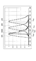
まず、ガラスから成る透明基板上に、赤色フィルタを設け、その赤色フィルタの上にSiO2から成る平滑層を積層した。そして、この平滑層の上に、ITOから成る透明電極(陽極)、NPBから成る正孔輸送層を、この順に真空蒸着により積層した後、その上にDCJTBを緑色発光材料Alq3にドープした赤色発光層を積層した。赤色発光層は、緑色発光材料であるAlq3に赤色ドーパント色素であるDCJTBを同時に真空蒸着し形成した。このとき、DCJTBはAlq3に対して1重量%ドープした。赤色発光層の上に、Alq3から成る電子輸送層、LiFから成る電子注入層、アルミニウムから成る陰極を順に、真空蒸着により積層し、赤色有機EL素子を得た。なお、各層の厚さは、透明基板が0.7mm、平滑層が400nm、陽極が125nm、正孔輸送層が60nm、赤色発光層が40nm、電子輸送層が40nm、電子注入層が5nm、陰極が100nmであった。有機EL素子から、発せられる光の発光スペクトルは図7に示す。なお、図7において、横軸は波長(nm)、縦軸は発光輝度を表し、発光輝度は各有機EL素子における最大値を1として表した。
(1) Red (A) Organic EL Element First, a red filter was provided on a transparent substrate made of glass, and a smooth layer made of SiO 2 was laminated on the red filter. On this smooth layer, a transparent electrode (anode) made of ITO and a hole transport layer made of NPB were laminated in this order by vacuum deposition, and then DCJTB was doped with green light emitting material Alq 3 on the red color. A light emitting layer was laminated. The red light-emitting layer was formed by simultaneously vacuum depositing DCJTB, which is a red dopant dye, on Alq 3 , which is a green light-emitting material. At this time, DCJTB was 1 wt% doped into the Alq 3. On the red light emitting layer, an electron transport layer made of Alq 3 , an electron injection layer made of LiF, and a cathode made of aluminum were sequentially laminated by vacuum deposition to obtain a red organic EL device. The thickness of each layer is 0.7 mm for the transparent substrate, 400 nm for the smooth layer, 125 nm for the anode, 60 nm for the hole transport layer, 40 nm for the red light emitting layer, 40 nm for the electron transport layer, 5 nm for the electron injection layer, It was 100 nm. An emission spectrum of light emitted from the organic EL element is shown in FIG. In FIG. 7, the horizontal axis represents wavelength (nm), the vertical axis represents light emission luminance, and the light emission luminance is represented by 1 as the maximum value in each organic EL element.
図7に示すように、赤色有機EL素子から発せられる光は、発光ピークが1つから成り、発光輝度が最大になる波長λRMAXは620nmであった。また発光輝度の最大値を1としたとき、590〜650nmにおいて、発光輝度が1/2以上となり、すなわち発光ピークの半値幅は60nmであった。 As shown in FIG. 7, the light emitted from the red organic EL element has one emission peak, and the wavelength λ RMAX at which the emission luminance is maximized was 620 nm. When the maximum value of the light emission luminance was 1, the light emission luminance was ½ or more at 590 to 650 nm, that is, the half width of the light emission peak was 60 nm.
(B)カラーフィルタ
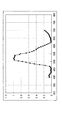
赤色フィルタは、Lee Filter社製の182 Light Red(商品名)を用いた。このフィルタの分光特性を図8に示す。図8中、横軸は波長(nm)、縦軸は透過率(×100%)を表す。図8に示すように、赤色フィルタにおいては、585〜700nmにおいて、透過率が50%以上になるとともに、600〜700nmにおいて、透過率が80%以上と成った。また、透過率は645nmで最大となった。一方、波長域450〜550nmにおいて透過率は10%以下であった。
(B) Color filter 182 Light Red (trade name) manufactured by Lee Filter was used as the red filter. The spectral characteristics of this filter are shown in FIG. In FIG. 8, the horizontal axis represents wavelength (nm) and the vertical axis represents transmittance (× 100%). As shown in FIG. 8, in the red filter, the transmittance was 50% or more at 585 to 700 nm, and the transmittance was 80% or more at 600 to 700 nm. Further, the transmittance reached a maximum at 645 nm. On the other hand, the transmittance was 10% or less in the wavelength region of 450 to 550 nm.
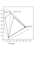
上記有機EL素子と、カラーフィルタを組み合わせ、有機EL素子からの光をカラーフィルタ及び透明基板を介して取り出したときの光の色度座標xyを図12に示す。図12においては横軸をX、縦軸をYとする。図12に示すように赤色光の色度座標xyは(0.66,0.34)であった。なお、図12においては、参考のためにNTSC方式において規格化されているRGBの値、及びsRGBにおいて規格化されているRGBの値についてもそれぞれ点線及び一点鎖線で示す。また、本実施例においては、平滑層及び透明基板は、入射する光に対してスペクトルを変化させないフラットな透過特性を有するものを使用した。 FIG. 12 shows chromaticity coordinates xy of light when the organic EL element is combined with a color filter and light from the organic EL element is extracted through the color filter and the transparent substrate. In FIG. 12, the horizontal axis is X and the vertical axis is Y. As shown in FIG. 12, the chromaticity coordinate xy of red light was (0.66, 0.34). In FIG. 12, for reference, RGB values standardized in the NTSC system and RGB values standardized in sRGB are also indicated by dotted lines and alternate long and short dash lines, respectively. In this embodiment, the smooth layer and the transparent substrate have flat transmission characteristics that do not change the spectrum with respect to incident light.
(2)緑色
(A)有機EL素子
まず、ガラスから成る透明基板上に、緑色フィルタを設け、その緑色フィルタの上にSiO2から成る平滑層を積層した。そして、平滑層の上にITOから成る透明電極(陽極)、NPBから成る正孔輸送層、Alq3から成る緑色発光層、アルミニウムから成る陰極をこの順に、真空蒸着により積層し、緑色有機EL素子を得た。なお、各層の厚さは、透明基板0.7mm、平滑層400nm、陽極が125nm、正孔輸送層が40nm、緑色発光層が40nm、陰極が100nmであった。有機EL素子から発せられる光の発光スペクトルは図7に示す。
(2) Green (A) Organic EL Element First, a green filter was provided on a transparent substrate made of glass, and a smooth layer made of SiO 2 was laminated on the green filter. Then, a transparent electrode (anode) made of ITO, a hole transport layer made of NPB, a green light emitting layer made of Alq 3 and a cathode made of aluminum are laminated in this order on the smooth layer by vacuum deposition, thereby producing a green organic EL element. Got. The thickness of each layer was 0.7 mm for the transparent substrate, 400 nm for the smooth layer, 125 nm for the anode, 40 nm for the hole transport layer, 40 nm for the green light emitting layer, and 100 nm for the cathode. An emission spectrum of light emitted from the organic EL element is shown in FIG.
図7に示すように、緑色有機EL素子から発せられる光は、発光ピークが1つから成り、発光輝度が最大になる波長λGMAXは530nmであった。また発光輝度の最大値を1としたとき、500〜565nmにおいて、発光輝度が1/2以上となり、すなわちこのピークの半値幅は65nmであった。 As shown in FIG. 7, the light emitted from the green organic EL element has one emission peak, and the wavelength λ GMAX at which the emission luminance is maximum was 530 nm. When the maximum value of the light emission luminance was 1, the light emission luminance was ½ or more at 500 to 565 nm, that is, the half width of this peak was 65 nm.
(B)カラーフィルタ
緑色フィルタは、Lee Filter社製の122 Fern Green(商品名)を用いた。このフィルタの分光特性を図9に示す。図9中、横軸は波長(nm)、縦軸は透過率(×100%)を表す。図9に示すように、緑色フィルタにおいては、520nmにおいて透過率が最大になるとともに、500〜550nmにおいて透過率が70%以上になった。また、490〜565nmにおいて、透過率が最大透過率の1/2以上となり、すなわち半値幅が75nmであった。
(B) Color filter 122 Fern Green (trade name) manufactured by Lee Filter was used as the green filter. The spectral characteristics of this filter are shown in FIG. In FIG. 9, the horizontal axis represents wavelength (nm) and the vertical axis represents transmittance (× 100%). As shown in FIG. 9, in the green filter, the transmittance was maximum at 520 nm, and the transmittance was 70% or more at 500 to 550 nm. Moreover, in 490-565 nm, the transmittance | permeability became 1/2 or more of the maximum transmittance, ie, the half value width was 75 nm.
上記有機EL素子と、カラーフィルタを組み合わせ、有機EL素子からの光を、上記カラーフィルタ及び透明基板を介して取り出した場合、光の色度座標xyは(0.21,0.70)であった(図12参照)。 When the organic EL element and the color filter are combined and light from the organic EL element is extracted through the color filter and the transparent substrate, the chromaticity coordinate xy of the light is (0.21, 0.70). (See FIG. 12).
(3)青色
(A)有機EL素子
まず、ガラスから成る透明基板上に、青色フィルタを設け、その青色フィルタの上にSiO2から成る平滑層を積層した。そして平滑層の上にITOから成る透明電極(陽極)、TPDから成る正孔輸送層、PPCPから成る青色発光層、Alq3から成る電子輸送層、アルミニウムから成る陰極をこの順に、真空蒸着により積層し、青色有機EL素子を得た。なお、各層の厚さは、透明基板が0.7mm、平滑層が400nm、陽極が125nm、正孔輸送層が40nm、青色発光層が30nm、電子輸送層が30nm、陰極が100nmであった。有機EL素子から発せられる光の発光スペクトルは図7に示す。
(3) Blue (A) Organic EL Element First, a blue filter was provided on a transparent substrate made of glass, and a smooth layer made of SiO 2 was laminated on the blue filter. A transparent electrode (anode) made of ITO, a hole transport layer made of TPD, a blue light emitting layer made of PPCP, an electron transport layer made of Alq 3 and a cathode made of aluminum were laminated in this order on the smooth layer by vacuum deposition. As a result, a blue organic EL device was obtained. The thickness of each layer was 0.7 mm for the transparent substrate, 400 nm for the smooth layer, 125 nm for the anode, 40 nm for the hole transport layer, 30 nm for the blue light emitting layer, 30 nm for the electron transport layer, and 100 nm for the cathode. An emission spectrum of light emitted from the organic EL element is shown in FIG.
図7に示すように、青色有機EL素子から発せられる光は、発光ピークが1つから成り、発光輝度が最大になる波長λBMAXは445nmであった。また発光輝度の最大値を1としたとき、415〜475nmにおいて、発光輝度が1/2以上となり、すなわちピークの半値幅は60nmであった。 As shown in FIG. 7, the light emitted from the blue organic EL element has one emission peak, and the wavelength λ BMAX at which the emission luminance is maximized was 445 nm. When the maximum value of the light emission luminance was 1, the light emission luminance was ½ or more at 415 to 475 nm, that is, the half width of the peak was 60 nm.
(B)カラーフィルタ
青色フィルタは、Lee Filter社製の183 Moonlight Blue(商品名)を用いた。このフィルタの分光特性を図10に示す。図10中、横軸は波長(nm)、縦軸は透過率(×100%)を表す。図10に示すように、青色フィルタにおいては、470nmにおいてその透過率が最大となるとともに、435〜495nmにおいて透過率が70%以上になった。また、405〜515nmにおいて透過率が50%以上になるとともに、540nm以上の透過率が20%以下であった。
(B) Color filter The blue filter used was 183 Moonlight Blue (trade name) manufactured by Lee Filter. The spectral characteristics of this filter are shown in FIG. In FIG. 10, the horizontal axis represents wavelength (nm) and the vertical axis represents transmittance (× 100%). As shown in FIG. 10, in the blue filter, the transmittance was maximum at 470 nm, and the transmittance was 70% or more at 435 to 495 nm. Further, the transmittance at 405 to 515 nm was 50% or more, and the transmittance at 540 nm or more was 20% or less.
上記有機EL素子と、カラーフィルタを組み合わせ、有機EL素子からの光をカラーフィルタ及び透明基板を介して取り出したときの光の色度座標xyは(0.15,0.05)であった(図12参照)。 When the organic EL element and the color filter are combined, and the light from the organic EL element is taken out through the color filter and the transparent substrate, the chromaticity coordinate xy of the light is (0.15, 0.05) ( (See FIG. 12).
(4)青緑色
(A)有機EL素子
まず、ガラスから成る透明基板上に、青緑色フィルタを設け、その青緑色フィルタの上にSiO2から成る平滑層を積層した。そして、平滑層の上に、透明基板上にITOから成る透明電極(陽極)、CuPcから成る正孔注入層、NPBから成る正孔輸送層、BAlqから成る青緑色発光層、LiFから成る電子注入層、アルミニウムから成る陰極を、この順に真空蒸着により、積層し、青緑色有機EL素子を得た。なお、各層の厚さは、透明基板が0.7mm、平滑層が400nm、陽極が125nm、正孔注入層が10nm、正孔輸送層が30nm、青緑色発光層が40nm、電子注入層が5nm、陰極が100nmであった。青緑色有機EL素子から発せられる光の発光スペクトルは図7に示す。
(4) Blue-green (A) organic EL element First, a blue-green filter was provided on a transparent substrate made of glass, and a smooth layer made of SiO 2 was laminated on the blue-green filter. And on the smooth layer, transparent electrode (anode) made of ITO on the transparent substrate, hole injection layer made of CuPc, hole transport layer made of NPB, blue-green light emitting layer made of BAlq, electron injection made of LiF A cathode composed of layers and aluminum was laminated in this order by vacuum vapor deposition to obtain a blue-green organic EL element. The thickness of each layer is 0.7 mm for the transparent substrate, 400 nm for the smooth layer, 125 nm for the anode, 10 nm for the hole injection layer, 30 nm for the hole transport layer, 40 nm for the blue-green light emitting layer, 5 nm for the electron injection layer, The cathode was 100 nm. An emission spectrum of light emitted from the blue-green organic EL element is shown in FIG.
図7に示すように、青緑色有機EL素子から発せられる光は、その発光ピークが2つ見られ、一方のピークは発光輝度が最大になるピークであって、そのピーク波長λBGP1は460nmであった。他方のピークは、その発光輝度が一方のピークの発光輝度を1とすると、0.47であり、その波長λBGP2が490nmであった。 As shown in FIG. 7, the light emitted from the blue-green organic EL element has two emission peaks, one peak is a peak at which the emission luminance is maximum, and the peak wavelength λ BGP1 is 460 nm. there were. The other peak had a light emission luminance of 0.47, where the light emission luminance of one peak was 1, and its wavelength λ BGP2 was 490 nm.
(B)カラーフィルタ
青緑色フィルタは、Lee Filter社製の124 Dark Green(商品名)を用いた。このフィルタの分光特性を図11に示す。図11に示すように、青緑色フィルタにおいては、透過率が最大になる波長が505nmであった。このフィルタにおいては、495〜535nmにおいては、その透過率が80%以上であるとともに、430〜485nmにおいては、透過率が10%以下に抑えられていた。
(B) Color filter 124 Dark Green (trade name) manufactured by Lee Filter was used as the blue-green filter. The spectral characteristics of this filter are shown in FIG. As shown in FIG. 11, in the blue-green filter, the wavelength at which the transmittance is maximum is 505 nm. In this filter, the transmittance at 495 to 535 nm is 80% or more, and at 430 to 485 nm, the transmittance is suppressed to 10% or less.
上記有機EL素子と、カラーフィルタを組み合わせ、有機EL素子からの光を、上記カラーフィルタ及び透明基板を介して取り出した場合、光の色度座標xyは(0.05,0.59)であった(図12参照)。 When the organic EL element and the color filter are combined and light from the organic EL element is extracted through the color filter and the transparent substrate, the chromaticity coordinate xy of the light is (0.05, 0.59). (See FIG. 12).
以上実施例から、上述した有機EL素子と、カラーフィルタを組み合わせることにより、4つのサブピクセル(又はサブユニット)が、(0.05,0.59)、(0.66,0.34)、(0.21,0.70)、及び(0.15,0.05)の光を発することができることが理解できる。すなわち、実施例に係る表示装置(又は液晶ディスプレイ用のバックライト)は、これら有機EL素子とカラーフィルタが組み合わされることにより、上記xy色度座標で囲まれる色を、表現可能である。 From the embodiments described above, by combining the organic EL element and the color filter described above, four subpixels (or subunits) are (0.05, 0.59), (0.66, 0.34), It can be understood that light of (0.21, 0.70) and (0.15, 0.05) can be emitted. That is, the display device according to the embodiment (or the backlight for the liquid crystal display) can express the color surrounded by the xy chromaticity coordinates by combining the organic EL element and the color filter.
10BG 青緑色サブピクセル
10R 赤色サブピクセル
10G 緑色サブピクセル
10B 青色サブピクセル
20 ピクセル
23BG、223BG 青緑色有機EL素子
23R、223R 赤色有機EL素子
23G、223G 緑色有機EL素子
23B、223B 青色有機EL素子
24BG、224BG 青緑色フィルタ
24R、224R 赤色フィルタ
24G、224G 緑色フィルタ
24B、224B 青色フィルタ
31BG、231BG 青緑色有機EL層
31R、231R 赤色有機EL層
31G、231G 緑色有機EL層
31B、231B 青色有機EL層
221 ELユニット
222BG 青緑色ELサブユニット
222R 赤色ELサブユニット
222G 緑色ELサブユニット
222B 青色ELサブユニット
10 BG blue green subpixel 10 R red subpixel 10 G green subpixel 10 B
Claims (11)
赤色光を発する赤色サブユニット、青色光を発する青色サブユニット、緑色光を発する緑色サブユニット、及び青と緑色の中間色である青緑色光を発する青緑色サブユニットを含むユニットを複数配列して構成され、前記青緑色サブユニットの発光色は、xy色度座標において、xおよびy値が緑色サブユニットのxおよびy値よりそれぞれ低く、かつ前記赤、緑、青、および青緑色サブユニットは、それぞれxy色度座標(0.65±0.05,0.35±0.05)、(0.20±0.10,0.70±0.10)、(0.15±0.05,0.06±0.05)、及び、(0.05±0.05,0.60±0.10)の発色光を発することを特徴とする液晶ディスプレイ用のバックライト。
A backlight for a liquid crystal display that irradiates light onto a liquid crystal panel having a liquid crystal layer disposed between a pair of transparent substrates,
A plurality of units including a red subunit that emits red light, a blue subunit that emits blue light, a green subunit that emits green light, and a blue-green subunit that emits blue-green light, which is an intermediate color between blue and green, are arranged. And the emission color of the blue-green subunit has x and y values lower than the x and y values of the green subunit, respectively, in the xy chromaticity coordinates, and the red, green, blue, and blue-green subunits are: Xy chromaticity coordinates (0.65 ± 0.05, 0.35 ± 0.05), (0.20 ± 0.10, 0.70 ± 0.10), (0.15 ± 0.05, respectively) 0.06 ± 0.05) and (0.05 ± 0.05, 0.60 ± 0.10), a backlight for a liquid crystal display characterized by emitting colored light.
Priority Applications (1)
| Application Number | Priority Date | Filing Date | Title |
|---|---|---|---|
| JP2005199857A JP2007018902A (en) | 2005-07-08 | 2005-07-08 | Multicolor light emitting display |
Applications Claiming Priority (1)
| Application Number | Priority Date | Filing Date | Title |
|---|---|---|---|
| JP2005199857A JP2007018902A (en) | 2005-07-08 | 2005-07-08 | Multicolor light emitting display |
Publications (1)
| Publication Number | Publication Date |
|---|---|
| JP2007018902A true JP2007018902A (en) | 2007-01-25 |
Family
ID=37755884
Family Applications (1)
| Application Number | Title | Priority Date | Filing Date |
|---|---|---|---|
| JP2005199857A Pending JP2007018902A (en) | 2005-07-08 | 2005-07-08 | Multicolor light emitting display |
Country Status (1)
| Country | Link |
|---|---|
| JP (1) | JP2007018902A (en) |
Cited By (14)
| Publication number | Priority date | Publication date | Assignee | Title |
|---|---|---|---|---|
| KR20110059167A (en) * | 2009-11-27 | 2011-06-02 | 엘지디스플레이 주식회사 | Organic light emitting display |
| JP2012504852A (en) * | 2008-10-01 | 2012-02-23 | ユニバーサル・ディスプレイ・コーポレーション | New OLED display structure |
| CN102386208A (en) * | 2010-08-27 | 2012-03-21 | 乐金显示有限公司 | Organic electroluminescent device |
| GB2483764A (en) * | 2010-09-08 | 2012-03-21 | Lg Display Co Ltd | Organic electroluminescent display device |
| JP5463911B2 (en) * | 2007-11-29 | 2014-04-09 | 大日本印刷株式会社 | Organic EL element, color filter and organic EL display |
| US9559151B2 (en) | 2008-10-01 | 2017-01-31 | Universal Display Corporation | OLED display architecture |
| WO2018043548A1 (en) * | 2016-08-31 | 2018-03-08 | Dic株式会社 | Pigment composition for color filters, and color filter |
| JP2018092932A (en) * | 2016-11-30 | 2018-06-14 | 株式会社半導体エネルギー研究所 | Light-emitting element, light-emitting device, electronic device, and lighting device |
| JP2018092887A (en) * | 2016-05-20 | 2018-06-14 | 株式会社半導体エネルギー研究所 | Light-emitting device and electronic device |
| JP2018190702A (en) * | 2016-11-30 | 2018-11-29 | 株式会社半導体エネルギー研究所 | Display device and electronic equipment |
| US10475855B2 (en) | 2013-08-08 | 2019-11-12 | Sharp Kabushiki Kaisha | Display device |
| JP2021526713A (en) * | 2018-05-23 | 2021-10-07 | ペロエルイーディー リミテッド | Laminated perovskite light emitting device |
| JPWO2022045193A1 (en) * | 2020-08-31 | 2022-03-03 | ||
| JP2022066859A (en) * | 2020-10-19 | 2022-05-02 | 東洋インキScホールディングス株式会社 | Organic el display device and method of manufacturing the same |
-
2005
- 2005-07-08 JP JP2005199857A patent/JP2007018902A/en active Pending
Cited By (45)
| Publication number | Priority date | Publication date | Assignee | Title |
|---|---|---|---|---|
| JP5463911B2 (en) * | 2007-11-29 | 2014-04-09 | 大日本印刷株式会社 | Organic EL element, color filter and organic EL display |
| US8962156B2 (en) | 2007-11-29 | 2015-02-24 | Dai Nippon Printing Co., Ltd. | Organic EL device, color filter, and organic EL display |
| US10177201B2 (en) | 2008-10-01 | 2019-01-08 | Universal Display Corporation | OLED display architecture |
| JP2015079760A (en) * | 2008-10-01 | 2015-04-23 | ユニバーサル・ディスプレイ・コーポレーション | New OLED display structure |
| KR102302644B1 (en) | 2008-10-01 | 2021-09-15 | 유니버셜 디스플레이 코포레이션 | Novel oled display architecture |
| KR20200084059A (en) * | 2008-10-01 | 2020-07-09 | 유니버셜 디스플레이 코포레이션 | Novel oled display architecture |
| KR102130426B1 (en) | 2008-10-01 | 2020-07-08 | 유니버셜 디스플레이 코포레이션 | Novel oled display architecture |
| US10192936B1 (en) | 2008-10-01 | 2019-01-29 | Universal Display Corporation | OLED display architecture |
| KR20180000340A (en) * | 2008-10-01 | 2018-01-02 | 유니버셜 디스플레이 코포레이션 | Novel oled display architecture |
| US9559151B2 (en) | 2008-10-01 | 2017-01-31 | Universal Display Corporation | OLED display architecture |
| US9385167B2 (en) | 2008-10-01 | 2016-07-05 | Universal Display Corporation | OLED display architecture |
| JP2012504852A (en) * | 2008-10-01 | 2012-02-23 | ユニバーサル・ディスプレイ・コーポレーション | New OLED display structure |
| KR101595469B1 (en) * | 2009-11-27 | 2016-02-19 | 엘지디스플레이 주식회사 | Organic light emitting display |
| KR20110059167A (en) * | 2009-11-27 | 2011-06-02 | 엘지디스플레이 주식회사 | Organic light emitting display |
| US8716929B2 (en) | 2010-08-27 | 2014-05-06 | Lg Display Co., Ltd | Organic electroluminescent device |
| GB2485255B (en) * | 2010-08-27 | 2014-05-14 | Lg Display Co Ltd | Organic electroluminescent device |
| GB2485255A (en) * | 2010-08-27 | 2012-05-09 | Lg Display Co Ltd | Organic Electroluminescent Device |
| CN102386208A (en) * | 2010-08-27 | 2012-03-21 | 乐金显示有限公司 | Organic electroluminescent device |
| GB2483764B (en) * | 2010-09-08 | 2014-11-19 | Lg Display Co Ltd | Organic electroluminescent display device |
| US8786182B2 (en) | 2010-09-08 | 2014-07-22 | Lg Display Co., Ltd. | Organic electroluminescent display device |
| US8593057B2 (en) | 2010-09-08 | 2013-11-26 | Lg Display Co., Ltd. | Organic electroluminescent display device |
| GB2483764A (en) * | 2010-09-08 | 2012-03-21 | Lg Display Co Ltd | Organic electroluminescent display device |
| US10475855B2 (en) | 2013-08-08 | 2019-11-12 | Sharp Kabushiki Kaisha | Display device |
| KR102389536B1 (en) * | 2016-05-20 | 2022-04-25 | 가부시키가이샤 한도오따이 에네루기 켄큐쇼 | Light emitting devices and electronic devices |
| KR20220054698A (en) * | 2016-05-20 | 2022-05-03 | 가부시키가이샤 한도오따이 에네루기 켄큐쇼 | Light-emitting device and electronic device |
| JP2024015119A (en) * | 2016-05-20 | 2024-02-01 | 株式会社半導体エネルギー研究所 | Light emitting devices and electronic equipment |
| KR102419770B1 (en) | 2016-05-20 | 2022-07-13 | 가부시키가이샤 한도오따이 에네루기 켄큐쇼 | Light-emitting device and electronic device |
| US11387280B2 (en) | 2016-05-20 | 2022-07-12 | Semiconductor Energy Laboratory Co., Ltd. | Light-emitting device and electronic device |
| JP2018092887A (en) * | 2016-05-20 | 2018-06-14 | 株式会社半導体エネルギー研究所 | Light-emitting device and electronic device |
| KR20190009797A (en) * | 2016-05-20 | 2019-01-29 | 가부시키가이샤 한도오따이 에네루기 켄큐쇼 | Light emitting device and electronic device |
| JP2022050458A (en) * | 2016-05-20 | 2022-03-30 | 株式会社半導体エネルギー研究所 | Luminescent device and electronic device |
| JP7000038B2 (en) | 2016-05-20 | 2022-01-19 | 株式会社半導体エネルギー研究所 | Luminescent device |
| WO2018043548A1 (en) * | 2016-08-31 | 2018-03-08 | Dic株式会社 | Pigment composition for color filters, and color filter |
| CN109642970A (en) * | 2016-08-31 | 2019-04-16 | Dic株式会社 | Pigment composition for color filter and colour filter |
| KR20190045183A (en) * | 2016-08-31 | 2019-05-02 | 디아이씨 가부시끼가이샤 | Pigment compositions and color filters for color filters |
| JPWO2018043548A1 (en) * | 2016-08-31 | 2018-09-20 | Dic株式会社 | Pigment composition for color filter and color filter |
| KR102383525B1 (en) | 2016-08-31 | 2022-04-06 | 디아이씨 가부시끼가이샤 | Pigment composition for color filter and color filter |
| JP2018092932A (en) * | 2016-11-30 | 2018-06-14 | 株式会社半導体エネルギー研究所 | Light-emitting element, light-emitting device, electronic device, and lighting device |
| JP2018190702A (en) * | 2016-11-30 | 2018-11-29 | 株式会社半導体エネルギー研究所 | Display device and electronic equipment |
| US11587904B2 (en) | 2016-11-30 | 2023-02-21 | Semiconductor Energy Laboratory Co., Ltd. | Display device and electronic device |
| JP2021526713A (en) * | 2018-05-23 | 2021-10-07 | ペロエルイーディー リミテッド | Laminated perovskite light emitting device |
| WO2022045193A1 (en) * | 2020-08-31 | 2022-03-03 | 富士フイルム株式会社 | Color filter, solid state image sensor, coloring composition, and kit |
| JP7415021B2 (en) | 2020-08-31 | 2024-01-16 | 富士フイルム株式会社 | Color filters, solid-state imaging devices, coloring compositions and kits |
| JPWO2022045193A1 (en) * | 2020-08-31 | 2022-03-03 | ||
| JP2022066859A (en) * | 2020-10-19 | 2022-05-02 | 東洋インキScホールディングス株式会社 | Organic el display device and method of manufacturing the same |
Similar Documents
| Publication | Publication Date | Title |
|---|---|---|
| JP4587852B2 (en) | Organic electroluminescent device and manufacturing method thereof | |
| US8288784B2 (en) | Organic light emitting display device | |
| TWI520395B (en) | Novel organic light-emitting device (OLED) display architecture | |
| US9655199B2 (en) | Four component phosphorescent OLED for cool white lighting application | |
| US8471275B2 (en) | Organic light emitting device display and method of manufacturing the same | |
| US9123667B2 (en) | Power-efficient RGBW OLED display | |
| CN101673809B (en) | An organic light-emitting device and an organic luminous display unit panel | |
| KR101921760B1 (en) | Novel oled display architecture | |
| TWI536360B (en) | Method for driving quad-subpixel display | |
| EP3026723B1 (en) | Organic light emitting display device | |
| US20070176859A1 (en) | EL device having improved power distribution | |
| DE112017005202B4 (en) | Display device and method of manufacturing the same | |
| JP2007067416A (en) | Full-color organic el display unit and method for manufacturing same | |
| JP2007520862A (en) | Green light emitting microcavity OLED | |
| CN109565916A (en) | Manufacturing method of display device and display device | |
| CN103123926A (en) | Pixel structure of electroluminescent display panel | |
| TW200932041A (en) | Organic EL display device and method of manufacturing the same | |
| JP2007018902A (en) | Multicolor light emitting display | |
| EP3644386B1 (en) | Organic electroluminescent device | |
| CN109565917A (en) | The manufacturing method and display device of display device | |
| JP4032733B2 (en) | Organic EL device | |
| JP2020191288A (en) | High resolution and low power consumption oled display with extended life | |
| KR102486486B1 (en) | Organic light emitting display device | |
| JP2003257665A (en) | Organic electroluminescence display device and its manufacturing method | |
| KR20070014994A (en) | Color filter switching device and organic electroluminescent display device |