JP2007018281A - Processing method of cad data - Google Patents
Processing method of cad data Download PDFInfo
- Publication number
- JP2007018281A JP2007018281A JP2005199306A JP2005199306A JP2007018281A JP 2007018281 A JP2007018281 A JP 2007018281A JP 2005199306 A JP2005199306 A JP 2005199306A JP 2005199306 A JP2005199306 A JP 2005199306A JP 2007018281 A JP2007018281 A JP 2007018281A
- Authority
- JP
- Japan
- Prior art keywords
- pattern data
- cad
- data
- cad data
- processing method
- Prior art date
- Legal status (The legal status is an assumption and is not a legal conclusion. Google has not performed a legal analysis and makes no representation as to the accuracy of the status listed.)
- Pending
Links
Images


Landscapes
- Design And Manufacture Of Integrated Circuits (AREA)
Abstract
Description
本発明は、CADシステムによる半導体装置の自動設計方法に関し、特に、複数のパターンデータが重なり合ってなるCADデータを画面上に表示するためのCADデータの処理方法に関する。 The present invention relates to a semiconductor device automatic design method using a CAD system, and more particularly to a CAD data processing method for displaying CAD data in which a plurality of pattern data overlap on a screen.
近年、半導体集積回路の大規模化に伴い、半導体集積回路を構成するセルや配線の高密化や多層化の傾向が益々高まっている。そのような半導体集積回路は、電子計算機を用いたCAD(Computer Aided Design)システムによる自動設計、即ち、機能設計、論理設計、及びレイアウト設計等を経て設計される。機能設計では、ハードウェア記述言語によって所望の半導体集積回路の機能を指定し、論理設計では、機能設計で指定した機能を実現するように論理合成を行って論理回路データを生成する。レイアウト設計では、論理設計で論理合成された論理回路データに基づいて、半導体チップ上に論理回路をレイアウトする。 In recent years, along with the increase in the scale of semiconductor integrated circuits, the tendency of high density and multi-layered cells and wirings constituting the semiconductor integrated circuit is increasing. Such a semiconductor integrated circuit is designed through automatic design by a CAD (Computer Aided Design) system using an electronic computer, that is, functional design, logical design, layout design, and the like. In the function design, a desired semiconductor integrated circuit function is specified by a hardware description language, and in the logic design, logic circuit data is generated by performing logic synthesis so as to realize the function specified in the function design. In layout design, a logic circuit is laid out on a semiconductor chip based on logic circuit data logically synthesized in the logic design.
なお、上記レイアウト設計では、回路のレイアウトのみならず、実際の製造プロセスで半導体ウェハに形成される各種のマーク、例えば複数の異なる工程を認識するための工程管理用マークや、アライメントマーク等についてレイアウトが行われる。これらのマークは、CADシステム上では、第1及び第2の座標軸からなる座標系(即ち2次元のデカルト座標系)に対応した複数のパターンデータ(以降、「パターンデータ」と略称して説明を行う)として扱われる。これらの複数のパターンデータは、上記座標系において互いに重ね合わされて、1つのCADデータとして、データベース等の記憶領域に格納される。 In the layout design described above, not only the circuit layout but also various marks formed on the semiconductor wafer in the actual manufacturing process, such as process management marks for recognizing a plurality of different processes, alignment marks, etc. Is done. These marks are described on the CAD system by a plurality of pattern data (hereinafter referred to as “pattern data”) corresponding to a coordinate system composed of first and second coordinate axes (that is, a two-dimensional Cartesian coordinate system). Do). The plurality of pattern data are superimposed on each other in the coordinate system and stored in a storage area such as a database as one CAD data.
なお、関連する技術文献としては、例えば以下の特許文献が挙げられる。
しかしながら、上述した従来例に係る半導体集積回路の自動設計では、図5に示すように、CADデータ30は、表示画面10上に表示される際に、複数のパターンデータ40が重なり合った状態で表示されていた。このとき、互いに重なり合った複数のパターンデータ40の中から1つのパターンデータ40を抽出することは可能であるが、表示画面10には、抽出した1つのパターンデータ40のみが表示されていた。そのため、配置されたパターンデータ40の正誤の確認や、上記座標系における異なるパターンデータ40同士の配置関係の確認が極めて困難であった。結果として、半導体集積回路の自動設計において、CADシステムのユーザの負担が増大していた。
However, in the above-described automatic design of the semiconductor integrated circuit according to the conventional example, as shown in FIG. 5, when the
そこで、本発明は、CADシステムのユーザがCADデータの正誤を容易に確認することが可能なCADデータの処理方法を提供する。 Therefore, the present invention provides a CAD data processing method that allows a user of a CAD system to easily check whether CAD data is correct or incorrect.
本発明のCADデータの処理方法は、上述の課題に鑑みて為されたものであり、半導体装置の自動設計を行うCADシステムにおいて、第1及び第2の座標軸に対応した複数のパターンデータが重なり合ってなるCADデータを画面上に表示するCADデータの処理方法であって、CADデータと、複数の工程名の集合からなる工程管理情報をCADシステムに読み込むステップと、CADデータから、各工程名に対応するパターンデータをそれぞれ抽出し、第2の座標軸における最大幅を算出するステップと、各パターンデータを、各最大幅に基づく各シフト幅を以って、第2の座標軸に沿って互いに重ならないように順次シフトさせながら、各パターンデータに対応する各工程名と共に画面上に表示するステップと、を含む。 The CAD data processing method of the present invention has been made in view of the above-described problems. In a CAD system for automatically designing a semiconductor device, a plurality of pattern data corresponding to the first and second coordinate axes overlap. The CAD data processing method for displaying the CAD data on the screen, the step of reading the CAD data and the process management information consisting of a set of a plurality of process names into the CAD system, and from the CAD data to each process name Extracting corresponding pattern data and calculating the maximum width on the second coordinate axis, and each pattern data not overlapping each other along the second coordinate axis with each shift width based on each maximum width And sequentially displaying each process name corresponding to each pattern data on the screen.
本発明のCADデータの処理方法によれば、CADシステムによる半導体集積回路の自動設計において、複数のパターンデータが重ね合わされたCADデータの確認を容易に行うことが可能となる。即ち、半導体集積回路の自動設計の際にCADシステムのユーザの負担を大幅に軽減することが可能となる。 According to the CAD data processing method of the present invention, it is possible to easily confirm CAD data in which a plurality of pattern data are superimposed in automatic design of a semiconductor integrated circuit by a CAD system. That is, it is possible to significantly reduce the burden on the user of the CAD system when automatically designing a semiconductor integrated circuit.
次に、本発明の実施形態に係るCADデータの処理方法について説明する。ここで、CADデータとは、電子計算機に所定のプログラムがインストールされたCADシステムにより行われる半導体集積回路の自動設計のうち、レイアウト設計に用いられるCADデータを意味する。また、このCADデータは、第1及び第2の座標軸からなる座標系(即ち2次元のデカルト座標系)に対応した複数のパターンデータが重ね合わさってなるものであり、そのパターンデータは、製造プロセスにおいて複数の異なる工程を認識するための工程管理用マークであるものとする。 Next, a CAD data processing method according to an embodiment of the present invention will be described. Here, the CAD data means CAD data used for layout design among automatic designs of a semiconductor integrated circuit performed by a CAD system in which a predetermined program is installed in an electronic computer. The CAD data is formed by superimposing a plurality of pattern data corresponding to a coordinate system consisting of first and second coordinate axes (that is, a two-dimensional Cartesian coordinate system). It is assumed that the mark is a process management mark for recognizing a plurality of different processes.
なお、パターンデータは、実際のプロセスで半導体ウェハや、それに積層された層に形成される各種のマークであれば、上記以外のマークであってもよく、例えばアライメントマーク等であってもよい。 The pattern data may be marks other than those described above as long as they are various marks formed on a semiconductor wafer or a layer stacked thereon in an actual process. For example, the pattern data may be alignment marks or the like.
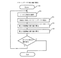
次に、本実施形態のCADデータの処理方法のフロー、及びCADデータが表示される表示画面について、図面を参照して説明する。図1及び図2は、本実施形態に係るCADデータの処理方法を示すフロー図である。図1はメインルーチンを示し、図2は図1のサブルーチンを示している。また、図3は、本実施形態に係るCADデータから抽出されたパターンデータを示す図である。また、図4は、本実施形態に係るCADデータの表示画面を示している。なお、図3及び図4では、図5に示したものと同様の構成要素については、同一の符号を付して説明を行うものとする。 Next, a flow of a CAD data processing method according to the present embodiment and a display screen on which CAD data is displayed will be described with reference to the drawings. 1 and 2 are flowcharts showing a CAD data processing method according to this embodiment. FIG. 1 shows the main routine, and FIG. 2 shows the subroutine of FIG. FIG. 3 is a diagram showing pattern data extracted from CAD data according to the present embodiment. FIG. 4 shows a display screen of CAD data according to the present embodiment. 3 and 4, the same components as those shown in FIG. 5 are described with the same reference numerals.
図1のメインルーチンに示すように、ステップA1では、CADシステムにCADデータが読み込まれる。また、CADシステムには、製造プロセスに必要な複数の工程の工程名が含まれた工程管理情報が読み込まれる。ここで、複数の工程名は、N個の工程名であるものとする。なお、これらのCADデータの読み込み、もしくは工程管理情報の読み込みは、いわゆるリダイレクション機能(オペレーティングシステムによるデータファイルの入出力機能)等を用いてユーザの操作により行われるが、プログラムにより自動的に行われてもよい。 As shown in the main routine of FIG. 1, in step A1, CAD data is read into the CAD system. In addition, process management information including process names of a plurality of processes necessary for the manufacturing process is read into the CAD system. Here, the plurality of process names are assumed to be N process names. The reading of the CAD data or the process management information is performed by a user operation using a so-called redirection function (data file input / output function by the operating system) or the like, but is automatically performed by a program. May be.
次に、ステップA2では、工程管理情報に含まれるN個の工程名と、CADデータを構成する複数のパターンデータを参照して、各工程名に対応するパターンデータを検索する。そして、工程名と、それに対応するパターンデータの組は、第1の記憶領域に格納される。工程名に対応するパターンデータが存在しない場合には、工程名のみが第1の記憶領域に格納される。 Next, in step A2, the pattern data corresponding to each process name is searched with reference to N process names included in the process management information and a plurality of pattern data constituting CAD data. A set of process names and corresponding pattern data is stored in the first storage area. If there is no pattern data corresponding to the process name, only the process name is stored in the first storage area.
次に、ステップA3では、各パターンデータの第1の座標軸における各最大幅xi(i=1,2,・・・N)、及び第2の座標軸における各最大幅yi(i=1,2,・・・N)を算出する。ここで、パターンデータの各最大幅xi,yiとは、言い換えれば、そのパターンデータの全ての座標点を包含する最小の矩形(いわゆるバウンダリーボックス)の第1及び第2の座標軸に沿った各辺の長さである。 Next, in step A3, each maximum width xi (i = 1, 2,... N) of each pattern data on the first coordinate axis and each maximum width yi (i = 1, 2,... N) on the second coordinate axis. ... N) is calculated. Here, each maximum width xi, yi of the pattern data is, in other words, each of the minimum rectangles (so-called boundary boxes) including all coordinate points of the pattern data along the first and second coordinate axes. The length of the side.
上記第1及び第2の座標軸における各最大幅xi,yiの算出は、例えば図2のサブルーチンのように行われる。即ち、ステップB1ではN個の工程名の中から1つの工程名を選択し、それに対応するパターンデータを抽出する。そして、ステップB2では、そのパターンデータの第1の方向の最大幅xiを算出する。その算出は、例えば次のように行われる。 The calculation of the maximum widths xi and yi on the first and second coordinate axes is performed, for example, in a subroutine of FIG. That is, in step B1, one process name is selected from N process names, and pattern data corresponding to it is extracted. In step B2, the maximum width xi in the first direction of the pattern data is calculated. The calculation is performed as follows, for example.
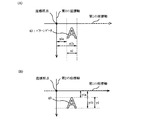
まず、そのパターンデータに含まれる各座標点について、第1の座標軸における座標原点からの距離を算出する。次に、図3(A)に示すように、それらの距離の中から、最小値xia及び最大値xibを検索し、それらの差の絶対値を算出する。この絶対値を第1の座標軸における最大幅xiとする。 First, for each coordinate point included in the pattern data, the distance from the coordinate origin on the first coordinate axis is calculated. Next, as shown in FIG. 3A, the minimum value xia and the maximum value xib are searched from these distances, and the absolute value of the difference between them is calculated. This absolute value is taken as the maximum width xi on the first coordinate axis.
次に、ステップB3では、ステップB1で選択した工程名に対応するパターンデータの第2の方向の最大幅yiを算出する。その算出は、例えば第1の方向の最大幅xiと同様に次のように行われる。 Next, in step B3, the maximum width yi in the second direction of the pattern data corresponding to the process name selected in step B1 is calculated. The calculation is performed as follows, for example, similarly to the maximum width xi in the first direction.
まず、そのパターンデータに含まれる各座標点について、第2の座標軸における座標原点からの距離を算出する。次に、図3(B)に示すように、それらの距離の中から、最小値yia及び最大値yibを検索し、それらの差の絶対値を算出する。この絶対値を第2の座標軸における最大幅yiとする。 First, for each coordinate point included in the pattern data, the distance from the coordinate origin on the second coordinate axis is calculated. Next, as shown in FIG. 3B, the minimum value yia and the maximum value yib are searched from these distances, and the absolute value of the difference between them is calculated. This absolute value is taken as the maximum width yi on the second coordinate axis.
以上に示したパターンデータの最大幅xi,yiの算出を、全ての工程名が選択されるまで繰り返し、全てのパターンデータの最大幅xi,yiの算出を行う。なお、選択された工程名に対応するパターンデータが存在しない場合、いわゆるNULLデータとして、例えば、最大幅xi,yiは零とする。こうして算出された各パターンデータの第1及び第2の座標軸における最大幅xi,yiは、例えばバッファ等の第2の記憶領域に格納される。 The calculation of the maximum widths xi, yi of the pattern data described above is repeated until all process names are selected, and the maximum widths xi, yi of all the pattern data are calculated. When there is no pattern data corresponding to the selected process name, for example, the maximum widths xi and yi are set to zero as so-called NULL data. The maximum widths xi and yi on the first and second coordinate axes of each pattern data calculated in this way are stored in a second storage area such as a buffer.
次に、図1のメインルーチンのステップA4では、工程管理情報に含まれる複数の工程名の中から1つの工程名が選択される。この工程名の選択は、好ましくは製造プロセスの工程順に従って行われる。そして、第1の記憶領域を参照して、選択した工程名に対応するパターンデータを選択し、そのパターンデータのみをCADデータから抽出する。 Next, in step A4 of the main routine of FIG. 1, one process name is selected from a plurality of process names included in the process management information. The selection of the process name is preferably performed according to the process sequence of the manufacturing process. Then, with reference to the first storage area, pattern data corresponding to the selected process name is selected, and only the pattern data is extracted from the CAD data.
そして、図4に示すように、選択した工程名に対応するパターンデータが存在する場合(即ち、最大幅xi,yiが零でない場合)、その工程名と共に、それに対応するパターンデータ40を表示画面10のパターンデータ表示領域11に表示する。この工程名及びパターンデータ40の表示の際には、ステップA5及びステップA6において、第2の記憶領域を参照して、パターンデータ40の第2の座標軸における最大幅yiに所定の距離αを加えたシフト幅Lsの分だけ、パターンデータ40を第2の座標軸に沿ってシフトさせて表示する。ここで、所定の距離αは、複数の工程名及びパターンデータ40が第2の座標軸に沿って繰り返し表示されても、それらが互いに重畳しないようなシフト幅Lsが得られるように、任意の距離で設定される。また、パターンデータ40は、第1の座標軸においてはシフトされずに、本来の座標を保ったまま表示されている。
Then, as shown in FIG. 4, when there is pattern data corresponding to the selected process name (that is, when the maximum widths xi and yi are not zero), the
なお、図示しないが、必要に応じて、上記パターンデータ40の表示の際、パターンデータ40を、その第1の座標軸における最大幅xiを基準として、第1の座標軸に沿ってシフトさせて表示してもよい。
Although not shown, when the
一方、選択された工程名に対応するパターンデータが存在しない場合、ステップA7では、第2の記憶領域を参照して、第2の座標軸における各最大幅yiの中から最大値ymaxを検索し、その最大値ymaxをシフト幅Lsとする。もしくは、その最大値ymaxに上記所定の距離αを加えて、これをシフト幅Lsとする。そして、そのシフト幅Lsを以って、その工程名を第2の座標軸に沿ってシフトさせて表示させる。このとき、その工程名は、対応するパターンデータが存在しないことをユーザに対して明示するようにして、例えば点滅表示される。また、本来ならばパターンデータ40が表示される領域では、上記シフト幅Lsの範囲を、何も表示されない非表示領域とする。これにより、パターンデータが存在しない工程名の視認性を確実に高めることができる。
On the other hand, if there is no pattern data corresponding to the selected process name, in step A7, the maximum value ymax is searched from the maximum widths yi on the second coordinate axis with reference to the second storage area, The maximum value ymax is defined as a shift width Ls. Alternatively, the predetermined distance α is added to the maximum value ymax, and this is set as the shift width Ls. Then, the process name is shifted and displayed along the second coordinate axis with the shift width Ls. At this time, the process name is displayed in a blinking manner, for example, so as to clearly indicate to the user that the corresponding pattern data does not exist. Further, in the area where the
このステップA4乃至A7を、全ての工程名が選択されるまでN回繰り返す。こうして、図4に示すように、各工程及びそれに対応する各パターンデータ40を、互いに重畳させずに、同時に並列させて表示することができる。
Steps A4 to A7 are repeated N times until all process names are selected. In this way, as shown in FIG. 4, each process and each
なお、複数のパターンデータ40が重なり合ったCADデータは、表示画面10の所定の領域、例えばCADデータ表示領域12において表示されてもよい。もしくは、このCADデータ表示領域12では、読み込まれたCADデータが、読み込まれた工程管理情報のいずれの工程名にも対応しないパターンデータを含んでいた場合、そのパターンデータのみが表示されてもよい。その場合、ステップA4で選択された工程名に対応するパターンデータ40がCADデータから抽出される度に、そのパターンデータ40をCADデータから削除し、残ったパターンデータをCADデータ表示領域12に表示させればよい。
The CAD data in which the plurality of
こうして、本実施形態によれば、各工程名及びそれに対応する各パターンデータ40を第2の座標軸に沿って互いに重畳しないように並列して表示することが可能となる。そのため、CADシステムのユーザが、CADデータを構成する複数のパターンデータ40の正誤を確認する際に、従来例のように、1つの工程名に対応するパターンデータ40の抽出と表示を、複数の工程名に対して繰り返さなくともよい。即ち、CADシステムのユーザにとってCADデータの正誤の確認が容易となる。
Thus, according to the present embodiment, each process name and each
また、表示画面10に表示されたパターンデータ40の第1の座標軸が固定されている場合、第1の座標軸に関する各パターンデータ40間の配置関係を、ユーザが容易に確認することができる。結果として、半導体集積回路の自動設計において、CADシステムのユーザの負担を大幅に軽減することが可能となる。
Moreover, when the 1st coordinate axis of the
なお、上記実施形態では、パターンデータの第1及び第2の最大幅を算出するステップ(図2のステップB2及びB3)は、ステップA3として、図2のサブルーチン内で行われたが、本発明はこれに限定されない。即ち、パターンデータの第1及び第2の最大幅を算出するステップB2及びステップB3は、図1のメインルーチンのループ内において、ステップA4の後に行われてもよい。 In the above-described embodiment, the step of calculating the first and second maximum widths of the pattern data (steps B2 and B3 in FIG. 2) is performed in the subroutine of FIG. 2 as step A3. Is not limited to this. That is, step B2 and step B3 for calculating the first and second maximum widths of the pattern data may be performed after step A4 in the loop of the main routine of FIG.
また、上記実施形態では、第1及び第2の座標軸における各最大幅xi,yiを算出するものとしたが、本発明はこれに限定されない。即ち、パターンデータを第1の座標軸に沿ってシフトさせて表示する必要がなければ、第1の座標軸における最大幅xiを算出するステップB2は省略されてもよい。 In the above embodiment, the maximum widths xi and yi on the first and second coordinate axes are calculated. However, the present invention is not limited to this. That is, if it is not necessary to shift and display the pattern data along the first coordinate axis, the step B2 for calculating the maximum width xi on the first coordinate axis may be omitted.
10 表示画面
11 パターンデータ表示領域 12 CADデータ表示領域
30 CADデータ 40 パターンデータ
10 Display screen 11 Pattern data display area 12 CAD data display
Claims (5)
前記CADデータと、複数の工程名からなる工程管理情報を、前記CADシステムに読み込むステップと、
前記CADデータから各工程名に対応する前記パターンデータをそれぞれ抽出し、前記第2の座標軸における各パターンデータの各最大幅を算出するステップと、
各パターンデータを、各最大幅に基づく各シフト幅を以って、前記第2の座標軸に沿って互いに重ならないように順次シフトさせながら、各パターンデータに対応する各工程名と共に前記画面上に表示するステップと、を含むことを特徴とするCADデータの処理方法。 In a CAD system for automatically designing a semiconductor device, a CAD data processing method for displaying on a screen CAD data in which a plurality of pattern data corresponding to first and second coordinate axes are overlapped,
Reading the CAD data and process management information comprising a plurality of process names into the CAD system;
Extracting each pattern data corresponding to each process name from the CAD data, and calculating each maximum width of each pattern data in the second coordinate axis;
Each pattern data is shifted on the screen along with the process names corresponding to each pattern data while sequentially shifting the pattern data so as not to overlap each other with the respective shift widths based on the respective maximum widths. And a step of displaying the CAD data.
前記パターンデータに含まれる各座標点について、前記第2の座標軸における座標原点からの距離を算出するステップと、
前記距離の最小値と最大値の差を算出し、その差の絶対値を前記最大幅として決定するステップと、を含むことを特徴とする請求項1記載のCADデータの処理方法。 Calculating the maximum width of the pattern data on the second coordinate axis;
For each coordinate point included in the pattern data, calculating a distance from the coordinate origin in the second coordinate axis;
The CAD data processing method according to claim 1, further comprising: calculating a difference between the minimum value and the maximum value of the distance and determining an absolute value of the difference as the maximum width.
Priority Applications (1)
| Application Number | Priority Date | Filing Date | Title |
|---|---|---|---|
| JP2005199306A JP2007018281A (en) | 2005-07-07 | 2005-07-07 | Processing method of cad data |
Applications Claiming Priority (1)
| Application Number | Priority Date | Filing Date | Title |
|---|---|---|---|
| JP2005199306A JP2007018281A (en) | 2005-07-07 | 2005-07-07 | Processing method of cad data |
Publications (1)
| Publication Number | Publication Date |
|---|---|
| JP2007018281A true JP2007018281A (en) | 2007-01-25 |
Family
ID=37755402
Family Applications (1)
| Application Number | Title | Priority Date | Filing Date |
|---|---|---|---|
| JP2005199306A Pending JP2007018281A (en) | 2005-07-07 | 2005-07-07 | Processing method of cad data |
Country Status (1)
| Country | Link |
|---|---|
| JP (1) | JP2007018281A (en) |
Citations (4)
| Publication number | Priority date | Publication date | Assignee | Title |
|---|---|---|---|---|
| JPH05281903A (en) * | 1992-04-02 | 1993-10-29 | Nissan Motor Co Ltd | Navigation device for vehicle |
| JPH06143090A (en) * | 1992-11-10 | 1994-05-24 | Sekisui Chem Co Ltd | Nc data origination system |
| JPH07200691A (en) * | 1993-12-28 | 1995-08-04 | Kansai Electric Power Co Inc:The | Data management method |
| JP2005084725A (en) * | 2003-09-04 | 2005-03-31 | Canon Inc | Process flow generation device and process flow generation method |
-
2005
- 2005-07-07 JP JP2005199306A patent/JP2007018281A/en active Pending
Patent Citations (4)
| Publication number | Priority date | Publication date | Assignee | Title |
|---|---|---|---|---|
| JPH05281903A (en) * | 1992-04-02 | 1993-10-29 | Nissan Motor Co Ltd | Navigation device for vehicle |
| JPH06143090A (en) * | 1992-11-10 | 1994-05-24 | Sekisui Chem Co Ltd | Nc data origination system |
| JPH07200691A (en) * | 1993-12-28 | 1995-08-04 | Kansai Electric Power Co Inc:The | Data management method |
| JP2005084725A (en) * | 2003-09-04 | 2005-03-31 | Canon Inc | Process flow generation device and process flow generation method |
Similar Documents
| Publication | Publication Date | Title |
|---|---|---|
| US6829754B1 (en) | Method and system for checking for power errors in ASIC designs | |
| TWI423057B (en) | Layout versus schematic error system and method | |
| US9047437B2 (en) | Method, system and software for accessing design rules and library of design features while designing semiconductor device layout | |
| US6536023B1 (en) | Method and system for hierarchical metal-end, enclosure and exposure checking | |
| TWI476617B (en) | Method and system for automatic generation of solutions for circuit design rule violations | |
| US20120047479A1 (en) | Incremental Layout Analysis | |
| US7665050B2 (en) | Semiconductor device verification system and semiconductor device fabrication method | |
| US8984459B2 (en) | Methods and apparatus for layout verification | |
| CN106200273B (en) | Method for detecting photoetching hot spot | |
| JP2006259943A (en) | Integrated circuit layout design system, its method and program | |
| US10339246B2 (en) | Schematic overlay for design and verification | |
| US9304981B1 (en) | System and method for providing an inter-application overlay to communicate information between users and tools in the EDA design flow | |
| JP2006344176A (en) | Macro arrangement design device with consideration given to density, program, and design method | |
| JPH08212241A (en) | Design method for mask pattern for semiconductor integrated circuit or directly plotting pattern on wafer and their design rule confirming method | |
| US9697315B2 (en) | System and method for displaying a device using an automated tool | |
| JP2007018281A (en) | Processing method of cad data | |
| JP2008277497A (en) | Design system of semiconductor integrated circuit, design method of semiconductor integrated circuit, manufacturing method of semiconductor device and semiconductor device | |
| JP5020003B2 (en) | Reticle verification system and program | |
| JPH056412A (en) | Interactive wiring system | |
| JP2007086979A (en) | Test pattern editing device | |
| JP4140013B2 (en) | Semiconductor integrated circuit gate resizing apparatus and method and program thereof | |
| JP2009302179A (en) | Layout system and layout method for semiconductor integrated circuit | |
| JP5309728B2 (en) | Reticle data creation method and reticle data creation device | |
| JP4455148B2 (en) | Cell layout drawing creation apparatus and method, and program | |
| JP2008304716A (en) | System and program for designing reticle |
Legal Events
| Date | Code | Title | Description |
|---|---|---|---|
| A621 | Written request for application examination |
Free format text: JAPANESE INTERMEDIATE CODE: A621 Effective date: 20080701 |
|
| A131 | Notification of reasons for refusal |
Free format text: JAPANESE INTERMEDIATE CODE: A131 Effective date: 20101027 |
|
| A521 | Written amendment |
Free format text: JAPANESE INTERMEDIATE CODE: A523 Effective date: 20101215 |
|
| A02 | Decision of refusal |
Free format text: JAPANESE INTERMEDIATE CODE: A02 Effective date: 20110107 |