JP2007017198A - Overcurrent detection device - Google Patents
Overcurrent detection device Download PDFInfo
- Publication number
- JP2007017198A JP2007017198A JP2005196616A JP2005196616A JP2007017198A JP 2007017198 A JP2007017198 A JP 2007017198A JP 2005196616 A JP2005196616 A JP 2005196616A JP 2005196616 A JP2005196616 A JP 2005196616A JP 2007017198 A JP2007017198 A JP 2007017198A
- Authority
- JP
- Japan
- Prior art keywords
- voltage
- current
- circuit
- variation
- overcurrent
- Prior art date
- Legal status (The legal status is an assumption and is not a legal conclusion. Google has not performed a legal analysis and makes no representation as to the accuracy of the status listed.)
- Pending
Links
Images
Landscapes
- Measurement Of Current Or Voltage (AREA)
- Emergency Protection Circuit Devices (AREA)
- Protection Of Static Devices (AREA)
Abstract
Description
本発明は、例えば直流負荷回路をオン、オフ動作するための半導体スイッチの端子間電圧を増幅し、増幅後の電圧と基準となる過電流判定電圧とを比較して、過電流の発生を検出する過電流検出装置に関する。 The present invention, for example, amplifies a voltage between terminals of a semiconductor switch for turning on / off a DC load circuit, compares the amplified voltage with a reference overcurrent determination voltage, and detects the occurrence of an overcurrent. The present invention relates to an overcurrent detection device.
例えば、車両に搭載されるパワーウインド駆動用のモータを制御する負荷制御回路では、直流電源とモータとの間にFET等の半導体スイッチを設け、該半導体スイッチのオン、オフを切り替えることにより、モータの駆動、停止を制御する。また、このような負荷制御回路では、負荷、或いはハーネスに短絡電流等の過電流が流れた際に、これを検出する過電流検出回路が備えられており、過電流を検出した際には、即時に半導体スイッチを遮断して半導体スイッチを含む回路全体を保護する(例えば、特許文献1参照)。 For example, in a load control circuit for controlling a motor for driving a power window mounted on a vehicle, a semiconductor switch such as an FET is provided between a DC power supply and the motor, and the semiconductor switch is turned on and off to Controls driving and stopping of Further, in such a load control circuit, when an overcurrent such as a short circuit current flows in the load or the harness, an overcurrent detection circuit for detecting this is provided, and when an overcurrent is detected, The semiconductor switch is immediately shut off to protect the entire circuit including the semiconductor switch (see, for example, Patent Document 1).
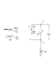
図2は、従来における負荷制御回路の構成を示す回路図である。同図に示すように、負荷制御回路はバッテリVBと、モータ等の負荷101と、スイッチング用のFET(T101)と、を備えており、バッテリVBのプラス端子とFET(T101)のドレインが接続され、該FET(T101)のソースと負荷101の一端が接続され、他端とバッテリVBのマイナス端子がグランドに接地されている。
FIG. 2 is a circuit diagram showing a configuration of a conventional load control circuit. As shown in the figure, the load control circuit includes a battery VB, a
また、FET(T101)のドレイン(電圧V1)は、抵抗R101,R102の直列接続回路を介してグランドに接地されている。そして、抵抗R101とR102の接続点(電圧V4)は比較器CMP101のマイナス側入力端子に接続されている。 The drain (voltage V1) of the FET (T101) is grounded through a series connection circuit of resistors R101 and R102. The connection point (voltage V4) between the resistors R101 and R102 is connected to the negative side input terminal of the comparator CMP101.
更に、FET(T101)のソース(電圧V2)は、比較器CMP101のプラス側入力端子に接続されている。また、FET(T101)のオン、オフを制御するためのドライバ102を備えており、該ドライバ102の出力端子は、抵抗R103を介してFET(T101)のゲートに接続されている。
Further, the source (voltage V2) of the FET (T101) is connected to the plus side input terminal of the comparator CMP101. Further, a
ここで、FET(T101)のドレイン、ソース間電圧VDSは、FET(T101)のオン抵抗をRon、ドレイン電流をIDとすると、次の(1)式にて示すことができる。 Here, the drain-source voltage VDS of the FET (T101) can be expressed by the following equation (1), where Ron is the on-resistance of the FET (T101) and ID is the drain current.
VDS=V1−V2=Ron*ID …(1)
そして、負荷101に過電流が流れ、IDが過電流状態となると、電圧VDSが増大し、(V1−V2)>(V1−V4)となり、比較器CMP101の出力信号が反転することにより、後段の回路(図示省略)にて過電流状態が検出され、ドライバ102へ駆動停止信号を出力する。その結果、FET(T101)がオフとされるので、回路を過電流から保護することができる。
VDS = V1-V2 = Ron * ID (1)
Then, when overcurrent flows through the
ここで、過電流として検出されるIDを過電流検出値Iovc、比較器CMP101のオフセット電圧をVoffとすると、次の(2)式が得られる。 Here, when the ID detected as an overcurrent is an overcurrent detection value Iovc and the offset voltage of the comparator CMP101 is Voff, the following equation (2) is obtained.
V4=Ron*Iovc±Voff …(2)
上記(2)式より次の(3)式が得られる。
V4 = Ron * Iovc ± Voff (2)
The following equation (3) is obtained from the above equation (2).
Iovc=(V4/Ron)±(Voff/Ron) …(3)
ここで、比較器CMP101にオフセット電圧Voffが存在しなければ、即ち、Voff=0であれば、過電流検出値Iovcは電圧V4及びFET(T101)のオン抵抗Ronで決まる一定値となる。しかし、比較器CMP101にオフセット電圧Voffが存在すると、過電流検出値Iovcがばらつき、そのばらつき量は、±Voff/Ronとなる。つまり、同一のオフセット電圧Voffに対しては、オン抵抗Ronが小さいほど、過電流検出値Iovcのばらつき幅が大きくなる。
Iovc = (V4 / Ron) ± (Voff / Ron) (3)
Here, if the offset voltage Voff does not exist in the comparator CMP101, that is, if Voff = 0, the overcurrent detection value Iovc is a constant value determined by the voltage V4 and the ON resistance Ron of the FET (T101). However, if the offset voltage Voff exists in the comparator CMP101, the overcurrent detection value Iovc varies, and the variation amount becomes ± Voff / Ron. That is, for the same offset voltage Voff, the variation width of the overcurrent detection value Iovc increases as the on-resistance Ron decreases.
比較器CMP101のオフセット電圧(±Voff)のばらつき幅は、IC化のプロセスに依存し、通常のICでは±10[mV]程度となる。
上記したように、比較器CMP101のオフセット電圧Voffは、過電流検出値のばらつきの要因となり、過電流検出値の精度を低下させてしまうという問題が発生する。更に、今後FETのオン抵抗Ronが小さくなる傾向が進むと、より一層ばらつき幅が増大し、精度低下は益々大きくなり、何とか比較器CMP101のオフセット電圧の影響を低減したいという要望が高まっていた。 As described above, the offset voltage Voff of the comparator CMP101 causes a variation in the overcurrent detection value, which causes a problem that the accuracy of the overcurrent detection value is reduced. Furthermore, if the on-resistance Ron of the FET tends to become smaller in the future, the variation width further increases and the accuracy decrease becomes more and more, and there is an increasing desire to somehow reduce the influence of the offset voltage of the comparator CMP101.
本発明は、このような従来の課題を解決するためになされたものであり、その目的とするところは、オン抵抗Ronが小さい場合でも、比較器CMP101のオフセット電圧Voffの影響を低減して高精度な過電流検出が可能な過電流検出装置を提供することにある。 The present invention has been made to solve such a conventional problem. The object of the present invention is to reduce the influence of the offset voltage Voff of the comparator CMP101 even when the on-resistance Ron is small. An object of the present invention is to provide an overcurrent detection device capable of accurate overcurrent detection.
上記目的を達成するため、本願請求項1に記載の発明は、直流電源と負荷の間に半導体スイッチを備え、半導体スイッチのプラス側端子電圧(V1)とマイナス側端子電圧(V2)の電圧差(VDS)を用いて、半導体スイッチがオン、オフを制御する負荷回路の、過電流を検出する過電流検出装置において、前記半導体スイッチがオンしているとき、該半導体スイッチのプラス側端子電圧(V1)とマイナス側端子電圧(V2)のいずれよりも低い電圧となるように基準電圧(V3)を設け、前記半導体スイッチのプラス側端子電圧(V1)と基準電圧(V3)の差(V1−V3)に比例する電流(I1)を生成する第1の電流発生回路と、前記半導体スイッチのマイナス側端子電圧(V2)と基準電圧(V3)の差(V2−V3)に比例する電流(I3)を生成する第2の電流発生回路と、前記第1の電流発生回路で生成された電流(I1)と前記第2の電流発生回路で生成された電流(I3)との差分電流(I1−I3)を流すことにより、前記半導体スイッチの端子間電圧(V1−V2=VDS)に比例した大きさの電圧を生成する基準抵抗(R16)と、を備え、前記基準抵抗により生成された電圧を、前記端子間電圧(VDS)に加算して得られる加算電圧と、予め設定した過電流判定電圧とを比較し、前記加算電圧が前記過電流判定電圧を上回った際に過電流の発生を検出することを特徴とする。 In order to achieve the above object, the invention described in claim 1 of the present application includes a semiconductor switch between a DC power source and a load, and a voltage difference between a positive terminal voltage (V1) and a negative terminal voltage (V2) of the semiconductor switch. (VDS), an overcurrent detection device for detecting an overcurrent of a load circuit that controls on / off of the semiconductor switch, when the semiconductor switch is on, the positive terminal voltage ( V1) and a negative terminal voltage (V2) are provided with a reference voltage (V3) so as to be a lower voltage, and the difference (V1−) between the positive terminal voltage (V1) and the reference voltage (V3) of the semiconductor switch. A first current generation circuit that generates a current (I1) proportional to V3) and a difference (V2−V3) between the negative terminal voltage (V2) of the semiconductor switch and the reference voltage (V3). A second current generation circuit for generating a current (I3), and a difference current between the current (I1) generated by the first current generation circuit and the current (I3) generated by the second current generation circuit A reference resistor (R16) that generates a voltage proportional to the voltage (V1-V2 = VDS) between the terminals of the semiconductor switch by flowing (I1-I3), and is generated by the reference resistor The added voltage obtained by adding the obtained voltage to the terminal voltage (VDS) is compared with a preset overcurrent determination voltage, and when the added voltage exceeds the overcurrent determination voltage, the overcurrent It is characterized by detecting occurrence.
請求項2に記載の発明は、前記第1の電流と同一となる電流(I2=I1)を生成して、前記基準抵抗の一端側より流出させる第1のカレントミラー回路と、前記第2の電流と同一となる電流(I4=I3)を生成して、前記基準抵抗の一端側に流入させる第2のカレントミラー回路と、を備えることにより、前記基準抵抗に差分電流(I2−I4=I1−I3)を流すことを特徴とする。 According to a second aspect of the present invention, there is provided a first current mirror circuit that generates a current (I2 = I1) that is the same as the first current and causes the current to flow out from one end side of the reference resistor; A second current mirror circuit that generates a current (I4 = I3) that is the same as the current and flows it into one end of the reference resistor, thereby providing a differential current (I2−I4 = I1) in the reference resistor. -I3) is flowed.
請求項3に記載の発明は、前記第1のカレントミラー回路、及び第2のカレントミラー回路は、トランジスタ及び縮退抵抗を含むIC回路で構成され、前記トランジスタ特性のばらつきを前記縮退抵抗のばらつきに置き換えて、前記第1,第2のカレントミラー回路のばらつきが前記IC回路内部の縮退抵抗の抵抗値の相対ばらつきにのみ依存するようにしたことを特徴とする。 According to a third aspect of the present invention, the first current mirror circuit and the second current mirror circuit are configured by an IC circuit including a transistor and a degeneration resistor, and the variation in the transistor characteristics is changed to the variation in the degeneration resistance. In other words, the variation of the first and second current mirror circuits is dependent only on the relative variation of the resistance value of the degeneration resistor in the IC circuit.
請求項1の発明では、基準抵抗により生成された電圧を、端子間電圧(VDS)に加算して得られる加算電圧(V5)と、予め設定した過電流判定電圧(V4)とを比較器にて比較し、加算電圧が前記過電流判定電圧を上回った際に過電流の発生を検出するので、比較器に入力される電圧が増幅され、比較器のオフセット電圧Voffによる影響を低減することができる。その結果、高精度な過電流検出が可能となり、半導体スイッチ及び負荷回路を過電流から確実に保護することができる。 According to the first aspect of the present invention, an added voltage (V5) obtained by adding the voltage generated by the reference resistor to the inter-terminal voltage (VDS) and a preset overcurrent determination voltage (V4) are used as a comparator. And the occurrence of an overcurrent is detected when the added voltage exceeds the overcurrent determination voltage, so that the voltage input to the comparator is amplified and the influence of the offset voltage Voff of the comparator can be reduced. it can. As a result, it is possible to detect the overcurrent with high accuracy, and to reliably protect the semiconductor switch and the load circuit from the overcurrent.
請求項2の発明では、第1のカレントミラー回路を用いて電流I1と同一となる電流I2を生成し、第2のカレントミラー回路を用いて電流I3と同一となる電流I4を生成し、これらの差分電流を基準抵抗に流すことにより、端子間電圧VDSに比例した大きさの電圧を生成するので、簡単な構成で端子間電圧VDSに比例した電圧を生成することができる。 In the second aspect of the invention, the first current mirror circuit is used to generate the current I2 that is the same as the current I1, and the second current mirror circuit is used to generate the current I4 that is the same as the current I3. Since a voltage having a magnitude proportional to the inter-terminal voltage VDS is generated by flowing the difference current of 1 through the reference resistor, a voltage proportional to the inter-terminal voltage VDS can be generated with a simple configuration.
請求項3の発明では、各カレントミラー回路を構成するトランジスタの特性のばらつきを、縮退抵抗の抵抗値の相対ばらつきのみに依存するようにしているので、カレントミラー回路全体のばらつきを低減することができる。即ち、IC回路の内部に設けられる抵抗は、湿度、温度などに起因してばらつきが発生しても、全体が同一にばらつくので、相対的なばらつきを抑制することができる。これに対してトランジスタは、ばらつきを抑えることができない。そこで、ばらつきを抵抗のみに依存させることにより、全体ばらつきを低減させることができる。 According to the third aspect of the present invention, the variation in the characteristics of the transistors constituting each current mirror circuit is dependent only on the relative variation in the resistance value of the degeneration resistor, so that the variation in the entire current mirror circuit can be reduced. it can. That is, even if the resistance provided in the IC circuit varies due to humidity, temperature, and the like, the whole varies in the same manner, so that relative variation can be suppressed. In contrast, the transistor cannot suppress variations. Thus, the overall variation can be reduced by making the variation depend only on the resistance.
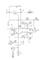
以下、本発明の実施形態を図面に基づいて説明する。図1は、本発明の一実施形態に係る過電流検出装置を含む直流負荷回路の構成を示す回路図である。同図に示すように、この直流負荷回路は、バッテリVBと、該バッテリVBより電力が供給されて駆動するモータ、ランプ等の負荷1と、ドレインがバッテリVBのプラス端子と接続されソースが負荷1の一端と接続されるFET(T1)と、抵抗R3を介してFET(T1)のゲートと接続され、該ゲートに駆動信号を出力するドライバ2とを備えている。 Hereinafter, embodiments of the present invention will be described with reference to the drawings. FIG. 1 is a circuit diagram showing a configuration of a DC load circuit including an overcurrent detection device according to an embodiment of the present invention. As shown in the figure, this DC load circuit includes a battery VB, a load 1 such as a motor and a lamp driven by power supplied from the battery VB, a drain connected to the positive terminal of the battery VB, and a source loaded. 1 includes a FET (T1) connected to one end of the terminal 1 and a driver 2 connected to the gate of the FET (T1) via a resistor R3 and outputting a drive signal to the gate.
そして、ドライバ2より出力される駆動信号によりFET(T1)のオン、オフが制御され、負荷1の駆動、停止を切り替えることができる。 Then, on / off of the FET (T1) is controlled by the drive signal output from the driver 2, and the driving and stopping of the load 1 can be switched.
また、FET(T1)のドレインとなる点P1は、抵抗R1とR2との直列接続回路を介してグランドに接地されており、抵抗R1とR2の接続点P4は、比較器CMP1のマイナス側入力端子に接続されている。なお、図1において抵抗R1,R2等の下に記載している数値、例えば抵抗R1の下に記載している「2K」は、この抵抗R1の抵抗値が一例として「2KΩ」であることを示している。 The point P1 serving as the drain of the FET (T1) is grounded via a series connection circuit of resistors R1 and R2, and the connection point P4 of the resistors R1 and R2 is a negative input of the comparator CMP1. Connected to the terminal. In FIG. 1, the numerical values described below the resistors R1, R2, etc., for example, “2K” described below the resistor R1, indicate that the resistance value of the resistor R1 is “2KΩ” as an example. Show.
他方、FET(T1)のソースとなる点P2(電圧V2)は、抵抗R16(基準抵抗)を介して比較器CMP1のプラス側入力端子となる点P5(電圧V5)に接続されている。 On the other hand, the point P2 (voltage V2) serving as the source of the FET (T1) is connected to the point P5 (voltage V5) serving as the plus side input terminal of the comparator CMP1 via the resistor R16 (reference resistor).
点P1は、抵抗R20,R21の直列接続回路を介してグランドに接地されており、2つの抵抗の接続点はFET(T9;PMOS)のゲートに接続され、該FET(T9)のドレインは接地され、ソース(点P3、電圧V3)は増幅回路の基準電圧になっている。 The point P1 is grounded through a series connection circuit of resistors R20 and R21, the connection point of the two resistors is connected to the gate of the FET (T9; PMOS), and the drain of the FET (T9) is grounded The source (point P3, voltage V3) is the reference voltage of the amplifier circuit.
カレントミラー回路(第1のカレントミラー回路)3は、ベース同士が互いに接続された2つのトランジスタT2,T3(NPN型)と、トランジスタT2のコレクタと点P1との間に配置された抵抗R10と、トランジスタT2のエミッタと点P3との間に配置された抵抗R11と、トランジスタT3のエミッタと点P3との間に配置された抵抗R12とを備えている。また、トランジスタT3のコレクタとなる点P5(電圧V5)は、比較器CMP1のプラス側入力端子に接続されている。 The current mirror circuit (first current mirror circuit) 3 includes two transistors T2 and T3 (NPN type) whose bases are connected to each other, a resistor R10 disposed between the collector of the transistor T2 and the point P1. A resistor R11 disposed between the emitter of the transistor T2 and the point P3, and a resistor R12 disposed between the emitter of the transistor T3 and the point P3. The point P5 (voltage V5) serving as the collector of the transistor T3 is connected to the plus side input terminal of the comparator CMP1.
第2のカレントミラー回路は、カレントミラー回路4及び5により構成され、カレントミラー回路4は、ベース同士が互いに接続された2つのトランジスタT4,T5(NPN型)と、トランジスタT5のコレクタと点P2との間に配置された抵抗R15と、トランジスタT5のエミッタと点P3との間に配置された抵抗R14と、トランジスタT4のエミッタと点P3との間に配置された抵抗R13とを備えている。また、トランジスタT4のコレクタは、カレントミラー回路5に接続されている。
The second current mirror circuit is composed of
カレントミラー回路5は、ヘッドルームとなる電源Vaddと、ゲート同士が互いに接続された2つのFET(T6,T7;PMOS)と、FET(T6)のソースと電源Vaddのプラス側出力端子との間に接続された抵抗R17と、FET(T7)のソースと電源Vaddのプラス側出力端子との間に接続された抵抗R18とを備えている。そして、FET(T6)のドレインは、点P5に接続され、FET(T7)のドレインは、トランジスタT4のコレクタに接続されている。 The current mirror circuit 5 includes a power supply Vadd serving as a headroom, two FETs (T6 and T7; PMOS) whose gates are connected to each other, a source of the FET (T6), and a positive output terminal of the power supply Vadd. And a resistor R18 connected between the source of the FET (T7) and the positive output terminal of the power supply Vadd. The drain of the FET (T6) is connected to the point P5, and the drain of the FET (T7) is connected to the collector of the transistor T4.
ここで、トランジスタT2に流れる電流をI1、トランジスタT3に流れる電流をI2、トランジスタT4に流れる電流、即ちFET(T7)に流れる電流をI5、トランジスタT5に流れる電流をI3、FET(T6)に流れる電流をI4とする。 Here, the current flowing through the transistor T2 is I1, the current flowing through the transistor T3 is I2, the current flowing through the transistor T4, that is, the current flowing through the FET (T7) is I5, the current flowing through the transistor T5 is flowing through I3, and the FET (T6). The current is I4.
次に、上記の如く構成された本実施形態に係る過電流検出装置の動作について説明する。 Next, the operation of the overcurrent detection device according to this embodiment configured as described above will be described.
ドライバ2より、FET(T1)のゲートに駆動信号が出力されと、該FET(T1)がオンとなり、バッテリVBより負荷1へ駆動用の電源電圧が印加され、電流IDが流れて負荷1を駆動させることができる。この際、FET(T1)のソース、ドレイン間には、電圧VDSが発生する。従って、点P1の電圧V1と点P2の電圧V2の差分(V1−V2)は、電圧VDSとなる。 When a drive signal is output from the driver 2 to the gate of the FET (T1), the FET (T1) is turned on, a power supply voltage for driving is applied from the battery VB to the load 1, and the current ID flows to cause the load 1 to flow. It can be driven. At this time, a voltage VDS is generated between the source and drain of the FET (T1). Therefore, the difference (V1−V2) between the voltage V1 at the point P1 and the voltage V2 at the point P2 becomes the voltage VDS.
また、電圧V1は、抵抗R1とR2で分圧され、接続点P4に発生する電圧V4が、過電流判定電圧として比較器CMP1のマイナス側入力端子に供給される。 The voltage V1 is divided by the resistors R1 and R2, and the voltage V4 generated at the connection point P4 is supplied to the negative input terminal of the comparator CMP1 as an overcurrent determination voltage.
更に、抵抗R20,R21の直列接続回路の両端には電圧V1が印加されるので、電圧V1を抵抗R20,R21で分圧した電圧がFET(T9)のゲートに加えられ、分圧された電圧に応じた大きさとなる電圧がFET(T9)のソースとなる点P3の電圧V3(以下、基準電圧V3という)となる。 Further, since the voltage V1 is applied to both ends of the series connection circuit of the resistors R20 and R21, a voltage obtained by dividing the voltage V1 by the resistors R20 and R21 is applied to the gate of the FET (T9), and the divided voltage is applied. The voltage corresponding to the voltage V3 at the point P3 that becomes the source of the FET (T9) (hereinafter referred to as the reference voltage V3).
基準電圧V3は、バッテリVBの電源電圧V1の大きさに連動して変化し、(V1−V3)がV1=12[V]で約0.9Vとなるように抵抗R20,R21の抵抗値を設定する。図1に示す例では、抵抗R20を100[KΩ]、抵抗R21を500[KΩ]としている。 The reference voltage V3 changes in conjunction with the power supply voltage V1 of the battery VB, and the resistance values of the resistors R20 and R21 are set so that (V1−V3) is about 0.9V when V1 = 12 [V]. Set. In the example shown in FIG. 1, the resistor R20 is 100 [KΩ] and the resistor R21 is 500 [KΩ].
カレントミラー回路3に設けられる抵抗R10、トランジスタT2、抵抗R11の直列接続回路には、電圧(V1−V3)が印加され、電流I1が流れる。また、トランジスタT3及び抵抗R12に流れる電流I2はI1と等しくなる。即ち、I1=I2である。 A voltage (V1-V3) is applied to the series connection circuit of the resistor R10, the transistor T2, and the resistor R11 provided in the current mirror circuit 3, and the current I1 flows. The current I2 flowing through the transistor T3 and the resistor R12 is equal to I1. That is, I1 = I2.
また、カレントミラー回路4に設けられる抵抗R15、トランジスタT5、抵抗R14の直列接続回路には、電圧(V2−V3)が印加され、電流I3が流れる。また、トランジスタT4及び抵抗R13に流れる電流I5は、I3と等しくなる。即ち、I3=I5である。ここで、抵抗R15=R10、抵抗R14=R11となるように抵抗値を設定する。
A voltage (V2-V3) is applied to the series connection circuit of the resistor R15, the transistor T5, and the resistor R14 provided in the
更に、上記の電流I5は、カレントミラー回路5に設けられる抵抗R18及びFET(T7)に流れる電流と等しくなっている。従って、抵抗R17及びFET(T6)に流れる電流I4はI5と等しいので、結果として電流I4は電流I3と等しくなる。 Further, the current I5 is equal to the current flowing through the resistor R18 and the FET (T7) provided in the current mirror circuit 5. Therefore, the current I4 flowing through the resistor R17 and the FET (T6) is equal to I5, and as a result, the current I4 is equal to the current I3.
ここで、比較器CMP1のプラス側入力端子となる点P5には、電流I4が流入し、電流I2が流出している。また、点P5から比較器CMP1を見たときのインピーダンスは無限大であるから、電流I2とI4の差分は、抵抗R16を介して図中の右側から左側に向けて流れる。換言すれば、電流(I2−I4)=(I1−I3)が抵抗R16の右側から左側に向けて流れることになる。 Here, the current I4 flows in and the current I2 flows out to the point P5 serving as the plus side input terminal of the comparator CMP1. Since the impedance when the comparator CMP1 is viewed from the point P5 is infinite, the difference between the currents I2 and I4 flows from the right side to the left side in the figure via the resistor R16. In other words, the current (I2-I4) = (I1-I3) flows from the right side to the left side of the resistor R16.
ここで、トランジスタT2及びT5のベース、エミッタ間電圧をそれぞれVbe2、Vbe5とすると、(I1−I3)は、以下の(4)式で示すことができる。 Here, assuming that the base-emitter voltages of the transistors T2 and T5 are Vbe2 and Vbe5, respectively, (I1-I3) can be expressed by the following equation (4).
I1−I3=(V1−Vbe2−V3)/(R10+R11)
−(V2−Vbe5−V3)/(R15+R14) …(4)
ここで、R10=R15、R11=R14であり、Vbe2=Vbe5であるから、上記(4)式は、次の(5)式となる。
I1-I3 = (V1-Vbe2-V3) / (R10 + R11)
-(V2-Vbe5-V3) / (R15 + R14) (4)
Here, since R10 = R15, R11 = R14, and Vbe2 = Vbe5, the above equation (4) becomes the following equation (5).
I1−I3=(V1−V2)/(R10+R11) …(5)
ここで、抵抗R16の抵抗値が、R10+R11に等しくなるように設定すると、抵抗R16における電圧降下V16は、次の(6)式で示すことができる。
I1-I3 = (V1-V2) / (R10 + R11) (5)
Here, when the resistance value of the resistor R16 is set to be equal to R10 + R11, the voltage drop V16 in the resistor R16 can be expressed by the following equation (6).
V16=R16*(I1−I3)
=R16*(V1−V2)/(R10+R11)
=V1−V2 …(6)
従って、比較器CMP1により過電流判定電圧(V1−V4)と比較される電圧(V1−V5)は、次の(7)式で示すことができる。
V16 = R16 * (I1-I3)
= R16 * (V1-V2) / (R10 + R11)
= V1-V2 (6)
Therefore, the voltage (V1-V5) compared with the overcurrent determination voltage (V1-V4) by the comparator CMP1 can be expressed by the following equation (7).
V1−V5=(V1−V2)+V16=2*(V1−V2) …(7)
即ち、FET(T1)のドレイン、ソース間電圧VDSとなる電圧(V1−V2)は、2倍に増幅されて、比較器CMP1のプラス側入力端子に供給されることになる。従って、FET(T1)のオン抵抗Ronが小さく、ドレイン、ソース間電圧VDSが小さい場合でも、これを増倍させて過電流判定電圧との比較が可能となるので、比較器CMP1のオフセット電圧Voffの影響を受けにくくすることができる。換言すれば、上述した(3)式の、(Voff/Ron)の項で、等価的にRonを大きくすることができるので、Voffの影響を軽減することができ、過電流判定の精度を向上させることができる。
V1-V5 = (V1-V2) + V16 = 2 * (V1-V2) (7)
That is, the voltage (V1-V2) that becomes the drain-source voltage VDS of the FET (T1) is amplified by a factor of 2 and supplied to the plus side input terminal of the comparator CMP1. Therefore, even when the on-resistance Ron of the FET (T1) is small and the drain-source voltage VDS is small, it can be multiplied and compared with the overcurrent determination voltage, so the offset voltage Voff of the comparator CMP1. Can be less affected by In other words, since Ron can be increased equivalently in the term (Voff / Ron) of the above-described equation (3), the influence of Voff can be reduced and the accuracy of overcurrent determination is improved. Can be made.
なお、上記の説明では、各トランジスタT2,T5のVbe2,Vbe5の動作抵抗を無視したが、実際には1.3[KΩ]程度の動作抵抗が存在するので、この動作抵抗分を加味して抵抗R16の抵抗値を設定している。即ち、図1に示す抵抗R10の抵抗値を5[KΩ]、抵抗R11の抵抗値を10[KΩ]とし、抵抗R16の抵抗値は、5+10+1.3=16.3[KΩ]としている。 In the above description, the operating resistances of Vbe2 and Vbe5 of the transistors T2 and T5 are ignored. However, since there is actually an operating resistance of about 1.3 [KΩ], this operating resistance is taken into account. The resistance value of the resistor R16 is set. That is, the resistance value of the resistor R10 shown in FIG. 1 is 5 [KΩ], the resistance value of the resistor R11 is 10 [KΩ], and the resistance value of the resistor R16 is 5 + 10 + 1.3 = 16.3 [KΩ].
次に、抵抗R16の両端に生じる電圧V16のばらつきについて説明する。本実施形態では、比較器CMP1のオフセット電圧Voffの影響を低減するために、抵抗R16を用いて電圧V16を発生させ、これをVDSに加算する方法を採用しているので、電圧V16及び各カレントミラー回路3,4,5に生じるばらつきが、上記のオフセット電圧Voffのばらつきよりも小さいことが条件となる。以下、詳述する。
Next, the variation in the voltage V16 generated across the resistor R16 will be described. In this embodiment, in order to reduce the influence of the offset voltage Voff of the comparator CMP1, a method of generating the voltage V16 using the resistor R16 and adding it to VDS is adopted. The condition is that the variation occurring in the
[V16のばらつきについて]
いま、下記のようにα、β、γ、δ1、δ2を決める。
[V16 variation]
Now, α, β, γ, δ1, and δ2 are determined as follows.
α:I1とI2の相対ばらつき
β:I3とI5の相対ばらつき
γ:I5とI4の相対ばらつき
δ1:R16と他の抵抗値の相対ばらつき
δ2:(R10+R11)と(R15+R14)の相対ばらつき
とすると、次の(8)式が得られる。
α: Relative variation between I1 and I2 β: Relative variation between I3 and I5 γ: Relative variation between I5 and I4 δ1: Relative variation between R16 and other resistance values δ2: Relative variation between (R10 + R11) and (R15 + R14) The following equation (8) is obtained.
V16=R16(1±δ1)(I2−I4)
=R16(1±δ1){I1(1±α)−I3(1±β)(1±γ)}
=R16(1±δ1)[{(V1−V2)+(V2−V3)−Vbe2}
/(R10+R11)*(1±α)−{(V2−V3)−Vbe5}
/(R15+R14)*(1±β)(1±γ)]
=R16(1±δ1)(V1−V2)
/(R10+R11)*(1±α)[1+{(V2−V3)−Vbe2}
/(V1−V2)−{(V2−V3)−Vbe5}
/(V1−V2)*(R10+R11)
/(R15+R14)*(1±β)*(1±γ)/(1±α)]
=R16(1±δ1)(V1−V2)
/(R10+R11)*(1±α)[1+{(V2−V3)−Vbe2}
/(V1−V2)−{(V2−V3)−Vbe5}
/(V1−V2)*(1±δ2)(1±β)(1±γ)/(1±α)]
…(8)
ここで、Vbe2=Vbe5とすると、次の(9)式が得られる。
V16 = R16 (1 ± δ1) (I2-I4)
= R16 (1 ± δ1) {I1 (1 ± α) −I3 (1 ± β) (1 ± γ)}
= R16 (1 ± δ1) [{(V1-V2) + (V2-V3) -Vbe2}
/ (R10 + R11) * (1 ± α) − {(V2−V3) −Vbe5}
/ (R15 + R14) * (1 ± β) (1 ± γ)]
= R16 (1 ± δ1) (V1-V2)
/ (R10 + R11) * (1 ± α) [1 + {(V2−V3) −Vbe2}
/ (V1-V2)-{(V2-V3) -Vbe5}
/ (V1-V2) * (R10 + R11)
/ (R15 + R14) * (1 ± β) * (1 ± γ) / (1 ± α)]
= R16 (1 ± δ1) (V1-V2)
/ (R10 + R11) * (1 ± α) [1 + {(V2−V3) −Vbe2}
/ (V1-V2)-{(V2-V3) -Vbe5}
/ (V1-V2) * (1 ± δ2) (1 ± β) (1 ± γ) / (1 ± α)]
(8)
Here, when Vbe2 = Vbe5, the following equation (9) is obtained.
V16=R16(1±δ1)(V1−V2)
/(R10+R11)*(1±α)[1+{(V2−V3)−Vbe2}
/(V1−V2){1−(1±δ2)(1±β)(1±γ)/(1±α)}
≒R16(1±δ1)(V1−V2)
/(R10+R11)*(1±α)[1+{(V2−V3)−Vbe2}
/(V1−V2){1−(1±δ2±β±γ±α)}]
=R16(1±δ1)(V1−V2)
/(R10+R11)*(1±α)[1+{(V2−V3)−Vbe2}
/(V1−V2)*(±δ2±β±γ±α)] …(9)
ここで、R16=R10+R11であるから、(10)が得られる。
V16 = R16 (1 ± δ1) (V1-V2)
/ (R10 + R11) * (1 ± α) [1 + {(V2−V3) −Vbe2}
/ (V1-V2) {1- (1 ± δ2) (1 ± β) (1 ± γ) / (1 ± α)}
≒ R16 (1 ± δ1) (V1-V2)
/ (R10 + R11) * (1 ± α) [1 + {(V2−V3) −Vbe2}
/ (V1-V2) {1- (1 ± δ2 ± β ± γ ± α)}]
= R16 (1 ± δ1) (V1-V2)
/ (R10 + R11) * (1 ± α) [1 + {(V2−V3) −Vbe2}
/ (V1-V2) * (± δ2 ± β ± γ ± α)] (9)
Here, since R16 = R10 + R11, (10) is obtained.
V16=(V1−V2)(1±δ1)(1±α)[1+{(V2−V3)−Vbe2}
/(V1−V2)*(±δ2±β±γ±α)] …(10)
VB=14.5Vのとき、CMP1が反転する(V1−V4)電圧は、190.8mVであるから、そのときのV1−V2は190.8/2=95.4mVとなる。シミュレーション結果から{(V2−V3)−Vbe2}=198.1mVとなるから、次の(11)式が得られる。
V16 = (V1-V2) (1 ± δ1) (1 ± α) [1 + {(V2-V3) -Vbe2}
/ (V1-V2) * (± δ2 ± β ± γ ± α)] (10)
When VB = 14.5V, the voltage at which CMP1 is inverted (V1-V4) is 190.8 mV, so V1-V2 at that time is 190.8 / 2 = 95.4 mV. From the simulation result, {(V2−V3) −Vbe2} = 198.1 mV, so the following equation (11) is obtained.
{(V2−V3)−Vbe2}/(V1−V2)=198.1mV/95.4mV
=2.08 …(11)
従って、(10)式は以下の(12)式となる。
{(V2-V3) -Vbe2} / (V1-V2) = 198.1 mV / 95.4 mV
= 2.08 (11)
Therefore, equation (10) becomes the following equation (12).
V16=(V1−V2)(1±δ1)(1±α)
*[1+2.08(±δ2±β±γ±α)] …(12)
ここで、V1−V3を小さく設定すれば係数は2.08よりは小さくなって行く。
V16 = (V1-V2) (1 ± δ1) (1 ± α)
* [1 + 2.08 (± δ2 ± β ± γ ± α)] (12)
Here, if V1-V3 is set smaller, the coefficient becomes smaller than 2.08.
[NPNカレントミラーのばらつきについて]
増幅回路では、NPNカレントミラーを2組使用している。これらのばらつきについては次のようになる。
[NPN current mirror variation]
The amplifier circuit uses two sets of NPN current mirrors. These variations are as follows.
IC:カレントミラーを構成する2つのNPNトランジスタのコレクタ電流平均値
ΔIC:コレクタ電流のばらつき(2つのNPNのコレクタ電流の差)
Is:エミッタ接合の逆方向飽和電流平均値
ΔIs:エミッタ接合の逆方向飽和電流のばらつき
αF:ベース輸送係数の平均値
ΔαF:ベース輸送係数のばらつき
R:エミッタ縮退抵抗の平均値
ΔR:エミッタ縮退抵抗のばらつき
gm:エミッタ接地の伝達コンダクタンス
VT=kT/q、但し、k:ボルツマン定数、q:電子の電荷、T:絶対温度
上記のように決めると、コレクタ電流のばらつきは、次の(13)式で表される。
IC: collector current average value of two NPN transistors constituting the current mirror ΔIC: collector current variation (difference between collector currents of two NPNs)
Is: Emitter junction reverse saturation current average value ΔIs: Emitter junction reverse saturation current variation αF: Base transport coefficient average ΔαF: Base transport coefficient variation R: Emitter degeneration resistance average ΔR: Emitter degeneration resistance Gm: Grounded transfer conductance VT = kT / q, where k: Boltzmann constant, q: electron charge, T: absolute temperature When determined as described above, the collector current variation is the following (13) It is expressed by a formula.
ΔIc/Ic≒(1/(1+gm*R/αF)*ΔIs/Is+(gm*R/αF)/(1+gm*R/αF)*(−ΔR/R+ΔαF/αF) …(13)
図1の回路のシミュレーション結果より、Ic=17.7μAとなり、R=10kΩであるから、gm*Rは、次の(14)式で示すことができる。
ΔIc / Ic≈ (1 / (1 + gm * R / αF) * ΔIs / Is + (gm * R / αF) / (1 + gm * R / αF) * (− ΔR / R + ΔαF / αF) (13)
From the simulation result of the circuit of FIG. 1, Ic = 17.7 μA and R = 10 kΩ, so gm * R can be expressed by the following equation (14).
gm*R=Ic*R/VT
=17.7*10^(−6)*10*10^3/(26*10^(−3))
=6.8≫1 …(14)
従って、ΔIc/Icに対するΔIs/Isの影響は、ΔR/Rの1/6.8となり、また、ΔαF/αFはNPNだから無視できるので、ΔIc/IcはΔR/R(縮退抵抗のばらつき)のみに依存することになる。
gm * R = Ic * R / VT
= 17.7 * 10 ^ (-6) * 10 * 10 ^ 3 / (26 * 10 ^ (-3))
= 6.8 >> 1 (14)
Therefore, the effect of ΔIs / Is on ΔIc / Ic is 1 / 6.8 of ΔR / R, and since ΔαF / αF is NPN and can be ignored, ΔIc / Ic is only ΔR / R (degenerative resistance variation). Will depend on.
[PMOSカレントミラーのばらつきについて]
PMOSカレントミラーのばらつきは次のように表される。いま、各記号を下記のように定義する。
[PMOS current mirror variation]
The variation of the PMOS current mirror is expressed as follows. Now, each symbol is defined as follows.
ID:カレントミラーを構成する2つのMOSのドレイン電流平均値
ΔID:ドレイン電流のばらつき
W/L:チャンネル幅と長さの比の平均値
Δ(W/L):W/Lのばらつき
VGS:ゲート〜ソース間電圧
ΔVt:スレッショルド電圧のばらつき
R:ソース縮退抵抗
とすると、以下の(15)式が得られる。
ID: Average drain current value of two MOSs constituting the current mirror ΔID: Variation in drain current W / L: Average value of ratio of channel width to length Δ (W / L): Variation in W / L VGS: Gate ~ Source voltage ΔVt: Variation in threshold voltage R: Source degeneration resistance The following equation (15) is obtained.
ΔID/ID=Δ(W/L)/(W/L)
−2(ΔVt)/(VGS−Vt+2R*ID) …(15)
MOSカレントミラーのばらつきは、チャンネル形状のばらつきΔ(W/L)とスレッショルド電圧のばらつき(ΔVt)の2要因からなる。
ΔID / ID = Δ (W / L) / (W / L)
-2 (ΔVt) / (VGS−Vt + 2R * ID) (15)
MOS current mirror variations are composed of two factors: channel shape variation Δ (W / L) and threshold voltage variation (ΔVt).
図1の回路ではR=10kΩ、Vt=0.6V、シミュレーション結果より、VGS=844mV、15=13.2μAであるから、次の(16)式が得られる。 In the circuit of FIG. 1, since R = 10 kΩ, Vt = 0.6 V, and VGS = 844 mV, 15 = 13.2 μA from the simulation results, the following equation (16) is obtained.
VGS−Vt=844−600=244mV
2R*ID=2*10*(10^3)*13.2*(10^−6)
=264mV …(16)
従って、図1の回路ではR=0Ωに比べて、R=10kΩを追加したことにより、ΔVtのばらつきは約1/2に低減されている。R=30kΩにすればΔVtのばらつきは1/4になる。即ち、Rを大きくして行けば、ΔVtによるIDのばらつきは、Rのばらつきに置き換えることができる。
VGS-Vt = 844-600 = 244 mV
2R * ID = 2 * 10 * (10 ^ 3) * 13.2 * (10 ^ -6)
= 264 mV (16)
Therefore, in the circuit of FIG. 1, the variation in ΔVt is reduced to about ½ by adding R = 10 kΩ compared to R = 0Ω. If R = 30 kΩ, the variation in ΔVt becomes ¼. That is, if R is increased, ID variation due to ΔVt can be replaced with R variation.
MOSカレントミラーのばらつきは、(15)式の第1項に示されるように、Δ(W/L)によるばらつきがある。このばらつきは形状を大きくすることにより低減することができる。上述のRを追加する効果と同じ効果はLを大きくしても得られる。Lを大きくすればΔ(W/L)によるばらつきも同時に改善できる。 The variation of the MOS current mirror has a variation due to Δ (W / L) as shown in the first term of the equation (15). This variation can be reduced by increasing the shape. The same effect as the effect of adding R can be obtained even if L is increased. If L is increased, the variation due to Δ (W / L) can be improved at the same time.
[まとめ]
上述の説明から分かるように2組のNPNカレントミラー、及びPMOSカレントミラーにおける電流相対ばらつき(α、β、γ)は、縮退抵抗の相対ばらつきに置き換えることができる。従って、増幅回路に使用される抵抗の相対ばらつきをδとすると、δ=±δ2±β±γ±αとなり、(12)式は次の(17)式のようになる。
[Summary]
As can be seen from the above description, the relative current variations (α, β, γ) in the two sets of NPN current mirrors and PMOS current mirrors can be replaced with relative variations in degeneration resistance. Accordingly, if the relative variation of the resistance used in the amplifier circuit is δ, δ = ± δ2 ± β ± γ ± α, and the equation (12) becomes the following equation (17).
V16=(V1−V2)(1±δ1)(1±α)[1+2.08δ] …(17)
(17)式において、“δ1”はR16の他の抵抗に対する相対ばらつきであり、αは抵抗の相対ばらつきに置き換えられるから、(1±δ1)(1±α)=1±δとなる。従って(2)式は最終的に次の(18)式のようになる。
V16 = (V1-V2) (1 ± δ1) (1 ± α) [1 + 2.08δ] (17)
In Expression (17), “δ1” is a relative variation with respect to other resistances of R16, and α is replaced with a relative variation in resistance, and therefore (1 ± δ1) (1 ± α) = 1 ± δ. Therefore, the equation (2) is finally as the following equation (18).
V16=(V1−V2)(1±δ)[1+2.08δ]
≒(V1−V2)(1±δ±2.08δ)
=(V1−V2){1±(δ^2+(2.08δ)^2)^(1/2)}
=(V1−V2)(1±2.31δ) …(18)
(18)式を用いて、CMP1正転入力端子に入力される信号電圧(V1−V5)を表すと次の(19)式のようになる。
V16 = (V1-V2) (1 ± δ) [1 + 2.08δ]
≒ (V1-V2) (1 ± δ ± 2.08δ)
= (V1-V2) {1 ± (δ ^ 2 + (2.08δ) ^ 2) ^ (1/2)}
= (V1-V2) (1 ± 2.31δ) (18)
When the signal voltage (V1-V5) input to the CMP1 normal rotation input terminal is expressed by using the equation (18), the following equation (19) is obtained.
V1−V5=(V1−V2)+V16
=(V1−V2)+(V1−V2)(1±2.31δ)
=2(V1−V2)+(V1−V2)(±2.31δ)
=2(V1−V2)+2(V1−V2)(±1.16δ)
=2(V1−V2)(1±1.16δ) …(19)
(19)式が増幅回路のばらつきを表す式である。
V1-V5 = (V1-V2) + V16
= (V1-V2) + (V1-V2) (1 ± 2.31δ)
= 2 (V1-V2) + (V1-V2) (± 2.31 δ)
= 2 (V1-V2) +2 (V1-V2) (± 1.16 δ)
= 2 (V1-V2) (1 ± 1.16δ) (19)
Equation (19) is an equation representing variation of the amplifier circuit.
ここで、δ=0.03とすると、(20)式となる。 Here, when δ = 0.03, the equation (20) is obtained.
V1−V5=2(V1−V2)(1±0.0348) …(20)
上式より、増幅回路のばらつきは3.48%となる。
V1-V5 = 2 (V1-V2) (1 ± 0.0348) (20)
From the above equation, the variation of the amplifier circuit is 3.48%.
ここで、増幅回路のばらつきと、比較器CMP1のオフセット電圧Voffに起因して生じるばらつきとを比較する。上記したように、比較器CMP1のオフセット電圧Voffは、±10[mV]程度である。また、FET(T1)のドレイン、ソース間電圧VDSが約100[mV]で比較器CMP1が反転するように設定されるので、オフセット電圧Voffによるばらつきは±10%となる。 Here, the variation of the amplifier circuit is compared with the variation caused by the offset voltage Voff of the comparator CMP1. As described above, the offset voltage Voff of the comparator CMP1 is about ± 10 [mV]. Further, since the comparator CMP1 is set to be inverted when the drain-source voltage VDS of the FET (T1) is about 100 [mV], the variation due to the offset voltage Voff is ± 10%.
また、本実施形態では、V1−V5で示される電圧を2倍としているので、オフセット電圧Voffによるばらつきは、±5%となる。 In this embodiment, since the voltage indicated by V1-V5 is doubled, the variation due to the offset voltage Voff is ± 5%.
従って、上記の3.48%が加えられることにより、本実施形態に係る過電流検出装置の過電流判定値のばらつきは、以下の(21)式で求めることができる。 Therefore, by adding the above 3.48%, the variation in the overcurrent determination value of the overcurrent detection device according to the present embodiment can be obtained by the following equation (21).
(52+3.482)^(1/2)=6.1%<10% …(21)
つまり、本実施形態に係る過電流検出装置では、過電流判定値のばらつきが±6.1%となり、従来の±10%よりも著しく小さくなっていることが理解される。
(5 2 +3.48 2 ) ^ (1/2) = 6.1% <10% (21)
That is, in the overcurrent detection device according to the present embodiment, it is understood that the variation in the overcurrent determination value is ± 6.1%, which is significantly smaller than the conventional ± 10%.
このようにして、本実施形態に係る過電流検出装置では、スイッチング用のFET(T1)の端子間電圧VDSに比例する大きさを有する電圧V16を発生させ、該電圧V16とVDSとを足し合わせた電圧を過電流判定用の電圧として用いるので、比較器CMP1にて過電流判定電圧と比較する電圧値を増大させることができ、比較器CMP1のオフセット電圧Voffによる影響を低減することができる。これにより、高精度な過電流検出が可能となる。 Thus, in the overcurrent detection device according to the present embodiment, the voltage V16 having a magnitude proportional to the voltage VDS between the terminals of the switching FET (T1) is generated, and the voltage V16 and VDS are added together. Therefore, the voltage value compared with the overcurrent determination voltage in the comparator CMP1 can be increased, and the influence of the offset voltage Voff of the comparator CMP1 can be reduced. Thereby, it is possible to detect overcurrent with high accuracy.
また、電圧V16を生成する際に用いるカレントミラー回路3,4,5の各構成要素が有するばらつきを考慮しても、上記(21)式で示したように、全体のばらつきが軽減されるので、確実に精度を向上させることができる。
Further, even if the variation of each component of the
なお、上記した実施形態では、抵抗R16に生じる電圧V16が、VDSと等しくなるように設定し、電圧(V1−V5)の値がVDSの2倍の大きさとなるように構成したが、本発明はこれに限定されるものではなく、他の倍率とすることも可能である。これは、抵抗R10,R11,R15,R14の大きさを適宜変更することにより、抵抗R16に流れる電流値を変化させることにより達成することができる。 In the above-described embodiment, the voltage V16 generated in the resistor R16 is set to be equal to VDS, and the value of the voltage (V1-V5) is twice as large as VDS. Is not limited to this, and other magnifications are possible. This can be achieved by changing the value of the current flowing in the resistor R16 by appropriately changing the size of the resistors R10, R11, R15, and R14.
過電流の発生を高精度に検出する上で極めて有用である。 This is extremely useful for detecting the occurrence of overcurrent with high accuracy.
1 負荷
2 ドライバ
3 カレントミラー回路(第1のカレントミラー回路)
4 カレントミラー回路(第2のカレントミラー回路)
5 カレントミラー回路(第2のカレントミラー回路)
VB 直流電源
CMP1 比較器
1 Load 2 Driver 3 Current Mirror Circuit (First Current Mirror Circuit)
4 Current mirror circuit (second current mirror circuit)
5 Current mirror circuit (second current mirror circuit)
VB DC power supply CMP1 comparator
Claims (3)
前記半導体スイッチがオンしているとき、該半導体スイッチのプラス側端子電圧(V1)とマイナス側端子電圧(V2)のいずれよりも低い電圧となるように基準電圧(V3)を設け、
前記半導体スイッチのプラス側端子電圧(V1)と基準電圧(V3)の差(V1−V3)に比例する電流(I1)を生成する第1の電流発生回路と、
前記半導体スイッチのマイナス側端子電圧(V2)と基準電圧(V3)の差(V2−V3)に比例する電流(I3)を生成する第2の電流発生回路と、
前記第1の電流発生回路で生成された電流(I1)と前記第2の電流発生回路で生成された電流(I3)との差分電流(I1−I3)を流すことにより、前記半導体スイッチの端子間電圧(V1−V2=VDS)に比例した大きさの電圧を生成する基準抵抗(R16)と、を備え、
前記基準抵抗により生成された電圧を、前記端子間電圧(VDS)に加算して得られる加算電圧と、予め設定した過電流判定電圧とを比較し、前記加算電圧が前記過電流判定電圧を上回った際に過電流の発生を検出することを特徴とする過電流検出装置。 A load having a semiconductor switch between a DC power supply and a load, and the semiconductor switch is controlled to be turned on and off by using a voltage difference (VDS) between the positive terminal voltage (V1) and the negative terminal voltage (V2) of the semiconductor switch. In an overcurrent detection device for detecting an overcurrent of a circuit,
When the semiconductor switch is on, a reference voltage (V3) is provided so as to be lower than both the positive terminal voltage (V1) and the negative terminal voltage (V2) of the semiconductor switch,
A first current generating circuit for generating a current (I1) proportional to a difference (V1−V3) between a positive terminal voltage (V1) and a reference voltage (V3) of the semiconductor switch;
A second current generating circuit that generates a current (I3) proportional to a difference (V2−V3) between a negative terminal voltage (V2) and a reference voltage (V3) of the semiconductor switch;
By passing a differential current (I1-I3) between the current (I1) generated by the first current generation circuit and the current (I3) generated by the second current generation circuit, a terminal of the semiconductor switch A reference resistor (R16) that generates a voltage having a magnitude proportional to the inter-voltage (V1-V2 = VDS),
An added voltage obtained by adding the voltage generated by the reference resistor to the inter-terminal voltage (VDS) is compared with a preset overcurrent determination voltage, and the added voltage exceeds the overcurrent determination voltage. An overcurrent detection device that detects the occurrence of overcurrent when
前記第2の電流と同一となる電流(I4=I3)を生成して、前記基準抵抗の一端側に流入させる第2のカレントミラー回路と、を備えることにより、前記基準抵抗に差分電流(I2−I4=I1−I3)を流すことを特徴とする請求項1に記載の過電流検出装置。 A first current mirror circuit that generates a current (I2 = I1) that is the same as the first current and causes the current to flow out from one end of the reference resistor;
A second current mirror circuit that generates a current (I4 = I3) that is the same as the second current and causes the current to flow into one end of the reference resistor, thereby providing a differential current (I2) to the reference resistor. The overcurrent detection device according to claim 1, wherein −I4 = I1−I3) flows.
Priority Applications (1)
| Application Number | Priority Date | Filing Date | Title |
|---|---|---|---|
| JP2005196616A JP2007017198A (en) | 2005-07-05 | 2005-07-05 | Overcurrent detection device |
Applications Claiming Priority (1)
| Application Number | Priority Date | Filing Date | Title |
|---|---|---|---|
| JP2005196616A JP2007017198A (en) | 2005-07-05 | 2005-07-05 | Overcurrent detection device |
Publications (1)
| Publication Number | Publication Date |
|---|---|
| JP2007017198A true JP2007017198A (en) | 2007-01-25 |
Family
ID=37754494
Family Applications (1)
| Application Number | Title | Priority Date | Filing Date |
|---|---|---|---|
| JP2005196616A Pending JP2007017198A (en) | 2005-07-05 | 2005-07-05 | Overcurrent detection device |
Country Status (1)
| Country | Link |
|---|---|
| JP (1) | JP2007017198A (en) |
Cited By (3)
| Publication number | Priority date | Publication date | Assignee | Title |
|---|---|---|---|---|
| KR101253717B1 (en) * | 2007-12-21 | 2013-04-12 | 글로벌 오엘이디 테크놀러지 엘엘씨 | Elecctoluminescent display having compensated analog signal for activating the driving transistor |
| KR20180066950A (en) * | 2016-12-09 | 2018-06-20 | 현대오트론 주식회사 | Apparatus for detecting battery short |
| CN108983007A (en) * | 2018-08-24 | 2018-12-11 | 深圳南云微电子有限公司 | The detection circuit and detection method of short-circuit protection |
-
2005
- 2005-07-05 JP JP2005196616A patent/JP2007017198A/en active Pending
Cited By (5)
| Publication number | Priority date | Publication date | Assignee | Title |
|---|---|---|---|---|
| KR101253717B1 (en) * | 2007-12-21 | 2013-04-12 | 글로벌 오엘이디 테크놀러지 엘엘씨 | Elecctoluminescent display having compensated analog signal for activating the driving transistor |
| KR20180066950A (en) * | 2016-12-09 | 2018-06-20 | 현대오트론 주식회사 | Apparatus for detecting battery short |
| KR101887497B1 (en) | 2016-12-09 | 2018-08-13 | 현대오트론 주식회사 | Apparatus for detecting battery short |
| CN108983007A (en) * | 2018-08-24 | 2018-12-11 | 深圳南云微电子有限公司 | The detection circuit and detection method of short-circuit protection |
| CN108983007B (en) * | 2018-08-24 | 2023-09-05 | 深圳南云微电子有限公司 | Short-circuit protection detection circuit and detection method |
Similar Documents
| Publication | Publication Date | Title |
|---|---|---|
| JP4068022B2 (en) | Overcurrent detection circuit and load drive circuit | |
| US7940036B2 (en) | Voltage comparison circuit, and semiconductor integrated circuit and electronic device having the same | |
| JP5008472B2 (en) | Voltage regulator | |
| US20090128231A1 (en) | Circuits for generating reference current and bias voltages, and bias circuit using the same | |
| US20090295353A1 (en) | Differential current sensor device and method | |
| JP4022208B2 (en) | Current sensing for power MOSFETs that can operate in the linear and saturation regions | |
| US20140184184A1 (en) | Voltage detecting circuit and voltage regulator apparatus provided with same | |
| JP2570523B2 (en) | Current detection circuit | |
| JP3452459B2 (en) | Voltage regulator | |
| US8493097B2 (en) | Current-sensing circuit | |
| JPH09145749A (en) | Current detection circuit | |
| JP2007017198A (en) | Overcurrent detection device | |
| JP3739361B2 (en) | Semiconductor integrated circuit device | |
| JP2009071370A (en) | Overcurrent protection apparatus | |
| JP4772980B2 (en) | Voltage regulator | |
| JPH09307369A (en) | Current mirror circuit and constant current driving circuit | |
| US7609734B2 (en) | Switched gate current driver | |
| JP2008263760A (en) | Overcurrent protector | |
| JP2006329655A (en) | Current detecting circuit and constant voltage supply circuit | |
| JP3839651B2 (en) | Stabilized power circuit | |
| JP4247973B2 (en) | Current measurement circuit | |
| JPH09130162A (en) | Current driver circuit with side current adjustment | |
| JP2004274207A (en) | Bias voltage generator circuit and differential amplifier | |
| JPH0674981A (en) | Current value detecting circuit and overcurrent cutout circuit | |
| JPH02249976A (en) | Output current detecting circuit for mos transistor |