JP2006517618A - Woven structure, surface covering structure, and method for determining a distance of a microelectronic element of a woven structure relative to at least one reference position - Google Patents
Woven structure, surface covering structure, and method for determining a distance of a microelectronic element of a woven structure relative to at least one reference position Download PDFInfo
- Publication number
- JP2006517618A JP2006517618A JP2005518397A JP2005518397A JP2006517618A JP 2006517618 A JP2006517618 A JP 2006517618A JP 2005518397 A JP2005518397 A JP 2005518397A JP 2005518397 A JP2005518397 A JP 2005518397A JP 2006517618 A JP2006517618 A JP 2006517618A
- Authority
- JP
- Japan
- Prior art keywords
- microelectronic
- microelectronic component
- message
- distance
- conductive
- Prior art date
- Legal status (The legal status is an assumption and is not a legal conclusion. Google has not performed a legal analysis and makes no representation as to the accuracy of the status listed.)
- Pending
Links
Images
Classifications
-
- H—ELECTRICITY
- H05—ELECTRIC TECHNIQUES NOT OTHERWISE PROVIDED FOR
- H05K—PRINTED CIRCUITS; CASINGS OR CONSTRUCTIONAL DETAILS OF ELECTRIC APPARATUS; MANUFACTURE OF ASSEMBLAGES OF ELECTRICAL COMPONENTS
- H05K1/00—Printed circuits
- H05K1/02—Details
- H05K1/03—Use of materials for the substrate
- H05K1/038—Textiles
-
- D—TEXTILES; PAPER
- D02—YARNS; MECHANICAL FINISHING OF YARNS OR ROPES; WARPING OR BEAMING
- D02G—CRIMPING OR CURLING FIBRES, FILAMENTS, THREADS, OR YARNS; YARNS OR THREADS
- D02G3/00—Yarns or threads, e.g. fancy yarns; Processes or apparatus for the production thereof, not otherwise provided for
- D02G3/44—Yarns or threads characterised by the purpose for which they are designed
- D02G3/441—Yarns or threads with antistatic, conductive or radiation-shielding properties
-
- D—TEXTILES; PAPER
- D03—WEAVING
- D03D—WOVEN FABRICS; METHODS OF WEAVING; LOOMS
- D03D1/00—Woven fabrics designed to make specified articles
- D03D1/0088—Fabrics having an electronic function
-
- D—TEXTILES; PAPER
- D03—WEAVING
- D03D—WOVEN FABRICS; METHODS OF WEAVING; LOOMS
- D03D15/00—Woven fabrics characterised by the material, structure or properties of the fibres, filaments, yarns, threads or other warp or weft elements used
- D03D15/20—Woven fabrics characterised by the material, structure or properties of the fibres, filaments, yarns, threads or other warp or weft elements used characterised by the material of the fibres or filaments constituting the yarns or threads
- D03D15/242—Woven fabrics characterised by the material, structure or properties of the fibres, filaments, yarns, threads or other warp or weft elements used characterised by the material of the fibres or filaments constituting the yarns or threads inorganic, e.g. basalt
- D03D15/25—Metal
- D03D15/258—Noble metal
-
- D—TEXTILES; PAPER
- D03—WEAVING
- D03D—WOVEN FABRICS; METHODS OF WEAVING; LOOMS
- D03D15/00—Woven fabrics characterised by the material, structure or properties of the fibres, filaments, yarns, threads or other warp or weft elements used
- D03D15/50—Woven fabrics characterised by the material, structure or properties of the fibres, filaments, yarns, threads or other warp or weft elements used characterised by the properties of the yarns or threads
- D03D15/547—Woven fabrics characterised by the material, structure or properties of the fibres, filaments, yarns, threads or other warp or weft elements used characterised by the properties of the yarns or threads with optical functions other than colour, e.g. comprising light-emitting fibres
-
- D—TEXTILES; PAPER
- D03—WEAVING
- D03D—WOVEN FABRICS; METHODS OF WEAVING; LOOMS
- D03D15/00—Woven fabrics characterised by the material, structure or properties of the fibres, filaments, yarns, threads or other warp or weft elements used
- D03D15/60—Woven fabrics characterised by the material, structure or properties of the fibres, filaments, yarns, threads or other warp or weft elements used characterised by the warp or weft elements other than yarns or threads
- D03D15/67—Metal wires
-
- D—TEXTILES; PAPER
- D10—INDEXING SCHEME ASSOCIATED WITH SUBLASSES OF SECTION D, RELATING TO TEXTILES
- D10B—INDEXING SCHEME ASSOCIATED WITH SUBLASSES OF SECTION D, RELATING TO TEXTILES
- D10B2101/00—Inorganic fibres
- D10B2101/10—Inorganic fibres based on non-oxides other than metals
- D10B2101/12—Carbon; Pitch
-
- D—TEXTILES; PAPER
- D10—INDEXING SCHEME ASSOCIATED WITH SUBLASSES OF SECTION D, RELATING TO TEXTILES
- D10B—INDEXING SCHEME ASSOCIATED WITH SUBLASSES OF SECTION D, RELATING TO TEXTILES
- D10B2101/00—Inorganic fibres
- D10B2101/20—Metallic fibres
-
- D—TEXTILES; PAPER
- D10—INDEXING SCHEME ASSOCIATED WITH SUBLASSES OF SECTION D, RELATING TO TEXTILES
- D10B—INDEXING SCHEME ASSOCIATED WITH SUBLASSES OF SECTION D, RELATING TO TEXTILES
- D10B2401/00—Physical properties
- D10B2401/16—Physical properties antistatic; conductive
-
- D—TEXTILES; PAPER
- D10—INDEXING SCHEME ASSOCIATED WITH SUBLASSES OF SECTION D, RELATING TO TEXTILES
- D10B—INDEXING SCHEME ASSOCIATED WITH SUBLASSES OF SECTION D, RELATING TO TEXTILES
- D10B2401/00—Physical properties
- D10B2401/20—Physical properties optical
-
- D—TEXTILES; PAPER
- D10—INDEXING SCHEME ASSOCIATED WITH SUBLASSES OF SECTION D, RELATING TO TEXTILES
- D10B—INDEXING SCHEME ASSOCIATED WITH SUBLASSES OF SECTION D, RELATING TO TEXTILES
- D10B2503/00—Domestic or personal
- D10B2503/04—Floor or wall coverings; Carpets
-
- H—ELECTRICITY
- H05—ELECTRIC TECHNIQUES NOT OTHERWISE PROVIDED FOR
- H05K—PRINTED CIRCUITS; CASINGS OR CONSTRUCTIONAL DETAILS OF ELECTRIC APPARATUS; MANUFACTURE OF ASSEMBLAGES OF ELECTRICAL COMPONENTS
- H05K1/00—Printed circuits
- H05K1/02—Details
- H05K1/0274—Optical details, e.g. printed circuits comprising integral optical means
-
- H—ELECTRICITY
- H05—ELECTRIC TECHNIQUES NOT OTHERWISE PROVIDED FOR
- H05K—PRINTED CIRCUITS; CASINGS OR CONSTRUCTIONAL DETAILS OF ELECTRIC APPARATUS; MANUFACTURE OF ASSEMBLAGES OF ELECTRICAL COMPONENTS
- H05K2201/00—Indexing scheme relating to printed circuits covered by H05K1/00
- H05K2201/02—Fillers; Particles; Fibers; Reinforcement materials
- H05K2201/0275—Fibers and reinforcement materials
- H05K2201/0281—Conductive fibers
-
- H—ELECTRICITY
- H05—ELECTRIC TECHNIQUES NOT OTHERWISE PROVIDED FOR
- H05K—PRINTED CIRCUITS; CASINGS OR CONSTRUCTIONAL DETAILS OF ELECTRIC APPARATUS; MANUFACTURE OF ASSEMBLAGES OF ELECTRICAL COMPONENTS
- H05K3/00—Apparatus or processes for manufacturing printed circuits
- H05K3/22—Secondary treatment of printed circuits
- H05K3/28—Applying non-metallic protective coatings
- H05K3/284—Applying non-metallic protective coatings for encapsulating mounted components
-
- Y—GENERAL TAGGING OF NEW TECHNOLOGICAL DEVELOPMENTS; GENERAL TAGGING OF CROSS-SECTIONAL TECHNOLOGIES SPANNING OVER SEVERAL SECTIONS OF THE IPC; TECHNICAL SUBJECTS COVERED BY FORMER USPC CROSS-REFERENCE ART COLLECTIONS [XRACs] AND DIGESTS
- Y10—TECHNICAL SUBJECTS COVERED BY FORMER USPC
- Y10T—TECHNICAL SUBJECTS COVERED BY FORMER US CLASSIFICATION
- Y10T442/00—Fabric [woven, knitted, or nonwoven textile or cloth, etc.]
- Y10T442/30—Woven fabric [i.e., woven strand or strip material]
- Y10T442/3976—Including strand which is stated to have specific attributes [e.g., heat or fire resistance, chemical or solvent resistance, high absorption for aqueous composition, water solubility, heat shrinkability, etc.]
Landscapes
- Engineering & Computer Science (AREA)
- Textile Engineering (AREA)
- Microelectronics & Electronic Packaging (AREA)
- Mechanical Engineering (AREA)
- Chemical & Material Sciences (AREA)
- Inorganic Chemistry (AREA)
- Woven Fabrics (AREA)
- Treatment Of Fiber Materials (AREA)
Abstract
本発明は、織物構造体に配置される複数のマイクロエレクトロニクス部品を有する織物構造体に関し、さらに、複数のマイクロエレクトロニクス部品を互いにつなげる導電性細線と、複数のマイクロエレクトロニクス部品を互いにつなげる伝導性データ伝送細線と、非導電性細線とに関する。導電性細線および伝導性データ伝送細線は、織物構造体の端部において、電気的インターフェース、あるいはデータ伝送インターフェースを提供される。The present invention relates to a fabric structure having a plurality of microelectronic components arranged in the fabric structure, and further, a conductive thin wire that connects the plurality of microelectronic components to each other, and a conductive data transmission that connects the plurality of microelectronic components to each other. The present invention relates to a thin wire and a non-conductive thin wire. Conductive wires and conductive data transmission wires are provided with electrical or data transmission interfaces at the end of the fabric structure.
Description
本発明は、織物構造体(Textilgewebestruktur)、表面被覆構造体、および、少なくとも1つの基準位置に対しての織物構造体のマイクロエレクトロニクス素子の距離を決定する方法に関する。 The present invention relates to a textile structure, a surface covering structure, and a method for determining a distance of a microelectronic element of a textile structure relative to at least one reference position.
建物据付技術における多くの領域、および多くの見本市構造において、床、壁または天井にセンサおよびアクチュエータ(好ましくは、指示素子)を容易に置く必要がある。この場合において、床、壁または天井が、交互にまたは一緒に、接触および/または圧力を感知することができ、かつ、接触および/または圧力の存在に対して反応することにより眼または耳へ指摘することができることが意図されている。 In many areas of building installation technology, and in many trade fair structures, sensors and actuators (preferably indicating elements) need to be easily placed on the floor, wall or ceiling. In this case, the floor, wall or ceiling, alternately or together, can sense touch and / or pressure and point to the eye or ear by reacting to the presence of touch and / or pressure. It is intended to be able to.
広い面積が必須のセンサまたは指示ユニットは、容易でコスト効率が良く、かつ、耐障害性のある(フォールト・トレラントな)方法に適合し、動作可能であるようになければならない。特に、センサおよびアクチュエータの据え付けは、様々な大きさおよび幾何学的図形の床、壁または天井に適合することが可能でなければならない。 Sensors or indicating units that require a large area must be easy, cost effective, compatible with fault tolerant (fault tolerant) methods and operable. In particular, the installation of sensors and actuators must be able to adapt to floors, walls or ceilings of various sizes and geometric shapes.
センサおよびアクチュエータを床、側壁または部屋の天井に組み込むためには、顧客固有の解決法で、所望のセンサおよびアクチュエータを床、壁または天井に置くことが知られている。 In order to incorporate sensors and actuators into the floor, side walls or room ceiling, it is known to place the desired sensors and actuators on the floor, wall or ceiling in a customer specific solution.
特有の解決法によると、それぞれのセンサおよびアクチュエータが設けられる建物を設計するときにその都度指定しなければならないので、設計段階で多大な労力が要求される。 According to a specific solution, a great deal of effort is required at the design stage, since it must be specified each time the building in which the respective sensors and actuators are provided is designed.
そのような特有の解決法におけるさらなる不利な点は、各センサおよび各アクチュエータが個別に駆動され、その都度、電源供給ラインとデータラインとを別々に設けられることである。データラインは、別々にインストールされるために、個々にまたはルータを介して中央計算ユニットにつながっている。さらに、従来技術によると、それぞれのセンサおよびアクチュエータを駆動するために複合制御ソフトウェアが必要とされるが、この複合制御ソフトウェアは、三次元または平面の物体の登録、特に人物の登録を許可するためにそれぞれの特有の解決法の特定の幾何学に一致しなければならない。 A further disadvantage in such a specific solution is that each sensor and each actuator is driven individually, each time with a separate power supply line and data line. The data lines are connected to the central computing unit individually or via a router to be installed separately. Furthermore, according to the prior art, complex control software is required to drive the respective sensors and actuators, but this complex control software allows registration of 3D or planar objects, in particular registration of persons. Must match the specific geometry of each particular solution.
よって、そのような特有の解決法は柔軟性がなく高価であるので、大量市場には不適切である。 Thus, such a unique solution is inflexible and expensive and is not suitable for the mass market.
さらに、文献[1]においては、マイクロエレクトロニクスの領域、別の言い方ではマイクロシステムの領域における自己組織化する指示フィールドおよびセンサフィールドの耐障害性アーキテクチャが、知られている。 Furthermore, in document [1], fault-tolerant architectures of self-organizing indication fields and sensor fields in the area of microelectronics, in other words in the area of microsystems, are known.
公開された独国特許出願[2]では、繊維材料を有し、フレキシブルワイヤのような導電体および/または糸のような導電体が配置されている装置が提示されている。さらに、少なくとも1つの電子部品が、接点を用いて導体に電気的に接続されている。第1の硬いカプセル封入は、この接点を覆って機械的に安定化させる。第2のカプセル封入は、部品と織物(textil)材料との機械的結合を可能にするように設計される。 In published German patent application [2], a device is presented which has a fiber material and in which a conductor such as a flexible wire and / or a conductor such as a thread is arranged. Furthermore, at least one electronic component is electrically connected to the conductor using a contact. The first hard encapsulation covers and mechanically stabilizes this contact. The second encapsulation is designed to allow a mechanical connection between the part and the textile material.
文献[3]は、コンベヤーベルトに据え付けるモニタリング素子の織物(Gewebe)について記載し、この織物は、織物素子と、プラスチック細線またはゴム細線または織物細線といった非導電性材料と、導電性織物素子とを主に外縁に有する連続的な織物長を備える。 Document [3] describes a monitoring element fabric (Gewebe) installed on a conveyor belt, the fabric comprising a fabric element, a non-conductive material such as a plastic wire or rubber wire or fabric wire, and a conductive fabric element. It has a continuous fabric length mainly on the outer edge.
本発明は、織物構造体と、表面被覆構造体と、少なくとも1つの基準位置に対しての織物構造体のマイクロエレクトロニクス部品の距離を決定する方法とを提供する。 The present invention provides a fabric structure, a surface covering structure, and a method for determining a distance of a microelectronic component of the fabric structure relative to at least one reference position.
織物構造体は、織物構造体内に配置される複数のマイクロエレクトロニクス部品と、複数のマイクロエレクトロニクス部品を互いにつなげる導電性細線(Faeden)と、複数のマイクロエレクトロニクス部品を互いにつなげる導電性伝送細線と、非導電性細線とを有する。さらに、織物構造体の端における導電性細線および伝導性データ伝送細線は、いずれの場合にも、電気的インターフェース、あるいはデータ伝送インターフェースを有する。 The woven structure includes a plurality of microelectronic components arranged in the woven structure, a conductive wire (Faden) that connects the plurality of microelectronic components to each other, a conductive transmission wire that connects the plurality of microelectronic components to each other, A conductive thin wire. Furthermore, the conductive wires and the conductive data transmission wires at the end of the fabric structure in each case have an electrical interface or a data transmission interface.
具体的に、本発明は、表面、好ましくは、床、壁または天井を覆うものとして使用され得る織物構造体が提供されるという事実にある。織物構造体は、例えば、カーテン、布地巻き上げ式ブラインドまたは天幕を含む所望の織物に使用することができる。織物構造体は、電子データ処理のために複数のマイクロエレクトロニクス部品を有し、この複数のマイクロエレクトロニクス部品は、同様に織物構造体内に提供された導電性細線を介して電力を供給され得、かつ、データ伝送細線を用いて処理されるデータが供給され、または、後者を介して伝送することができる。この構造の結果、織物構造体は、従来技術よりも、広い面積で製造され得、および所望の形に容易に切断され得るという利点を有する。よって、織物構造体は、織物構造体が置かれる所望の面積に適合し得る。マイクロエレクトロニクス部品は既に、織物構造体内で互いに結合されているので、LED、センサ、アクチュエータまたは処理ユニットといった個々のマイクロエレクトロニクス部品をその後互いに結合する必要なはい。 Specifically, the present invention resides in the fact that a textile structure is provided that can be used as a covering over a surface, preferably a floor, wall or ceiling. The fabric structure can be used for any desired fabric including, for example, curtains, fabric roll-up blinds or awnings. The woven structure has a plurality of microelectronic components for electronic data processing, and the plurality of microelectronic components can also be powered via conductive wires provided in the woven structure, and Data to be processed using a data transmission thin line can be supplied or transmitted via the latter. As a result of this structure, the woven structure has the advantage that it can be manufactured in a larger area and can be easily cut into the desired shape over the prior art. Thus, the woven structure can be adapted to the desired area where the woven structure is placed. Since the microelectronic components are already bonded together in the textile structure, it is not necessary to subsequently bond individual microelectronic components such as LEDs, sensors, actuators or processing units to each other.
言い換えると、これは、複数のマイクロエレクトロニクス部品は、表面を覆う織物構造体内に埋め込まれていることを意味する。加えて提供される部品があるために、個々のマイクロエレクトロニクス部品は、好ましくはデータ伝送細線を介して織物構造体内の他のマイクロエレクトロニクス部品と電子メッセージを交換することが可能であるので、例えば、織物構造体内で、あるいは、所定の基準位置に対してそれぞれのマイクロエレクトロニクス部品の位置のローカル決定、つまり、自己組織化を実行することを可能にする。 In other words, this means that a plurality of microelectronic components are embedded in the textile structure covering the surface. In addition to the components provided, individual microelectronic components can exchange electronic messages with other microelectronic components in the fabric structure, preferably via data transmission wires, for example, It is possible to carry out a local determination, ie self-organization, of the position of the respective microelectronic component within the textile structure or with respect to a predetermined reference position.
よって、例え織物構造体が切断されて所定の形に至っているとしても、さらなる外部情報なしで、非常に容易に範囲内でのマイクロエレクトロニクス部品の位置を決定することが可能になり、マイクロエレクトロニクス部品または個々のマイクロエレクトロニクス部品間の結合ラインが切断によって破壊または除去されることが可能である。 Therefore, even if the woven structure is cut into a predetermined shape, the position of the microelectronic component within the range can be determined very easily without further external information. Or the bond lines between individual microelectronic components can be broken or removed by cutting.
それ故、マイクロエレクトロニクス部品の自己組織化の場合において、織物構造体を置き、織物構造体を所定の所望の形に従って調整し、かつ、この織物構造体内に組み込まれるさらなるエレクトロニクスにもかかわらず、織物構造体内のそれぞれのマイクロエレクトロニクス部品が明らかにアドレス指定され得るために、マイクロエレクトロニクス部品が織物構造体に覆われる範囲内で配置される位置に注意を払う必要がないように、非常に容易な方法およびコスト効率の良い方法によって大量市場向けに織物構造体を構成することが可能になる。 Therefore, in the case of self-assembly of microelectronic components, the fabric structure is placed, the fabric structure is adjusted according to a predetermined desired shape, and the fabric is in spite of further electronics incorporated into this fabric structure. A very easy way so that each microelectronic component in the structure can be clearly addressed, so that it is not necessary to pay attention to the position where the microelectronic component is placed within the range covered by the textile structure And cost-effective methods make it possible to construct woven structures for the mass market.
表面被覆構造体は、表面被覆が上に固定される織物構造体を有する。固定は、好ましくは、接着および/または積層法および/または加硫処理(Vulkanisieren)を用いて実行される。 The surface covering structure has a woven structure on which the surface covering is fixed. Fixing is preferably carried out using an adhesive and / or laminating method and / or a vulcanization process.
互いに近接したマイクロエレクトロニクス部品間で電子メッセージを交換することによって、少なくとも1つの基準位置に対しての織物構造体のマイクロエレクトロニクス部品の距離を決定する方法において、第1のメッセージは、第1のマイクロエレクトロニクス部品によって生成され、この第1のメッセージは、第1のマイクロエレクトロニクス部品の距離、または基準位置から第1のメッセージを受信する第2のマイクロエレクトロニクス部品の距離を含む第1の距離情報を含む。第1のメッセージは、第1のマイクロエレクトロニクス部品によって第2のマイクロエレクトロニクス部品に送信される。距離情報に応じて、第2のマイクロエレクトロニクス部品の基準位置からの距離が決定または格納される。さらに、第2のメッセージは、第2のマイクロエレクトロニクス部品によって生成され、この第2のメッセージは、第2のマイクロエレクトロニクス部品の距離、または基準位置から第2のメッセージを受信する第3のマイクロエレクトロニクス部品の距離を含む第2の距離情報を含む。第2のメッセージは、第2のマイクロエレクトロニクス部品によって第3のマイクロエレクトロニクス部品に送信される。第2の距離情報に応じて、第3のマイクロエレクトロニクス部品の基準位置からの距離が決定または格納される。前述の方法ステップは、織物構造体の相互接続したマイクロエレクトロニクス部品に対して実行される。 In a method for determining a distance of a microelectronic component of a textile structure relative to at least one reference position by exchanging electronic messages between adjacent microelectronic components, the first message comprises a first micro Generated by the electronics component, the first message includes first distance information including a distance of the first microelectronic component or a distance of the second microelectronic component receiving the first message from the reference position. . The first message is transmitted by the first microelectronic component to the second microelectronic component. Depending on the distance information, the distance from the reference position of the second microelectronic component is determined or stored. Further, the second message is generated by a second microelectronic component, which is a third microelectronic that receives the second message from a distance or reference position of the second microelectronic component. Second distance information including the distance of the part is included. The second message is transmitted by the second microelectronic component to the third microelectronic component. Depending on the second distance information, the distance from the reference position of the third microelectronic component is determined or stored. The foregoing method steps are performed on interconnected microelectronic components of the textile structure.
それ故、この方法が実行された後、織物構造体内における各マイクロエレクトロニクス部品のそれぞれの位置と、少なくとも1つの基準位置に関するその距離は、ローカル情報を用いるのみで決定される。 Therefore, after this method is carried out, the respective position of each microelectronic component within the textile structure and its distance with respect to at least one reference position is determined only by using local information.
明らかに、本発明のこの局面は、マイクロシステム向けに、そしてマイクロデータディスプレイデバイスおよびセンサ向けに開発されたアーキテクチャと、その目的のために開発されたアルゴリズムとが、サービス技術(Haustechnik)および見本市技術(Messetechnik)を構築するマクロシステムに移転されており、必要なマイクロエレクトロニクス部品は、被覆素子が上に固定され得る織物構造体内に埋め込まれているという事実から分かる。 Clearly, this aspect of the present invention is based on architectures developed for microsystems and for microdata display devices and sensors, and algorithms developed for that purpose, as well as service technology (Haustechnik) and trade fair technology. It has been transferred to the macro system that builds (Messetechnik) and the necessary microelectronic components can be seen from the fact that the covering elements are embedded in a woven structure that can be fixed on top.
このようにして、多量の可能なアプリケーションが開発され、これは以下の明細書内でより詳細に説明される。 In this way, a large number of possible applications have been developed, which will be explained in more detail in the following specification.
基準位置は、基本的に任意の所望の位置であり得る。つまり、基準位置は、好ましくは、ポータルプロセッサがある位置であり、このポータルプロセッサは以下に説明されるが、織物構造体のマイクロエレクトロニクス部品を駆動し、かつ、織物構造体の外部から通信を開始する。 The reference position can basically be any desired position. That is, the reference position is preferably the position where the portal processor is located, which portal processor, described below, drives the microelectronic component of the fabric structure and initiates communication from outside the fabric structure. To do.
ポータルプロセッサは、織物構造体のマイクロエレクトロニクス部品、またはさらなるプロセッサであり得る。さらに、基準位置は、織物構造体内の位置であり得、この場合において、マイクロエレクトロニクス部品は、好ましくは基準位置に配置され、かつ、後者に割り当てられる。この場合において、基準位置は、好ましくは端部にあり、すなわち、マイクロエレクトロニクス部品が織物構造体内でマトリックスの形で行と列とに配置される場合に、一番上または一番下の行、または左側または右側の列にある。織物構造体への情報の伝送、または織物構造体からの情報の伝送は、好ましくは、織物構造体の端にあるマイクロエレクトロニクス部品のうち少なくともいくつかをもっぱら介して、ポータルプロセッサを用いて実行される。 The portal processor can be a microelectronic component of a woven structure or a further processor. Furthermore, the reference position may be a position within the textile structure, in which case the microelectronic component is preferably arranged at the reference position and assigned to the latter. In this case, the reference position is preferably at the end, i.e. the top or bottom row when the microelectronic components are arranged in rows and columns in the form of a matrix within the textile structure, Or in the left or right column. Transmission of information to or from the fabric structure is preferably performed using a portal processor exclusively through at least some of the microelectronic components at the edge of the fabric structure. The
明らかに、この手順は、通常、織物構造体の端における基準位置において、すなわち、織物構造体について外側のマイクロエレクトロニクス部品において、「マイクロエレクトロニクス部品を開始すること」から始めて、第1の距離は、例えば、マイクロエレクトロニクス部品がポータルプロセッサから距離「1」を有することを指定する距離値「1」を割り当てられることを意味する。それぞれのメッセージにおいて、メッセージを送信するマイクロエレクトロニクス部品の基準位置からの距離がこのメッセージ内に挿入され、マイクロエレクトロニクス部品に伝達されることによりメッセージを受信する場合に、第1のマイクロエレクトロニクス部品は、第1のメッセージにおいて第2のマイクロエレクトロニクス部品に「1」の距離値を伝達し、受信した距離値は、第2のマイクロエレクトロニクス部品によって「1」の値だけ増加される。増加した値「2」は、次いで、第2のマイクロエレクトロニクス部品の更新された第2の距離値として格納される。第2の距離値は値「1」だけ増加され、第3の距離値が生成されて、第3のマイクロエレクトロニクス部品に伝達され、そこに格納される。対応する手順が、織物構造体の全てのマイクロエレクトロニクス部品に対して対応する方法で実行され、メッセージの受信に続いて、マイクロエレクトロニクス部品にそれぞれに割り当てられた距離値は、受信した距離値が格納された距離値を下回る場合、常に距離情報の項目が更新される。 Obviously, this procedure usually starts at the reference position at the end of the fabric structure, i.e. at the outer microelectronic component with respect to the fabric structure, starting with "starting the microelectronic component", the first distance is For example, it means that a distance value “1” is assigned that specifies that the microelectronic component has a distance “1” from the portal processor. In each message, the first microelectronic component receives the message by inserting the distance from the reference location of the microelectronic component transmitting the message into this message and transmitting it to the microelectronic component: Transmitting a distance value of “1” to the second microelectronic component in the first message, and the received distance value is incremented by a value of “1” by the second microelectronic component. The increased value “2” is then stored as the updated second distance value of the second microelectronic component. The second distance value is incremented by the value “1” and a third distance value is generated and transmitted to and stored in the third microelectronic component. A corresponding procedure is carried out in a corresponding manner for all microelectronic components of the woven structure, and following receipt of the message, the distance value assigned to each microelectronic component stores the received distance value. When the distance value falls below the set distance value, the distance information item is always updated.
織物構造体は、多数のマイクロエレクトロニクス部品を有する。各マイクロエレクトロニクス部品は、双方向通信インターフェース、データ伝送インターフェースを介して、少なくとも1つの近接したマイクロエレクトロニクス部品に結合される。織物構造体のマイクロエレクトロニクス部品のそれぞれの基準位置からの距離を決定するために、メッセージは、マイクロエレクトロニクス部品間で、好ましくは互いに近接したマイクロエレクトロニクス部品間で交換され、各メッセージは、メッセージを送信するマイクロエレクトロニクス部品またはメッセージを受信するマイクロエレクトロニクス部品の基準位置からの距離を指定する(距離値もまた指定する)距離情報を含み、各マイクロエレクトロニクス部品は、基準位置について、マイクロエレクトロニクス部品の距離が受信したメッセージの距離情報から決定または格納され得るように設定される。 The woven structure has a number of microelectronic components. Each microelectronic component is coupled to at least one adjacent microelectronic component via a bi-directional communication interface, a data transmission interface. In order to determine the distance from the respective reference position of the microelectronic components of the woven structure, messages are exchanged between microelectronic components, preferably between microelectronic components in close proximity to each other, each message sending a message Includes distance information (which also specifies a distance value) that specifies the distance from the reference location of the microelectronic component that receives the message or the microelectronic component that receives the message, each microelectronic component having a distance of the microelectronic component relative to the reference location It is set so that it can be determined or stored from the distance information of the received message.
ローカル情報の使用と、特に、互いに直接近接したマイクロエレクトロニクス部品間での電子メッセージの交換とによって、手順は、生じる干渉と、個々のマイクロエレクトロニクス部品の不具合または例えば、織物構造体を所定の形に調整するときに2つのマイクロエレクトロニクス部品間の結合が破壊された場合に、2つのマイクロエレクトロニクス部品間の個別の結合の不具合とに関して非常に強固である。 Through the use of local information and, in particular, the exchange of electronic messages between microelectronic components in close proximity to each other, the procedure allows the resulting interference and failure of individual microelectronic components or, for example, woven structures to be shaped. If the bond between two microelectronic components is broken when adjusting, it is very robust with respect to the failure of the individual bond between the two microelectronic components.
本発明の好ましい形態は、従属請求項から発生する。本発明の改良点は、本発明による方法と、本発明による織物構造体とに関して以下に記載される。 Preferred forms of the invention arise from the dependent claims. The improvements of the invention are described below with respect to the method according to the invention and the textile structure according to the invention.
本発明の1つの改良点に従って、導電性細線が複数のマイクロエレクトロニクス部品への電源として使用されるように設定される導電性細線が準備された。 In accordance with one improvement of the present invention, there is provided a conductive wire that is configured such that the conductive wire is used as a power source for a plurality of microelectronic components.
織物構造体において、伝導性データ伝送細線は電気的に伝導性であり得る。 In a woven structure, the conductive data transmission line can be electrically conductive.
織物構造体の形態において、伝導性データ伝送細線は光学的に伝導性である。 In the form of a woven structure, the conductive data transmission line is optically conductive.
複数のマイクロエレクトロニクス部品は、織物構造体において規則正しいマス目に配置され得、好ましくは、規則正しい長方形または正方形のマス目に配置される。 The plurality of microelectronic components can be arranged in a regular grid in the woven structure, preferably in a regular rectangular or square grid.
特に、好ましくは、複数のマイクロエレクトロニクス部品からの各マイクロエレクトロニクス部品は、導電性細線と伝導性データ伝送細線とを用いて、全ての近接したマイクロエレクトロニクス部品に結合され、すなわち、規則正しい長方形のマス目の場合においては、いずれの場合にも4つの近接したマイクロエレクトロニクス部品に結合される。 In particular, preferably each microelectronic component from a plurality of microelectronic components is coupled to all adjacent microelectronic components using conductive wires and conductive data transmission wires, i.e. regular rectangular grids. In each case, it is coupled to four adjacent microelectronic components.
1つのさらなる形態において、マイクロエレクトロニクス部品はプロセッサユニットである。 In one further form, the microelectronic component is a processor unit.
好ましくは、少なくとも1つのセンサは、複数のプロセッサユニットに結合され得る。そのようなセンサは、例えば、圧力センサ、熱センサ、煙センサ、光センサまたはノイズセンサであり得る。 Preferably, the at least one sensor can be coupled to a plurality of processor units. Such a sensor can be, for example, a pressure sensor, a thermal sensor, a smoke sensor, a light sensor or a noise sensor.
1つのさらなる形態において、織物構造体は、少なくとも1つのイメージング素子および/または音波発生素子および/または振動発生素子を有し、これは、少なくとも複数のマイクロエレクトロニクス部品のいくつかに結合される。 In one further form, the textile structure has at least one imaging element and / or sound wave generating element and / or vibration generating element, which is coupled to some of the at least plurality of microelectronic components.
これは、織物構造体がその中に組み込まれた少なくとも1つのアクチュエータを有することを意味する。アクチュエータは、例えば、イメージングユニットまたは音を発生させるユニット、好ましくは、液晶ディスプレイユニットまたはポリマー電子ディスプレイユニット、一般的に任意のタイプのディスプレイユニット、あるいは、音波を発生させるラウドスピーカー、一般的に任意のタイプの電磁波を発生させる素子である。さらに提供され得るアクチュエータは、振動発生素子である。 This means that the textile structure has at least one actuator incorporated therein. The actuator can be, for example, an imaging unit or a sound generating unit, preferably a liquid crystal display unit or a polymer electronic display unit, generally any type of display unit, or a loudspeaker that generates sound waves, generally any It is an element that generates a type of electromagnetic wave. Further actuators that can be provided are vibration generating elements.
他の改良点に従って、織物構造体において、複数のマイクロエレクトロニクス部品は、第1のマイクロエレクトロニクス部品の基準位置からのそれぞれの距離を決定するために、電子メッセージが、織物構造体の第1のマイクロエレクトロニクス部品と第2の近接したマイクロエレクトロニクス部品との間で交換されるように構成される。各メッセージは、メッセージを送信するマイクロエレクトロニクス部品、またはメッセージを受信するマイクロエレクトロニクス部品の基準位置からの距離を指定する距離情報を含む。さらに、複数のマイクロエレクトロニクス部品は、基準位置からの個々の距離が受信したメッセージの距離情報から決定または格納され得るように構成される。 According to another refinement, in the woven structure, the plurality of microelectronic components may receive an electronic message from the first microelectronic component in order to determine a respective distance from the reference position of the first microelectronic component. It is configured to be exchanged between an electronics component and a second adjacent microelectronic component. Each message includes distance information that specifies the distance from the reference location of the microelectronic component sending the message or receiving the message. Further, the plurality of microelectronic components are configured such that individual distances from the reference position can be determined or stored from the distance information of the received message.
表面被覆構造体は、好ましくは、壁被覆構造体、または床被覆構造体、または天井被覆構造体として構成される。 The surface covering structure is preferably configured as a wall covering structure, a floor covering structure, or a ceiling covering structure.
表面被覆構造体は、少なくとも織物構造体の一部の領域上に、導電性ワイヤが均一にちりばめられている織物(Textil)を有し得る。 The surface covering structure may have a woven fabric (Textil) in which conductive wires are evenly scattered on at least a part of the woven structure.
導電性ワイヤをちりばめられた織物は、「電磁気スモッグ(Elektrosmog)」を避けるために人間の周囲で用いられ得る。このようにして、「電磁気スモッグ」は遮断され得る。しかしながら、適切な場合、特定の領域、例えば容量性センサ上の領域が遮へいに覆われないように注意を払わねばならない。 Textiles interspersed with conductive wires can be used around humans to avoid “Elektrosmog”. In this way, “electromagnetic smog” can be blocked. However, care must be taken to ensure that certain areas, such as areas on the capacitive sensor, are not covered by shielding when appropriate.
改良点に従って、距離を決定する方法において、マイクロエレクトロニクス部品の基準位置からの距離を決定する前に、織物構造体内でのマイクロエレクトロニクス部品のローカル位置は、織物構造体の開始点におけるマイクロエレクトロニクス部品から始まって、いずれの場合においても、少なくとも1つの行パラメータzと1つの列パラメータsとを有し、織物構造体内のメッセージを送信するマイクロエレクトロニクス部品の行番号および列番号、またはメッセージを受信するマイクロエレクトロニクス部品の行番号および列番号を含む位置を決定するメッセージが、織物構造体の近接したマイクロエレクトロニクス部品に伝達されるので、決定され、かつ、以下のステップがそれぞれのマイクロエレクトロニクス部品によって実行される。受信したメッセージにおける行パラメータが、マイクロエレクトロニクス部品の前に格納された行番号より高い場合、マイクロエレクトロニクス部品の個々の行番号は、受信したメッセージの行パラメータ値zに割り当てられる。受信したメッセージにおける列番号が、マイクロエレクトロニクス部品の個々の列番号より高い場合、次いで、格納された列番号が、受信したメッセージの列パラメータ値に割り当てられる。個々の行番号および/または個々の列番号が、前述の方法ステップによって変更されている場合、次いで、新しい行パラメータと新しい列パラメータとを有する新しい位置計測メッセージが生成され、これは、いずれの場合においても、メッセージを送信するマイクロエレクトロニクス部品の行番号および列番号、またはメッセージを受信するマイクロエレクトロニクス部品の行番号および列番号を含み、これらは、織物構造体の近接したマイクロエレクトロニクス部品に伝達される。 In accordance with the refinement, in the method for determining the distance, before determining the distance from the reference position of the microelectronic component, the local position of the microelectronic component in the fabric structure is determined from the microelectronic component at the starting point of the fabric structure. Beginning in any case, the row number and column number of a microelectronic component having at least one row parameter z and one column parameter s and transmitting a message in the fabric structure, or a micro receiving message A message that determines the position including the row number and column number of the electronics part is communicated to the adjacent microelectronic parts of the textile structure, so that the determination and the following steps are performed by each microelectronic part. That. If the line parameter in the received message is higher than the line number stored before the microelectronic component, the individual line number of the microelectronic component is assigned to the line parameter value z of the received message. If the column number in the received message is higher than the individual column number of the microelectronic component, then the stored column number is assigned to the column parameter value of the received message. If the individual row number and / or individual column number has been changed by the method steps described above, then a new position measurement message with a new row parameter and a new column parameter is generated, which in any case Also includes the row number and column number of the microelectronic component sending the message or the row number and column number of the microelectronic component receiving the message, which are communicated to the adjacent microelectronic components of the fabric structure .
この形態を用いて、互いに近接したマイクロエレクトロニクス部品間のローカルメッセージ交換に関する本発明に従った概念は、この概念に従った織物構造体内での個々のマイクロエレクトロニクス部品のローカル位置は既に、直接に近接したマイクロエレクトロニクス部品から得られた位置情報にのみ由来するローカル位置情報に基づくので、さらに広がる。これにより、織物構造体の自己組織化の中で非常に耐障害性である手順が可能になる。 Using this configuration, the concept according to the invention regarding the exchange of local messages between microelectronic components in close proximity to each other is that the local position of individual microelectronic components within the textile structure according to this concept is already in direct proximity. Since it is based on the local position information derived only from the position information obtained from the microelectronic component, it is further expanded. This allows a very fault tolerant procedure in the self-organization of the woven structure.
本発明の他の形態に従って、反復法において、織物構造体のマイクロエレクトロニクス部品の個々の距離値は、前に格納された距離値が個々に受信したメッセージにおいて受信した距離値より大きい場合に変更され、所定の値が増加される。さらに、織物構造体のマイクロエレクトロニクス部品が個々の距離値を変更する場合に、このマイクロエレクトロニクス部品は、距離計測メッセージを生成し、それを織物構造体の近接したマイクロエレクトロニクス部品に送信し、距離計測メッセージは、いずれの場合においても、距離情報としての個々の距離、あるいは、ポータルプロセッサから受信するマイクロエレクトロニクス部品が有する距離値を含む。 In accordance with another aspect of the invention, in an iterative method, the individual distance values of the microelectronic components of the woven structure are changed if the previously stored distance value is greater than the distance value received in the individually received message. The predetermined value is increased. Furthermore, if the microelectronic component of the fabric structure changes individual distance values, this microelectronic component generates a distance measurement message and sends it to the adjacent microelectronic component of the fabric structure for distance measurement. In any case, the message includes individual distances as distance information or distance values possessed by the microelectronic component received from the portal processor.
距離値は、個々の距離値について所定の値だけ増加した値、好ましくは、値「1」だけ増加され得る。 The distance value may be increased by a predetermined value for each distance value, preferably by the value “1”.
本発明は、特に、以下のアプリケーションの範囲において使用することに適する。すなわち、
・自動化を構築することにより、特に、家庭の便利さを向上させること、
・侵入者の位置の決定および体重の任意の決定を有するアラームシステム、
・展覧会の間の見本市または博物館における自動ビジターガイダンス、
・例えば、航空機または電車内で乗客に非常口までの経路を示す非常事態のガイダンスシステムのためのアプリケーション、
・織物構造体があり得る損傷を検出するのに用いられ得る織物コンクリート構造におけるアプリケーション、
・消費者が取引上領域内でどのくらい時間をかけているかに関する統計資料を作成するために情報を取得することとのアプリケーションの範囲において使用すること、に適する。
The present invention is particularly suitable for use in the following applications. That is,
・ Improving the convenience of the home, especially by building automation,
An alarm system with a determination of the location of the intruder and an arbitrary determination of the weight,
-Automatic visitor guidance at trade shows or museums during the exhibition,
An application for an emergency guidance system, eg showing the route to an emergency exit to passengers on an airplane or train
Applications in woven concrete structures that can be used to detect possible damage to the woven structures;
-Suitable for use in a range of applications with obtaining information to produce statistical data on how much time a consumer spends in a trading area.
明らかに、本発明は、所望の電子データ処理と、任意で所望のセンサまたは指示素子と、通信ネットワーク構成要素とが、それ自体が周知である壁、床または天井の覆い内に組み込まれる点において見出し得る。 Obviously, the present invention is in that the desired electronic data processing, optionally the desired sensor or indicator element, and the communication network component are incorporated into a wall, floor or ceiling covering that is known per se. Get a headline.
好ましくは、化学繊維(非導電性細線)からなる基本織物(Grundgewebe)に加えて、本発明による織物構造体は、導電性細線、好ましくは、導電性縦細線および横細線を含み、これは、好ましくは、例えば、銅、ポリマー繊維、炭素繊維または他の導電性ワイヤといった金属ワイヤからなる。金属ワイヤが用いられると、例えば、金または銀といった貴金属の被覆物が、好ましくは、湿気または攻撃的な媒介物の存在下でさび止め剤として用いられる。他の可能性が、絶縁上塗り(例えば、ポリエステル、ポリアミドイミドまたはポリウレタン)を適用することによって絶縁金属細線にある。 Preferably, in addition to a ground fabric consisting of chemical fibers (non-conductive fine wires), the fabric structure according to the invention comprises conductive fine wires, preferably conductive vertical and horizontal fine wires, Preferably, it consists of a metal wire such as, for example, copper, polymer fiber, carbon fiber or other conductive wire. When metal wires are used, a noble metal coating, such as gold or silver, is preferably used as a rust inhibitor in the presence of moisture or aggressive mediators. Another possibility is in the insulated metal wires by applying an insulating overcoat (eg polyester, polyamideimide or polyurethane).
導電性細線に加えて、プラスチックまたはガラスからなる光伝導体もまた、データ伝送細線として用いられ得る。 In addition to conductive wires, photoconductors made of plastic or glass can also be used as data transmission wires.
織物構造体の基本構造は、好ましくは、組み込まれるマイクロエレクトロニクス部品の厚さに一致する厚さで作製され、これはまた、以下において、例えば、センサ、発光ダイオードおよび/またはマイクロプロセッサといったマイクロプロセッサモジュールとも呼ばれる。センサは、例えば、圧力センサ、熱センサ、煙センサ、光センサまたは音響センサであり得る。光学的および/または導電性繊維の距離は、好ましくは、組み込まれるマイクロエレクトロニクス部品の接続パターンに一致するように選択され得る。 The basic structure of the woven structure is preferably made with a thickness corresponding to the thickness of the microelectronic component to be incorporated, which is also referred to in the following as a microprocessor module, for example sensors, light emitting diodes and / or microprocessors. Also called. The sensor can be, for example, a pressure sensor, a thermal sensor, a smoke sensor, an optical sensor, or an acoustic sensor. The distance of the optical and / or conductive fibers can preferably be selected to match the connection pattern of the incorporated microelectronic component.
以下の例示的な実施形態はカーペットの配置を記載しているが、本発明は、カーペットに限られることなく、表面のクラッディングまたは表面被覆に適した任意の素子に適用され得る。 The following exemplary embodiments describe carpet placement, but the invention is not limited to carpet, but can be applied to any element suitable for surface cladding or surface coating.
マイクロエレクトロニクス、プロセッサユニットおよび/またはセンサおよび/またはアクチュエータ、例えば、表示ランプを組み込まれた本発明による織物構造体は、本質的に十分に機能し、かつ、様々なタイプの表面被覆の下に固定され得る。ここで、例を挙げると、非導電性織物、カーペットでできている床の覆い、寄木張りの床、プラスチック、カーテン、巻き上げ式ブラインド、壁の覆い、絶縁マット、テントの屋根、プラスター層、スクリードおよび織物コンクリートに言及すべきである。固定は、好ましくは、接着、積層法または加硫処理を用いて実行される。 Fabric structures according to the invention incorporating microelectronics, processor units and / or sensors and / or actuators, for example indicator lamps, work essentially well and are fixed under various types of surface coatings Can be done. Here, for example, non-conductive fabrics, carpet floor coverings, parquet floors, plastics, curtains, roll-up blinds, wall coverings, insulation mats, tent roofs, plaster layers, screeds And should mention woven concrete. Fixing is preferably carried out using adhesion, laminating or vulcanization.
本発明の例示的な実施形態は、図で説明され、以下により詳細に説明される。図においては、同一の部品は同一の記号表示を提供される。 Exemplary embodiments of the invention are illustrated in the figures and are described in more detail below. In the figures, identical parts are provided with identical symbolic representations.
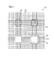
図1において、本発明の例示的な実施形態による織物構造体100の概略図が示される。本発明に従った織物構造体100は、基本構造として粗目織物(grobmaschiges Gewebe)を有し、この粗目織物は非導電性細線101で形成される。さらに、織物構造体100は、導電性細線102、107を有する。導電性細線102は、マイクロエレクトロニクス部品103を織物構造体100に組み込むためのアース(ground)として用いられる。導電性細線107は、織物構造体100に組み込むマイクロエレクトロニクス部品103の電源として用いられる。さらに、織物構造体100は、導電性細線104を有しており、この導電性細線104は、組み込むことになっているマイクロエレクトロニクス部品からのデータ伝送と、マイクロエレクトロニクス部品へのデータ伝送として用いられる。
In FIG. 1, a schematic diagram of a
導電性細線102、107および伝導性データ伝送細線104は、好ましくは、正方形のマス目構造内に設置され、その結果、正方形のマス目状の交差点105は、織物構造体100内に形成される。そのような交差点の1つの領域は、図1においてa)と記されている。
The conductive
さらに、図1においてb)と記されているそのような交差点の領域において、導電性細線102、107および伝導性データ伝送細線104が除去され、織物構造体100内のギャップを形成する。
Further, in such a region of intersection, labeled b) in FIG. 1, the
図1の領域c)においては、マイクロエレクトロニクス部品(マイクロエレクトロニクスモジュール)103が、織物構造体100内のギャップ105に配置され、導電性細線(102および107)と伝導性データ伝送細線104が、マイクロエレクトロニクスモジュール103に電力を供給し、かつ、マイクロエレクトロニクスモジュール103にデータ伝送回線を提供するために、マイクロエレクトロニクスモジュール103につながっている。本発明に従った織物構造体100において、各マイクロエレクトロニクスモジュール103は、好ましくは、導電性細線(102および107)と伝導性データ伝送細線104とのそれぞれの交差点105において配置されており、次いで、4辺からマイクロエレクトロニクスモジュール103に通じる導電性細線(102および107)と伝導性データ伝送細線104とに結合される。
In region c) of FIG. 1, a microelectronic component (microelectronic module) 103 is placed in a
マイクロエレクトロニクスモジュール103と、導電性細線(102および107)と伝導性データ伝送細線104との結合は、フレキシブルプリント回路基板と回路をつなげることによって、またはワイヤボンディングとして知られるものを用いて実現することができる。
The coupling of the
図1の領域d)において、マイクロエレクトロニクスモジュール103と、導電性細線(102および107)と伝導性データ伝送細線104との間の結合領域(接点)を絶縁させ、その上、機械的に強固で、かつ耐水性のある保護を提供するためにカプセルされたマイクロエレクトロニクスモジュール103が概略的に図示される。
In region d) of FIG. 1, the
本発明に従った織物構造体100は、いずれの場合にも、マイクロエレクトロニクスモジュール103を複数の交差点105において有する。そのような「インテリジェント」織物構造体は、壁または床の覆い、または他タイプの技術的織物の基本層または中間層として形成され得る。これは、例えば、織物コンクリート(textile concrete)構造層としても用いられ得る。織物構造体のマイクロエレクトロニクスモジュール103は、多数の異なるタイプのセンサおよび/またはアクチュエータに結合され得る。例えば、これらは、マイクロエレクトロニクスモジュールに伝送される情報を表示するためのLED、指示素子またはディスプレイであり得る。
The
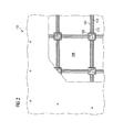
図2は、インテリジェントカーペットとして知られるものの例示的な実施形態を示す。図2の右下の角において、導電性細線102、104および107が正方形のマス目で織り込まれる粗目基本織物206が示されている。導電性細線102、104および107の交差点105において、マイクロエレクトロニクスモジュール103が粗目基本織物206内に配置される。よって、規則正しいマス目のマイクロエレクトロニクスモジュール103が製造され、マイクロエレクトロニクスモジュール103はいずれの場合においても、4辺上に供給ラインおよびデータラインとの接触を有する。加えて、マイクロエレクトロニクスモジュール103は、カプセル封入と発光ダイオードとを設けられる。さらに、図2の後部左部分において、カーペットが織物構造体100上に固定されている。
FIG. 2 shows an exemplary embodiment of what is known as an intelligent carpet. In the lower right corner of FIG. 2, a
本発明に従って、マイクロエレクトロニクス、センサおよび/またはアクチュエータ(例えば、表示ランプ)が組み込まれた織物構造体100は、本質的に十分に機能するものであり、かつ、様々なタイプの表面被覆の下に固定され得る。ここで、例を挙げると、非導電性布地、カーペットでできている床の覆い、寄木張りの床、プラスチック、カーテン、巻き上げ式ブラインド、壁の覆い、絶縁マット、テントの屋根、プラスター層、スクリードおよび織物コンクリートに言及すべきである。固定は、好ましくは、接着、積層法または加硫処理を用いて実行される。
In accordance with the present invention, a
人間の周囲で「電磁気スモッグ」を避けるために、導電性ワイヤを均一にちりばめられた布地が、本発明による織物構造体上で遮断するために用いられ得る。しかしながら、適切な場合、特定の領域、例えば容量性センサ上の領域が遮へいに覆われないように注意を払わねばならない。 In order to avoid “electromagnetic smog” around humans, fabrics evenly studded with conductive wires can be used to block on textile structures according to the present invention. However, care must be taken to ensure that certain areas, such as areas on the capacitive sensor, are not covered by shielding when appropriate.
マイクロエレクトロニクスが組み込まれた本発明による織物構造体は、好ましくは、中央制御ユニット、例えば、単純なパーソナルコンピュータに織物構造体の端部において結合される。 The fabric structure according to the invention incorporating microelectronics is preferably coupled at the end of the fabric structure to a central control unit, for example a simple personal computer.
単純なアルゴリズムを用いることによって、マイクロエレクトロニクスモジュールは、それ自身を組織化し始める。マイクロエレクトロニクスモジュールのネットワークを有する織物構造体が接続されると、すなわち、作動し始めると、次いで、学習段階が開始され、その後、各マイクロエレクトロニクスモジュールは、マス目におけるその物理的な位置が分かる。さらに、マス目を介するデータフローの経路が自動的に構成される。これは、センサまたはディスプレイ情報が織物構造体の欠陥領域の周りに導かれ得ることを意味する。ネットワークの自己組織化の結果、欠陥領域が検出され、回避される。その結果、マイクロエレクトロニクスモジュールのネットワークは、織物構造体がそれぞれの意図された使用によって定められる形に切断されても、依然として使用可能である。さらに、自己組織化は、マイクロエレクトロニクスモジュールのネットワークを手動で据え付ける労力が必要ではないという効果を有する。 By using a simple algorithm, the microelectronic module begins to organize itself. When a fabric structure with a network of microelectronic modules is connected, i.e. starts to operate, then a learning phase is started, after which each microelectronic module knows its physical position in the grid. Furthermore, a data flow path through the grid is automatically configured. This means that sensor or display information can be directed around the defective area of the fabric structure. As a result of the self-organization of the network, defective areas are detected and avoided. As a result, the network of microelectronic modules can still be used even if the fabric structure is cut into a shape defined by the respective intended use. Furthermore, self-organization has the effect that no effort is required to manually install a network of microelectronic modules.
織物構造体100のマイクロエレクトロニクス部品103間の距離を決定する方法と、自己組織化とが以下の図を用いて説明される。
A method for determining the distance between the
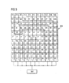
図3は、自己組織化の例が図示される本発明による織物構造体の図3において連続的に番号を付けられるマイクロエレクトロニクスモジュールの規則正しい正方形11×11ネットワークの概略図を示す。図3の規則正しい正方形11×11ネットワークは、図中で「フラッシュ」と確認される9つの欠陥マイクロエレクトロニクスモジュールを有する。描かれた線は、9つの欠陥マイクロエレクトロニクスモジュールが失敗することによって、使用できる接続経路に利用可能ではなくなった後に、この方法を用いて取得される個々のマイクロエレクトロニクスモジュールの新しい接続経路を示す。描かれた新しい接続経路は、マイクロエレクトロニクス部品間の距離を決定する方法を用いて取得している。 FIG. 3 shows a schematic diagram of an ordered square 11 × 11 network of microelectronic modules sequentially numbered in FIG. 3 of a woven structure according to the present invention in which a self-organizing example is illustrated. The regular square 11 × 11 network of FIG. 3 has nine defective microelectronic modules identified as “flash” in the figure. The drawn lines show the new connection paths of the individual microelectronic modules obtained using this method after nine defective microelectronic modules fail and become unavailable to the usable connection paths. The new connection paths drawn are obtained using a method for determining the distance between microelectronic components.
大まかに言えば、マイクロエレクトロニクス部品間の距離を決定する方法の第1の局面において、自己組織化として知られるものは、
・織物構造体内の個々のマイクロエレクトロニクス部品のローカル位置と、織物構造体の全体的な形との自己検出と、
・周期が所定の最大数内で、各マイクロエレクトロニクス部品がポータルプロセッサ302から供給される電子メッセージを取得できるように、織物構造体100において、ポータルプロセッサ302から始まって各マイクロエレクトロニクス部品103までの経路パスの自己組織化とを実行する。
Broadly speaking, in a first aspect of the method for determining the distance between microelectronic components, what is known as self-organization is
Self-detection of the local position of individual microelectronic components within the fabric structure and the overall shape of the fabric structure;
A path from the
例えば、画像データを表示すること、または音を生成することの中で、織物構造体100を実際に使用する第2の局面において、画像データ(「イメージ」)または音が、織物構造体100においてマイクロエレクトロニクス部品に結合されるアクチュエータを用いて構築される結果、データは、ポータルプロセッサ302によってマイクロエレクトロニクス部品103に送信、すなわち伝達される。反対に、マイクロエレクトロニクス部品103は、例えば、圧力センサまたは視覚センサといったセンサを用いて検出されたデータをポータルプロセッサに伝達することもできる。以下においては、一般的な適用を制限せずに、この方法がイメージデータを用いて説明される。すなわち、ディスプレイユニット(表示ユニット)が織物構造体100の個々のマイクロエレクトロニクス部品103に結合される。
For example, in a second aspect of actually using the
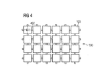
図4に示されるようにマイクロエレクトロニクス部品103が長方形、好ましくは、正方形を有する場合に、マイクロエレクトロニクス部品103は、いずれの場合においても、マイクロエレクトロニクス部品103毎に通信インターフェース401の1つを介して正方形の各辺を介して結合されるので、いずれの場合においても、織物構造体のデータ伝送細線104(以下においては、双方向接続とも呼ばれる)への、データ伝送細線104を介する4つの通信インターフェース401は、導電性細線102および107(以下においては、送電線402とも呼ばれる)を介して、その都度、それぞれのマイクロエレクトロニクス部品103に直接近接したマイクロエレクトロニクス部品103に結合される。
If the
言い換えると、これは、いずれの場合においても、2つの直接互いに近接したマイクロエレクトロニクス部品間のメッセージ交換は可能であるが、マイクロエレクトロニクス部品103の直接の近辺より大きい距離での直接のメッセージ交換は可能ではないことを意味する。
In other words, in any case, it is possible to exchange messages between two directly adjacent microelectronic components, but it is possible to exchange messages directly at a distance greater than the immediate vicinity of the
自己組織化は、文献[1]で知られる方法を用いて実行される。 Self-organization is performed using the method known from document [1].
電子メッセージを互いに近接したマイクロエレクトロニクス部品間で交換することによって、織物構造体のマイクロエレクトロニクス部品に空間を設けることを少なくとも1つの基準位置について決定する方法において、第1のメッセージは第1のマイクロエレクトロニクス部品によって生成され、第1のメッセージは、第1のマイクロエレクトロニクス部品の距離または基準位置から第1のメッセージを受信する第2のマイクロエレクトロニクス部品の距離を含む距離情報の第1の項目を含む。第1のメッセージは、第1のマイクロエレクトロニクス部品によって第2のマイクロエレクトロニクス部品に送信される。距離情報の項目によって、基準位置からの第2のマイクロエレクトロニクス部品の距離が決定または格納される。さらに、第2のメッセージは第2のマイクロエレクトロニクス部品によって生成され、第2のメッセージは、第2のマイクロエレクトロニクス部品の距離または基準位置から第2のメッセージを受信する第3のマイクロエレクトロニクス部品の距離を含む距離情報の第2の項目を含む。第2のメッセージは、第2のマイクロエレクトロニクス部品によって第3のマイクロエレクトロニクス部品に送信される。距離情報の第2の項目によって、基準位置からの第3のマイクロエレクトロニクス部品の距離が決定または格納される。前述の方法ステップは、織物構造体の全ての相互接続したマイクロエレクトロニクス部品に対して実行される。 In a method for determining for at least one reference position that a space is provided in a microelectronic component of a textile structure by exchanging electronic messages between adjacent microelectronic components, the first message comprises a first microelectronic The first message generated by the component includes a first item of distance information that includes a distance of the first microelectronic component or a distance of a second microelectronic component that receives the first message from a reference location. The first message is transmitted by the first microelectronic component to the second microelectronic component. The distance information item determines or stores the distance of the second microelectronic component from the reference position. Further, the second message is generated by the second microelectronic component, and the second message is the distance of the second microelectronic component or the distance of the third microelectronic component that receives the second message from the reference position. A second item of distance information including is included. The second message is transmitted by the second microelectronic component to the third microelectronic component. The second item of distance information determines or stores the distance of the third microelectronic component from the reference position. The foregoing method steps are performed for all interconnected microelectronic components of the textile structure.
それ故、この方法が実行された後、織物構造体内における各マイクロエレクトロニクス部品のそれぞれの位置と、少なくとも1つの基準位置に関するその距離は、ローカル情報を用いるのみで決定される。 Therefore, after this method is carried out, the respective position of each microelectronic component within the textile structure and its distance with respect to at least one reference position is determined only by using local information.
明らかに、本発明のこの局面は、マイクロシステム向けに、そしてマイクロデータディスプレイデバイスおよびセンサ向けに開発されたアーキテクチャと、その目的のために開発されたアルゴリズムとが、サービス技術および見本市技術を構築するマクロシステムに移転されており、必要なマイクロエレクトロニクス部品は、被覆素子が上に固定され得る織物構造体内に埋め込まれているという事実から分かる。 Clearly, this aspect of the present invention is that architectures developed for microsystems and for microdata display devices and sensors, and algorithms developed for that purpose, build service and trade fair technologies. It has been transferred to the macro system and the necessary microelectronic components can be seen from the fact that the covering element is embedded in a textile structure on which it can be fixed.
このようにして、多量の可能なアプリケーションが開発され、これは以下でより詳細に説明される。 In this way, a large number of possible applications are developed, which will be described in more detail below.
基準位置は、基本的に任意の所望の位置であり得る。つまり、基準位置は、好ましくは、ポータルプロセッサがある位置であり、このポータルプロセッサは以下に説明されるが、織物構造体のマイクロエレクトロニクス部品を駆動し、かつ、織物構造体の外部から通信を開始する。ポータルプロセッサは、織物構造体のマイクロエレクトロニクス部品、またはさらなるプロセッサであり得る。さらに、基準位置は、織物構造体内の位置であり得、この場合において、マイクロエレクトロニクス部品は、好ましくは基準位置に配置され、かつ、後者に割り当てられる。この場合において、基準位置は、好ましくは端部にあり、すなわち、マイクロエレクトロニクス部品が織物構造体内でマトリックスの形で行と列とに配置される場合に、一番上または一番下の行、または左側または右側の列にある。織物構造体への情報の伝送、または織物構造体からの情報の伝送は、好ましくは、織物構造体の端にあるマイクロエレクトロニクス部品のうち少なくともいくつかを排他的に介し、ポータルプロセッサを用いて実行される。 The reference position can basically be any desired position. That is, the reference position is preferably the position where the portal processor is located, which portal processor, described below, drives the microelectronic component of the fabric structure and initiates communication from outside the fabric structure. To do. The portal processor can be a microelectronic component of a woven structure or a further processor. Furthermore, the reference position may be a position within the textile structure, in which case the microelectronic component is preferably arranged at the reference position and assigned to the latter. In this case, the reference position is preferably at the end, i.e. the top or bottom row when the microelectronic components are arranged in rows and columns in the form of a matrix within the textile structure, Or in the left or right column. Transmission of information to or from the fabric structure is preferably performed using a portal processor, exclusively through at least some of the microelectronic components at the edge of the fabric structure. Is done.
明らかに、この手順は、通常、織物構造体の端における基準位置において、すなわち、織物構造体について外側のマイクロエレクトロニクス部品において、「マイクロエレクトロニクス部品を開始すること」から始めて、第1の距離は、例えば、マイクロエレクトロニクス部品がポータルプロセッサから距離「1」を有することを指定する距離値「1」を割り当てられることを意味する。それぞれのメッセージにおいて、メッセージを送信するマイクロエレクトロニクス部品の基準位置からの距離がこのメッセージ内に挿入され、マイクロエレクトロニクス部品に伝達されることによりメッセージを受信する場合に、第1のマイクロエレクトロニクス部品は、第1のメッセージにおいて第2のマイクロエレクトロニクス部品に「1」の距離値を伝達し、受信した距離値は、第2のマイクロエレクトロニクス部品によって「1」の値を増加される。増加した値「2」は、次いで、第2のマイクロエレクトロニクス部品の更新された第2の距離値として格納される。第2の距離値は値「1」を増加され、第3の距離値が生成されて、第3のマイクロエレクトロニクス部品に伝達され、そこに格納される。対応する手順が、織物構造体の全てのマイクロエレクトロニクス部品に対して対応する方法で実行され、メッセージの受信に続いて、マイクロエレクトロニクス部品にそれぞれに割り当てられた距離値は、受信した距離値が格納された距離値を下回る場合、常に距離情報の項目を更新される。 Obviously, this procedure usually starts at the reference position at the end of the fabric structure, i.e. at the outer microelectronic component with respect to the fabric structure, starting with "starting the microelectronic component", the first distance is For example, it means that a distance value “1” is assigned that specifies that the microelectronic component has a distance “1” from the portal processor. In each message, the first microelectronic component receives the message by inserting the distance from the reference location of the microelectronic component transmitting the message into this message and transmitting it to the microelectronic component: A distance value of “1” is transmitted to the second microelectronic component in the first message, and the received distance value is incremented by a value of “1” by the second microelectronic component. The increased value “2” is then stored as the updated second distance value of the second microelectronic component. The second distance value is incremented by the value “1” and a third distance value is generated and transmitted to and stored in the third microelectronic component. A corresponding procedure is performed in a corresponding manner for all microelectronic components of the woven structure, and following receipt of the message, the distance value assigned to each microelectronic component is stored with the received distance value. If the distance value is below the specified distance value, the distance information item is always updated.
織物構造体は、多数のマイクロエレクトロニクス部品を有する。各マイクロエレクトロニクス部品は、双方向通信インターフェース、データ伝送インターフェースを介して、近接した少なくとも1つのマイクロエレクトロニクス部品に結合される。織物構造体のマイクロエレクトロニクス部品のそれぞれの基準位置からの距離を決定するために、メッセージは、マイクロエレクトロニクス部品間で、好ましくは互いに近接したマイクロエレクトロニクス部品間で交換され、各メッセージは、メッセージを送信するマイクロエレクトロニクス部品またはメッセージを受信するマイクロエレクトロニクス部品の基準位置からの距離を指定する(距離値もまた指定する)距離情報の項目を含み、各マイクロエレクトロニクス部品は、基準位置について、マイクロエレクトロニクス部品の距離が受信したメッセージの距離情報から決定または格納され得るように設定される。 The woven structure has a number of microelectronic components. Each microelectronic component is coupled to at least one adjacent microelectronic component via a bi-directional communication interface, a data transmission interface. In order to determine the distance from the respective reference position of the microelectronic components of the woven structure, messages are exchanged between microelectronic components, preferably between microelectronic components in close proximity to each other, each message sending a message Includes an item of distance information (which also specifies a distance value) that specifies a distance from a reference position of the microelectronic component that receives the message or the microelectronic component that receives the message. The distance is set so that it can be determined or stored from the distance information of the received message.
ローカル情報の使用と、特に、互いに直接近接したマイクロエレクトロニクス部品間での電子メッセージの交換とのおかげで、手順は、生じる干渉と、個々のマイクロエレクトロニクス部品の不具合または例えば、織物構造体を所定の形に調整するときに2つのマイクロエレクトロニクス部品間の結合が破壊された場合に、2つのマイクロエレクトロニクス部品間の個別の結合の不具合とに関して非常に強固である。 Thanks to the use of local information and, in particular, the exchange of electronic messages between microelectronic components in close proximity to one another, the procedure determines the interference that has occurred and the failure of individual microelectronic components or, for example, a woven structure. If the connection between two microelectronic components is broken when adjusting to shape, it is very robust with respect to the failure of the individual connection between the two microelectronic components.
改良点に従って、距離を決定する方法において、マイクロエレクトロニクス部品の基準位置からの距離を決定する前に、織物構造体内でのマイクロエレクトロニクス部品のローカル位置は、織物構造体の開始点におけるマイクロエレクトロニクス部品から始まって、いずれの場合においても、少なくとも1つの行パラメータzと1つの列パラメータsとを有し、織物構造体内のメッセージを送信するマイクロエレクトロニクス部品の行番号および列番号、またはメッセージを受信するマイクロエレクトロニクス部品の行番号および列番号を含む位置を決定するメッセージが、織物構造体の近接したマイクロエレクトロニクス部品に伝達されるので決定され、かつ、以下のステップがそれぞれのマイクロエレクトロニクス部品によって実行される。受信したメッセージにおける行パラメータが、マイクロエレクトロニクス部品の前に格納された行番号より高い場合、マイクロエレクトロニクス部品の個々の行番号は、受信したメッセージの行パラメータ値zに割り当てられる。受信したメッセージにおける列番号が、マイクロエレクトロニクス部品の個々の列番号より高い場合、次いで、格納された列番号が、受信したメッセージの列パラメータ値に割り当てられる。個々の行番号および/または個々の列番号が、前述の方法ステップによって変更されている場合、次いで、新しい行パラメータと新しい列パラメータとを有する新しい位置計測メッセージが生成され、これは、いずれの場合においても、メッセージを送信するマイクロエレクトロニクス部品の行番号および列番号またはメッセージを受信するマイクロエレクトロニクス部品の行番号および列番号を含み、これらは、織物構造体の近接したマイクロエレクトロニクス部品に伝達される。 According to the refinement, in the method for determining the distance, before determining the distance from the reference position of the microelectronic component, the local position of the microelectronic component in the fabric structure is determined from the microelectronic component at the starting point of the fabric structure. Beginning in any case, the row number and column number of a microelectronic component having at least one row parameter z and one column parameter s and transmitting a message in the fabric structure, or a micro receiving message A message that determines the position including the row number and column number of the electronics part is transmitted to the adjacent microelectronic parts of the textile structure and is determined, and the following steps are performed by each microelectronic part: . If the line parameter in the received message is higher than the line number stored before the microelectronic component, the individual line number of the microelectronic component is assigned to the line parameter value z of the received message. If the column number in the received message is higher than the individual column number of the microelectronic component, then the stored column number is assigned to the column parameter value of the received message. If the individual row number and / or individual column number has been changed by the method steps described above, then a new position measurement message with a new row parameter and a new column parameter is generated, which in any case Also includes the row number and column number of the microelectronic component transmitting the message or the row number and column number of the microelectronic component receiving the message, which are communicated to the adjacent microelectronic component of the fabric structure.
この形態を用いて、互いに近接したマイクロエレクトロニクス部品間のローカルメッセージ交換に関する本発明に従った概念は、この概念に従った織物構造体内での個々のマイクロエレクトロニクス部品のローカル位置が既に、直接に近接したマイクロエレクトロニクス部品から得られた位置情報の項目にのみ由来するローカル位置情報に基づくので、さらに広がる。これにより、織物構造体の自己組織化の中で非常に耐障害性である手順が可能になる。 Using this configuration, the concept according to the invention regarding the exchange of local messages between microelectronic components in close proximity to each other is that the local position of the individual microelectronic components within the textile structure according to this concept is already in direct proximity. Since it is based on local position information derived only from the item of position information obtained from the microelectronic component, it is further expanded. This allows a very fault tolerant procedure in the self-organization of the woven structure.
本発明の他の形態に従って、反復法において、織物構造体のマイクロエレクトロニクス部品の個々の距離値は、前に格納された距離値が個々に受信したメッセージにおいて受信した距離値より大きい場合に変更され、所定の値が増加される。さらに、織物構造体のマイクロエレクトロニクス部品が個々の距離値を変更する場合に、このマイクロエレクトロニクス部品は、距離計測メッセージを生成し、それを織物構造体の近接したマイクロエレクトロニクス部品に送信し、距離計測メッセージはいずれの場合においても、距離情報の項目またはポータルプロセッサから受信するマイクロエレクトロニクス部品の距離値として個々の距離を含む。 In accordance with another aspect of the invention, in an iterative method, the individual distance values of the microelectronic components of the woven structure are changed if the previously stored distance value is greater than the distance value received in the individually received message. The predetermined value is increased. Furthermore, if the microelectronic component of the fabric structure changes individual distance values, this microelectronic component generates a distance measurement message and sends it to the adjacent microelectronic component of the fabric structure for distance measurement. In any case, the message includes the individual distance as a distance information item or a distance value of the microelectronic component received from the portal processor.
距離値は、個々の距離値について所定の値だけ増加した値、好ましくは、値「1」だけ増加され得る。 The distance value may be increased by a predetermined value for each distance value, preferably by the value “1”.
要約すると、本発明は、組み込まれたマイクロエレクトロニクスに同一のシャーシを供給する織物構造体を提供する。この織物構造体は、実質的にいかなる所望の床、天井および/または壁の覆いの下に固定され得る。よって、広い「インテリジェント範囲」が作製され得、これはセンサまたは表示面として用いられ得る。自己組織化の方法を用いて、マイクロエレクトロニクスが組み込まれた織物構造体は、マイクロエレクトロニクスモジュールが調整する間に除去されず、または効果があるマイクロエレクトロニクスモジュール間の結合ラインが除去されずに、実質的にいかなる所望の形にも切断され得る。欠陥のあるマイクロエレクトロニクスモジュールまたは欠落したマイクロエレクトロニクスモジュールは、適切な経路を用いて回避されるので、全ての機能するマイクロエレクトロニクスモジュールの機能は依然として維持され、そのような「インテリジェント範囲」を据え付けるための労力は大幅に抑えられる。 In summary, the present invention provides a woven structure that provides the same chassis for embedded microelectronics. The textile structure can be secured under virtually any desired floor, ceiling and / or wall covering. Thus, a wide “intelligent range” can be created, which can be used as a sensor or display surface. Using a method of self-organization, a textile structure incorporating microelectronics is not substantially removed while the microelectronic module is being adjusted or the effective coupling line between microelectronic modules is not removed. Can be cut into any desired shape. Defective or missing microelectronic modules are avoided using appropriate paths, so that the function of all functional microelectronic modules is still maintained and for installing such an “intelligent range” The effort is greatly reduced.
本明細書において、以下の刊行物が引用される:
[1]T.F.Sturm. S. Jung、G. Stromberg、A Stohrによる「A Novel Fault−Tolrent Architecture for Self−Organizing Display and Sensor Arrays」、International Symposium Digest of Technical Papers、volume XXXIII、No.II、Society for Information Display、Boston、Massachusetts、2002年5月22日〜23日、ページ1316〜1319、2002;
[2]独国特許出願公開第102 02 123号A1;
[3]独国特許出願公開第196 52 236号A1.
In this specification, the following publications are cited:
[1] T. F. Sturm. S. Jung, G. “A Novel Fault-Tolent Architecture for Self-Organizing Display and Sensor Arrays, International Symposium Digest Trumpet III,” by Stromberg, A Stohr. II, Society for Information Display, Boston, Massachusetts, May 22-23, 2002, pages 1316-1319, 2002;
[2] German Patent Application Publication No. 102 02 123 A1;
[3] German Patent Application Publication No. 196 52 236 A1.
101 織物構造体
101 非導電性細線
102 導電性細線(アース)
103 プロセッサユニット
104 伝導性細線(データ伝送)
105 交差点
107 導電性細線(電圧供給)
206 基本織物
302 ポータルプロセッサ
303 プロセッサユニット配置
401 双方向通信インターフェース
402 導電線
101
103
105
Claims (18)
該織物構造体に配置される複数のマイクロエレクトロニクス部品と、
該複数のマイクロエレクトロニクス部品を互いに結合する導電性細線と、
該複数のマイクロエレクトロニクス部品を互いに結合する伝導性データ伝送細線と、
非導電性細線とを、備え、
該織物構造体の端における該導電性細線および該伝導性データ伝送細線は、いずれの場合にも、電気的インターフェース、あるいはデータ伝送インターフェースを提供される、織物構造体。 A woven structure,
A plurality of microelectronic components disposed in the fabric structure;
Conductive thin wires that couple the plurality of microelectronic components together;
A conductive data transmission wire that couples the plurality of microelectronic components together;
A non-conductive thin wire,
The fabric structure, wherein the conductive wires and the conductive data transmission wires at the ends of the fabric structure are in each case provided with an electrical interface or a data transmission interface.
各メッセージは、該メッセージを送信するマイクロエレクトロニクス部品または該メッセージを受信するマイクロエレクトロニクス部品の該基準位置からの距離を指定する距離情報の項目を含み、
該複数のマイクロエレクトロニクス部品は、該基準位置からの該個々の距離は、受信したメッセージの該距離情報から決定または格納され得るように構成される、請求項1から請求項9のいずれか一項に記載の織物構造体。 The plurality of microelectronic components may be configured such that an electronic message is second adjacent to the first microelectronic component of the fabric structure to determine a respective distance from a reference position of the first microelectronic component. Configured to be exchanged with electronics components,
Each message includes an item of distance information that specifies a distance from the reference position of the microelectronic component that transmits the message or the microelectronic component that receives the message,
10. The plurality of microelectronic components are configured such that the individual distance from the reference position can be determined or stored from the distance information of a received message. The woven structure according to 1.
第1のメッセージが、第1のマイクロエレクトロニクス部品によって生成され、該第1のメッセージは、該第1のマイクロエレクトロニクス部品の距離、または該第1のメッセージを該基準位置から受信する第2のマイクロエレクトロニクス部品の距離を含む第1の距離情報を含み、
該第1のメッセージは、該第1のマイクロエレクトロニクス部品によって該第2のマイクロエレクトロニクス部品に送信され、
該距離情報によって、該基準位置からの該第2のマイクロエレクトロニクス部品の距離が決定または格納され、
第2のメッセージが、該第2のマイクロエレクトロニクス部品によって生成され、該第2のメッセージは、該第2のマイクロエレクトロニクス部品の距離、または該第2のメッセージを該基準位置から受信する第3のマイクロエレクトロニクス部品の距離を含む第2の距離情報を含み、
該第2のメッセージは、該第2のマイクロエレクトロニクス部品によって該第3のマイクロエレクトロニクス部品に送信され、
該第2の距離情報によって、該基準位置からの該第3のマイクロエレクトロニクス部品の距離が決定または格納され、
該方法ステップは、該織物構造体の該マイクロエレクトロニクス部品の全てに対して実行される、方法。 15. The microelectronic component of the textile structure according to any one of claims 1 to 10 or of the surface covering structure according to any one of claims 11 to 14 and at least one reference. A method for determining a distance between positions by exchanging electronic messages between microelectronic components in close proximity to each other, comprising:
A first message is generated by a first microelectronic component, the first message being a distance of the first microelectronic component, or a second micro that receives the first message from the reference location. Including first distance information including a distance of the electronic component;
The first message is transmitted by the first microelectronic component to the second microelectronic component;
The distance information determines or stores the distance of the second microelectronic component from the reference position;
A second message is generated by the second microelectronic component, the second message is a distance of the second microelectronic component, or a third that receives the second message from the reference location Including second distance information including the distance of the microelectronic component;
The second message is transmitted by the second microelectronic component to the third microelectronic component;
The second distance information determines or stores the distance of the third microelectronic component from the reference position;
The method wherein the method steps are performed on all of the microelectronic components of the textile structure.
該受信したメッセージにおける該行パラメータが、該マイクロエレクトロニクス部品の該前に格納された行番号より高い場合、該マイクロエレクトロニクス部品の該個々の行番号は、該受信したメッセージの該行パラメータ値zに割り当てられるステップと、
該受信したメッセージにおける該列パラメータが、該マイクロエレクトロニクス部品の該個々の列番号より高い場合、次いで、該格納された列番号が、該受信したメッセージの該列パラメータ値に割り当てられるステップと、
該個々の行番号および/または該個々の列番号が、上記の該方法ステップによって変更されている場合、次いで、新しい行パラメータと新しい列パラメータとを有する新しい位置計測メッセージが生成され、該位置計測メッセージは、いずれの場合においても、該メッセージを送信するマイクロエレクトロニクス部品の行番号および列番号、または該メッセージを受信するマイクロエレクトロニクス部品の行番号および列番号を含み、これらは、該織物構造体の近接したマイクロエレクトロニクス部品によって実行される、請求項15に記載の方法。 Prior to determining the distance of the microelectronic component from the reference position, the local position of the microelectronic component within the fabric structure is any starting from the microelectronic component at the starting point of the fabric structure. In some cases, the row number and column number of a microelectronic component that has at least one row parameter z and one column parameter s and sends a message in the fabric structure, or the row of a microelectronic component that receives the message. A message determining a position including a number and a column number is determined by being communicated to adjacent microelectronic components of the textile structure;
If the row parameter in the received message is higher than the previously stored row number of the microelectronic component, the individual row number of the microelectronic component is set to the row parameter value z of the received message. Assigned steps,
If the column parameter in the received message is higher than the individual column number of the microelectronic component, then the stored column number is assigned to the column parameter value of the received message;
If the individual row number and / or the individual column number has been changed by the method steps described above, then a new position measurement message with a new row parameter and a new column parameter is generated and the position measurement The message in each case includes the row number and column number of the microelectronic component sending the message or the row number and column number of the microelectronic component receiving the message, which are The method of claim 15, wherein the method is performed by adjacent microelectronic components.
該織物構造体のマイクロエレクトロニクス部品が該個々の距離値を変更する場合に、このマイクロエレクトロニクス部品は、距離計測メッセージを生成し、それを該織物構造体の近接したマイクロエレクトロニクス部品に送信し、該距離計測メッセージは、いずれの場合においても、距離情報としての個々の距離か、あるいはポータルプロセッサから受信するマイクロエレクトロニクス部品が有する距離値を含む、請求項15または請求項16に記載の方法。 In an iterative method, the individual distance values of the microelectronic components of the textile structure are changed if the previously stored distance value is greater than the distance value received in the respective received message, and only a predetermined value. Increased,
When the microelectronic component of the textile structure changes the individual distance values, the microelectronic component generates a distance measurement message and sends it to the adjacent microelectronic component of the textile structure, The method according to claim 15 or 16, wherein the distance measurement message includes in each case an individual distance as distance information or a distance value possessed by the microelectronic component received from the portal processor.
Applications Claiming Priority (2)
| Application Number | Priority Date | Filing Date | Title |
|---|---|---|---|
| DE2003107505 DE10307505B4 (en) | 2003-02-21 | 2003-02-21 | A textile fabric structure, surface covering structure and method for determining a spacing of microelectronic elements of the textile fabric structure to at least one reference position |
| PCT/DE2004/000314 WO2004076731A1 (en) | 2003-02-21 | 2004-02-19 | Textile fabric structure, surface covering structure and method for determining the interspacing of microelectronic elements of the textile fabric structure with respect to at least one reference position |
Publications (1)
| Publication Number | Publication Date |
|---|---|
| JP2006517618A true JP2006517618A (en) | 2006-07-27 |
Family
ID=32841783
Family Applications (1)
| Application Number | Title | Priority Date | Filing Date |
|---|---|---|---|
| JP2005518397A Pending JP2006517618A (en) | 2003-02-21 | 2004-02-19 | Woven structure, surface covering structure, and method for determining a distance of a microelectronic element of a woven structure relative to at least one reference position |
Country Status (6)
| Country | Link |
|---|---|
| US (1) | US20060035554A1 (en) |
| EP (1) | EP1595013A1 (en) |
| JP (1) | JP2006517618A (en) |
| CN (1) | CN1751148A (en) |
| DE (1) | DE10307505B4 (en) |
| WO (1) | WO2004076731A1 (en) |
Cited By (5)
| Publication number | Priority date | Publication date | Assignee | Title |
|---|---|---|---|---|
| JP2006299457A (en) * | 2005-04-20 | 2006-11-02 | Hideo Hirose | Light-emitting cloth or light-emitting band |
| JP2012503324A (en) * | 2008-09-19 | 2012-02-02 | コーニンクレッカ フィリップス エレクトロニクス エヌ ヴィ | Electronic textile and method for determining functional area of electronic textile |
| JP2013519225A (en) * | 2010-02-03 | 2013-05-23 | コミサリア ア レネルジー アトミック エ オ ゼネルジー アルテルナティブ | Method for incorporating at least one tip using a fabric and fabric comprising a tip device |
| JP2018538765A (en) * | 2016-02-04 | 2018-12-27 | ゾン シンシァォZENG Xinxiao | Voice communication method, system, and medium |
| KR20200033162A (en) * | 2018-09-19 | 2020-03-27 | 애플 인크. | Fabric items with electrical components |
Families Citing this family (77)
| Publication number | Priority date | Publication date | Assignee | Title |
|---|---|---|---|---|
| US7825346B2 (en) * | 2004-08-27 | 2010-11-02 | Jack Chu | Low powered activation electronic device |
| EP1727408A1 (en) * | 2005-05-13 | 2006-11-29 | Eidgenössische Technische Hochschule Zürich | Textile with conductor pattern and method for its production |
| ATE381250T1 (en) * | 2005-05-13 | 2007-12-15 | Sefar Ag | CIRCUIT BOARD AND METHOD FOR THE PRODUCTION THEREOF |
| DE102005033643A1 (en) * | 2005-07-19 | 2007-02-01 | Sennheiser Electronic Gmbh & Co. Kg | Textile material for an article of clothing comprises electrical and/or electronic components and/or lines embedded in the material |
| DE102005038798A1 (en) * | 2005-08-17 | 2007-03-01 | Future-Shape Gmbh | Robot e.g. transport robot, position determination system for use in e.g. hospital, has computing unit to convert coordinates of network into map plotting information, and read unit to read data and receive information from computing unit |
| DE102005052005B4 (en) | 2005-10-31 | 2007-10-18 | Infineon Technologies Ag | Processor arrangement |
| CN101384186B (en) * | 2006-02-15 | 2012-07-18 | 皇家飞利浦电子股份有限公司 | A structure of fabric and electronic components |
| DE102006017540A1 (en) * | 2006-04-13 | 2007-10-18 | Drägerwerk AG | Textile system with a variety of electronic functional elements |
| US20100026614A1 (en) * | 2006-05-24 | 2010-02-04 | Koninklijke Philips Electronics, N.V. | Method and apparatus for auto-commissioning of led based display configurations |
| DE102006027213A1 (en) * | 2006-06-12 | 2007-12-13 | Future-Shape Gmbh | Textile layer arrangement, textile layer array and method for producing a textile layer arrangement |
| DE102006039787A1 (en) * | 2006-08-24 | 2008-03-20 | Siemens Ag | Method for detection of object as passive goal of marking by light beam, involves mounting organic photo diode on object and organic photo diode is in stack structure form provided with top electrode, bottom electrode and carrier substrate |
| DE102007001225A1 (en) * | 2007-01-08 | 2008-07-10 | Future-Shape Gmbh | Surface covering element, surface covering element arrangement and method for producing a surface covering element |
| KR20090127179A (en) * | 2007-03-29 | 2009-12-09 | 코닌클리케 필립스 일렉트로닉스 엔.브이. | Survey-based display device and control method thereof |
| DE102008010530A1 (en) * | 2008-02-22 | 2009-08-27 | Future-Shape Gmbh | A method of making a flooring pad and method of making a flooring layer for a flooring pad having at least one electronic component integrated therein |
| CN102912521B (en) * | 2008-05-28 | 2015-04-01 | 瑟尔瑞株式会社 | Electrically conductive pad and a production method thereof |
| US9758907B2 (en) * | 2008-09-22 | 2017-09-12 | Intel Corporation | Method and apparatus for attaching chip to a textile |
| CH700060A1 (en) * | 2008-12-04 | 2010-06-15 | Forster Rohner Ag | Method for attaching flat electronic components, such as solar cells, on a flexible sheet. |
| DE102009031568A1 (en) * | 2009-06-29 | 2010-12-30 | Fraunhofer-Gesellschaft zur Förderung der angewandten Forschung e.V. | Method for producing an electronic system, method for producing a free-form surface with such a system, as well as electronic system and free-form surfaces with such a system |
| KR20120081607A (en) * | 2009-09-24 | 2012-07-19 | 코닌클리즈케 필립스 일렉트로닉스 엔.브이. | Electronic textile with local energy supply devices |
| FR2962593B1 (en) | 2010-07-06 | 2014-03-28 | Commissariat Energie Atomique | METHOD FOR ASSEMBLING A CHIP IN A FLEXIBLE SUBSTRATE |
| CN103109586B (en) * | 2010-09-21 | 2017-02-15 | 皇家飞利浦电子股份有限公司 | Electronic textile and method of manufacturing an electronic textile |
| RU2013118210A (en) * | 2010-09-22 | 2014-10-27 | Конинклейке Филипс Электроникс Н.В. | JACKET FROM KNITTED TEXTILE WITH VARIOUS BINDING SCHEMES AND ELECTRONIC FABRIC |
| EP2522794A1 (en) | 2011-05-13 | 2012-11-14 | Carpet Concept Objekt-Teppichboden GmbH | System for energy and/or data production and contacting unit for same |
| DE102011088004A1 (en) * | 2011-12-08 | 2013-06-13 | Siemens Aktiengesellschaft | System for detection of object e.g. baggage, in security check in airport, has data interfaces provided at edges adjacent to touch-sensitive surface covering elements for transmission of sensory detected contact data |
| US8948839B1 (en) | 2013-08-06 | 2015-02-03 | L.I.F.E. Corporation S.A. | Compression garments having stretchable and conductive ink |
| US8945328B2 (en) | 2012-09-11 | 2015-02-03 | L.I.F.E. Corporation S.A. | Methods of making garments having stretchable and conductive ink |
| US11246213B2 (en) | 2012-09-11 | 2022-02-08 | L.I.F.E. Corporation S.A. | Physiological monitoring garments |
| US9817440B2 (en) | 2012-09-11 | 2017-11-14 | L.I.F.E. Corporation S.A. | Garments having stretchable and conductive ink |
| US10201310B2 (en) | 2012-09-11 | 2019-02-12 | L.I.F.E. Corporation S.A. | Calibration packaging apparatuses for physiological monitoring garments |
| US10159440B2 (en) | 2014-03-10 | 2018-12-25 | L.I.F.E. Corporation S.A. | Physiological monitoring garments |
| US10462898B2 (en) | 2012-09-11 | 2019-10-29 | L.I.F.E. Corporation S.A. | Physiological monitoring garments |
| SMT201800692T1 (en) | 2012-09-11 | 2019-01-11 | Life Corp Sa | WEARABLE COMMUNICATION PLATFORM |
| US10081887B2 (en) * | 2012-12-14 | 2018-09-25 | Intel Corporation | Electrically functional fabric for flexible electronics |
| US10231333B1 (en) | 2013-08-27 | 2019-03-12 | Flextronics Ap, Llc. | Copper interconnect for PTH components assembly |
| US9554465B1 (en) | 2013-08-27 | 2017-01-24 | Flextronics Ap, Llc | Stretchable conductor design and methods of making |
| US9674949B1 (en) | 2013-08-27 | 2017-06-06 | Flextronics Ap, Llc | Method of making stretchable interconnect using magnet wires |
| US9521748B1 (en) | 2013-12-09 | 2016-12-13 | Multek Technologies, Ltd. | Mechanical measures to limit stress and strain in deformable electronics |
| US9338915B1 (en) | 2013-12-09 | 2016-05-10 | Flextronics Ap, Llc | Method of attaching electronic module on fabrics by stitching plated through holes |
| WO2015103620A1 (en) | 2014-01-06 | 2015-07-09 | Andrea Aliverti | Systems and methods to automatically determine garment fit |
| US9766171B2 (en) | 2014-03-17 | 2017-09-19 | Columbia Insurance Company | Devices, systems and method for flooring performance testing |
| US9575560B2 (en) | 2014-06-03 | 2017-02-21 | Google Inc. | Radar-based gesture-recognition through a wearable device |
| US9811164B2 (en) | 2014-08-07 | 2017-11-07 | Google Inc. | Radar-based gesture sensing and data transmission |
| US9921660B2 (en) | 2014-08-07 | 2018-03-20 | Google Llc | Radar-based gesture recognition |
| US9588625B2 (en) | 2014-08-15 | 2017-03-07 | Google Inc. | Interactive textiles |
| US10268321B2 (en) | 2014-08-15 | 2019-04-23 | Google Llc | Interactive textiles within hard objects |
| US9778749B2 (en) | 2014-08-22 | 2017-10-03 | Google Inc. | Occluded gesture recognition |
| US11169988B2 (en) | 2014-08-22 | 2021-11-09 | Google Llc | Radar recognition-aided search |
| US9839123B2 (en) * | 2014-09-29 | 2017-12-05 | Imec Vzw | Smart textile product and method for fabricating the same |
| KR102235414B1 (en) * | 2014-09-30 | 2021-04-01 | 애플 인크. | Fabric with embedded electrical components |
| US9600080B2 (en) | 2014-10-02 | 2017-03-21 | Google Inc. | Non-line-of-sight radar-based gesture recognition |
| US9516422B2 (en) * | 2015-02-16 | 2016-12-06 | Hiroshi Ohara | Weaving method for a damper of a loudspeaker |
| US10016162B1 (en) | 2015-03-23 | 2018-07-10 | Google Llc | In-ear health monitoring |
| US9983747B2 (en) | 2015-03-26 | 2018-05-29 | Google Llc | Two-layer interactive textiles |
| EP3885882A1 (en) | 2015-04-30 | 2021-09-29 | Google LLC | Rf-based micro-motion tracking for gesture tracking and recognition |
| CN107430443B (en) | 2015-04-30 | 2020-07-10 | 谷歌有限责任公司 | Gesture recognition based on wide field radar |
| JP6517356B2 (en) | 2015-04-30 | 2019-05-22 | グーグル エルエルシー | Type-independent RF signal representation |
| US10088908B1 (en) | 2015-05-27 | 2018-10-02 | Google Llc | Gesture detection and interactions |
| US9693592B2 (en) * | 2015-05-27 | 2017-07-04 | Google Inc. | Attaching electronic components to interactive textiles |
| KR102593337B1 (en) | 2015-07-20 | 2023-10-23 | 엘.아이.에프.이. 코포레이션 에스.에이. | Flexible fabric ribbon connectors for clothing with sensors and electronics |
| DE102015112214A1 (en) * | 2015-07-27 | 2017-02-02 | <BARIT>(R) - Kunstharz-BELAGSTECHNIK GmbH | Floor covering with at least one electrical component and method for producing a floor covering |
| US10817065B1 (en) | 2015-10-06 | 2020-10-27 | Google Llc | Gesture recognition using multiple antenna |
| EP3371855A1 (en) | 2015-11-04 | 2018-09-12 | Google LLC | Connectors for connecting electronics embedded in garments to external devices |
| WO2017192167A1 (en) | 2016-05-03 | 2017-11-09 | Google Llc | Connecting an electronic component to an interactive textile |
| US10175781B2 (en) | 2016-05-16 | 2019-01-08 | Google Llc | Interactive object with multiple electronics modules |
| KR20190025965A (en) | 2016-07-01 | 2019-03-12 | 엘.아이.에프.이. 코포레이션 에스.에이. | Identification of biometrics by garments having multiple sensors |
| DE102016114319B4 (en) * | 2016-08-03 | 2019-02-28 | Inteca Gmbh | Flat lighting device |
| CN106529003A (en) * | 2016-11-04 | 2017-03-22 | 浙江华尔纺织科技有限公司 | Wiring structure, clothes and wiring method |
| CN106263096B (en) * | 2016-11-04 | 2018-04-03 | 浙江华尔纺织科技有限公司 | Conductor structure and intelligent clothing |
| CN106388025B (en) * | 2016-11-04 | 2020-07-28 | 华尔科技集团股份有限公司 | Wiring structure, clothes and wiring method |
| CN106490702B (en) * | 2016-11-04 | 2018-09-28 | 华尔科技集团股份有限公司 | Wire structures, clothing and wiring method |
| US10579150B2 (en) | 2016-12-05 | 2020-03-03 | Google Llc | Concurrent detection of absolute distance and relative movement for sensing action gestures |
| DE102017119425A1 (en) * | 2017-02-01 | 2018-08-02 | <BARIT>(R) - Kunstharz-BELAGSTECHNIK GmbH | Floor covering with at least one electrical component and electrical component for a floor covering |
| US11401632B2 (en) | 2018-02-06 | 2022-08-02 | Microsoft Technology Licensing, Llc | Electronic functionality in textiles |
| US10687421B1 (en) * | 2018-04-04 | 2020-06-16 | Flex Ltd. | Fabric with woven wire braid |
| CN109234887A (en) * | 2018-12-03 | 2019-01-18 | 张坤 | A kind of sensing fabric and its batch method for weaving that output signal strength is high |
| CN114753040B (en) * | 2022-03-10 | 2024-04-26 | 珠海泓利织带有限公司 | Ribbon with data acquisition and transmission functions and method thereof |
| WO2025208213A1 (en) * | 2024-04-01 | 2025-10-09 | Myant Corp. | Conductive yarns with insulated coating and methods of assembling textiles including same |
Citations (4)
| Publication number | Priority date | Publication date | Assignee | Title |
|---|---|---|---|---|
| JPH11168268A (en) * | 1997-09-24 | 1999-06-22 | Massachusetts Inst Of Technol <Mit> | Electrically active fabrics and objects created therefrom |
| JP2002517301A (en) * | 1998-05-13 | 2002-06-18 | ジョージア テック リサーチ コーポレイション | Fabric or garment with integrated flexible information infrastructure |
| WO2002084617A1 (en) * | 2001-04-10 | 2002-10-24 | Philip Noel Leonard | Electronic systems incorporated into textile threads or fibres |
| JP2005524783A (en) * | 2002-05-10 | 2005-08-18 | サーノフ・コーポレーション | Electronic woven fabric, yarn and fabric |
Family Cites Families (8)
| Publication number | Priority date | Publication date | Assignee | Title |
|---|---|---|---|---|
| BE530615A (en) * | 1953-07-28 | |||
| US3631298A (en) * | 1969-10-24 | 1971-12-28 | Bunker Ramo | Woven interconnection structure |
| DE19652236A1 (en) * | 1996-12-16 | 1998-06-18 | Raetz Walter | Electromagnetic monitoring of integrity of conveyor belt |
| US6080690A (en) * | 1998-04-29 | 2000-06-27 | Motorola, Inc. | Textile fabric with integrated sensing device and clothing fabricated thereof |
| CN1390109A (en) * | 1999-07-06 | 2003-01-08 | 佐治亚科技研究公司 | Fabric or garment for monitoring vital signs of infants |
| FR2818476B1 (en) * | 2000-12-20 | 2004-06-11 | France Telecom | PORTABLE ELECTRONIC EQUIPMENT |
| US6852395B2 (en) * | 2002-01-08 | 2005-02-08 | North Carolina State University | Methods and systems for selectively connecting and disconnecting conductors in a fabric |
| DE10202123A1 (en) * | 2002-01-21 | 2003-07-31 | Infineon Technologies Ag | Method and device for integrating electronics in textiles |
-
2003
- 2003-02-21 DE DE2003107505 patent/DE10307505B4/en not_active Expired - Fee Related
-
2004
- 2004-02-19 CN CNA2004800046758A patent/CN1751148A/en active Pending
- 2004-02-19 WO PCT/DE2004/000314 patent/WO2004076731A1/en not_active Ceased
- 2004-02-19 EP EP04712472A patent/EP1595013A1/en not_active Withdrawn
- 2004-02-19 JP JP2005518397A patent/JP2006517618A/en active Pending
-
2005
- 2005-08-19 US US11/207,599 patent/US20060035554A1/en not_active Abandoned
Patent Citations (4)
| Publication number | Priority date | Publication date | Assignee | Title |
|---|---|---|---|---|
| JPH11168268A (en) * | 1997-09-24 | 1999-06-22 | Massachusetts Inst Of Technol <Mit> | Electrically active fabrics and objects created therefrom |
| JP2002517301A (en) * | 1998-05-13 | 2002-06-18 | ジョージア テック リサーチ コーポレイション | Fabric or garment with integrated flexible information infrastructure |
| WO2002084617A1 (en) * | 2001-04-10 | 2002-10-24 | Philip Noel Leonard | Electronic systems incorporated into textile threads or fibres |
| JP2005524783A (en) * | 2002-05-10 | 2005-08-18 | サーノフ・コーポレーション | Electronic woven fabric, yarn and fabric |
Cited By (7)
| Publication number | Priority date | Publication date | Assignee | Title |
|---|---|---|---|---|
| JP2006299457A (en) * | 2005-04-20 | 2006-11-02 | Hideo Hirose | Light-emitting cloth or light-emitting band |
| JP2012503324A (en) * | 2008-09-19 | 2012-02-02 | コーニンクレッカ フィリップス エレクトロニクス エヌ ヴィ | Electronic textile and method for determining functional area of electronic textile |
| JP2013519225A (en) * | 2010-02-03 | 2013-05-23 | コミサリア ア レネルジー アトミック エ オ ゼネルジー アルテルナティブ | Method for incorporating at least one tip using a fabric and fabric comprising a tip device |
| JP2018538765A (en) * | 2016-02-04 | 2018-12-27 | ゾン シンシァォZENG Xinxiao | Voice communication method, system, and medium |
| KR20200033162A (en) * | 2018-09-19 | 2020-03-27 | 애플 인크. | Fabric items with electrical components |
| KR102204792B1 (en) * | 2018-09-19 | 2021-01-18 | 애플 인크. | Fabric items with electrical components |
| US11668026B2 (en) | 2018-09-19 | 2023-06-06 | Apple Inc. | Fabric items with electrical components |
Also Published As
| Publication number | Publication date |
|---|---|
| WO2004076731A1 (en) | 2004-09-10 |
| CN1751148A (en) | 2006-03-22 |
| DE10307505A1 (en) | 2004-09-09 |
| DE10307505B4 (en) | 2005-03-03 |
| US20060035554A1 (en) | 2006-02-16 |
| EP1595013A1 (en) | 2005-11-16 |
Similar Documents
| Publication | Publication Date | Title |
|---|---|---|
| JP2006517618A (en) | Woven structure, surface covering structure, and method for determining a distance of a microelectronic element of a woven structure relative to at least one reference position | |
| US7941676B2 (en) | Processor array having a multiplicity of processor elements and method of transmitting electricity between processor elements | |
| JP2006514381A (en) | SURFACE PANEL MODULE, SURFACE PANEL MODULE STRUCTURE, METHOD FOR DETERMINING A DISTANCE FROM A SURFACE PANEL MODULE OF A SURFACE PANEL MODULE TO AT LEAST ONE REFERENCE POSITION | |
| JP5841132B2 (en) | Transmitter module used in modular power transmission system | |
| US20070018083A1 (en) | Structural health monitoring layer having distributed electronics | |
| WO2000075417A1 (en) | Floor covering with sensor | |
| JP2011053212A (en) | Sensor system for periphery monitoring using mechanical component, and method of drive-controlling and evaluating the same | |
| DK2766885T3 (en) | PLANAR SENSOR AND ITS PREPARATION PROCEDURE | |
| Lauterbach et al. | A large-area sensor system underneath the floor for ambient assisted living applications | |
| JP2008541003A (en) | Underfloor heating element | |
| KR102525922B1 (en) | Apparatus for detecting rain using wire mesh sensor | |
| CN104246687A (en) | panel with electrical equipment | |
| JP3585266B2 (en) | Construction method of heating equipment using planar heating element | |
| CN111989722A (en) | Sensor pad for area sensor system, area sensor system, and sensor pad manufacturing method | |
| US20250216229A1 (en) | Electronic Device | |
| Lauterbach et al. | A self-organizing and fault-tolerant wired peer-to-peer sensor network for textile applications | |
| DE102005035383B4 (en) | Processor element, method for initializing a processor arrangement and processor arrangement | |
| JP4185867B2 (en) | Floor heating system | |
| JP2002267196A (en) | Heating and non-heating mats and floorboards for floor heating floors | |
| JPH11281076A (en) | Heating unit for floor heating and floor heating structure using the heating unit for floor heating | |
| CN102333994A (en) | Planar electrode system | |
| JP4193762B2 (en) | Planar heating element and floor heating device using the same | |
| JPH0659713U (en) | Floor heating system | |
| JP2005061163A (en) | Floor heating system | |
| JP2002243179A (en) | Floor heating floor construction method and floor heating floor structure |
Legal Events
| Date | Code | Title | Description |
|---|---|---|---|
| A977 | Report on retrieval |
Free format text: JAPANESE INTERMEDIATE CODE: A971007 Effective date: 20080417 |
|
| A131 | Notification of reasons for refusal |
Free format text: JAPANESE INTERMEDIATE CODE: A131 Effective date: 20080421 |
|
| A601 | Written request for extension of time |
Free format text: JAPANESE INTERMEDIATE CODE: A601 Effective date: 20080716 |
|
| A602 | Written permission of extension of time |
Free format text: JAPANESE INTERMEDIATE CODE: A602 Effective date: 20080724 |
|
| A02 | Decision of refusal |
Free format text: JAPANESE INTERMEDIATE CODE: A02 Effective date: 20081014 |